EP2148376A2 - Procédé et dispositif destinés à la commutation de cellules solaires dans un module photovoltaïque - Google Patents
Procédé et dispositif destinés à la commutation de cellules solaires dans un module photovoltaïque Download PDFInfo
- Publication number
- EP2148376A2 EP2148376A2 EP20090009354 EP09009354A EP2148376A2 EP 2148376 A2 EP2148376 A2 EP 2148376A2 EP 20090009354 EP20090009354 EP 20090009354 EP 09009354 A EP09009354 A EP 09009354A EP 2148376 A2 EP2148376 A2 EP 2148376A2
- Authority
- EP
- European Patent Office
- Prior art keywords
- contact strip
- heating
- contact
- solar cells
- conductive adhesive
- Prior art date
- Legal status (The legal status is an assumption and is not a legal conclusion. Google has not performed a legal analysis and makes no representation as to the accuracy of the status listed.)
- Withdrawn
Links
- 238000000034 method Methods 0.000 title claims abstract description 33
- 238000010438 heat treatment Methods 0.000 claims abstract description 74
- 230000001070 adhesive effect Effects 0.000 claims abstract description 46
- 239000000853 adhesive Substances 0.000 claims abstract description 45
- 229920003023 plastic Polymers 0.000 claims abstract description 8
- 239000004033 plastic Substances 0.000 claims abstract description 5
- 239000000463 material Substances 0.000 claims description 3
- 230000003213 activating effect Effects 0.000 claims 1
- 230000001276 controlling effect Effects 0.000 claims 1
- 238000012544 monitoring process Methods 0.000 claims 1
- 230000001105 regulatory effect Effects 0.000 claims 1
- 230000004913 activation Effects 0.000 abstract description 5
- 239000011521 glass Substances 0.000 description 14
- 238000003475 lamination Methods 0.000 description 5
- 238000004519 manufacturing process Methods 0.000 description 5
- 238000004132 cross linking Methods 0.000 description 4
- 239000010409 thin film Substances 0.000 description 4
- 239000012790 adhesive layer Substances 0.000 description 3
- 238000011109 contamination Methods 0.000 description 3
- 239000007789 gas Substances 0.000 description 3
- 239000010410 layer Substances 0.000 description 3
- 238000012545 processing Methods 0.000 description 3
- 229910000639 Spring steel Inorganic materials 0.000 description 2
- 239000002390 adhesive tape Substances 0.000 description 2
- 239000002131 composite material Substances 0.000 description 2
- 238000010292 electrical insulation Methods 0.000 description 2
- 238000001465 metallisation Methods 0.000 description 2
- 230000008646 thermal stress Effects 0.000 description 2
- RYGMFSIKBFXOCR-UHFFFAOYSA-N Copper Chemical compound [Cu] RYGMFSIKBFXOCR-UHFFFAOYSA-N 0.000 description 1
- 239000004696 Poly ether ether ketone Substances 0.000 description 1
- JUPQTSLXMOCDHR-UHFFFAOYSA-N benzene-1,4-diol;bis(4-fluorophenyl)methanone Chemical compound OC1=CC=C(O)C=C1.C1=CC(F)=CC=C1C(=O)C1=CC=C(F)C=C1 JUPQTSLXMOCDHR-UHFFFAOYSA-N 0.000 description 1
- 230000015572 biosynthetic process Effects 0.000 description 1
- DQXBYHZEEUGOBF-UHFFFAOYSA-N but-3-enoic acid;ethene Chemical compound C=C.OC(=O)CC=C DQXBYHZEEUGOBF-UHFFFAOYSA-N 0.000 description 1
- 238000004140 cleaning Methods 0.000 description 1
- 238000001816 cooling Methods 0.000 description 1
- 229910052802 copper Inorganic materials 0.000 description 1
- 239000010949 copper Substances 0.000 description 1
- 230000006735 deficit Effects 0.000 description 1
- 238000013461 design Methods 0.000 description 1
- 238000011161 development Methods 0.000 description 1
- 230000018109 developmental process Effects 0.000 description 1
- 238000010586 diagram Methods 0.000 description 1
- 230000000694 effects Effects 0.000 description 1
- 238000005265 energy consumption Methods 0.000 description 1
- 239000005038 ethylene vinyl acetate Substances 0.000 description 1
- 230000005284 excitation Effects 0.000 description 1
- 238000002474 experimental method Methods 0.000 description 1
- 239000012530 fluid Substances 0.000 description 1
- 239000003779 heat-resistant material Substances 0.000 description 1
- 239000012535 impurity Substances 0.000 description 1
- 230000002045 lasting effect Effects 0.000 description 1
- 238000001208 nuclear magnetic resonance pulse sequence Methods 0.000 description 1
- 235000011837 pasties Nutrition 0.000 description 1
- 229920001200 poly(ethylene-vinyl acetate) Polymers 0.000 description 1
- 229920002530 polyetherether ketone Polymers 0.000 description 1
- 229920000642 polymer Polymers 0.000 description 1
- 239000004810 polytetrafluoroethylene Substances 0.000 description 1
- 229920001343 polytetrafluoroethylene Polymers 0.000 description 1
- 230000000284 resting effect Effects 0.000 description 1
- 239000004065 semiconductor Substances 0.000 description 1
- 230000035939 shock Effects 0.000 description 1
- 230000035882 stress Effects 0.000 description 1
- 239000000758 substrate Substances 0.000 description 1
Images

Classifications
-
- H—ELECTRICITY
- H01—ELECTRIC ELEMENTS
- H01L—SEMICONDUCTOR DEVICES NOT COVERED BY CLASS H10
- H01L31/00—Semiconductor devices sensitive to infrared radiation, light, electromagnetic radiation of shorter wavelength or corpuscular radiation and specially adapted either for the conversion of the energy of such radiation into electrical energy or for the control of electrical energy by such radiation; Processes or apparatus specially adapted for the manufacture or treatment thereof or of parts thereof; Details thereof
- H01L31/04—Semiconductor devices sensitive to infrared radiation, light, electromagnetic radiation of shorter wavelength or corpuscular radiation and specially adapted either for the conversion of the energy of such radiation into electrical energy or for the control of electrical energy by such radiation; Processes or apparatus specially adapted for the manufacture or treatment thereof or of parts thereof; Details thereof adapted as photovoltaic [PV] conversion devices
- H01L31/042—PV modules or arrays of single PV cells
- H01L31/05—Electrical interconnection means between PV cells inside the PV module, e.g. series connection of PV cells
-
- H—ELECTRICITY
- H01—ELECTRIC ELEMENTS
- H01L—SEMICONDUCTOR DEVICES NOT COVERED BY CLASS H10
- H01L24/00—Arrangements for connecting or disconnecting semiconductor or solid-state bodies; Methods or apparatus related thereto
- H01L24/01—Means for bonding being attached to, or being formed on, the surface to be connected, e.g. chip-to-package, die-attach, "first-level" interconnects; Manufacturing methods related thereto
- H01L24/26—Layer connectors, e.g. plate connectors, solder or adhesive layers; Manufacturing methods related thereto
- H01L24/28—Structure, shape, material or disposition of the layer connectors prior to the connecting process
-
- H—ELECTRICITY
- H01—ELECTRIC ELEMENTS
- H01L—SEMICONDUCTOR DEVICES NOT COVERED BY CLASS H10
- H01L31/00—Semiconductor devices sensitive to infrared radiation, light, electromagnetic radiation of shorter wavelength or corpuscular radiation and specially adapted either for the conversion of the energy of such radiation into electrical energy or for the control of electrical energy by such radiation; Processes or apparatus specially adapted for the manufacture or treatment thereof or of parts thereof; Details thereof
- H01L31/18—Processes or apparatus specially adapted for the manufacture or treatment of these devices or of parts thereof
- H01L31/1876—Particular processes or apparatus for batch treatment of the devices
- H01L31/188—Apparatus specially adapted for automatic interconnection of solar cells in a module
-
- H—ELECTRICITY
- H01—ELECTRIC ELEMENTS
- H01L—SEMICONDUCTOR DEVICES NOT COVERED BY CLASS H10
- H01L2924/00—Indexing scheme for arrangements or methods for connecting or disconnecting semiconductor or solid-state bodies as covered by H01L24/00
- H01L2924/01—Chemical elements
- H01L2924/01005—Boron [B]
-
- H—ELECTRICITY
- H01—ELECTRIC ELEMENTS
- H01L—SEMICONDUCTOR DEVICES NOT COVERED BY CLASS H10
- H01L2924/00—Indexing scheme for arrangements or methods for connecting or disconnecting semiconductor or solid-state bodies as covered by H01L24/00
- H01L2924/01—Chemical elements
- H01L2924/0102—Calcium [Ca]
-
- H—ELECTRICITY
- H01—ELECTRIC ELEMENTS
- H01L—SEMICONDUCTOR DEVICES NOT COVERED BY CLASS H10
- H01L2924/00—Indexing scheme for arrangements or methods for connecting or disconnecting semiconductor or solid-state bodies as covered by H01L24/00
- H01L2924/01—Chemical elements
- H01L2924/01029—Copper [Cu]
-
- H—ELECTRICITY
- H01—ELECTRIC ELEMENTS
- H01L—SEMICONDUCTOR DEVICES NOT COVERED BY CLASS H10
- H01L2924/00—Indexing scheme for arrangements or methods for connecting or disconnecting semiconductor or solid-state bodies as covered by H01L24/00
- H01L2924/01—Chemical elements
- H01L2924/01068—Erbium [Er]
-
- H—ELECTRICITY
- H01—ELECTRIC ELEMENTS
- H01L—SEMICONDUCTOR DEVICES NOT COVERED BY CLASS H10
- H01L2924/00—Indexing scheme for arrangements or methods for connecting or disconnecting semiconductor or solid-state bodies as covered by H01L24/00
- H01L2924/01—Chemical elements
- H01L2924/01082—Lead [Pb]
-
- H—ELECTRICITY
- H01—ELECTRIC ELEMENTS
- H01L—SEMICONDUCTOR DEVICES NOT COVERED BY CLASS H10
- H01L2924/00—Indexing scheme for arrangements or methods for connecting or disconnecting semiconductor or solid-state bodies as covered by H01L24/00
- H01L2924/06—Polymers
- H01L2924/078—Adhesive characteristics other than chemical
- H01L2924/0781—Adhesive characteristics other than chemical being an ohmic electrical conductor
- H01L2924/07811—Extrinsic, i.e. with electrical conductive fillers
-
- H—ELECTRICITY
- H01—ELECTRIC ELEMENTS
- H01L—SEMICONDUCTOR DEVICES NOT COVERED BY CLASS H10
- H01L2924/00—Indexing scheme for arrangements or methods for connecting or disconnecting semiconductor or solid-state bodies as covered by H01L24/00
- H01L2924/15—Details of package parts other than the semiconductor or other solid state devices to be connected
- H01L2924/151—Die mounting substrate
- H01L2924/153—Connection portion
- H01L2924/1531—Connection portion the connection portion being formed only on the surface of the substrate opposite to the die mounting surface
- H01L2924/15311—Connection portion the connection portion being formed only on the surface of the substrate opposite to the die mounting surface being a ball array, e.g. BGA
-
- Y—GENERAL TAGGING OF NEW TECHNOLOGICAL DEVELOPMENTS; GENERAL TAGGING OF CROSS-SECTIONAL TECHNOLOGIES SPANNING OVER SEVERAL SECTIONS OF THE IPC; TECHNICAL SUBJECTS COVERED BY FORMER USPC CROSS-REFERENCE ART COLLECTIONS [XRACs] AND DIGESTS
- Y02—TECHNOLOGIES OR APPLICATIONS FOR MITIGATION OR ADAPTATION AGAINST CLIMATE CHANGE
- Y02E—REDUCTION OF GREENHOUSE GAS [GHG] EMISSIONS, RELATED TO ENERGY GENERATION, TRANSMISSION OR DISTRIBUTION
- Y02E10/00—Energy generation through renewable energy sources
- Y02E10/50—Photovoltaic [PV] energy
Definitions
- the invention relates to a method for interconnecting solar cells in a photovoltaic module according to the preamble of claim 1 and to an apparatus for carrying out this method according to the preamble of claim 9.
- an electrically conductive contact strip for electrically interconnecting two or more solar cells with a thermally activatable conductive adhesive is applied to electrical contacting elements of the solar cells involved. Then, the conductive adhesive is activated by supplying heat to conductively set the contact strip to the electrical contacting elements of the solar cells and thereby interconnect them.
- Photovoltaic modules usually consist of a number of interconnected to a composite solar cells, which are embedded in a transparent plastic layer, a glass plate on the solar facing side of the solar cell assembly, a weatherproof back side lamination, which is laminated to the transparent plastic layer with the solar cells, and a profile frame for protection the edges.
- the transparent plastic layer, in which the solar cell assembly is embedded usually consists of a heat-activated adhesive, such as ethylene vinyl acetate, and ensures after a lamination process under pressure and heat for a weatherproof and moisture-proof connection of the individual parts of the photovoltaic module.
- the individual metallizations of the solar cell or their contacting elements must be electrically conductively connected to each other in the predetermined circuit diagram, so that ultimately all the solar cells of the network are connected in a circuit which is connected via a socket on the back or the outside of the photovoltaic module a consumer can be closed.
- a contact strip to the electrical contacting elements of the respective involved solar cells via a thermally activated conductive adhesive whose adhesive properties is adjusted by supplying and holding heat.
- a thermally activated conductive adhesive is first applied to the contacting of the solar cells and then placed the contact strip.
- a crosslinking conductive adhesive is used, the excitation of the polymer reaction typically requires a temperature of about 100 to 120 ° C, while for curing a holding temperature of typically about 140 to 160 ° C at an exposure time of about 10 to 20 minutes is necessary ,
- the lamination of the photovoltaic modules requires a completely cured conductive adhesive, as from an incompletely crosslinked adhesive layer process-critical, permanent gas bubbles would be generated in the module.
- the present method is carried out such that first a conductive adhesive is applied to the contacting elements of the solar cells and the contact strip is placed on the conductive adhesive. Then the contact tape is fixed on the conductive adhesive or on the solar cells involved and the glass plate with adhesive tape. The thus prepared, resting on the glass plate or - in the case of thin-film solar cells - located on the substrate plate solar cell assembly is subsequently spent in a specially provided for the Leitkleberhärtung furnace where the conductive adhesive is activated and cured.
- finished metallized and contacted solar cells are thermally treated as little as possible should be, in order to introduce no impurities in the semiconductor material, the heating of the (semi-finished) module to the curing temperature of the conductive adhesive (ie to around 150 ° C) is not optimal also from an energetic point of view and thus from the cost of production.
- the curing oven requires a considerable space at the production site because of the relatively long curing time.
- the heating and cooling of the glass plate of the photovoltaic module results in a thermal stress in the glass, which under certain circumstances can lead to glass breakage during further processing.
- the present invention is therefore based on the object to improve a method and an apparatus of the type mentioned in terms of the problems mentioned, ie to keep the thermal load of the various elements of the photovoltaic module within limits and to reduce the risk of glass breakage.
- the present invention thus differs from the prior art primarily in that the activation of the conductive adhesive between the contact band and the contacting elements of the solar cells involved takes place by targeted heating of the contact band. Characterized in that the heat is introduced into the contact strip, and flows from there into the conductive adhesive, ie at the point where the heat is needed, remain the remaining parts of the photovoltaic module, in this stage of the manufacturing process so in particular the solar cells and the glass plate , thermally unloaded.
- the contact band itself is thermally insensitive, so that the described previous problems of the method are solved.
- the contact strip In order to introduce the heat targeted in the contact band, it may be provided on the contact strip an electrical resistance heating element, in particular a heating wire, hang up, in such a way that a heat-conducting connection between the heating element and the contact strip is made, but these two components against each other are electrically isolated.
- the resistance heating element can be heated by introducing current very easily and controlled and deliver the heat targeted to the contact band. Since the resistance heating element can be made very accurately, results in terms of electrical resistance and over the entire length constant cross section of the resistive element reproducible results for the temperature generated with a certain amount of current. If necessary, it is also possible to integrate a temperature sensor in the resistance heating element in order to monitor and guide the process in a controlled manner.
- the electrical resistance heating element is held with tension by a pulling device to compensate for heat-related length expansions.
- This tensile stress also affects the contact band lying directly under the heating element, so that no heat-related wave formation or uneven bonding can occur in this case as well.
- a heating wire made of electrically insulated spring steel can be used, which can be exchanged very easily and quickly, for example, if it has been contaminated by adhesive residues. It would also be conceivable to keep such a heating wire on a roll and automatically continue to act regularly to prevent such contamination.
- the contact strip is heated by passing a short-circuit current.
- a short circuit current adapted to the line cross section of the corresponding contact strip can generate temperatures of 150 to 180 ° C within a few seconds by resistance heating.
- the invention targeted heating of the same can be achieved to the required temperature
- the required temperature can be reached extremely quickly, for example in a time interval of about 10 seconds, which corresponds to a temperature gradient of about 1000 ° C / min. This is particularly advantageous because many thermally activatable adhesive systems, as far as they are crosslinking polymerize faster under large temperature gradients than under small temperature gradients.
- the short-circuit current is passed in several successive power surges through the contact band, in particular with a period of about 1 second to about 10 seconds. Even if a resistance heating element is used to heat the contact strip indirectly by a heating current, surges of the above type may be provided.
- this heating can be carried out to a temperature which is higher than the temperature previously used for the activation or curing of the conductive adhesive, without the solar cells or the Damage glass plate; because these are not or only slightly heated here. These possible higher temperatures shorten the curing time of the usual conductive adhesive again, which naturally reduces the duration of the process.
- the heating of the contact strip by passing a short-circuit current or by means of an on-hook Resistance heating element it is preferred to use short-circuit currents or heating currents with a current of about 10A to 100A.
- a hold-down device which presses the contact band at least during heating to the conductive adhesive and thereby prevents bulging of the contact band.
- This hold-down device preferably covers the contact band essentially over the whole area and consists of electrically nonconductive, heat-resistant material, for example a plastic (for example PTFE or PEEK).
- the electrically non-conductive design of the blank holder allows a combination of the same with the preferred variant of the method according to the invention, in which the contact strip is heated by passing a short-circuit current. Because the electrodes for passing the short-circuit current through the contact strip can then be integrated in particular in the hold-down, so that a separate contacting of the contact strip is unnecessary.
- the temperature of the contact band is preferably monitored by a temperature sensor, wherein the temperature sensor can also be used as a parameter for controlling the temperature of the contact band. Conveniently, this temperature sensor is attached to the hold-down, as far as such is present.
- the targeted heating of the contact strip according to the invention can alternatively be carried out by passing a short-circuit current in that the contact strip is heated by means of heat conduction by a heating element abutting against it.
- a heating element is preferably engageable with the contact band and can be turned off from it.
- the heating element if necessary, removed at intervals from the contact strip and applied again to this.
- the hold-down if any, can be used as a heating element or the heating element can be integrated into the hold-down device.
- the introduction of heat into the contact band by an adjacent heating element or in a hold-down integrated heating element can also in addition to heating the contact strip by passing a short-circuit current done.
- the heating element then provides a thermal basis load on the contact strip, which activates the conductive adhesive, for example.
- This basic heat load can be controlled particularly well via a temperature sensor.
- the heating of the contact strip to the curing temperature of the conductive adhesive - and here preferably to a particularly high curing temperature to keep the curing time small - is then generated by additionally passing a short-circuit current in the contact band, optionally with intermittent power surges.
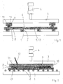
- FIG. 1 in a plan view (in the transport direction of the workpiece) illustrated device consists of a table 1 with a number of rollers 2 arranged thereon and a movable upper part 3, which can be raised and lowered by means of a fluid cylinder 4.
- a photovoltaic module 5 can be moved on the rollers 2 to drive it into the device and out of this again.
- it is not yet a photovoltaic module 5, since this consists in the current stage of the manufacturing process only of a composite of solar cells 6, which are arranged on a glass plate 13 and on their contacting elements, so usually the metallizations, each with a pastösten conductive adhesive 7 and a contact strip 8 placed thereon are provided.
- the fixation should take place so far that in later process steps in the production of the photovoltaic module, ie in particular during lamination of the same, no mechanical detachment of a contact strip 8 and / or the conductive adhesive 7 takes place and also no disturbing process gases can escape from the conductive adhesive 7 which could lead to bubbles in the later applied, important for the lamination process plastic or adhesive layer.
- FIG. 1 shown device equipped with two downholders 9, which, as FIG. 2 shows, cover the contact strips 8 substantially over the entire surface and press on the Leitkleber Mrs 7.
- the hold-down device 9 consist of a temperature-resistant above 200 ° C plastic material, and in its interior a heating element 10 is mounted in each case, which provides for a thermal basis load on the contact strip 8, for example with a temperature of 100 to 150 ° C in the contact area between the blank holder 9 and the contact strip 8.
- This temperature is with a in FIG. 2 shown temperature sensor 12 continuously measured, so that the heating element 10 can be controlled according to a predetermined set temperature.
- electrodes 11 are integrated into the hold-9, in each case in the two end regions of each contact strip 8.
- a conductive contact to the contact strip 8 can be made, so that a short-circuit current can be passed through the contact strip 8 to heat it to a temperature at which the conductive adhesive 7 is activated and optionally cured.
- the contact strip 8 heats up, ie the heat is deliberately introduced into the contact strip 8, it flows into the directly adjacent conductive adhesive 7, where it is needed. At most a fraction of this heat passes into the solar cells 6 and via the solar cells 6 in the glass plate 13, so that on the one hand, the thermal load of the solar cell 6 advantageously remains low and on the other a thermal stress in the glass plate 13 is omitted.
- the photovoltaic module of the present embodiment is a module with thin-film solar cells, which only have to be interconnected with two contact strips 8 over the width of the module.
- the intermediate solar cells 6 are already connected in series with one another, so that in the present case the two contact bands 8 are alternately heated with current pulses via the respective electrodes 11 on the right and left in order to activate the conductive adhesive layers 7.
- a typical current pulse sequence consists of several, 5 to 10 s lasting intervals with currents of about 50 to 100 A.
- the two hold-down 9 with the integrated heating elements 10 individually from the respective contact band 8 can be raised and lowered to this, the exposure time to limit the basis of the heating element 10 basic thermal load by intervals.
- the necessary for the activation of the conductive adhesive 7 heat is thus provided with an advantageously low energy consumption.
- Those elements of the module that do not necessarily have to be supplied with heat are protected in terms of their thermal load.
- a crosslinking conductive adhesive 7 by shock heating of the contact strips 8 by means of short-circuit surges in less than 60 s more than 80% crosslinking of the conductive adhesive 7 can be achieved, which is sufficient for the subsequent process steps in the rule.
- FIG. 3 also shown a separate, provided with an electrical insulation heating wire 14 between the hold-9 and the contact strip 8 and heated by passing heating current through power contacts 17. Since the heating wire 14 is provided with electrical insulation, only the heat of the heating wire 14 is transferred to the contact band 8. Current then does not flow through the contact band 8. This heating wire 14 is longer and wider than the contact strip 8, so that it is always heated completely and evenly, regardless of tolerances when placing the contact strip 8. This ensures that the ends of the contact strip 8 are securely bonded. Nevertheless, the heating wire 14 has a small cross-section to allow an accurate and flexible temperature control.
- a pulling device formed by means of two pneumatic cylinders 15 and pulleys 16 in this second embodiment keeps the heating wire 14 under tension and thus ensures that heat-related changes in length, in particular expansions of the heating wire 14 and the contact strip 8, are compensated. Since the lying under the heating wire 14 contact strip 8 is held due to mechanical friction effects together with the heating wire 14 to voltage, no wave or uneven bonding of the contact strip 8 can occur.
- the heating wire 14 has a constant and known electrical resistance, so that the contact strip 8 can be heated reproducibly, without cross-sectional tolerances of the contact strip 8 influence on the heating can have.
- the temperature of the heating wire 14 can be easily monitored and logged.
- the heating wire 14 may be formed as electrically insulated, for example, underside painted spring steel, which can be easily and quickly replaced with any contamination by adhesive residues, so that no cleaning is required.
- this heating wire 14 held on a (not shown) role and regularly be automatically clocked further to prevent contamination.
Landscapes
- Engineering & Computer Science (AREA)
- Computer Hardware Design (AREA)
- Microelectronics & Electronic Packaging (AREA)
- Power Engineering (AREA)
- Condensed Matter Physics & Semiconductors (AREA)
- Sustainable Development (AREA)
- Physics & Mathematics (AREA)
- Life Sciences & Earth Sciences (AREA)
- Electromagnetism (AREA)
- General Physics & Mathematics (AREA)
- Sustainable Energy (AREA)
- Manufacturing & Machinery (AREA)
- Photovoltaic Devices (AREA)
Applications Claiming Priority (2)
| Application Number | Priority Date | Filing Date | Title |
|---|---|---|---|
| DE200810034080 DE102008034080A1 (de) | 2008-07-21 | 2008-07-21 | Verfahren und Vorrichtung zum Verschalten von Solarzellen in einem Photovoltaikmodul |
| DE102009013524 | 2009-03-19 |
Publications (1)
| Publication Number | Publication Date |
|---|---|
| EP2148376A2 true EP2148376A2 (fr) | 2010-01-27 |
Family
ID=41323591
Family Applications (1)
| Application Number | Title | Priority Date | Filing Date |
|---|---|---|---|
| EP20090009354 Withdrawn EP2148376A2 (fr) | 2008-07-21 | 2009-07-17 | Procédé et dispositif destinés à la commutation de cellules solaires dans un module photovoltaïque |
Country Status (1)
| Country | Link |
|---|---|
| EP (1) | EP2148376A2 (fr) |
Cited By (4)
| Publication number | Priority date | Publication date | Assignee | Title |
|---|---|---|---|---|
| DE102011001673A1 (de) | 2011-03-30 | 2012-10-04 | Solarwatt Ag | Solarzelle mit metallischen Kontaktbändern |
| CN104143585A (zh) * | 2013-04-24 | 2014-11-12 | 维斯慕达有限公司 | 用于处理具有背触式体系结构的光伏面板的方法 |
| CN105352877A (zh) * | 2015-11-09 | 2016-02-24 | 江西瑞晶太阳能科技有限公司 | 一种光伏焊带的湿热检测方法 |
| CN110148581A (zh) * | 2018-02-10 | 2019-08-20 | 姜富帅 | 一种金属-半导体的金属化工艺及方法 |
-
2009
- 2009-07-17 EP EP20090009354 patent/EP2148376A2/fr not_active Withdrawn
Cited By (7)
| Publication number | Priority date | Publication date | Assignee | Title |
|---|---|---|---|---|
| DE102011001673A1 (de) | 2011-03-30 | 2012-10-04 | Solarwatt Ag | Solarzelle mit metallischen Kontaktbändern |
| DE202011110751U1 (de) | 2011-03-30 | 2016-01-27 | Solarwatt Gmbh | Solarzelle mit metallischen Kontaktbändern |
| CN104143585A (zh) * | 2013-04-24 | 2014-11-12 | 维斯慕达有限公司 | 用于处理具有背触式体系结构的光伏面板的方法 |
| CN104143585B (zh) * | 2013-04-24 | 2017-08-18 | 维斯慕达有限公司 | 用于处理具有背触式体系结构的光伏面板的方法 |
| CN105352877A (zh) * | 2015-11-09 | 2016-02-24 | 江西瑞晶太阳能科技有限公司 | 一种光伏焊带的湿热检测方法 |
| CN110148581A (zh) * | 2018-02-10 | 2019-08-20 | 姜富帅 | 一种金属-半导体的金属化工艺及方法 |
| CN110148581B (zh) * | 2018-02-10 | 2022-05-17 | 姜富帅 | 一种金属-半导体的金属化工艺及方法 |
Similar Documents
| Publication | Publication Date | Title |
|---|---|---|
| DE102016009560B4 (de) | Verfahren zur Verbesserung des ohmschen Kontaktverhaltens zwischen einem Kontaktgitter und einer Emitterschicht einer Siliziumsolarzelle | |
| EP1997614B1 (fr) | Procédé et dispositif de laminage d'éléments essentiellement en forme de plaques sous l'effet de la chaleur et de la pression | |
| DE19834459B4 (de) | Solarbatteriemodul und Verfahren für dessen Herstellung | |
| DE102008062494A1 (de) | Vorrichtung zur Erwärmung von Substraten sowie Verfahren zur Erwärmung von Substraten | |
| EP2141018A2 (fr) | Procédé et dispositif de laminage de pièces à usiner essentiellement en forme de plaques sous l'effet de la chaleur et de la pression | |
| DE2365831A1 (de) | Schichtfoermiges sicherheitsglas | |
| EP2148376A2 (fr) | Procédé et dispositif destinés à la commutation de cellules solaires dans un module photovoltaïque | |
| WO2008014900A1 (fr) | Procédé d'insertion d'un cavalier sur une cellule solaire photovoltaïque | |
| DE102008046330A1 (de) | Verfahren zum Löten von Kontaktdrähten an Solarzellen | |
| EP2390904A2 (fr) | Procédé d'interconnexion de pression à basse température de deux partenaires de liaison et agencement ainsi fabriqué | |
| EP2133923A2 (fr) | Procédé de recyclage pour modules de cellules solaires à couche fine | |
| DE102013108563A1 (de) | Verfahren und Vorrichtung zum Widerstandsschweißen von Sandwichblechen | |
| WO2016037763A1 (fr) | Dispositif d'équilibrage de température d'une unité d'alimentation en énergie électrique | |
| EP3108019B1 (fr) | Procédé de chauffage par conduction de tôles par paire et dispositif de chauffage correspondant | |
| WO2013034137A2 (fr) | Presse de formage ou dispositif de stratification | |
| WO2010083976A1 (fr) | Procédé de brasage d'un conducteur sur un support de circuit | |
| DE102008034080A1 (de) | Verfahren und Vorrichtung zum Verschalten von Solarzellen in einem Photovoltaikmodul | |
| DE102009042148B4 (de) | 14.09.2009Etagenpresse und Verfahren zur Herstellung von plattenförmigen Werkstücken | |
| EP1525900A1 (fr) | Procédé de réalisation d'un élément conducteur sur une électrode en polymère conducteur et élément obtenus à partir dudit procédé | |
| DE102010054400A1 (de) | Verfahren zur elektrischen Reihenverschaltung von Solarzellen | |
| DE102018106509B4 (de) | Verfahren und Vorrichtung zur Herstellung eines Fördergurtes mit eingebetteten Flachspulen | |
| EP2234749B1 (fr) | Procédé pour la réalisation d'une liaison brasée entre deux éléments | |
| DE102009003495C5 (de) | Lötverfahren und Lötvorrichtung | |
| DE202020103337U1 (de) | Kontakteinrichtung | |
| DE102014101489B4 (de) | Verfahren zur Herstellung einer optoelektronischen Anordnung |
Legal Events
| Date | Code | Title | Description |
|---|---|---|---|
| PUAI | Public reference made under article 153(3) epc to a published international application that has entered the european phase |
Free format text: ORIGINAL CODE: 0009012 |
|
| AK | Designated contracting states |
Kind code of ref document: A2 Designated state(s): AT BE BG CH CY CZ DE DK EE ES FI FR GB GR HR HU IE IS IT LI LT LU LV MC MK MT NL NO PL PT RO SE SI SK SM TR |
|
| AX | Request for extension of the european patent |
Extension state: AL BA RS |
|
| STAA | Information on the status of an ep patent application or granted ep patent |
Free format text: STATUS: THE APPLICATION IS DEEMED TO BE WITHDRAWN |
|
| 18D | Application deemed to be withdrawn |
Effective date: 20130201 |