EP2144373A1 - Method and apparatus for achieving 50% duty cycle on the output vco of a phased locked loop - Google Patents
Method and apparatus for achieving 50% duty cycle on the output vco of a phased locked loop Download PDFInfo
- Publication number
- EP2144373A1 EP2144373A1 EP09164251A EP09164251A EP2144373A1 EP 2144373 A1 EP2144373 A1 EP 2144373A1 EP 09164251 A EP09164251 A EP 09164251A EP 09164251 A EP09164251 A EP 09164251A EP 2144373 A1 EP2144373 A1 EP 2144373A1
- Authority
- EP
- European Patent Office
- Prior art keywords
- duty cycle
- clock signal
- transistor
- single ended
- differential
- Prior art date
- Legal status (The legal status is an assumption and is not a legal conclusion. Google has not performed a legal analysis and makes no representation as to the accuracy of the status listed.)
- Withdrawn
Links
- 238000000034 method Methods 0.000 title claims abstract description 30
- 238000005259 measurement Methods 0.000 claims abstract description 23
- 230000003321 amplification Effects 0.000 claims description 7
- 238000003199 nucleic acid amplification method Methods 0.000 claims description 7
- 239000000872 buffer Substances 0.000 claims description 5
- 230000007423 decrease Effects 0.000 description 13
- 230000000875 corresponding effect Effects 0.000 description 6
- 230000003247 decreasing effect Effects 0.000 description 6
- 239000003990 capacitor Substances 0.000 description 5
- 238000013461 design Methods 0.000 description 3
- 230000004075 alteration Effects 0.000 description 2
- 229920000729 poly(L-lysine) polymer Polymers 0.000 description 2
- 238000004458 analytical method Methods 0.000 description 1
- 238000004891 communication Methods 0.000 description 1
- 238000012937 correction Methods 0.000 description 1
- 230000002596 correlated effect Effects 0.000 description 1
- 238000004519 manufacturing process Methods 0.000 description 1
Images

Classifications
-
- H—ELECTRICITY
- H03—ELECTRONIC CIRCUITRY
- H03L—AUTOMATIC CONTROL, STARTING, SYNCHRONISATION OR STABILISATION OF GENERATORS OF ELECTRONIC OSCILLATIONS OR PULSES
- H03L7/00—Automatic control of frequency or phase; Synchronisation
- H03L7/06—Automatic control of frequency or phase; Synchronisation using a reference signal applied to a frequency- or phase-locked loop
- H03L7/08—Details of the phase-locked loop
- H03L7/099—Details of the phase-locked loop concerning mainly the controlled oscillator of the loop
-
- H—ELECTRICITY
- H03—ELECTRONIC CIRCUITRY
- H03K—PULSE TECHNIQUE
- H03K5/00—Manipulating of pulses not covered by one of the other main groups of this subclass
- H03K5/156—Arrangements in which a continuous pulse train is transformed into a train having a desired pattern
- H03K5/1565—Arrangements in which a continuous pulse train is transformed into a train having a desired pattern the output pulses having a constant duty cycle
Definitions
- the invention described herein is related to a phase-locked loop (PLL), and more particularly, to a method and apparatus for achieving a desired duty cycle on the output VCO of a PLL.
- PLL phase-locked loop
- a phase-locked loop is a control system that generates a signal having a fixed phase relationship to a reference signal.
- PLLs are widely used in radio, telecommunications, computers and other electronic applications. They may be used to generate stable frequencies, recover a signal from a noisy communication channel, or distribute clock timing pulses in digital logic designs such as microprocessors.
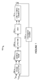
- Figure 1 depicts a typical PLL 100 with a common-mode-logic-to-CMOS (CML-to-CMOS) converter.
- the PLL 100 compares a reference signal F ref with a divided version of the clock signal F divided and adjusts the output VCO 108 based on the results of the comparison so that the clock signal F clock maintains a fixed phase relationship with the reference signal F ref .
- a common-mode-logic-to-CMOS (CML-to-CMOS) converter 110 is required to convert the CML differential voltage levels to CMOS compatible voltage levels.
- CML voltage levels represent the two values of a data bit depending on which of the two levels is higher than the other.
- a typical CMOS circuit operates according to a single ended signal with two pre-determined voltage levels defining the two values of transmitted data bits.
- the CML-to-CMOS circuit includes a limiting differential amplifier for generating a single ended clock signal from a differential common mode clock signal, where the single ended clock signal has a duty cycle, a low-pass filter for generating a measurement of the duty cycle of the single ended clock signal, and a second differential amplifier for (i) comparing the measurement with a reference voltage and (ii) generating a differential bias current signal in response to the comparison, where the differential bias current signal is applied to the limiting differential amplifier for correcting the duty cycle of the single ended clock signal to a desired duty cycle.
- the limiting differential amplifier may include a first amplification stage having a first transistor and a second transistor, wherein the differential bias current signal is applied to a first load of the first transistor and a second load of the second transistor.
- the first transistor and the second transistor may be FET transistors.
- the differential bias current signal is applied to alter a first operating point of the first FET transistor and a second operating point of the second FET transistor.
- the measurement of the duty cycle may have a single ended voltage level corresponding to the duty cycle of the single ended clock signal.
- the reference voltage defines a desired duty cycle, where the desired duty cycle may be equal to 50%. Some embodiments allow for other values of a desired duty cycle, while other allow for selection or tuning to a desired duty cycle percentage.
- the reference voltage may be generated by a voltage divider including a first resistor and a second resistor connected in series between a first voltage source and a second voltage source. According some embodiments, the reference voltage may be generated by a programmable resistor network. According to some other embodiments, the reference voltage may be generated by a digital-to-analog converter or may be provided by an external circuit.
- the CML-to-CMOS converter circuit may include at an output stage one or more buffers for inverting the single ended clock signal.
- a method for achieving a desired duty cycle on an output of a CML-to-CMOS converter.
- the method includes generating a single ended clock signal from a differential common mode clock signal using a limiting differential amplifier, wherein the single ended clock signal has a duty cycle, generating a differential bias current signal in response to the duty cycle of the single ended clock signal, and correcting the duty cycle of the single ended clock signal to a desired duty cycle by applying the differential bias current signal to the limiting differential amplifier.
- the limiting differential amplifier has a first amplification stage including a first transistor and a second transistor.
- the limiting differential amplifier has a first load provided by the first transistor and a second load provided by the second transistor.
- the first load has a first offset voltage component corresponding to a DC operating point of the first transistor and the second load has a second offset voltage component corresponding to a DC operating point of the second transistor.
- the method alters the DC operating points of the first transistor and the second transistor by applying the differential bias current signal to the first load and the second load.
- the differential bias current signal adjusts the first offset voltage component and the second offset voltage component by drawing additional currents from the first load and the second load of the limiting differential amplifier.
- the method may generate a measurement of the duty cycle of the single ended clock signal using a low-pass filter.
- the measurement has a single ended voltage level corresponding to the duty cycle of the single ended clock signal.
- the method may compare the measurement of the duty cycle of the single ended clock signal with a reference voltage.
- the reference voltage defines a desired duty cycle, where the desired duty cycle may be equal to 50%.
- Figure 1 depicts a typical PLL system with a CML-to-CMOS converter.
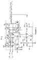
- Figure 2 depicts a CML-to-CMOS converter 200 according to one embodiment.
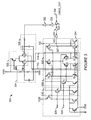
- Figure 3 depicts a CML-to-CMOS converter 300 according another embodiment.
- Figure 4 depicts a method 400 for achieving a desired duty cycle at the output of an CML-to-CMOS converter according to still another embodiment.
- FIG. 2 depicts a common-mode-logic-to-CMOS (CML-to-CMOS) converter 200 according to one embodiment.
- the CML-to-CMOS converter 200 includes a limiting differential amplifier 214 connected between a first voltage source VDD and a second voltage source VSS, a low-pass filter 224, and a differential amplifier 222.
- the CML-to-CMOS converter 200 receives a common-mode signal having components 208 and 210 and output a single ended clock signal 213.
- the components 208 and 210 of the common-mode signal may be sinusoidal wave forms, square wave forms, or other type of clock wave forms.
- the single ended clock signal 213 may be a square wave form having a duty cycle as well known in the art.
- the limiting differential amplifier 214 may include an input stage (i.e. a first amplification stage) including a differential amplifier 202 and a differential amplifier 204.
- the differential amplifier 202 has a P-MOSFET transistor Q 1 providing a first stage output 207 through the load (i.e. the drain) of the transistor Q 1 .
- the differential amplifier 204 has a P-MOSFET transistor Q 2 proving another first stage output 209 through the load (i.e. the drain) of the transistor Q 2 .
- the transistor Q 1 has a DC operating point defined by the DC voltage drop across the source and the drain and the corresponding current through the drain.
- Increasing or decreasing the current will alter the DC operating point of the transistor Q 1 and thereby alter the DC voltage drop.
- increasing the current through the drain (i.e. the load) of Q 1 may move the DC operating point away from the origin. Accordingly, the DC voltage drop across Q 1 is increased and the DC voltage level of 207 is thereby decreased.
- decreasing the current through the drain of Q 1 may move the DC operating toward the origin and thereby increase the DC voltage level of 207.
- the DC operating point of Q 2 may be altered by increasing or decreasing the current through its drain.
- the limiting differential amplifier 214 may further include an output stage 206 having transistors Q 3 , Q 4 , Q 13, and Q 14, where Q 3 and Q 4 may be P-MOSFET transistors and Q 13 and Q 14 may be N-MOSFET transistors.
- the first stage outputs 207 and 209 i.e. the loads of the first stage
- the single ended clock output 211 of the limiting differential amplifier 214 is taken from the drain of the N-MOSFET transistor Q 4 .
- a further analysis of the circuit shows that the N-MOSFET transistors Q 3 and Q 4 form a push-pull differential pair as well known in the art, providing the output clock signal 211.
- the P-MOSFET transistor pair Q 13 and Q 14 provides a current mirror that mirrors the current through the drain of Q 3 to the drain of Q 14 . Therefore, the transistors Q 3 and Q 4 operate as a push-pull differential pair, where they turn on and off alternatively, generating high and low voltage levels of the output clock signal 211.
- the transistors Q 3 and Q 4 operate as a push-pull differential pair, where they turn on and off alternatively, generating high and low voltage levels of the output clock signal 211.
- VDD e.g. a high voltage level
- Q 3 turns on and Q 4 turns off.
- output 211 is connected to the second voltage source CSS (e.g. a low voltage level) through Q 14 and, therefore, goes low.
- the limiting differential amplifier 214 may also include N-MOSFET transistors Q 9 , Q 10 , and Q 11 for generating bias currents for the input stages 202 and 204.
- the diode-connected transistor Q 9 provides control, according to the signal IB, to the transistors Q 10 and Q 11 that provide bias currents to the differential amplifiers 202 and 204.
- the limiting differential amplifier 214 may receive a power down (PD) signal through N-MOSFET transistors Q 12 and Q 15 .
- the transistors Q 12 and Q 15 provide additional benefits, as well known in the art, during the design and manufacturing of the CML-to-CMOS converter 200.
- the CML-to-CMOS converter 200 may include one or more signal buffers 212 connected to the output of the limiting differential amplifier 214.
- the one or more signal buffers 212 provide signal inversions to ensure that output signal 213 and signal 233 have desired polarities.
- the CML-to-CMOS converter 200 also includes a low pass filter 224 for generating a measurement 228 of the duty cycle of the single ended clock signal 211.
- the low pass filter 224 may be a simple analog filter including a resistor 232 and a capacitor 234. The resistor and the capacitor are chosen to convert the single ended clock signal 233 into a single ended voltage 228 representing the duty cycle of the output clock.
- the measurement voltage 228 has a single ended voltage level that increases or decreases as the duty cycle of the clock signal 233 varies. That is, the low pass filter provides an average of the voltage level, which is directly determined and correlated to the duty cycle.
- the CML-to-CMOS converter 200 may also include a reference voltage generator 216 connected between the first voltage source VDD and the second voltage source VSS.
- the reference voltage generator 216 generates a reference voltage level 227 that represents a desired duty cycle. In most PLL circuits, the desired duty cycle is 50%.
- the reference voltage generator 216 may include a voltage divider having a first capacitor 220 and a second capacitor 226 connected in series between the first voltage source VDD and the second voltage source VSS. A capacitor 230 is connected in parallel with 226 to reduce the voltage fluctuation of the reference 227.
- the reference voltage generator 216 may include a programmable resistor network or a digital-to-analog converter as well known in the art.
- the voltage generator 224 may also be applied for providing the reference voltage 227.
- the reference voltage 227 may be provided by an external circuit having a tunable voltage source.
- the reference voltage 227 may be generated off chip and provided as an input to the CML-to-CMOS converter 200.
- the CML-to-CMOS converter 200 includes another differential amplifier 222 for comparing the duty cycle measurement 228 and the reference 227 and generating a differential bias current signal having components 229 and 230 based on the comparison.
- the amplifier 222 includes an N-MOSFET transistor Q 18 receiving control signal IB for providing bias current to the differential N-MOSFET pair Q 16 and Q 17 .
- the differential amplifier 222 generates the differential bias current signal 229 and 230 by comparing the measurement 228 with the reference 227.
- the differential bias current signal components 229 and 230 are then taken from the loads (i.e. the drains) of Q 17 and Q 16 and connected, respectively, to the output 207 of the first stage amplifier 202 and the output 209 of the first stage amplifier 204.
- the components 229 and 230 of the differential bias current signal fall and rise in opposite direction. That is, as the current level of 229 increases, the current level of 230 decreases by approximately the same amount. Similarly, as the current level 229 decreases, the current level of 230 increases again by approximately the same amount.
- the method includes generating a single ended clock signal using a limiting differential amplifier.
- the limiting differential amplifier 200 receives a common mode differential signal having components 208 and 210 and generates a single ended clock signal 211 (block 402).
- the clock signal 211 is inverted one or more times by the signal buffers 212 to produce a clock signal 233 with a desired polarity.
- the clock signal 211 has a duty cycle that tends to deviate from the desired duty cycle (i.e. 50%) due to mismatches of the transistor pairs and the common mode input signal.
- the method includes generating a differential bias current signal in response to the duty cycle of the single ended clock signal 211.
- the low pass filter 224 processes the clock signal 233 and generates the measurement 228 of the duty cycle, where the voltage level of 228 represents the duty cycle of the clock signal 233.
- the differential amplifier 222 receives the measurement 228 and the reference voltage 227 generated by the reference generator as described above and generates a differential bias current signal having components 229 and 230.
- the method includes correcting the duty cycle of the single ended clock signal to a desired duty cycle by applying the differential bias current signal to the limiting differential amplifier.
- the clock signal 233 has a duty cycle lower than the desired duty cycle (i.e. 50%)
- the measurement voltage 228 decreases and becomes lower than the reference voltage 227.
- the differential current component 230 starts to draw more current from the drain of the transistor Q 2 , and thereby alters the DC operating point of the transistor Q 2 and increases the DC voltage drop across Q 2 .
- Such an increase of the DC voltage drop decreases the DC voltage level of 209 and thereby causes the transistor Q 4 to turn on earlier.
- the imbalanced inputs to the differential amplifier 222 causes the differential current component 229 to decrease the current drawn from the drain of the transistor Q 1 and thereby alters the DC operating point of Q 1 to decrease the DC voltage drop across Q 1 .
- Such a decrease of the voltage drop across Q 1 increases the voltage level of 207 and thereby causes the transistor Q 3 to turn on later.
- transistors Q 3 and Q 4 form a push-pull differential pair as described above, such an alteration the DC voltages of 207 and 209 increases the time duration in which the clock signal 211 remains high and decreases the time duration in which the clock signal 211 remains low. Consequently, the duty cycle of the clock signal 211 is increased toward the desired duty cycle.
- the measurement 228 has a voltage level greater than that of the reference 227.
- the imbalanced inputs to the differential amplifier 222 cause the differential bias current component 229 to increase and the differential bias current component 230 to decrease.
- the DC voltage level of 207 is increased and the DC voltage level of 209 is decreased.
- the transistor Q 3 turns on earlier and turns off later in time while the transistor Q 4 turns on later and turns off earlier in time.
- Such an alteration of the DC operating points of Q 1 and Q 2 causes the clock signal 211 to rise later and fall earlier in time, thereby decreasing the duty cycle toward the desired duty cycle.
- the CML-to-CMOS converter 300 receives a differential common mode clock signal having components 326 and 328 and outputs a single ended clock signal 324.
- the CML-to-CMOS converter further includes a limiting differential amplifier 334 for generating a single ended clock signal 327 from the common mode clock signal 326 and 328, a low pass filter 306 for generating a measurement 310 of the duty cycle of the single clock signal 327, and another differential amplifier 302 for comparing the measurement 310 with a reference voltage 208 and generating a differential bias current signal having components 312 and 314.
- the clock signal 327 has a duty cycle that tends to deviate from the desired duty cycle due to the mismatches of the transistor pairs and the input signals.
- the limiting differential amplifier 334 is a three-stage amplifier having first amplification stages 316 and 318, a second amplification stage 320, and an output stage including P-MOSFET transistors Q 3 and Q 5 and N-MOSFET transistors Q 10 and Q 13 .
- the transistors Q 10 and Q 13 form a push-pull differential pair through the current mirror provided by Q 3 and Q 5 , where the drain current of Q 5 is mirrored from the drain current of Q 10 .
- the differential amplifier 302 may include two P-MOSFET transistors Q 1 and Q 2 as depicted in Figure 3 .
- the differential bias current signal components 312 and 314 inject additional currents to the drains of the N-MOS transistors Q 11 and Q 12 , respectively, and thereby altering the DC operating points of the transistors Q 11 and Q 12 for correcting the duty cycle of the single ended clock signal 327 to the desired duty cycle (i.e. 50%).
- the differential amplifier 302 generates a differential bias current signal, injecting a larger current to the drain of Q 11 and a smaller current to the drain of Q 12 .
- the DC operating point of Q 11 is altered by the current component 312
- the DC voltage drop across Q 11 is increased, thereby increasing the DC voltage level of 330 and causing the transistor Q 10 to turn on earlier and turn off later in time.
- the current component 314 alters the DC operating point of Q 12 by reducing the current through the drain.
- the DC voltage level of 332 is reduced, thereby causing the transistor Q 13 to turn off earlier and turn on later in time.
- the time duration in which the clock signal 327 remains high increases while the time duration in which the clock signal 327 remains low decreases. Consequently, the differential bias current components 312 and 314 increase the duty cycle of the clock signal 327 toward the desired duty cycle (i.e. 50%).
- the measurement 310 of the duty cycle becomes higher than the reference voltage 308.
- the imbalance inputs 308 and 310 cause the differential amplifier 302 to generate a larger differential bias current component in 314 and a smaller component in 312.
- the differential bias current signal 312 and 314 inject additional currents into the drains of Q 11 and Q 12 , the operating points of these two transistors are altered. Specifically, the signal component 312 decreases the DC voltage drop across Q 11 , thereby reducing the DC voltage level of 330 and causing the transistor Q 10 to turn on later and turn off earlier in time.
- the signal component 314 increases the DC voltage drop across Q 12 , thereby increasing the DC voltage level of 332 and causing the transistor Q 13 to turn on earlier and turn off later in time. Consequently, the differential bias current signal 312 and 314 decreases the duty cycle of the clock signal 327 toward the desired duty cycle (i.e. 50%).
- the transistor pairs of the differential amplifiers 222 and 302 depicted in Figure 2 and 3 have large sizes to substantially limit the mismatch of these transistor pairs.
- the CML-to-CMOS converter 200 may have a greater operating speed than the CML-to-CMOS converter 300, while the CML-to-CMOS converter 300 may provide a more precise duty cycle correction. It may be further appreciated that the CML-to-CMOS converters 200 and 300 may be tuned to process signals in pre-determined frequency ranges. They may be utilized individually by the PLL system depicted in Figure 1 , or may be combined with other obvious variations to process signals in a broader frequency range.
Landscapes
- Physics & Mathematics (AREA)
- Nonlinear Science (AREA)
- Manipulation Of Pulses (AREA)
- Amplifiers (AREA)
- Pulse Circuits (AREA)
- Logic Circuits (AREA)
- Stabilization Of Oscillater, Synchronisation, Frequency Synthesizers (AREA)
Applications Claiming Priority (1)
| Application Number | Priority Date | Filing Date | Title |
|---|---|---|---|
| US12/171,805 US7965118B2 (en) | 2008-07-11 | 2008-07-11 | Method and apparatus for achieving 50% duty cycle on the output VCO of a phased locked loop |
Publications (1)
| Publication Number | Publication Date |
|---|---|
| EP2144373A1 true EP2144373A1 (en) | 2010-01-13 |
Family
ID=41077098
Family Applications (1)
| Application Number | Title | Priority Date | Filing Date |
|---|---|---|---|
| EP09164251A Withdrawn EP2144373A1 (en) | 2008-07-11 | 2009-06-30 | Method and apparatus for achieving 50% duty cycle on the output vco of a phased locked loop |
Country Status (3)
| Country | Link |
|---|---|
| US (1) | US7965118B2 (enExample) |
| EP (1) | EP2144373A1 (enExample) |
| JP (1) | JP2010028809A (enExample) |
Cited By (1)
| Publication number | Priority date | Publication date | Assignee | Title |
|---|---|---|---|---|
| CN108037345A (zh) * | 2017-09-27 | 2018-05-15 | 北京集创北方科技股份有限公司 | 信号处理方法、装置、存储介质和处理器 |
Families Citing this family (10)
| Publication number | Priority date | Publication date | Assignee | Title |
|---|---|---|---|---|
| US7839195B1 (en) * | 2009-06-03 | 2010-11-23 | Honeywell International Inc. | Automatic control of clock duty cycle |
| US20120154021A1 (en) * | 2010-12-20 | 2012-06-21 | Amita Chandrakant Patil | Integrated circuit and method of fabricating same |
| KR20130096495A (ko) | 2012-02-22 | 2013-08-30 | 삼성전자주식회사 | 반도체 장치의 버퍼 회로 |
| US9148135B2 (en) * | 2012-06-26 | 2015-09-29 | Taiwan Semiconductor Manufacturing Co., Ltd. | Real time automatic and background calibration at embedded duty cycle correlation |
| US8872562B2 (en) * | 2013-03-21 | 2014-10-28 | Kabushiki Kaisha Toshiba | Semiconductor device |
| US9019014B2 (en) * | 2013-07-29 | 2015-04-28 | King Fahd University Of Petroleum And Minerals | Programmable multi-gain current amplifier |
| US9007096B1 (en) * | 2014-07-07 | 2015-04-14 | Xilinx, Inc. | High-speed analog comparator |
| US9614527B2 (en) * | 2014-09-04 | 2017-04-04 | Fujitsu Limited | Differential to single-ended signal conversion |
| US11165431B1 (en) * | 2020-12-09 | 2021-11-02 | Analog Devices, Inc. | Techniques for measuring slew rate in current integrating phase interpolator |
| CN115603710A (zh) * | 2022-10-25 | 2023-01-13 | 四川和芯微电子股份有限公司(Cn) | 占空比校正电路 |
Citations (3)
| Publication number | Priority date | Publication date | Assignee | Title |
|---|---|---|---|---|
| US6169434B1 (en) * | 1997-09-05 | 2001-01-02 | Rambus Inc. | Conversion circuit with duty cycle correction for small swing signals, and associated method |
| US20050225370A1 (en) * | 2004-04-08 | 2005-10-13 | Infineon Technologies Ag | Circuit arrangement for regulating a parameter of an electrical signal |
| US20070132494A1 (en) * | 2005-12-13 | 2007-06-14 | Yang Ki Kim | Duty cycle correction amplification circuit |
Family Cites Families (18)
| Publication number | Priority date | Publication date | Assignee | Title |
|---|---|---|---|---|
| US4437171A (en) * | 1982-01-07 | 1984-03-13 | Intel Corporation | ECL Compatible CMOS memory |
| US4496856A (en) * | 1982-07-21 | 1985-01-29 | Sperry Corporation | GaAs to ECL level converter |
| US4533842A (en) * | 1983-12-01 | 1985-08-06 | Advanced Micro Devices, Inc. | Temperature compensated TTL to ECL translator |
| US4656375A (en) * | 1985-12-16 | 1987-04-07 | Ncr Corporation | Temperature compensated CMOS to ECL translator |
| US4968905A (en) * | 1989-08-25 | 1990-11-06 | Ncr Corporation | Temperature compensated high speed ECL-to-CMOS logic level translator |
| JP2549743B2 (ja) * | 1990-03-30 | 1996-10-30 | 株式会社東芝 | 出力回路 |
| US5034635A (en) * | 1990-03-30 | 1991-07-23 | Texas Instruments Incorporated | Positive to negative voltage translator circuit and method of operation |
| JPH07183775A (ja) * | 1993-12-22 | 1995-07-21 | Kawasaki Steel Corp | 波形整形回路 |
| WO1995022202A1 (en) * | 1994-02-15 | 1995-08-17 | Rambus, Inc. | Amplifier with active duty cycle correction |
| US6104229A (en) * | 1996-05-02 | 2000-08-15 | Integrated Device Technology, Inc. | High voltage tolerable input buffer and method for operating same |
| JP3745517B2 (ja) * | 1997-10-20 | 2006-02-15 | 富士通株式会社 | タイミング回路 |
| JP3745123B2 (ja) * | 1998-08-24 | 2006-02-15 | 三菱電機株式会社 | デューティ比補正回路及びクロック生成回路 |
| US6535017B1 (en) * | 2001-12-20 | 2003-03-18 | Honeywell International Inc. | CMOS ECL input buffer |
| US6563342B1 (en) * | 2001-12-20 | 2003-05-13 | Honeywell International, Inc. | CMOS ECL output buffer |
| GB0413152D0 (en) * | 2004-06-14 | 2004-07-14 | Texas Instruments Ltd | Duty cycle controlled CML-CMOS converter |
| US7345931B2 (en) * | 2005-08-01 | 2008-03-18 | Infineon Technologies Ag | Maintaining internal voltages of an integrated circuit in response to a clocked standby mode |
| US20070159224A1 (en) * | 2005-12-21 | 2007-07-12 | Amar Dwarka | Duty-cycle correction circuit for differential clocking |
| US7688110B2 (en) * | 2008-01-07 | 2010-03-30 | Honeywell International, Inc. | System for providing a complementary metal-oxide semiconductor (CMOS) emitter coupled logic (ECL) equivalent input/output (I/O) circuit |
-
2008
- 2008-07-11 US US12/171,805 patent/US7965118B2/en active Active
-
2009
- 2009-06-30 EP EP09164251A patent/EP2144373A1/en not_active Withdrawn
- 2009-07-08 JP JP2009161829A patent/JP2010028809A/ja active Pending
Patent Citations (3)
| Publication number | Priority date | Publication date | Assignee | Title |
|---|---|---|---|---|
| US6169434B1 (en) * | 1997-09-05 | 2001-01-02 | Rambus Inc. | Conversion circuit with duty cycle correction for small swing signals, and associated method |
| US20050225370A1 (en) * | 2004-04-08 | 2005-10-13 | Infineon Technologies Ag | Circuit arrangement for regulating a parameter of an electrical signal |
| US20070132494A1 (en) * | 2005-12-13 | 2007-06-14 | Yang Ki Kim | Duty cycle correction amplification circuit |
Cited By (2)
| Publication number | Priority date | Publication date | Assignee | Title |
|---|---|---|---|---|
| CN108037345A (zh) * | 2017-09-27 | 2018-05-15 | 北京集创北方科技股份有限公司 | 信号处理方法、装置、存储介质和处理器 |
| CN108037345B (zh) * | 2017-09-27 | 2020-08-04 | 北京集创北方科技股份有限公司 | 信号处理方法、装置、存储介质和处理器 |
Also Published As
| Publication number | Publication date |
|---|---|
| JP2010028809A (ja) | 2010-02-04 |
| US7965118B2 (en) | 2011-06-21 |
| US20100007393A1 (en) | 2010-01-14 |
Similar Documents
| Publication | Publication Date | Title |
|---|---|---|
| US7965118B2 (en) | Method and apparatus for achieving 50% duty cycle on the output VCO of a phased locked loop | |
| US8154352B2 (en) | Oscillating circuit | |
| EP0829135B1 (en) | Phase shifting circuit and method for providing a phase shift | |
| US6643790B1 (en) | Duty cycle correction circuit with frequency-dependent bias generator | |
| US7592877B2 (en) | Variable frequency oscillator and communication circuit with it | |
| US7432752B1 (en) | Duty cycle stabilizer | |
| US8248130B2 (en) | Duty cycle correction circuit | |
| US11218152B2 (en) | Charge pump circuit and phase-locked loop | |
| US8773186B1 (en) | Duty cycle correction circuit | |
| US7847607B2 (en) | PLL circuit | |
| KR100534211B1 (ko) | 반도체 장치에 있어서의 듀티 사이클 보정회로 | |
| US8816782B2 (en) | Phase locked loop circuit having a voltage controlled oscillator with improved bandwidth | |
| US10623005B2 (en) | PLL circuit and CDR apparatus | |
| US8384457B2 (en) | Duty cycle correction | |
| US10547315B2 (en) | Frequency divider and a transceiver including the same | |
| US8508304B2 (en) | Serdes VCO with phased outputs driving frequency to voltage converter | |
| CN101425803A (zh) | 环路压控振荡器 | |
| CN109842410B (zh) | 分频器和包括该分频器的收发器 | |
| US7642867B2 (en) | Simple technique for reduction of gain in a voltage controlled oscillator | |
| US7834709B2 (en) | Circuit for voltage controlled oscillator | |
| Moazedi et al. | A highly-linear modified pseudo-differential current starved delay element with wide tuning range | |
| US10554199B2 (en) | Multi-stage oscillator with current voltage converters | |
| US7750744B2 (en) | Single-ended to differential translator to control current starved delay cell bias | |
| JP7119757B2 (ja) | パルス位置変調回路及び送信回路 | |
| KR20050028172A (ko) | 고속 전압 제어 발진기 |
Legal Events
| Date | Code | Title | Description |
|---|---|---|---|
| PUAI | Public reference made under article 153(3) epc to a published international application that has entered the european phase |
Free format text: ORIGINAL CODE: 0009012 |
|
| 17P | Request for examination filed |
Effective date: 20090630 |
|
| AK | Designated contracting states |
Kind code of ref document: A1 Designated state(s): AT BE BG CH CY CZ DE DK EE ES FI FR GB GR HR HU IE IS IT LI LT LU LV MC MK MT NL NO PL PT RO SE SI SK TR |
|
| STAA | Information on the status of an ep patent application or granted ep patent |
Free format text: STATUS: THE APPLICATION IS DEEMED TO BE WITHDRAWN |
|
| 18D | Application deemed to be withdrawn |
Effective date: 20150106 |