EP2144271A1 - Röntgenbildgebungsvorrichtung und röntgengerät - Google Patents
Röntgenbildgebungsvorrichtung und röntgengerät Download PDFInfo
- Publication number
- EP2144271A1 EP2144271A1 EP08751624A EP08751624A EP2144271A1 EP 2144271 A1 EP2144271 A1 EP 2144271A1 EP 08751624 A EP08751624 A EP 08751624A EP 08751624 A EP08751624 A EP 08751624A EP 2144271 A1 EP2144271 A1 EP 2144271A1
- Authority
- EP
- European Patent Office
- Prior art keywords
- ray
- imaging device
- light
- detection section
- section
- Prior art date
- Legal status (The legal status is an assumption and is not a legal conclusion. Google has not performed a legal analysis and makes no representation as to the accuracy of the status listed.)
- Granted
Links
Images




Classifications
-
- G—PHYSICS
- G01—MEASURING; TESTING
- G01T—MEASUREMENT OF NUCLEAR OR X-RADIATION
- G01T1/00—Measuring X-radiation, gamma radiation, corpuscular radiation, or cosmic radiation
- G01T1/16—Measuring radiation intensity
- G01T1/24—Measuring radiation intensity with semiconductor detectors
- G01T1/246—Measuring radiation intensity with semiconductor detectors utilizing latent read-out, e.g. charge stored and read-out later
-
- H—ELECTRICITY
- H01—ELECTRIC ELEMENTS
- H01J—ELECTRIC DISCHARGE TUBES OR DISCHARGE LAMPS
- H01J31/00—Cathode ray tubes; Electron beam tubes
- H01J31/08—Cathode ray tubes; Electron beam tubes having a screen on or from which an image or pattern is formed, picked up, converted, or stored
- H01J31/26—Image pick-up tubes having an input of visible light and electric output
- H01J31/28—Image pick-up tubes having an input of visible light and electric output with electron ray scanning the image screen
-
- H—ELECTRICITY
- H01—ELECTRIC ELEMENTS
- H01J—ELECTRIC DISCHARGE TUBES OR DISCHARGE LAMPS
- H01J31/00—Cathode ray tubes; Electron beam tubes
- H01J31/08—Cathode ray tubes; Electron beam tubes having a screen on or from which an image or pattern is formed, picked up, converted, or stored
- H01J31/49—Pick-up adapted for an input of electromagnetic radiation other than visible light and having an electric output, e.g. for an input of X-rays, for an input of infrared radiation
-
- H—ELECTRICITY
- H04—ELECTRIC COMMUNICATION TECHNIQUE
- H04N—PICTORIAL COMMUNICATION, e.g. TELEVISION
- H04N23/00—Cameras or camera modules comprising electronic image sensors; Control thereof
- H04N23/30—Cameras or camera modules comprising electronic image sensors; Control thereof for generating image signals from X-rays
-
- H—ELECTRICITY
- H10—SEMICONDUCTOR DEVICES; ELECTRIC SOLID-STATE DEVICES NOT OTHERWISE PROVIDED FOR
- H10F—INORGANIC SEMICONDUCTOR DEVICES SENSITIVE TO INFRARED RADIATION, LIGHT, ELECTROMAGNETIC RADIATION OF SHORTER WAVELENGTH OR CORPUSCULAR RADIATION
- H10F30/00—Individual radiation-sensitive semiconductor devices in which radiation controls the flow of current through the devices, e.g. photodetectors
- H10F30/301—Individual radiation-sensitive semiconductor devices in which radiation controls the flow of current through the devices, e.g. photodetectors the devices being sensitive to very short wavelength, e.g. being sensitive to X-rays, gamma-rays or corpuscular radiation
-
- H—ELECTRICITY
- H10—SEMICONDUCTOR DEVICES; ELECTRIC SOLID-STATE DEVICES NOT OTHERWISE PROVIDED FOR
- H10F—INORGANIC SEMICONDUCTOR DEVICES SENSITIVE TO INFRARED RADIATION, LIGHT, ELECTROMAGNETIC RADIATION OF SHORTER WAVELENGTH OR CORPUSCULAR RADIATION
- H10F39/00—Integrated devices, or assemblies of multiple devices, comprising at least one element covered by group H10F30/00, e.g. radiation detectors comprising photodiode arrays
- H10F39/10—Integrated devices
- H10F39/12—Image sensors
- H10F39/191—Photoconductor image sensors
- H10F39/195—X-ray, gamma-ray or corpuscular radiation imagers
Definitions
- the present invention relates to an X-ray imaging device suitable for X-ray photography in a medical diagnostic field such as for medical department and dental department.
- Fig. 13 shows a conventional X-ray imaging device 101 suitable for X-ray photography in the medical diagnostic field.
- the X-ray imaging device 101 includes an X-ray conversion layer 102 made of an X-ray converter material including amorphous selenium (a-Se) and a thin-film transistor (TFT) array 103.
- An incident X-ray is converted into electric charges in the X-ray conversion layer 102, and the electric charges are read by the TFT array 103 to provide an X-ray image.
- Such devices as the X-ray imaging device 101 are disclosed in Patent Literature 1 and Nonpatent Literature 1.
- the detection efficiency or sensitivity of an X-ray image in the X-ray imaging device depends on the amount of charges produced by converting an X-ray in the X-ray conversion layer.
- the amount of energy detectable as an image is only about 70% at the maximum of the total X-ray energy incident into the surface of the X-ray imaging devices.
- the X-ray photography in the medical diagnosis field is strongly required to reduce the exposure of a subject. Therefore, it is most important for the X-ray imaging devices applied to the medical diagnosis field to find the solution to a problem of how to enhance the sensitivity in order to reduce the exposure of a subject.
- Patent Literature 1 JP2001-148475 A Nonpatent Literature 1: Yoshihiro Izumi et al, "Development of Flat Panel X-Ray Image Sensor", Sharp Technical Report No. 80, P25 - P30, August 2001, Sharp Co., Ltd.
- An object of the present invention is to provide an X-ray imaging device with substantially enhanced sensitivity particularly in order to considerably reduce the exposure of a subject at the time of X-ray photography in the medical diagnosis field.
- X-ray is used to refer to electromagnetic waves generated by change of state of electrons in an atom, the electromagnetic waves including at least those having a wavelength of approximately 1pm to 10nm.
- a first aspect of the present invention provides an X-ray imaging device, comprising: an X-ray detection section including an X-ray conversion layer having a first surface into which an X-ray enters and a second surface opposite to the first surface and made of an X-ray converter material for generating electric charges upon incidence of the X-ray, a first charge injection blocking layer formed on the first surface of the X-ray conversion layer, and a second charge injection blocking layer formed on the second surface of the X-ray conversion layer; a cold electron source having a plurality of electron emission sections arranged in a matrix form, each of the electronic emission sections being capable of emitting electrons toward the second charge injection blocking layer of the X-ray detection section; a light-shielding section for shielding visible light from entering into the X-ray detection section; a voltage application section for applying a voltage to the X-ray conversion layer of the X-ray detection section to generate an electric field which induces avalanche multiplication; an electron source drive section for driving a plurality of
- X-ray conversion layer of the X-ray detection section electric charges generated by the incidence of an X-ray are multiplied by avalanche multiplication.
- the incidence of visible light into the X-ray detection section is blocked by the light-shielding section. Therefore, with this configuration, X-ray image applied to the X-ray detection section can be electronically detected as an image data with extremely high sensitivity without an influence of disturbance by visible light and the like, achieving considerable reduction in the exposure of a subject in the X-ray photography in the medical diagnosis field.
- the X-ray converter material includes amorphous selenium for example.
- Amorphous selenium already has been widely used as a photoelectric conversion material which converts visible light into an electric charge. Accordingly, using amorphous selenium as the X-ray converter material for the X-ray conversion layer enables application of known manufacturing methods, resulting in easy implementation of a high sensitivity X-ray imaging device.
- a ballistic electron surface-emitting device can be employed as the cold electron source.
- NPS layer Nanocrystalline Poly-Silicon Layer
- the ballistic electron surface-emitting device Used as the ballistic electron surface-emitting device is a Nanocrystalline Poly-Silicon Layer (NPS layer) formed like a film, which is structured to have a large number of fine chain-shaped structures made of nanocrystalline silicon layers and placed between pillar-shaped polysilicon structures. Since the NPS layer can be manufactured by applying anodising and low-temperature oxidation process to the polysilicon layer, upsizing can easily be achieved. Therefore, employing the ballistic electron surface-emitting device can achieve a large-area X-ray imaging device having a large imaging region.
- NPS layer Nanocrystalline Poly-Silicon Layer
- a Spindt-type electron source can be employed as the cold electron source.
- the density of an emitter which functions as an electron emission section can be increased with the Spindt-type electron source being used as a cold electron source, an image of higher fineness can be provided by the X-ray imaging device.
- the light-shielding section is a light-shielding coating layer made of a light-shielding resin material, the light-shielding coating layer being formed so as to cover at least a side of the X-ray detection section which is the first surface side into which the X-ray enters.
- the light-shielding section may be a light-shielding casing made of a light-shielding material for housing at least the X-ray detection section and the cold electron source therein.
- the voltage application section favorably generates an average electric field of between 0.1x10 6 V/m and 0.6x10 6 V/m in the X-ray conversion layer of the X-ray detection section.
- the X-ray imaging device can be controlled with high sensitivity and with practical operating voltage.
- a second aspect of the invention provides an X-ray radiographic apparatus, comprising: the above-mentioned X-ray imaging device; a moving section for spatially moving the X-ray imaging device; and an X-ray irradiation section placed on an opposite side of the X-ray imaging device with respect a photographing target for irradiating the photographing target with an X-ray and making the transmitted X-ray enter into the imaging device.
- This configuration can achieve a practical X-ray radiographic apparatus which can perform X-ray photography with high sensitivity while moving an X-ray imaging device spatially.
- the X-ray radiographic apparatus allows considerable reduction in the exposure of a subject.
- the X-ray detection section which includes charge injection blocking layers formed on both the sides of the X-ray conversion layer made of an X-ray converter material, the cold electron source having a plurality of electron emission sections placed in a matrix form, and the light-shielding section for shielding incidence of visible light
- a X-ray imaging device with extremely high sensitivity without being influenced by disturbance by visible light and the like can be achieved. Applying the X-ray imaging device to the X-ray photography in the medical diagnosis field allows considerable reduction in the exposure of a subject at the time of photographing.
- 1 X-ray imaging device; 2: X-ray detection section; 3: cold electron source; 4: face plate; 5: base plate; 6: side plate; 7: device casing; 8: vacuum space; 9: light-shielding coating layer; 11: insulating layer; 12: electrode layer; 13: X-ray conversion layer; 13a: incidence surface; 13b: rear surface; 14: first charge injection blocking layer; 15: second charge injection blocking layer; 16: conductive line; 17: voltage application circuit; 18: readout circuit; 19: amplification circuit; 20: A/D conversion circuit; 23: electron source drive circuit; 31: Ballistic electron Surface-emitting Device (BSD); 32: Poly-Silicon Layer (NPS layer); 32a: electron emission surface; 32b: rear surface; 33: upper electrode; 34: lower electrode; 35: substrate; 36: pillar-shaped polysilicon; 37: nanocrystalline polysilicon, 38A, 38B: strip electrode; 39: ground; 40: switching circuit; 41: voltage application circuit; 42: electrode; 43: voltage
- Figs. 1 and 2 show an X-ray imaging device 1 according to a first embodiment of the invention.
- the X-ray imaging device 1 includes an X-ray detection section 2, a cold electron source 3, and a light-shielding coating layer 9.
- the X-ray detection section 2 is formed on a face plate 4 made of aluminum, glass and the like, while the cold electron source 3 is formed on a base plate 5 placed with a distance from the face plate 4.
- the face plate 4 and the base plate 5 may be made of any material including aluminum and glass.
- a side plate 6 which is made of such materials as ceramics is provided between the face plate 4 and the base plate 5.
- the face plate 4, the base plate 5, and the side plate 6 constitute a device casing 7.
- the device casing 7 accommodates the X-ray detection section 2 and the cold electron source 3 therein.
- the X-ray detection section 2 and the cold electron source 3 are opposed to each other with a vacuum space 8 interposed therebetween in the device casing 7.
- An insulating layer 11 and an electrode layer 12 which is made of indium tin oxide (ITO) and the like are provided between the X-ray detection section 2 and the face plate 4.
- An X-ray enters into the X-ray detection section 2 from the face plate 4 side.
- the X-ray detection section 2 has an X-ray conversion layer 13 which is made of an X-ray converter material including amorphous selenium (a-Se).
- the X-ray converter material is not limited to amorphous selenium and may be cadmium tellurium (CdTe) or other materials.
- a first charge injection blocking layer 14 which is made of cerium oxide (Ce02) is formed on an incidence surface (first surface) 13a of the X-ray conversion layer 13 into which an X-ray enters.
- a second charge injection blocking layer 15 which is made of antimony trisulfides (Sb 2 S 3 ) is formed on the rear surface (second surface) 13b of the X-ray conversion layer 13 on the opposite side of the incidence surface 13a.
- the X-ray detection section 2 is known as HARP (High-gain Avalanche Rushing amorphous Photoconductor) in the field of imaging of visible light.
- the electrode layer 12 is electrically connected to a conductive line 16, via which voltage is supplied from a voltage application circuit 17.
- the conductive line 16 is also connected to an amplification circuit 19 and an A/D conversion circuit 20 via a readout circuit 18.
- Figs. 1 and 2 schematically show the cold electron source 3.
- the specific configuration of the cold electron source 3 will be described later in detail with reference to Figs. 3 to 8 .
- the cold electron source 3 has a large number of electron emission sections 3a which can emit electrons toward the X-ray detection section 2. A large number of these electron emission sections 3a are arranged in an array or a matrix form seen from the incidence direction of the X-ray.
- An electron source drive circuit 23 sequentially drives the electron emission sections 3a so that electrons are emitted.
- the specific configuration of the electron source drive circuit 23 will also be described later in detail.
- a light-shielding coating layer 9 is formed to cover the surface (upper surface in Fig. 1 ) of the face plate 4, the surface being opposite to the surface having the X-ray detection section 2 formed thereon, and also covers the external surface of the side plate 6 so that the inside of the device casing 7 is sealed.
- the light-shielding coating layer 9 is made of a light-shielding resin which transmits an X-ray but shields visible light. This kind of light-shielding-resin material includes, for example, black urethane resin and silicon resin.
- the light-shielding coating layer 9 needs to cover at least the incidence surface side of the X-ray detection section 2.
- Selection of the light-shielding resin material used as the light-shielding coating layer 9 and the thickness of the light-shielding coating layer 9 need to be so set as to ensure that incidence of the visible light into the X-ray detection section 2 is shielded.
- pairs of electrons and electron holes corresponding to the dose of an X-ray which passed the first charge injection blocking layer 14 and entered into the X-ray converter material, are generated inside the X-ray converter material which constitutes the X-ray conversion layer 13.
- the generated electron holes are accelerated by an intense electric field applied to the X-ray detection section 2 by the voltage application circuit 17, and collide in sequence with atoms within the X-ray converter material to produce new pairs of electrons and electron holes like avalanche, resulting in multiplication of the number of pairs of electrons and electron holes. This phenomenon is known as avalanche multiplication.
- the avalanche multiplication forms positive charge patterns multiplied tenfold or more in proportion to the incident X-ray image on the rear surface 13b (cold electron source 3 side) of the X-ray conversion layer 13.
- the voltage applied by the voltage application circuit 17 to the X-ray detection section 2 needs to be set so that an electric field is generated with intensity sufficient for the avalanche multiplication to occur in the X-ray conversion layer 13.
- Practical use of the avalanche multiplication phenomenon is found in an ultrahigh sensitivity imaging camera (so-called High-gain Avalanche Rushing amorphous Photoconductor (HARP) camera) with use of photoelectric conversion materials in the field of visible light, the HARP camera being reported to have photographing sensitivity of 10 times or more of the usual CCD camera.
- the X-ray detection section 2 is covered with the light-shielding coating layer 9 so as to prevent incidence of the visible light into the X-ray converter material, and therefore an influence of the visible light at the time of X-ray image detection can be prevented. As a result, it becomes possible to prevent the influence of the visible light at the time of X-ray photography, resulting in sufficient X-ray image with less disturbance.
- Electrons are emitted from the electron emission sections 3a of the cold electron source 3 toward the X-ray detection section 2 (rear surface 13b of the X-ray conversion layer 13). These electrons and the electron holes generated within the X-ray conversion layer 13 face each other across the second charge injection blocking layer 15, and the level of electric charges neutralized therebetween is electronically detected, so that image signals representing the X-ray image are loaded onto the readout circuit 18. More specifically, a large number of the electron emission sections 3a arranged in a matrix form as mentioned before are sequentially driven to emit electrons, so that the level of electric charges generated by X-ray irradiation is serially read one by one in every area (pixel) corresponding to the respective electron emission sections 3a of the X-ray conversion layer 13. In other words, the charge pattern generated in the X-ray conversion layer 13 is scanned by sequentially driving the electron emission sections 3a of the cold electron source 3.
- the X-ray conversion layer 13 of the X-ray detection section 2 electric charges generated by the incidence of an X-ray are multiplied by avalanche multiplication as mentioned before. Moreover, the incidence of visible light into the X-ray detection section 2 is shielded by the light-shielding coating layer 9. Therefore, in the X-ray imaging device in this embodiment, it becomes possible to electronically detect an X-ray image applied to the X-ray detection section 2 as image data with extremely high sensitivity without an influence of disturbance by visible light and the like. Applying the X-ray imaging device 1 of this embodiment to X-ray photography in the medical diagnosis field allows drastic reduction in the X-ray dosage applied to a subject, as a result of which the exposure of the subject can be reduced.
- the light-shielding coating layer 9 which is made of light-shielding resin material. Accordingly, the visible light can be blocked with a relatively easy step. Moreover, sufficient sealability within the device casing 7, as well as high moisture resistance and durability are achieved.
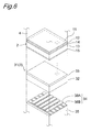
- Figs. 3 to 6 show the more specific configuration of the X-ray imaging device 1 of this embodiment with a Ballistic electron Surface-emitting Device (BSD) 31 employed as the cold electron source 3.
- BSD Ballistic electron Surface-emitting Device
- the BSD 31 includes a Nanocrystalline Poly-Silicon Layer (NPS layer) 32, a upper electrode 33 which is constituted of a single thin film made of metal such as gold and which is formed on the electronic emission surface 32a side of the NPS layer 32, and a lower electrode 34 formed on a rear surface 32b opposite to the electronic emission surface 32a.
- the BSD 31 is formed on a substrate 35 made of glass and the like.
- the NPS layer 32 is formed like a film, which is structured to have a large number of fine chain-shaped structures made of nanocrystalline polysilicons 37, each having a diameter of about 5nm, and formed between pillar-shaped polysilicons 36.
- Each surface of the pillar-shaped polysilicons 36 and the nanocrystalline polysilicons 37 is covered with an oxide 45 made of SiO 2 and the like.
- the lower electrode 34 has a plurality of strip electrodes 38A placed in a row direction with a distance from each other and a plurality of strip electrodes 38B extending in a column direction orthogonal to these strip electrodes 38A.
- Areas of the NPS layer 32 located between intersections of two kinds of electrodes, the strip electrodes 38A and 38B, and the upper electrode 33 function as electron emission sections 3a as shown in Figs. 1 and 2 .
- the electron source drive circuit 23 has a switching circuit 40 in order to sequentially connect the intersections of the strip electrodes 38A and 38B, which constitute the lower electrode 34, to a ground 39. In other words, the switching circuit 40 executes the address of each pixel.
- the electron source drive circuit 23 includes a voltage application circuit 43 which applies voltage to the upper electrode 33 of the BSD 31.
- the BSD 31 formed on the substrate 35 such as glass has an advantage that an electron source having larger area than other cold electron sources formed on a semiconductor substrate can be achieved.
- employing a BSD as the cold electron source makes it easy to achieve the high-sensitivity X-ray imaging device 1 of this embodiment to have a larger area without being influenced by the disturbance by visible light and the like as described before, resulting in increased practical use of the X-ray imaging device 1 for X-ray photography in the medical imaging field in particular.
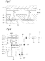
- Figs. 7 and 8 show the more specific configuration of the X-ray imaging device 1 in this embodiment with a Spindt-type electron source 51, which is a cold cathode field emission-type electron source, being employed as the cold electron source 3.
- a Spindt-type electron source 51 which is a cold cathode field emission-type electron source, being employed as the cold electron source 3.
- component members similar to those in Figs. 3 to 6 are designated by similar reference signs.
- the Spindt-type electron source 51 has a plurality of belt-like cathode electrodes 53 formed on a substrate 52 which is made of glass and the like, and a plurality of belt-like gate electrodes 55 formed on the cathode electrodes 53 with an insulating layer 54, which is made of SiO 2 and the like, interposed therebetween.
- a large number of fine pores 56 are formed in the gate electrode 55 and the insulating layer 54.
- an emitter 57 having a sharpened tip part protruding from the cathode electrode 53 is provided.
- the cathode electrodes 53 and the gate electrodes 55 extend in the direction orthogonal to each other, and intersections between the cathode electrodes 53 and the gate electrode 55 function as electron emission sections 3a as shown in Figs. 1 and 2 .
- the number of emitters 57 included in the intersection of each cathode electrode 53 and gate electrode 55 may be any number as long as it is one or more.
- the switching circuit 40 sequentially switches a voltage applied to between the cathode electrode 53 and the gate electrodes 55 from the voltage application circuit 43, by which the address of each pixel is executed.
- the electrode 42 is a grid-like or mesh-like electrode for accelerating the electrons, and voltage is applied thereto by the voltage application circuit 41.
- the electrons emitted from the emitter 57 reaches the second charge injection blocking layer 15 of the X-ray detection section 2 through the electrode 42.
- the Spindt-type electron source 51 can be manufactured by a semiconductor device manufacturing technology, very fine processing can be applied thereto, so that a large number of electron source elements can be formed with high density. Therefore, employing the Spindt-type electron source 51 as a cold electron source makes it possible to form the electron source element, which constitutes a pixel in X-ray photography, with high density, so that a very high definition X-ray photography image can be provided.
- An X-ray imaging device 1 according to the second embodiment of the invention shown in Fig. 9 is different from the first embodiment in the configuration of shielding visible light from entering into the X-ray detection section 2. More specifically, in this embodiment, the X-ray imaging device 1 is accommodated in a light-shielding casing 61 which is made of a light-shielding material. As the light-shielding material, such materials as beryllium, ceramics and aluminum can be used for example. Employing the light-shielding casing 61 facilitates disassembly and repair of the X-ray imaging device 1. Moreover, X-ray filters and the like can easily be detached and replaced according to photographing conditions such as X-ray intensity.
- An X-ray imaging device 1 according to the third embodiment of the invention shown in Fig. 10 is also different from the first embodiment in the configuration of shielding visible light from entering into the X-ray detection section 2. More specifically, a device casing 7 itself of the X-ray imaging device 1 is provided with a light shielding effect in this embodiment. More specifically, a face plate 4, a base plate 5 and a side plate 6, which constitute the device casing 7, are all made of materials which transmit an X-ray but block visible light. For example, the face plate 4 and the base plate 5 may be made of aluminum, and the side plate 6 may be made of ceramics.
- a voltage value applied to the X-ray detection section 2 of the X-ray imaging device 1 will be explained in detail. It is necessary to generate an electric field with intensity high enough to induce avalanche multiplication in the X-ray conversion layer 13 of the X-ray detection section 2 as mentioned before. Therefore, the voltage value applied to the X-ray detection section 2 by the voltage application circuit 17 needs at least to fulfill this condition. Particularly, it is preferable to set the voltage value applied to the X-ray detection section 2 by the voltage application circuit 17 so that an average electric field of between 0.1x10 8 V/m and 0.6x10 8 V/m is generated in the X-ray detection section 2. The reason thereof will be described below.
- Fig. 11 is a characteristic diagram showing change in signal current and change in magnification with respect to applied voltage to the X-ray detection section 2 in the X-ray imaging device 1 of the invention.
- a region "a" represents a range of an average electric field of between 0.1x10 8 V/m and 0.6x10 8 V/m
- a region "b” represents a range of an average electric field over 0.6x10 8 V/m.
- a multiplication factor of an output signal changes depending on the intensity of an average electric field, and a signal current increases rapidly in the region "b" where the average electric field exceeds 0.6x10 8 V/m. This is because the effect of the avalanche multiplication phenomenon becomes noticeable.
- ultrahigh sensitivity imaging camera for visible light HTP camera
- the multiplication factor of about tenfold or more and twentyfold or less is secured although it is lower than that of the region "b".
- the multiplication factor of the region "b" is a value which can implement sufficiently high sensitivity.
- the region "a" has extremely small change in the multiplication factor with respect to the change in the average field intensity.
- the multiplication factor of tenfold or more and twentyfold or less can be obtained and stable multiplication can be achieved without high-precision control on applied voltage.
- the X-ray imaging device 1 of the invention is used in the applied voltage range in which the average field intensity of the X-ray detection section 2 is within the range of the region "a"
- the X-ray imaging device 1 can be controlled with practical operating voltage while high sensitivity is secured.
- Fig. 12 shows an X-ray radiographic apparatus 71 for dentistry as an example of a medical X-ray radiographic apparatus having the X-ray imaging device 1 of the invention.
- the X-ray radiographic apparatus 71 for dentistry has a rotary arm (moving section) 73 having an irradiation section 73a and an image pickup section 73b which face each other across a head 72 of a subject that is a photographing target.
- the rotary arm 73 rotates around an axis extending in a perpendicular direction as shown by an arrow in Fig. 11 by an unshown drive mechanism.
- the irradiation section 73a has an X-ray source 74.
- the image pickup section 73b is equipped with an X-ray imaging device 1 of the invention.
- the X-ray imaging device 1 may be any one of the devices in the first to third embodiments, and the cold electron source 3 (see Fig. 1 ) may also be of either the ballistic electron surface emission type or the Spindt type.
- X-ray irradiation from the X-ray source 74 is started, and an irradiated X-ray transmits the head of a subject and enters into the X-ray imaging device 1.
- the X-ray imaging device 1 moves with the rotation of the rotary arm 4 in the arrow direction, and an extensive X-ray image of a teeth jaw part of the subject is photographed.
- the X-ray imaging device 1 of the invention has high sensitivity as described before, it becomes possible to substantially reduce the time taken for X-ray photography with the X-ray radiographic apparatus 71 for dentistry. As a result, the X-ray exposure of a subject can be reduced considerably.
- the X-ray imaging device has an effect of achieving extremely high X-ray sensitivity and substantial reduction in the exposure of a subject at the time of photographing by combining the X-ray detection section having charge injection blocking films formed on both sides of an X-ray converter material and the cold cathode field emission-type electron source.
- cold electron sources other than the ballistic electron surface-emitting device and the Spindt-type electron source may be employed.
- cold electron sources such as silicon emitters, transistor structure emitters, surface conduction electron emitters, hot electron emitters with MIM (Metal-Insulator-Metal) structure or MIS (Metal-Insulator-Semiconductor) structure, and carbon nanotube emitters may be employed.
- MIM Metal-Insulator-Metal
- MIS Metal-Insulator-Semiconductor
- the X-ray imaging device of the invention is suitable as an X-ray imaging device used for X-ray photography in the medical diagnosis field such as for medical department and dental department. More specifically, the X-ray imaging device of the invention is suitable as an X-ray imaging device for use in radiography tables, tomography, angiography including DSA (Digital Subtraction Angiography), IVR (Interventional Radiology), 3D angio, panoramic radiography, CT photographing or the like.
- DSA Digital Subtraction Angiography
- IVR Interventional Radiology
- 3D angio panoramic radiography
- CT photographing or the like is suitable as an X-ray imaging device used for X-ray photography in the medical diagnosis field such as for medical department and dental department. More specifically, the X-ray imaging device of the invention is suitable as an X-ray imaging device for use in radiography tables, tomography, angiography including DSA (Digital Subtraction Angiography), IVR (Interventional Radiology), 3D angio, panoramic radiography, CT photograph
Landscapes
- Physics & Mathematics (AREA)
- General Physics & Mathematics (AREA)
- Molecular Biology (AREA)
- Multimedia (AREA)
- Health & Medical Sciences (AREA)
- Life Sciences & Earth Sciences (AREA)
- Engineering & Computer Science (AREA)
- High Energy & Nuclear Physics (AREA)
- Signal Processing (AREA)
- Spectroscopy & Molecular Physics (AREA)
- Electromagnetism (AREA)
- Measurement Of Radiation (AREA)
- Apparatus For Radiation Diagnosis (AREA)
- Image-Pickup Tubes, Image-Amplification Tubes, And Storage Tubes (AREA)
- Solid State Image Pick-Up Elements (AREA)
Applications Claiming Priority (2)
| Application Number | Priority Date | Filing Date | Title |
|---|---|---|---|
| JP2007116939 | 2007-04-26 | ||
| PCT/JP2008/001099 WO2008136188A1 (ja) | 2007-04-26 | 2008-04-25 | X線撮像デバイス及びx線撮影装置 |
Publications (3)
| Publication Number | Publication Date |
|---|---|
| EP2144271A1 true EP2144271A1 (de) | 2010-01-13 |
| EP2144271A4 EP2144271A4 (de) | 2010-12-08 |
| EP2144271B1 EP2144271B1 (de) | 2014-04-09 |
Family
ID=39943309
Family Applications (1)
| Application Number | Title | Priority Date | Filing Date |
|---|---|---|---|
| EP08751624.1A Not-in-force EP2144271B1 (de) | 2007-04-26 | 2008-04-25 | Röntgenbildgebungsvorrichtung und röntgengerät |
Country Status (6)
| Country | Link |
|---|---|
| US (1) | US8270567B2 (de) |
| EP (1) | EP2144271B1 (de) |
| JP (1) | JPWO2008136188A1 (de) |
| KR (1) | KR20100015849A (de) |
| CN (1) | CN101669186B (de) |
| WO (1) | WO2008136188A1 (de) |
Cited By (1)
| Publication number | Priority date | Publication date | Assignee | Title |
|---|---|---|---|---|
| WO2015063665A1 (en) * | 2013-11-01 | 2015-05-07 | Koninklijke Philips N.V. | Radiation detector and detection method having reduced polarization |
Families Citing this family (14)
| Publication number | Priority date | Publication date | Assignee | Title |
|---|---|---|---|---|
| JP5850309B2 (ja) * | 2011-09-16 | 2016-02-03 | 国立大学法人 筑波大学 | 生体内留置物可視化装置 |
| JP5965665B2 (ja) * | 2012-02-23 | 2016-08-10 | ジーイー・メディカル・システムズ・グローバル・テクノロジー・カンパニー・エルエルシー | 検出器モジュール、遮光部材および放射線検出装置並びに放射線断層撮影装置 |
| JP2015515091A (ja) * | 2012-03-16 | 2015-05-21 | ナノックス イメージング ピーエルシー | 電子放出構造を有する装置 |
| CN104584179B (zh) | 2012-08-16 | 2017-10-13 | 纳欧克斯影像有限公司 | 图像捕捉装置 |
| EP3075000B1 (de) | 2013-11-27 | 2024-08-21 | Nano-X Imaging Ltd | Gegen ionenbeschuss resistentes elektronenemittierendes konstrukt |
| CN104237264B (zh) * | 2014-09-10 | 2017-01-11 | 西安交通大学 | 多规格自动进片调节装置 |
| CA3010845C (en) * | 2016-01-07 | 2023-09-19 | Amirhossein Goldan | Selenium photomultiplier and method for fabrication thereof |
| WO2018071542A1 (en) * | 2016-10-11 | 2018-04-19 | Source Production & Equipment Co., Inc. | Delivering radiation |
| JP6863267B2 (ja) * | 2017-12-21 | 2021-04-21 | 株式会社島津製作所 | X線分析装置及び異常検知方法 |
| JP6790005B2 (ja) * | 2018-02-23 | 2020-11-25 | 株式会社東芝 | 検出素子および検出器 |
| JP6790008B2 (ja) * | 2018-03-14 | 2020-11-25 | 株式会社東芝 | 検出素子および検出器 |
| WO2019185831A1 (en) * | 2018-03-29 | 2019-10-03 | Koninklijke Philips N.V. | Pixel definition in a porous silicon quantum dot radiation detector |
| CN110911501A (zh) * | 2019-12-04 | 2020-03-24 | 中国工程物理研究院材料研究所 | 一种探测装置 |
| CN111180472A (zh) * | 2019-12-23 | 2020-05-19 | 德润特医疗科技(武汉)有限公司 | 一种多层复式x射线探测器 |
Family Cites Families (11)
| Publication number | Priority date | Publication date | Assignee | Title |
|---|---|---|---|---|
| FR2608842B1 (fr) * | 1986-12-22 | 1989-03-03 | Commissariat Energie Atomique | Transducteur photo-electronique utilisant une cathode emissive a micropointes |
| US5117114A (en) * | 1989-12-11 | 1992-05-26 | The Regents Of The University Of California | High resolution amorphous silicon radiation detectors |
| US5515411A (en) * | 1993-03-31 | 1996-05-07 | Shimadzu Corporation | X-ray image pickup tube |
| JP2981712B2 (ja) * | 1994-06-03 | 1999-11-22 | 株式会社ジャパンエナジー | 半導体放射線検出器の製造方法 |
| JP3836208B2 (ja) | 1997-04-09 | 2006-10-25 | 浜松ホトニクス株式会社 | 医療用小型x線画像検出装置 |
| US6078643A (en) * | 1998-05-07 | 2000-06-20 | Infimed, Inc. | Photoconductor-photocathode imager |
| JP2000048743A (ja) * | 1998-05-26 | 2000-02-18 | Futaba Corp | 平面形撮像装置及びその製造方法 |
| JP3737343B2 (ja) * | 1999-09-08 | 2006-01-18 | シャープ株式会社 | 二次元画像検出器 |
| JP3969981B2 (ja) * | 2000-09-22 | 2007-09-05 | キヤノン株式会社 | 電子源の駆動方法、駆動回路、電子源および画像形成装置 |
| US7099428B2 (en) * | 2002-06-25 | 2006-08-29 | The Regents Of The University Of Michigan | High spatial resolution X-ray computed tomography (CT) system |
| WO2004114314A1 (ja) * | 2003-06-11 | 2004-12-29 | Matsushita Electric Industrial Co., Ltd. | 情報記憶装置 |
-
2008
- 2008-04-25 KR KR1020097022207A patent/KR20100015849A/ko not_active Withdrawn
- 2008-04-25 CN CN2008800134070A patent/CN101669186B/zh not_active Expired - Fee Related
- 2008-04-25 JP JP2009512882A patent/JPWO2008136188A1/ja active Pending
- 2008-04-25 EP EP08751624.1A patent/EP2144271B1/de not_active Not-in-force
- 2008-04-25 US US12/597,057 patent/US8270567B2/en not_active Expired - Fee Related
- 2008-04-25 WO PCT/JP2008/001099 patent/WO2008136188A1/ja not_active Ceased
Cited By (2)
| Publication number | Priority date | Publication date | Assignee | Title |
|---|---|---|---|---|
| WO2015063665A1 (en) * | 2013-11-01 | 2015-05-07 | Koninklijke Philips N.V. | Radiation detector and detection method having reduced polarization |
| US9658345B2 (en) | 2013-11-01 | 2017-05-23 | Koninklijke Philips N.V. | Radiation detector and detection method having reduced polarization |
Also Published As
| Publication number | Publication date |
|---|---|
| WO2008136188A1 (ja) | 2008-11-13 |
| US8270567B2 (en) | 2012-09-18 |
| CN101669186B (zh) | 2012-04-25 |
| US20100128845A1 (en) | 2010-05-27 |
| CN101669186A (zh) | 2010-03-10 |
| EP2144271A4 (de) | 2010-12-08 |
| EP2144271B1 (de) | 2014-04-09 |
| JPWO2008136188A1 (ja) | 2010-07-29 |
| KR20100015849A (ko) | 2010-02-12 |
Similar Documents
| Publication | Publication Date | Title |
|---|---|---|
| US8270567B2 (en) | X-ray imaging device and X-ray radiographic apparatus | |
| US6784433B2 (en) | High resolution detector for X-ray imaging | |
| US7212604B2 (en) | Multi-layer direct conversion computed tomography detector module | |
| US7323692B2 (en) | Flat-panel detector with avalanche gain | |
| CN112888967B (zh) | 具有辐射检测器和掩模的图像传感器 | |
| CN1249452C (zh) | 放射线探测器 | |
| US20040217294A1 (en) | Digital detector for X-ray imaging | |
| US9069088B2 (en) | Radiation-sensitive detector device with charge-rejecting segment gaps | |
| US9698193B1 (en) | Multi-sensor pixel architecture for use in a digital imaging system | |
| US7081628B2 (en) | Spatially patterned light-blocking layers for radiation imaging detectors | |
| EP3946057B1 (de) | Bildsensor mit strahlungsdetektoren und kollimator | |
| JP2000081484A (ja) | 撮像素子 | |
| JP6162595B2 (ja) | 光検出器 | |
| CN112703427A (zh) | 一种成像系统 | |
| KR100680700B1 (ko) | 평판형 x선원을 이용한 디지털 x선 영상 시스템 및 이를이용한 x선 영상 검출방법 | |
| JP2985731B2 (ja) | X線撮像装置 | |
| Cheung et al. | Image performance of a new amorphous selenium flat panel x-ray detector designed for digital breast tomosynthesis | |
| JPS58137781A (ja) | 薄膜型固体x線センサ− | |
| JP2007267980A (ja) | 回転機構のない連続処理型x線ct装置 | |
| JP3707924B2 (ja) | X線撮像装置 | |
| JP2013187736A (ja) | X線センサーと、このx線センサーを用いたx線診断装置 | |
| JP2001127950A (ja) | 画像検出器およびその製造方法、並びに画像記録/読取方法および装置 |
Legal Events
| Date | Code | Title | Description |
|---|---|---|---|
| PUAI | Public reference made under article 153(3) epc to a published international application that has entered the european phase |
Free format text: ORIGINAL CODE: 0009012 |
|
| 17P | Request for examination filed |
Effective date: 20091126 |
|
| AK | Designated contracting states |
Kind code of ref document: A1 Designated state(s): AT BE BG CH CY CZ DE DK EE ES FI FR GB GR HR HU IE IS IT LI LT LU LV MC MT NL NO PL PT RO SE SI SK TR |
|
| DAX | Request for extension of the european patent (deleted) | ||
| A4 | Supplementary search report drawn up and despatched |
Effective date: 20101108 |
|
| GRAP | Despatch of communication of intention to grant a patent |
Free format text: ORIGINAL CODE: EPIDOSNIGR1 |
|
| RIC1 | Information provided on ipc code assigned before grant |
Ipc: H01L 27/146 20060101ALI20131120BHEP Ipc: H01J 31/49 20060101AFI20131120BHEP Ipc: H01J 31/28 20060101ALI20131120BHEP Ipc: G01T 1/24 20060101ALI20131120BHEP Ipc: H01L 31/08 20060101ALI20131120BHEP Ipc: H04N 5/32 20060101ALI20131120BHEP |
|
| INTG | Intention to grant announced |
Effective date: 20131212 |
|
| GRAS | Grant fee paid |
Free format text: ORIGINAL CODE: EPIDOSNIGR3 |
|
| GRAA | (expected) grant |
Free format text: ORIGINAL CODE: 0009210 |
|
| AK | Designated contracting states |
Kind code of ref document: B1 Designated state(s): AT BE BG CH CY CZ DE DK EE ES FI FR GB GR HR HU IE IS IT LI LT LU LV MC MT NL NO PL PT RO SE SI SK TR |
|
| REG | Reference to a national code |
Ref country code: GB Ref legal event code: FG4D |
|
| REG | Reference to a national code |
Ref country code: AT Ref legal event code: REF Ref document number: 661740 Country of ref document: AT Kind code of ref document: T Effective date: 20140415 Ref country code: CH Ref legal event code: EP |
|
| RAP2 | Party data changed (patent owner data changed or rights of a patent transferred) |
Owner name: PANASONIC HEALTHCARE CO., LTD. |
|
| REG | Reference to a national code |
Ref country code: IE Ref legal event code: FG4D |
|
| REG | Reference to a national code |
Ref country code: DE Ref legal event code: R096 Ref document number: 602008031405 Country of ref document: DE Effective date: 20140522 |
|
| PGFP | Annual fee paid to national office [announced via postgrant information from national office to epo] |
Ref country code: GB Payment date: 20140521 Year of fee payment: 7 |
|
| REG | Reference to a national code |
Ref country code: DE Ref legal event code: R082 Ref document number: 602008031405 Country of ref document: DE Representative=s name: EISENFUEHR SPEISER PATENTANWAELTE RECHTSANWAEL, DE |
|
| REG | Reference to a national code |
Ref country code: AT Ref legal event code: MK05 Ref document number: 661740 Country of ref document: AT Kind code of ref document: T Effective date: 20140409 |
|
| REG | Reference to a national code |
Ref country code: NL Ref legal event code: VDEP Effective date: 20140409 Ref country code: GB Ref legal event code: 732E Free format text: REGISTERED BETWEEN 20140731 AND 20140806 |
|
| PGFP | Annual fee paid to national office [announced via postgrant information from national office to epo] |
Ref country code: DE Payment date: 20140418 Year of fee payment: 7 Ref country code: FR Payment date: 20140422 Year of fee payment: 7 |
|
| REG | Reference to a national code |
Ref country code: DE Ref legal event code: R082 Ref document number: 602008031405 Country of ref document: DE Representative=s name: EISENFUEHR SPEISER PATENTANWAELTE RECHTSANWAEL, DE Effective date: 20140804 Ref country code: DE Ref legal event code: R081 Ref document number: 602008031405 Country of ref document: DE Owner name: PANASONIC HEALTHCARE HOLDINGS CO., LTD., JP Free format text: FORMER OWNER: PANASONIC CORPORATION, KADOMA-SHI, OSAKA, JP Effective date: 20140804 Ref country code: DE Ref legal event code: R081 Ref document number: 602008031405 Country of ref document: DE Owner name: PANASONIC HEALTHCARE CO., LTD., TOON-SHI, JP Free format text: FORMER OWNER: PANASONIC CORPORATION, KADOMA-SHI, OSAKA, JP Effective date: 20140804 |
|
| REG | Reference to a national code |
Ref country code: LT Ref legal event code: MG4D |
|
| PG25 | Lapsed in a contracting state [announced via postgrant information from national office to epo] |
Ref country code: NL Free format text: LAPSE BECAUSE OF FAILURE TO SUBMIT A TRANSLATION OF THE DESCRIPTION OR TO PAY THE FEE WITHIN THE PRESCRIBED TIME-LIMIT Effective date: 20140409 Ref country code: FI Free format text: LAPSE BECAUSE OF FAILURE TO SUBMIT A TRANSLATION OF THE DESCRIPTION OR TO PAY THE FEE WITHIN THE PRESCRIBED TIME-LIMIT Effective date: 20140409 Ref country code: LT Free format text: LAPSE BECAUSE OF FAILURE TO SUBMIT A TRANSLATION OF THE DESCRIPTION OR TO PAY THE FEE WITHIN THE PRESCRIBED TIME-LIMIT Effective date: 20140409 Ref country code: IS Free format text: LAPSE BECAUSE OF FAILURE TO SUBMIT A TRANSLATION OF THE DESCRIPTION OR TO PAY THE FEE WITHIN THE PRESCRIBED TIME-LIMIT Effective date: 20140809 Ref country code: GR Free format text: LAPSE BECAUSE OF FAILURE TO SUBMIT A TRANSLATION OF THE DESCRIPTION OR TO PAY THE FEE WITHIN THE PRESCRIBED TIME-LIMIT Effective date: 20140710 Ref country code: BG Free format text: LAPSE BECAUSE OF FAILURE TO SUBMIT A TRANSLATION OF THE DESCRIPTION OR TO PAY THE FEE WITHIN THE PRESCRIBED TIME-LIMIT Effective date: 20140709 Ref country code: NO Free format text: LAPSE BECAUSE OF FAILURE TO SUBMIT A TRANSLATION OF THE DESCRIPTION OR TO PAY THE FEE WITHIN THE PRESCRIBED TIME-LIMIT Effective date: 20140709 |
|
| PG25 | Lapsed in a contracting state [announced via postgrant information from national office to epo] |
Ref country code: PL Free format text: LAPSE BECAUSE OF FAILURE TO SUBMIT A TRANSLATION OF THE DESCRIPTION OR TO PAY THE FEE WITHIN THE PRESCRIBED TIME-LIMIT Effective date: 20140409 Ref country code: HR Free format text: LAPSE BECAUSE OF FAILURE TO SUBMIT A TRANSLATION OF THE DESCRIPTION OR TO PAY THE FEE WITHIN THE PRESCRIBED TIME-LIMIT Effective date: 20140409 Ref country code: ES Free format text: LAPSE BECAUSE OF FAILURE TO SUBMIT A TRANSLATION OF THE DESCRIPTION OR TO PAY THE FEE WITHIN THE PRESCRIBED TIME-LIMIT Effective date: 20140409 Ref country code: LV Free format text: LAPSE BECAUSE OF FAILURE TO SUBMIT A TRANSLATION OF THE DESCRIPTION OR TO PAY THE FEE WITHIN THE PRESCRIBED TIME-LIMIT Effective date: 20140409 Ref country code: AT Free format text: LAPSE BECAUSE OF FAILURE TO SUBMIT A TRANSLATION OF THE DESCRIPTION OR TO PAY THE FEE WITHIN THE PRESCRIBED TIME-LIMIT Effective date: 20140409 Ref country code: SE Free format text: LAPSE BECAUSE OF FAILURE TO SUBMIT A TRANSLATION OF THE DESCRIPTION OR TO PAY THE FEE WITHIN THE PRESCRIBED TIME-LIMIT Effective date: 20140409 |
|
| REG | Reference to a national code |
Ref country code: CH Ref legal event code: PL |
|
| PG25 | Lapsed in a contracting state [announced via postgrant information from national office to epo] |
Ref country code: PT Free format text: LAPSE BECAUSE OF FAILURE TO SUBMIT A TRANSLATION OF THE DESCRIPTION OR TO PAY THE FEE WITHIN THE PRESCRIBED TIME-LIMIT Effective date: 20140811 |
|
| REG | Reference to a national code |
Ref country code: DE Ref legal event code: R097 Ref document number: 602008031405 Country of ref document: DE |
|
| REG | Reference to a national code |
Ref country code: IE Ref legal event code: MM4A |
|
| PG25 | Lapsed in a contracting state [announced via postgrant information from national office to epo] |
Ref country code: CH Free format text: LAPSE BECAUSE OF NON-PAYMENT OF DUE FEES Effective date: 20140430 Ref country code: DK Free format text: LAPSE BECAUSE OF FAILURE TO SUBMIT A TRANSLATION OF THE DESCRIPTION OR TO PAY THE FEE WITHIN THE PRESCRIBED TIME-LIMIT Effective date: 20140409 Ref country code: SK Free format text: LAPSE BECAUSE OF FAILURE TO SUBMIT A TRANSLATION OF THE DESCRIPTION OR TO PAY THE FEE WITHIN THE PRESCRIBED TIME-LIMIT Effective date: 20140409 Ref country code: CZ Free format text: LAPSE BECAUSE OF FAILURE TO SUBMIT A TRANSLATION OF THE DESCRIPTION OR TO PAY THE FEE WITHIN THE PRESCRIBED TIME-LIMIT Effective date: 20140409 Ref country code: MC Free format text: LAPSE BECAUSE OF FAILURE TO SUBMIT A TRANSLATION OF THE DESCRIPTION OR TO PAY THE FEE WITHIN THE PRESCRIBED TIME-LIMIT Effective date: 20140409 Ref country code: EE Free format text: LAPSE BECAUSE OF FAILURE TO SUBMIT A TRANSLATION OF THE DESCRIPTION OR TO PAY THE FEE WITHIN THE PRESCRIBED TIME-LIMIT Effective date: 20140409 Ref country code: RO Free format text: LAPSE BECAUSE OF FAILURE TO SUBMIT A TRANSLATION OF THE DESCRIPTION OR TO PAY THE FEE WITHIN THE PRESCRIBED TIME-LIMIT Effective date: 20140409 Ref country code: LI Free format text: LAPSE BECAUSE OF NON-PAYMENT OF DUE FEES Effective date: 20140430 Ref country code: BE Free format text: LAPSE BECAUSE OF FAILURE TO SUBMIT A TRANSLATION OF THE DESCRIPTION OR TO PAY THE FEE WITHIN THE PRESCRIBED TIME-LIMIT Effective date: 20140409 |
|
| PLBE | No opposition filed within time limit |
Free format text: ORIGINAL CODE: 0009261 |
|
| STAA | Information on the status of an ep patent application or granted ep patent |
Free format text: STATUS: NO OPPOSITION FILED WITHIN TIME LIMIT |
|
| 26N | No opposition filed |
Effective date: 20150112 |
|
| PG25 | Lapsed in a contracting state [announced via postgrant information from national office to epo] |
Ref country code: IT Free format text: LAPSE BECAUSE OF FAILURE TO SUBMIT A TRANSLATION OF THE DESCRIPTION OR TO PAY THE FEE WITHIN THE PRESCRIBED TIME-LIMIT Effective date: 20140409 |
|
| REG | Reference to a national code |
Ref country code: GB Ref legal event code: 732E Free format text: REGISTERED BETWEEN 20150326 AND 20150401 |
|
| REG | Reference to a national code |
Ref country code: DE Ref legal event code: R097 Ref document number: 602008031405 Country of ref document: DE Effective date: 20150112 |
|
| PG25 | Lapsed in a contracting state [announced via postgrant information from national office to epo] |
Ref country code: IE Free format text: LAPSE BECAUSE OF NON-PAYMENT OF DUE FEES Effective date: 20140425 |
|
| PG25 | Lapsed in a contracting state [announced via postgrant information from national office to epo] |
Ref country code: SI Free format text: LAPSE BECAUSE OF FAILURE TO SUBMIT A TRANSLATION OF THE DESCRIPTION OR TO PAY THE FEE WITHIN THE PRESCRIBED TIME-LIMIT Effective date: 20140409 |
|
| REG | Reference to a national code |
Ref country code: DE Ref legal event code: R082 Ref document number: 602008031405 Country of ref document: DE Representative=s name: EISENFUEHR SPEISER PATENTANWAELTE RECHTSANWAEL, DE Ref country code: DE Ref legal event code: R081 Ref document number: 602008031405 Country of ref document: DE Owner name: PANASONIC HEALTHCARE HOLDINGS CO., LTD., JP Free format text: FORMER OWNER: PANASONIC HEALTHCARE CO., LTD., TOON-SHI, EHIME, JP |
|
| REG | Reference to a national code |
Ref country code: DE Ref legal event code: R119 Ref document number: 602008031405 Country of ref document: DE |
|
| GBPC | Gb: european patent ceased through non-payment of renewal fee |
Effective date: 20150425 |
|
| PG25 | Lapsed in a contracting state [announced via postgrant information from national office to epo] |
Ref country code: DE Free format text: LAPSE BECAUSE OF NON-PAYMENT OF DUE FEES Effective date: 20151103 Ref country code: GB Free format text: LAPSE BECAUSE OF NON-PAYMENT OF DUE FEES Effective date: 20150425 |
|
| REG | Reference to a national code |
Ref country code: FR Ref legal event code: ST Effective date: 20151231 |
|
| PG25 | Lapsed in a contracting state [announced via postgrant information from national office to epo] |
Ref country code: FR Free format text: LAPSE BECAUSE OF NON-PAYMENT OF DUE FEES Effective date: 20150430 |
|
| PG25 | Lapsed in a contracting state [announced via postgrant information from national office to epo] |
Ref country code: MT Free format text: LAPSE BECAUSE OF FAILURE TO SUBMIT A TRANSLATION OF THE DESCRIPTION OR TO PAY THE FEE WITHIN THE PRESCRIBED TIME-LIMIT Effective date: 20140409 |
|
| PG25 | Lapsed in a contracting state [announced via postgrant information from national office to epo] |
Ref country code: CY Free format text: LAPSE BECAUSE OF FAILURE TO SUBMIT A TRANSLATION OF THE DESCRIPTION OR TO PAY THE FEE WITHIN THE PRESCRIBED TIME-LIMIT Effective date: 20140409 |
|
| PG25 | Lapsed in a contracting state [announced via postgrant information from national office to epo] |
Ref country code: HU Free format text: LAPSE BECAUSE OF FAILURE TO SUBMIT A TRANSLATION OF THE DESCRIPTION OR TO PAY THE FEE WITHIN THE PRESCRIBED TIME-LIMIT; INVALID AB INITIO Effective date: 20080425 Ref country code: LU Free format text: LAPSE BECAUSE OF NON-PAYMENT OF DUE FEES Effective date: 20140425 Ref country code: TR Free format text: LAPSE BECAUSE OF FAILURE TO SUBMIT A TRANSLATION OF THE DESCRIPTION OR TO PAY THE FEE WITHIN THE PRESCRIBED TIME-LIMIT Effective date: 20140409 |