EP2136398A1 - Semiconductor memory device and method for manufacturing the same - Google Patents
Semiconductor memory device and method for manufacturing the same Download PDFInfo
- Publication number
- EP2136398A1 EP2136398A1 EP08739821A EP08739821A EP2136398A1 EP 2136398 A1 EP2136398 A1 EP 2136398A1 EP 08739821 A EP08739821 A EP 08739821A EP 08739821 A EP08739821 A EP 08739821A EP 2136398 A1 EP2136398 A1 EP 2136398A1
- Authority
- EP
- European Patent Office
- Prior art keywords
- film
- semiconductor
- memory device
- conducting layers
- semiconductor memory
- Prior art date
- Legal status (The legal status is an assumption and is not a legal conclusion. Google has not performed a legal analysis and makes no representation as to the accuracy of the status listed.)
- Withdrawn
Links
Images






Classifications
-
- H—ELECTRICITY
- H10—SEMICONDUCTOR DEVICES; ELECTRIC SOLID-STATE DEVICES NOT OTHERWISE PROVIDED FOR
- H10D—INORGANIC ELECTRIC SEMICONDUCTOR DEVICES
- H10D30/00—Field-effect transistors [FET]
- H10D30/60—Insulated-gate field-effect transistors [IGFET]
- H10D30/69—IGFETs having charge trapping gate insulators, e.g. MNOS transistors
-
- H—ELECTRICITY
- H10—SEMICONDUCTOR DEVICES; ELECTRIC SOLID-STATE DEVICES NOT OTHERWISE PROVIDED FOR
- H10B—ELECTRONIC MEMORY DEVICES
- H10B41/00—Electrically erasable-and-programmable ROM [EEPROM] devices comprising floating gates
- H10B41/20—Electrically erasable-and-programmable ROM [EEPROM] devices comprising floating gates characterised by three-dimensional [3D] arrangements, e.g. with cells on different height levels
- H10B41/23—Electrically erasable-and-programmable ROM [EEPROM] devices comprising floating gates characterised by three-dimensional [3D] arrangements, e.g. with cells on different height levels with source and drain on different levels, e.g. with sloping channels
- H10B41/27—Electrically erasable-and-programmable ROM [EEPROM] devices comprising floating gates characterised by three-dimensional [3D] arrangements, e.g. with cells on different height levels with source and drain on different levels, e.g. with sloping channels the channels comprising vertical portions, e.g. U-shaped channels
-
- H—ELECTRICITY
- H10—SEMICONDUCTOR DEVICES; ELECTRIC SOLID-STATE DEVICES NOT OTHERWISE PROVIDED FOR
- H10B—ELECTRONIC MEMORY DEVICES
- H10B41/00—Electrically erasable-and-programmable ROM [EEPROM] devices comprising floating gates
- H10B41/20—Electrically erasable-and-programmable ROM [EEPROM] devices comprising floating gates characterised by three-dimensional [3D] arrangements, e.g. with cells on different height levels
-
- H—ELECTRICITY
- H10—SEMICONDUCTOR DEVICES; ELECTRIC SOLID-STATE DEVICES NOT OTHERWISE PROVIDED FOR
- H10B—ELECTRONIC MEMORY DEVICES
- H10B41/00—Electrically erasable-and-programmable ROM [EEPROM] devices comprising floating gates
- H10B41/50—Electrically erasable-and-programmable ROM [EEPROM] devices comprising floating gates characterised by the boundary region between the core region and the peripheral circuit region
-
- H—ELECTRICITY
- H10—SEMICONDUCTOR DEVICES; ELECTRIC SOLID-STATE DEVICES NOT OTHERWISE PROVIDED FOR
- H10B—ELECTRONIC MEMORY DEVICES
- H10B43/00—EEPROM devices comprising charge-trapping gate insulators
- H10B43/20—EEPROM devices comprising charge-trapping gate insulators characterised by three-dimensional [3D] arrangements, e.g. with cells on different height levels
-
- H—ELECTRICITY
- H10—SEMICONDUCTOR DEVICES; ELECTRIC SOLID-STATE DEVICES NOT OTHERWISE PROVIDED FOR
- H10B—ELECTRONIC MEMORY DEVICES
- H10B43/00—EEPROM devices comprising charge-trapping gate insulators
- H10B43/20—EEPROM devices comprising charge-trapping gate insulators characterised by three-dimensional [3D] arrangements, e.g. with cells on different height levels
- H10B43/23—EEPROM devices comprising charge-trapping gate insulators characterised by three-dimensional [3D] arrangements, e.g. with cells on different height levels with source and drain on different levels, e.g. with sloping channels
- H10B43/27—EEPROM devices comprising charge-trapping gate insulators characterised by three-dimensional [3D] arrangements, e.g. with cells on different height levels with source and drain on different levels, e.g. with sloping channels the channels comprising vertical portions, e.g. U-shaped channels
-
- H—ELECTRICITY
- H10—SEMICONDUCTOR DEVICES; ELECTRIC SOLID-STATE DEVICES NOT OTHERWISE PROVIDED FOR
- H10B—ELECTRONIC MEMORY DEVICES
- H10B43/00—EEPROM devices comprising charge-trapping gate insulators
- H10B43/50—EEPROM devices comprising charge-trapping gate insulators characterised by the boundary region between the core and peripheral circuit regions
-
- H—ELECTRICITY
- H10—SEMICONDUCTOR DEVICES; ELECTRIC SOLID-STATE DEVICES NOT OTHERWISE PROVIDED FOR
- H10D—INORGANIC ELECTRIC SEMICONDUCTOR DEVICES
- H10D30/00—Field-effect transistors [FET]
- H10D30/60—Insulated-gate field-effect transistors [IGFET]
- H10D30/68—Floating-gate IGFETs
- H10D30/681—Floating-gate IGFETs having only two programming levels
-
- H—ELECTRICITY
- H10—SEMICONDUCTOR DEVICES; ELECTRIC SOLID-STATE DEVICES NOT OTHERWISE PROVIDED FOR
- H10D—INORGANIC ELECTRIC SEMICONDUCTOR DEVICES
- H10D30/00—Field-effect transistors [FET]
- H10D30/60—Insulated-gate field-effect transistors [IGFET]
- H10D30/69—IGFETs having charge trapping gate insulators, e.g. MNOS transistors
- H10D30/693—Vertical IGFETs having charge trapping gate insulators
-
- H—ELECTRICITY
- H10—SEMICONDUCTOR DEVICES; ELECTRIC SOLID-STATE DEVICES NOT OTHERWISE PROVIDED FOR
- H10D—INORGANIC ELECTRIC SEMICONDUCTOR DEVICES
- H10D84/00—Integrated devices formed in or on semiconductor substrates that comprise only semiconducting layers, e.g. on Si wafers or on GaAs-on-Si wafers
- H10D84/01—Manufacture or treatment
- H10D84/02—Manufacture or treatment characterised by using material-based technologies
- H10D84/03—Manufacture or treatment characterised by using material-based technologies using Group IV technology, e.g. silicon technology or silicon-carbide [SiC] technology
- H10D84/038—Manufacture or treatment characterised by using material-based technologies using Group IV technology, e.g. silicon technology or silicon-carbide [SiC] technology using silicon technology, e.g. SiGe
-
- H—ELECTRICITY
- H10—SEMICONDUCTOR DEVICES; ELECTRIC SOLID-STATE DEVICES NOT OTHERWISE PROVIDED FOR
- H10D—INORGANIC ELECTRIC SEMICONDUCTOR DEVICES
- H10D88/00—Three-dimensional [3D] integrated devices
-
- H—ELECTRICITY
- H10—SEMICONDUCTOR DEVICES; ELECTRIC SOLID-STATE DEVICES NOT OTHERWISE PROVIDED FOR
- H10D—INORGANIC ELECTRIC SEMICONDUCTOR DEVICES
- H10D88/00—Three-dimensional [3D] integrated devices
- H10D88/01—Manufacture or treatment
Definitions
- the present invention is related to a semiconductor memory device in which memory cells which can electrically reprogram data are stacked in three dimensions.
- the present invention provides a semiconductor memory device in which word line lead lines can be densely arranged and in which memory cells are stacked in three dimensions.
- a semiconductor memory device including a plurality of memory strings having a plurality of electrically reprogrammable memory cells connected in series, the memory strings having a column shaped semiconductor, a first insulation film formed around the column shaped semiconductor, a charge accumulation layer formed around the first insulation film, a second insulation film formed around the charge accumulation layer and a plurality of electrodes formed around the second insulation film, a plurality of bit lines respectively connected to one end of the plurality of memory strings via a plurality of selection transistors, and a plurality of conducting layers formed by the plurality of electrodes of the plurality of memory strings, the plurality of electrodes of the plurality of memory strings being shared with the plurality of electrodes of different memory strings, the plurality of conducting layers extending in two dimensions respectively, and each end part of the plurality of conducting layers being formed in step shapes in a direction parallel with the plurality of bit lines.
- a semiconductor memory device including a substrate, a plurality of memory strings having a plurality of electrically reprogrammable memory cells connected in series, the plurality of memory strings having a column shaped semiconductor, a first insulation film formed around the column shaped semiconductor, a charge accumulation layer formed around the first insulation film, a second insulation film formed around the charge accumulation film and a plurality of electrodes formed around the second insulation film, a plurality of bit lines respectively connected to one end of the plurality of memory strings via a plurality of selection transistors, and a plurality of conducting layers formed by the plurality of electrodes of the plurality of memory strings, the plurality of electrodes of the plurality of memory strings being shared with the plurality of electrodes of different memory strings, the plurality of conducting layers extending in two dimensions respectively on the substrate, and each end part of the plurality of conducting layers being formed in step shapes in a direction parallel with the plurality of bit lines, and the widths of the end part of the plurality of conducting layers each meet the following
- a manufacturing method of a semiconductor memory device including forming a diffusion region of conducting impurities on a semiconductor substrate, forming a plurality of alternating insulation films and a plurality of conductors above the semiconductor substrate, forming a first protective film in a memory region and a second protective film in an end part region on the uppermost conducting layer, forming a plurality of holes in the plurality of alternating insulation films and conductors of the memory region, forming a second insulation film on a surface of the plurality of holes, etching the second insulation film at the bottom part of the plurality of holes, forming a column shaped semiconductor in the plurality of holes, forming a photoresist on the second insulation film, removing the conductor of the end part region, slimming the photoresist film, and forming the end part of the conductors in step shapes by further removing the conductor of the end part region after slimming.
- word line lead parts of a semiconductor memory device have a step structure and by arranging contacts in these step parts it is possible to reduce the area lead wire parts to a word line and reduce the area of the chip.
- the semiconductor memory device 1 related to embodiment one includes a memory transistor region 2, a word line driving circuit 3, a source side selection gate line (SGS) driving circuit 4, a drain side selection gate line (SGD) driving circuit 5, a word line (WL) 7, a word line lead line (first word line lead line 7a, second word line lead line 7b and third word line lead line 7c in the present embodiment), a bit line (BL) 8, a source side selection gate line (SGS) 30 and a drain side selection gate line (SGD) 31 etc.
- SGS source side selection gate line
- SGD drain side selection gate line
- memory transistors which form the memory transistor region 2 are formed in one series of processes by stacking a plurality of semiconductor layers.
- the word line (WL) 7 extends in two directions in each layer and is formed by the same conducting layer in each layer.
- the memory transistor region 2 includes a plurality of memory strings 10 formed in the shape of a matrix.
- the bit line (BL) 8 is connected to a sense amplifier 6 (not shown in the figure) and the drain side selection gate line (SGD) 31 is connected to the drain side selection gate line SGD driving circuit 5 using via holes which are formed at the same time by a photo etching process.
- the end parts of each word line of the memory transistor region 2 are formed in steps.
- the width in an approximately parallel direction (approximately perpendicular direction to the second word line lead line direction) with a bit line of the end of the word line 7 which is positioned further upwards is smaller than the width in a bit line direction of the word line 7 which is positioned further downwards.
- the following relationship is established for WL1 to WL4 from the lowest word line 7: width in a direction approximately parallel with a bit line of the end of WL1 > width in a direction approximately parallel with a bit line of the end of WL2 > width in a direction approximately parallel with a bit line of the end of WL3> width in a direction approximately parallel with a bit line of the end of WL4 ;(1).
- the first word line lead line is connected respectively to the end of each word line formed in this step shape.
- the semiconductor memory device 1 of the present invention is not limited to four. It is possible to suitably change the number of word lines according to the desired memory capacity and chip area.
- the memory transistor region 2 of the semiconductor memory device 1 of the present invention related to the present embodiment includes m x n (m, n are both integers) memory strings 10 which are formed in the shape of a matrix.
- the present embodiment is explained in the case when the memory transistor region 2 includes 8 x 8 memory strings.
- An approximate structure of one memory string 10 (here, the mnth memory string) of the semiconductor memory device 1 of the present invention related to the present embodiment is shown in Fig. 2 (A) and its equivalent circuit diagram is shown in Fig. 2 (B) .
- the memory strings 10 include four memory transistors MTr1mn to MTr4mn and two selection transistors SSTrmn and SDTrmn, each connected in series respectively.
- a column shaped semiconductor 11 is formed in an N+ region 15 which is formed in a P type region (P-Well region) 14 on a semiconductor substrate, and an insulation film 12 is formed around the semiconductor 11 and flat shaped (planar shaped) electrodes 13a - 13f are formed around the insulation film 12.
- the electrodes 13a - 13f, the insulation film 12 and the column shaped semiconductor 11 form the memory transistors MTr1mn - MTr4mn, the selection transistor SSTrmn and the selection transistor SDTrmn.
- a silicon oxide film for example, can be used for the insulation film 12 of the selection transistor SSTrmn and the selection transistor SDTrmn.
- the insulation film 12 of the memory transistors MTr1mn - MTr4mn include a charge accumulation layer, for example, stacked films of a silicon oxide film, silicon nitride film, and silicon oxide film.
- the electrodes 13b - 13e each become the word lines WL1 - WL4 (7), the electrode 13f becomes the drain side selection gate line SGDn and the electrode 13a becomes the source side selection gate line SGS.
- a bit line BLm 8 is connected to one end of the source/drain of the selection transistor SDTrmn and a source line SL (N+ region 15 in the present embodiment) is connected to the source/drain of the selection transistor SSTrmn.
- each of the memory strings 10 includes a column shaped semiconductor on an n+ region (not shown in the figure) which is formed in the P-well region 14 of the semiconductor substrate.
- Each of the memory strings 10 is arranged in a matrix shape on a perpendicular in-plane surface of the column shaped semiconductor.
- this column shaped semiconductor may have a cylindrical shape or a prism shape.
- the column shaped semiconductor refers not only to a symmetrical structure about a center line but also to a column shaped semiconductor which has a step structure in which column shaped semiconductors having a different center line are stacked above the column shaped semiconductor which has symmetry either side of the center line.
- each word line WL1 - WL4 (7) is formed by a common conducting layer in each layer (memory cell layer) in which a plurality of memory cells are formed in two dimensions (that is, in a plane direction) it is possible to significantly reduce the number of word line driving circuits 3 and realize a reduction in the area of the chip.
- the ends of each word line 7 of the memory transistor region 2 are formed in a step shape and first word line lead lines are respectively connected to the ends of each word line which is formed in this step shape. In this way, by forming the ends of each word line 7 in a step shape it is possible to densely arrange the lead lines of the word lines 7.
- a manufacturing method of the semiconductor memory device 1 of the present invention related to embodiment one is explained below using Fig. 3 to Fig. 9 .
- the manufacturing method explained below is one example of a manufacturing method of the semiconductor memory device 1 of the present invention related to the present embodiment and is not limited to this example.
- the memory transistor region 2 and the word line lead lines 7a - 7c of the semiconductor memory device 1 related to embodiment one are shown for the purposes of explanation.
- an example is explained where there are four word lines 7 (four layers of an amorphous silicon film which form the word lines 7).
- the number of word lines 7 is not limited to this.
- peripheral circuit transistors and source side selection gate 30 (lower selection transistor) will be explained. Furthermore, in Fig.3 to Fig. 9 of the present embodiment, for the purposes of explanation the parts below the source side selection gate 30 are collectively shown as the substrate part 100 and each structural element is not illustrated.
- An element separation region (STI) 102 is formed above a semiconductor substrate 101.
- boron (B) ions are implanted and a P - well region 104 is formed. Further, boron (B) ions are implanted near the surface of the semiconductor substrate 101 and a channel implant region 106 which adjusts the threshold value Vth of a transistor is formed.
- an N channel type transistor is shown as the transistor which is formed in the peripheral circuit region, however, by implanting ions which create the N type in a desired region, an N-well region is formed and a P channel type transistor is formed. Next, ion impurities such as phosphorus (P) are implanted only in the memory transistor region 2 and an n+ diffusion region 107 which becomes a source line SL is formed. Next, a silicon nitride film and a silicon oxide film are deposited, a photoresist is formed to a desired pattern and a silicon nitride film and silicon oxide film are formed only in the memory transistor region 2 by wet etching.
- P phosphorus
- a thick film gate insulation film of a high voltage transistor of the peripheral circuit region is formed, a pattern is formed by the photoresist so that the regions apart from the memory transistor region 2 and the high voltage transistor region are opened, and a thick film gate insulation film is formed by wet etching.
- a thin film gate insulation film of a high speed operation transistor is formed in the region which is wet etched.
- etching is performed and a gate electrode 110a and a cap silicon nitride film 113a of a transistor in the peripheral circuit region are formed, and a gate electrode 110b and a cap silicon nitride film 113b of a selection transistor in the memory cell region are formed.
- ions such as P ions or As ions are implanted in the region of the N channel type transistor of the peripheral circuit region and an N type region 112 is formed.
- the silicon nitride film which is deposited on the entire surface of the substrate is etched by anisotropic etching and a side wall 114 is formed.
- arsenic (As) ions are implanted in the region of an N channel type transistor of the peripheral circuit region and a source/drain region 116 is formed.
- B ions are implanted in a P channel type transistor of the peripheral circuit region and a source/drain region is formed.
- a silicon nitride film (barrier silicon nitride film) 118 is formed on the entire surface of the substrate.
- an interlayer insulation film (BPSG film) 124 is formed on the entire surface of the substrate and a planarization process is performed by CMP for example.
- a photoresist layer is formed and a hole 126 for forming a selection transistor in the shape of a matrix is formed in the memory transistor region 2.
- a silicon oxide film and an amorphous silicon film are formed only on a side wall and bottom part of a hole by a method such LPCVD.
- the silicon oxide film and amorphous silicon film at the bottom part of the hole are etched by RIE and amorphous silicon films 128a to 128d are formed.
- a planarization process is performed by CMP for example, and an amorphous silicon film 130 is formed.
- P ions etc are implanted only in the channel region of the memory transistor.
- As ions etc are implanted only in the memory transistor region 2 and after forming a drain diffusion layer the As ions are activated by RTA.
- the peripheral circuit transistor and the lower part selection transistor are complete.
- P ions are implanted into the channel part.
- ions do not have to be implanted.
- a silicon nitride film 132 and a silicon oxide film 134 are formed in order on the entire surface of the substrate.
- the substrate part 100 is completed by the processes up to this point in the present embodiment.
- the structure and manufacturing process of the substrate part 100 are not limited to the examples stated above.
- an amorphous silicon film 136, a silicon oxide film 138, an amorphous silicon film 140, a silicon oxide film 142, an amorphous silicon film 144, a silicon oxide film 146, an amorphous silicon film 148, a silicon oxide film 150, and a silicon nitride film 152 are formed in order on the entire surface of the substrate.
- the amorphous silicon films 136, 140, 144 and 148 become the word lines 7.
- the amorphous silicon films 136, 140, 144 and 148 are each formed to a thickness of 100nm, and the silicon oxide films 138, 142, 146 and 150 are each formed to a thickness of 70nm by a plasma CVD method.
- the silicon nitride film 152 is formed to a thickness of 200nm by a CVD method.
- the amorphous silicon films 136, 140, 144 and 148 may be formed as n type amorphous silicon films for lowering resistance.
- polysilicon may be used instead of amorphous silicon.
- a photoresist 154 (not shown in the figure) is formed on the silicon nitride film 152, the silicon nitride film 152 is patterned by a RIE process (Reactive Ion Etching) and a silicon nitride film 152a is formed ( Fig. 4 ).
- a region in which this silicon nitride film 152 is removed becomes the end region of a word line 7 for connecting a first word line lead line.
- a BPSG film 156 is formed at a thickness of 600nm for example, on the entire surface of the substrate and a CMP process is performed until the surface of the silicon nitride film 152 is exposed ( Fig. 4 ).
- a photoresist 158 is formed on one part of the silicon nitride film 152a and one part of the BPSG film 156 as shown in Fig. 5 .
- the photoresist 158 and silicon nitride film 152a are used as a mask, a BPSG film 156, a silicon oxide film 150 and amorphous silicon film 148 are etched using the silicon oxide film 146 as an etching stopper, and a BPSG film 156a, silicon oxide film 150a and amorphous silicon film 148a are formed.
- a peeling and removing process of the photoresist 158 is not performed.
- the width removed from the BPSG film 156, silicon oxide film 150 and amorphous silicon film 148 becomes the width which is exposed of the lowest silicon oxide film 138.
- an example of etching stacked films is explained using a silicon oxide film as an etching stopper.
- the stacked films may also be etched using an amorphous silicon film as an etching stopper.
- the remaining photoresist 158 is slimmed and the photoresist 158a is formed as shown in Fig. 6 .
- the photoresist 158a and the silicon nitride film 152a are used as a mask, the BPSG film 156a, silicon oxide film 150a, amorphous silicon film 148a, silicon oxide film 146 and amorphous silicon film 144 are etched and the BPSG film 156b, silicon oxide film 150b, amorphous silicon film 148b, silicon oxide film 146a and amorphous silicon film 144a are formed (none of the these films are shown in the figure).
- the semiconductor memory device 1 of the present invention related to the present embodiment, it is possible to form the ends parts of the amorphous silicon films 136, 142, 146 and 148 (word lines 7) in a step shape by repeating an etching process after slimming the photoresist.
- the photoresist 158a is slimmed again and the photoresist 158b (not shown in the figure) is formed. Then, the photoresist 158b and the silicon nitride film 152a are used as a mask, the BPSG film 156b, silicon oxide film 150b, amorphous silicon film 148b, silicon oxide film 146a, amorphous silicon film 144a, silicon oxide film 142 and amorphous silicon film 140 are etched, and a BPSG film 156c, silicon oxide film 150c, amorphous silicon film 148c, silicon oxide film 146b, amorphous silicon film 144b, silicon oxide film 142a and amorphous silicon film 140a are formed ( Fig. 7 ). Then, the photoresist 158b is removed.
- a photoresist (not shown in the figure) is formed and a slit 160 is formed using etching to remove a part of the BPSG film 156c, silicon oxide film 150c, amorphous silicon film 148c, silicon oxide film 146b, amorphous silicon film 144b, silicon oxide film 142a, amorphous silicon film 140a, silicon oxide film 138 and amorphous silicon film 136 ( Fig. 8 ).
- a hole 170 (not shown in the figure, referred to below as memory plug hole) for forming the column shaped part of a memory cell into the shape of a matrix to match the hole 126 (not shown in the figure) of the memory transistor region 2.
- This memory plug hole is formed only for the number of memory strings of the memory transistor region.
- a silicon oxide film, silicon nitride film, silicon oxide film and amorphous silicon film are formed in this order.
- the amorphous silicon film is etched using RIE and a spacer is formed.
- the silicon oxide film (first insulation film), silicon nitride film and silicon oxide film (second insulation film) form what is called an ONO film.
- the silicon nitride film becomes a charge accumulation layer of a memory transistor. Further, an insulation film such as an alumina film may be used instead of the silicon oxide film.
- a silicon oxide film, silicon nitride film and silicon oxide film are etched using the spacer of the amorphous silicon film which is formed in the memory plug hole 170, and a part of the amorphous silicon film 130 which is formed in the hole 126 is exposed.
- a planarization process is performed by CMP for example.
- an upper part selection transistor is formed by a process similar to the process for forming a lower part selection transistor.
- a contact hole is formed up to the amorphous silicon film 148c, amorphous silicon film 144b, amorphous silicon film 140a, and amorphous silicon film 136 respectively, and first word line lead lines 7a which are connected to the amorphous silicon film 148c, amorphous silicon film 144b, amorphous silicon film 140a, and amorphous silicon film 136 respectively are formed.
- Third word line lead lines 7c may be formed at the same time as the process for forming the first word line lead lines 7a. Then, wires such as a bit line and first word line lead lines are formed and the semiconductor memory device 1 of the present invention related to the present embodiment is complete.
- each word line WL1 - WL4 (7) is formed by a common conducting layer for each layer (memory cell layer) in which a plurality of memory cells are formed in two dimensions (that is, in a planar direction), it is possible to significantly reduce the number of word line driving circuits 3 and realize a reduction in chip size.
- the end part of each word line 7 of the memory transistor region 2 is formed in a step shape and first word line lead lines 7a are respectively connected to the end part of each word line formed in this step shape. In this way, it is possible to densely arrange lead lines of the word line 7 by forming the end part of each word line 7 in a step shape.
- the semiconductor memory device 1 of the present invention related to embodiment one an example is explained in which the ends of word lines 7 were each formed in step shapes in a direction parallel with bit lines 8.
- the step shaped structure of the ends of word lines 7 as in embodiment one is formed in a direction parallel to a bit line 8 and a plurality of these step shaped structures are formed in a perpendicular direction to the bit line 8.
- the semiconductor memory device 1 related to embodiment two has the same structure as the semiconductor memory device 1 related to embodiment one apart from the structure of the end parts of the word lines 7, the structure which is the same as the semiconductor memory device 1 related to embodiment one will not be explained again here.
- a manufacturing method of the semiconductor memory device 1 of the present invention related to embodiment two will be explained using Fig. 10 - Fig. 15 .
- the manufacturing method explained below is one example of a manufacturing method of the semiconductor memory device 1 of the present invention related to the present embodiment and is not limited to this example.
- the memory transistor region 2 and the word line lead lines 7a - 7c of the semiconductor memory device related to embodiment two are shown in Fig. 10 to Fig. 15 .
- the semiconductor memory device 1 of the present invention related to embodiment two an example is explained in the case where there are twelve word lines 7 (twelve amorphous silicon layers which form the word lines 7). Further, the number of word lines 7 is not limited to this number.
- a substrate part 100 is formed by the same method explained in embodiment one. Then, an amorphous silicon film 200, a silicon oxide film 202, an amorphous silicon film 204, a silicon oxide film 206, an amorphous silicon film 208, a silicon oxide film 210, an amorphous silicon film 212, a silicon oxide film 214, an amorphous silicon film 216, a silicon oxide film 218, an amorphous silicon film 220, a silicon oxide film 222, an amorphous silicon film 224, a silicon oxide film 226, an amorphous silicon film 228, a silicon oxide film 230, an amorphous silicon film 232, a silicon oxide film 234, an amorphous silicon film 236, a silicon oxide film 238, an amorphous silicon film 240, a silicon oxide film 242, an amorphous silicon film 244, a silicon oxide film 246 and a silicon nitride film 248 are formed in order on the substrate part 100.
- a part of the silicon nitride film 248 is etched, a BPSG film 250 is formed and a CMP process is performed until the surface of the silicon nitride film 248 is exposed. Then, a photoresist 252 is formed and the amorphous silicon film 236, silicon oxide film 238, amorphous silicon film 240, silicon oxide film 242, amorphous silicon film 244, silicon oxide film 246 and BPGS film 250 are formed in a step shape using the same process explained in embodiment one ( Fig. 10 ).
- the amorphous silicon film 232, silicon oxide film 234, amorphous silicon film 236, silicon oxide film 238, amorphous silicon film 240, silicon oxide film 242, amorphous silicon film 244, silicon oxide film 246 and BPSG film 250, and amorphous silicon film 220, silicon oxide film 222, amorphous silicon film 224, silicon oxide film 226, amorphous silicon film 228 and silicon oxide film 230 are etched together using the photoresist 252, and the amorphous silicon film 232a, silicon oxide film 234a, amorphous silicon film 236a, silicon oxide film 238a, amorphous silicon film 240a, silicon oxide film 242a, amorphous silicon film 244a, silicon oxide film 246a and BPSG film 250a, and the amorphous silicon film 220a, silicon oxide film 222a, amorphous silicon film 224a, silicon oxide film 226a, amorphous silicon film 228a and silicon oxide film 230a are formed ( Fig.
- the photoresist 252 is slimmed without peeling and a photoresist 252a is formed ( Fig. 12 ).
- the amorphous silicon film 232a, silicon oxide film 234a, amorphous silicon film 236a, silicon oxide film 238a, amorphous silicon film 240a, silicon oxide film 242a, amorphous silicon film 244a, silicon oxide film 246a and BPSG film 250a and the amorphous silicon film 220a, silicon oxide film 222a, amorphous silicon film 224a, silicon oxide film 226a, amorphous silicon film 228a and silicon oxide film 230a and the amorphous silicon film 204, silicon oxide film 206, amorphous silicon film 208, silicon oxide film 210, amorphous silicon film 212 and silicon oxide film 214, amorphous silicon film 216 and silicon oxide film 218 are etched together and the amorphous silicon film 232b, silicon oxide film 234b, amorphous silicon film 2
- a photoresist (not shown in the figure) is formed and a slit 260 is formed the same as in embodiment one ( Fig. 14 ).
- memory plug holes 170 are formed only for the number of memory strings by the same process as in embodiment one.
- a silicon oxide film, silicon nitride film, silicon oxide film and amorphous silicon film are formed in this order.
- the amorphous silicon film is etched by RIE and a spacer is formed.
- the silicon oxide film (first insulation film), silicon nitride film and silicon oxide film (second insulation film) form what is called an ONO film.
- the silicon nitride film becomes a charge accumulation layer of the memory transistor.
- an insulation film such as alumina may be used instead of the silicon oxide film.
- the silicon oxide film, silicon nitride film and silicon oxide film are etched using the spacer of the amorphous silicon film formed in the memory plug hole 170 and a part of the amorphous silicon film 130 formed in the hole 126 is exposed.
- a planarization process is performed by CMP for example.
- As ions are implanted and a drain diffusion layer 172 is formed using RTA.
- an upper part selection transistor is formed by the same process which forms the lower part selection transistor.
- the amorphous silicon films 200, 204a, 208a, 212a, 216a, 220b, 224b, 228b, 232b, 236b, 240b and 244b are each formed in a contact hole respectively and first word line leads lines 7a which connect to the amorphous silicon films 200, 204a, 208a, 212a, 216a, 220b, 224b, 228b, 232b, 236b, 240b and 244b respectively are formed.
- Third word line lead lines 7c may be formed at the same time as the process for forming the first word line lead lines 7a. Then, bit line wires and first word line lead line wires are formed and the semiconductor memory device 1 of the present invention related to the present embodiment is complete.
- the step shaped structure of the end part of the word lines 7 as in embodiment one is formed in a direction parallel to a bit line 8, and a plurality of these step shaped structures are also formed in a direction perpendicular to a bit line 8. As a result, it is possible to more densely form the word line lead lines.
- the semiconductor memory device 1 of the present invention related to embodiment three includes a structure in which a plurality of semiconductor memory devices 1 related to embodiment one are stacked in a longitudinal direction. Furthermore, because other structures are the same as in the semiconductor memory device 1 of the present invention related to embodiment one, they will not be explained again here.
- the semiconductor memory device 1 of the present invention related to embodiment three has a structure in which three semiconductor memory devices 1 of the present invention related to embodiment one are stacked in a longitudinal direction. Furthermore, in embodiment three, three semiconductor memory devices 1 of the present invention related to embodiment one which are stacked in a longitudinal direction are explained as an example. However, the number is not limited to three.
- semiconductor memory device 1 of the present invention related to embodiment three it is possible to more densely integrate memory transistors.
- the semiconductor memory device 1 of the present invention related to embodiment four includes a structure in which a plurality of semiconductor memory devices 1 of the present invention related to embodiment two are stacked in a longitudinal direction. Furthermore, because other structures are the same as in the semiconductor memory device 1 of the present invention related to embodiment two, they will not be explained again here.
- the semiconductor memory device 1 of the present invention related to embodiment four has a structure in which two semiconductor memory devices 1 of the present invention related to embodiment two are stacked in a longitudinal direction. Furthermore, in embodiment four, two semiconductor memory devices 1 of the present invention related to embodiment two which are stacked in a longitudinal direction are explained as an example. However, the number is not limited to two.
- semiconductor memory device 1 of the present invention related to embodiment four it is possible to more densely integrate memory transistors.
Landscapes
- Semiconductor Memories (AREA)
- Non-Volatile Memory (AREA)
Abstract
Description
- The present invention is related to a semiconductor memory device in which memory cells which can electrically reprogram data are stacked in three dimensions.
- While the process of miniaturization demanded by the reduction of semiconductor memory device design rules is gradually becoming more and more difficult, a plurality of semiconductor memory devices in which memory elements are arranged in three dimensions have been proposed in order to increase the degree of memory integration (
patent documents 1 to 3 and non patent document 1). -
- Patent Document No.1: Japanese Patent laid-open
H06-644896 - Patent Document No.2:
US Patent laid-open 5,599,724 - Patent Document No.3:
US Patent laid-open 5,705,885 - Non Patent Document No.1: Masuoka et al., "Novel Ultrahigh-Density Flash Memory With a Stacked-Surrounding Gate Transistor (S-SGT) Structured Cell", IEEE TRANSACTIONS ON ELECTRON DEVICES, VOL. 50, NO4, pp945-951 ,April 2003
- The present invention provides a semiconductor memory device in which word line lead lines can be densely arranged and in which memory cells are stacked in three dimensions.
- According to one embodiment of the present invention, a semiconductor memory device is proposed including a plurality of memory strings having a plurality of electrically reprogrammable memory cells connected in series, the memory strings having a column shaped semiconductor, a first insulation film formed around the column shaped semiconductor, a charge accumulation layer formed around the first insulation film, a second insulation film formed around the charge accumulation layer and a plurality of electrodes formed around the second insulation film, a plurality of bit lines respectively connected to one end of the plurality of memory strings via a plurality of selection transistors, and a plurality of conducting layers formed by the plurality of electrodes of the plurality of memory strings, the plurality of electrodes of the plurality of memory strings being shared with the plurality of electrodes of different memory strings, the plurality of conducting layers extending in two dimensions respectively, and each end part of the plurality of conducting layers being formed in step shapes in a direction parallel with the plurality of bit lines.
- According to one embodiment of the present invention, a semiconductor memory device is proposed including a substrate, a plurality of memory strings having a plurality of electrically reprogrammable memory cells connected in series, the plurality of memory strings having a column shaped semiconductor, a first insulation film formed around the column shaped semiconductor, a charge accumulation layer formed around the first insulation film, a second insulation film formed around the charge accumulation film and a plurality of electrodes formed around the second insulation film, a plurality of bit lines respectively connected to one end of the plurality of memory strings via a plurality of selection transistors, and a plurality of conducting layers formed by the plurality of electrodes of the plurality of memory strings, the plurality of electrodes of the plurality of memory strings being shared with the plurality of electrodes of different memory strings, the plurality of conducting layers extending in two dimensions respectively on the substrate, and each end part of the plurality of conducting layers being formed in step shapes in a direction parallel with the plurality of bit lines, and the widths of the end part of the plurality of conducting layers each meet the following formula when the plurality of conducting layers of the substrate side is a first conducting layer;
width of the end of (k - 1)th conducting layer > width of the end of kth conducting layer (k is an integer equal to or larger than 2). - According to one embodiment of the present invention, a manufacturing method of a semiconductor memory device is proposed including forming a diffusion region of conducting impurities on a semiconductor substrate, forming a plurality of alternating insulation films and a plurality of conductors above the semiconductor substrate, forming a first protective film in a memory region and a second protective film in an end part region on the uppermost conducting layer, forming a plurality of holes in the plurality of alternating insulation films and conductors of the memory region, forming a second insulation film on a surface of the plurality of holes, etching the second insulation film at the bottom part of the plurality of holes, forming a column shaped semiconductor in the plurality of holes, forming a photoresist on the second insulation film, removing the conductor of the end part region, slimming the photoresist film, and forming the end part of the conductors in step shapes by further removing the conductor of the end part region after slimming.
- According to one embodiment of the present invention, word line lead parts of a semiconductor memory device have a step structure and by arranging contacts in these step parts it is possible to reduce the area lead wire parts to a word line and reduce the area of the chip.
-
-
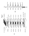
Fig. 1 is an approximate structural view of asemiconductor memory device 1 related to one embodiment of the present invention. -
Fig. 2 is a diagram which shows an approximate structure of onememory string 10 of thesemiconductor memory device 1 related to one embodiment of the present invention. -
Fig. 3 is a diagram which shows a manufacturing process of thesemiconductor memory device 1 related to one embodiment of the present invention. -
Fig. 4 is a diagram which shows a manufacturing process of thesemiconductor memory device 1 related to one embodiment of the present invention. -
Fig. 5 is a diagram which shows a manufacturing process of thesemiconductor memory device 1 related to one embodiment of the present invention. -
Fig. 6 is a diagram which shows a manufacturing process of thesemiconductor memory device 1 related to one embodiment of the present invention. -
Fig. 7 is a diagram which shows a manufacturing process of thesemiconductor memory device 1 related to one embodiment of the present invention. -
Fig. 8 is a diagram which shows a manufacturing process of thesemiconductor memory device 1 related to one embodiment of the present invention. -
Fig. 9 is a diagram which shows a manufacturing process of thesemiconductor memory device 1 related to one embodiment of the present invention. -
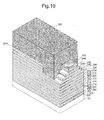
Fig. 10 is a diagram which shows a manufacturing process of thesemiconductor memory device 1 related to one embodiment of the present invention. -
Fig. 11 is a diagram which shows a manufacturing process of thesemiconductor memory device 1 related to one embodiment of the present invention. -
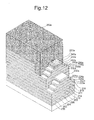
Fig. 12 is a diagram which shows a manufacturing process of thesemiconductor memory device 1 related to one embodiment of the present invention. -
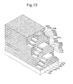
Fig. 13 is a diagram which shows a manufacturing process of thesemiconductor memory device 1 related to one embodiment of the present invention. -
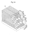
Fig. 14 is a diagram which shows a manufacturing process of thesemiconductor memory device 1 related to one embodiment of the present invention. -
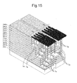
Fig. 15 is a diagram which shows a manufacturing process of thesemiconductor memory device 1 related to one embodiment of the present invention. -
Fig. 16 is an approximate structural view of thesemiconductor memory device 1 related to one embodiment of the present invention. -
Fig. 17 is an approximate structural view of thesemiconductor memory device 1 related to one embodiment of the present invention. -
- 1: semiconductor memory device
- 2: memory transistor region
- 3: word line drive circuit
- 4: source side selection gate line (SGS) drive circuit
- 5: drain side selection gate fine (SGS) drive circuit
- 7: word line (WL)
- 7a: first word line lead line
- 7b: second word line lead line
- 7c: third word line lead line
- 8: bit line (BL)
- 10: memory strings
- 11: column shaped semiconductor
- The semiconductor memory device and manufacturing method of the same related to the embodiments of the present invention are explained below. However, the present invention is not limited to these embodiments. In addition, the same structural elements in each embodiment have the same symbols and in some cases are not explained again.
- An approximate structural view of a
semiconductor memory device 1 of the present invention related to embodiment one is shown inFig. 1 . In the present embodiment, among thesemiconductor memory devices 1 of the present invention a NAND type nonvolatile semiconductor memory device will be explained as an example. Thesemiconductor memory device 1 related to embodiment one includes amemory transistor region 2, a wordline driving circuit 3, a source side selection gate line (SGS)driving circuit 4, a drain side selection gate line (SGD)driving circuit 5, a word line (WL) 7, a word line lead line (first wordline lead line 7a, second wordline lead line 7b and third wordline lead line 7c in the present embodiment), a bit line (BL) 8, a source side selection gate line (SGS) 30 and a drain side selection gate line (SGD) 31 etc. As is shown inFig. 1 , in thesemiconductor memory device 1 of the present invention related to the present embodiment, memory transistors which form thememory transistor region 2 are formed in one series of processes by stacking a plurality of semiconductor layers. In addition, as is shown inFig. 1 , the word line (WL) 7 extends in two directions in each layer and is formed by the same conducting layer in each layer. Thememory transistor region 2 includes a plurality ofmemory strings 10 formed in the shape of a matrix. The bit line (BL) 8 is connected to a sense amplifier 6 (not shown in the figure) and the drain side selection gate line (SGD) 31 is connected to the drain side selection gate lineSGD driving circuit 5 using via holes which are formed at the same time by a photo etching process. - In the
semiconductor memory device 1 of the present invention related to the present embodiment, the end parts of each word line of thememory transistor region 2 are formed in steps. In other words, the width in an approximately parallel direction (approximately perpendicular direction to the second word line lead line direction) with a bit line of the end of theword line 7 which is positioned further upwards is smaller than the width in a bit line direction of theword line 7 which is positioned further downwards. - That is, in the present embodiment, because there are four word lines 7 (four layers, four lines) the following relationship is established for WL1 to WL4 from the lowest word line 7:
width in a direction approximately parallel with a bit line of the end of WL1 > width in a direction approximately parallel with a bit line of the end of WL2 > width in a direction approximately parallel with a bit line of the end of WL3> width in a direction approximately parallel with a bit line of the end of WL4 .....(1). - In addition, in the case where there are n word lines, the following relationship is established:
- width in a direction approximately parallel with a bit line of the end of (k - 1)th word line > width in a direction approximately parallel with a bit line of the end of kth word line.....(2) (k is an integer equal to or larger than 2 and equal to or lower than n).
- Then, the first word line lead line is connected respectively to the end of each word line formed in this step shape. In this way, by forming the end part of each
word line 7 in a step shape it is possible to densely arrange the lead lines of theword line 7. Furthermore, in the present embodiment, an example in which there are four word lines is explained. However, thesemiconductor memory device 1 of the present invention is not limited to four. It is possible to suitably change the number of word lines according to the desired memory capacity and chip area. - The
memory transistor region 2 of thesemiconductor memory device 1 of the present invention related to the present embodiment includes m x n (m, n are both integers) memory strings 10 which are formed in the shape of a matrix. The present embodiment is explained in the case when thememory transistor region 2 includes 8 x 8 memory strings. An approximate structure of one memory string 10 (here, the mnth memory string) of thesemiconductor memory device 1 of the present invention related to the present embodiment is shown inFig. 2 (A) and its equivalent circuit diagram is shown inFig. 2 (B) . The memory strings 10 include four memory transistors MTr1mn to MTr4mn and two selection transistors SSTrmn and SDTrmn, each connected in series respectively. In one of the memory strings 10, a column shapedsemiconductor 11 is formed in anN+ region 15 which is formed in a P type region (P-Well region) 14 on a semiconductor substrate, and aninsulation film 12 is formed around thesemiconductor 11 and flat shaped (planar shaped)electrodes 13a - 13f are formed around theinsulation film 12. Theelectrodes 13a - 13f, theinsulation film 12 and the column shapedsemiconductor 11 form the memory transistors MTr1mn - MTr4mn, the selection transistor SSTrmn and the selection transistor SDTrmn. A silicon oxide film, for example, can be used for theinsulation film 12 of the selection transistor SSTrmn and the selection transistor SDTrmn. In addition, theinsulation film 12 of the memory transistors MTr1mn - MTr4mn include a charge accumulation layer, for example, stacked films of a silicon oxide film, silicon nitride film, and silicon oxide film. Theelectrodes 13b - 13e each become the word lines WL1 - WL4 (7), theelectrode 13f becomes the drain side selection gate line SGDn and theelectrode 13a becomes the source side selection gate line SGS. In addition, abit line BLm 8 is connected to one end of the source/drain of the selection transistor SDTrmn and a source line SL (N+ region 15 in the present embodiment) is connected to the source/drain of the selection transistor SSTrmn. Furthermore, in the present embodiment, an example in which four memory transistors MTr of one memory string 10 (an example of four word lines 7) are connected in series is shown. However, it is not limited to four. The number of memory transistors MTr which form onememory string 10 may be decided according to capacity. - In the present embodiment, each of the memory strings 10 includes a column shaped semiconductor on an n+ region (not shown in the figure) which is formed in the P-
well region 14 of the semiconductor substrate. Each of the memory strings 10 is arranged in a matrix shape on a perpendicular in-plane surface of the column shaped semiconductor. Further, this column shaped semiconductor may have a cylindrical shape or a prism shape. In addition, the column shaped semiconductor refers not only to a symmetrical structure about a center line but also to a column shaped semiconductor which has a step structure in which column shaped semiconductors having a different center line are stacked above the column shaped semiconductor which has symmetry either side of the center line. - In addition, as stated above, because each word line WL1 - WL4 (7) is formed by a common conducting layer in each layer (memory cell layer) in which a plurality of memory cells are formed in two dimensions (that is, in a plane direction) it is possible to significantly reduce the number of word
line driving circuits 3 and realize a reduction in the area of the chip. In addition, the ends of eachword line 7 of thememory transistor region 2 are formed in a step shape and first word line lead lines are respectively connected to the ends of each word line which is formed in this step shape. In this way, by forming the ends of eachword line 7 in a step shape it is possible to densely arrange the lead lines of the word lines 7. - A manufacturing method of the
semiconductor memory device 1 of the present invention related to embodiment one is explained below usingFig. 3 to Fig. 9 . Furthermore, the manufacturing method explained below is one example of a manufacturing method of thesemiconductor memory device 1 of the present invention related to the present embodiment and is not limited to this example. Furthermore, inFig. 3 to Fig. 9 , thememory transistor region 2 and the wordline lead lines 7a - 7c of thesemiconductor memory device 1 related to embodiment one are shown for the purposes of explanation. In addition, in thesemiconductor memory device 1 of the present invention related to embodiment one, an example is explained where there are four word lines 7 (four layers of an amorphous silicon film which form the word lines 7). Furthermore, the number ofword lines 7 is not limited to this. - First, the manufacturing process of peripheral circuit transistors and source side selection gate 30 (lower selection transistor) will be explained. Furthermore, in
Fig.3 to Fig. 9 of the present embodiment, for the purposes of explanation the parts below the sourceside selection gate 30 are collectively shown as thesubstrate part 100 and each structural element is not illustrated. An element separation region (STI) 102 is formed above a semiconductor substrate 101. Next, boron (B) ions are implanted and a P - well region 104 is formed. Further, boron (B) ions are implanted near the surface of the semiconductor substrate 101 and a channel implant region 106 which adjusts the threshold value Vth of a transistor is formed. Here, an N channel type transistor is shown as the transistor which is formed in the peripheral circuit region, however, by implanting ions which create the N type in a desired region, an N-well region is formed and a P channel type transistor is formed. Next, ion impurities such as phosphorus (P) are implanted only in thememory transistor region 2 and an n+ diffusion region 107 which becomes a source line SL is formed. Next, a silicon nitride film and a silicon oxide film are deposited, a photoresist is formed to a desired pattern and a silicon nitride film and silicon oxide film are formed only in thememory transistor region 2 by wet etching. Next, a thick film gate insulation film of a high voltage transistor of the peripheral circuit region is formed, a pattern is formed by the photoresist so that the regions apart from thememory transistor region 2 and the high voltage transistor region are opened, and a thick film gate insulation film is formed by wet etching. A thin film gate insulation film of a high speed operation transistor is formed in the region which is wet etched. Next, after a polysilicon (poly-Si) film and a silicon nitride film which are added with conductive type impurities such as phosphorous (P) are deposited, etching is performed and a gate electrode 110a and a cap silicon nitride film 113a of a transistor in the peripheral circuit region are formed, and a gate electrode 110b and a cap silicon nitride film 113b of a selection transistor in the memory cell region are formed. Next, ions such as P ions or As ions are implanted in the region of the N channel type transistor of the peripheral circuit region and an N type region 112 is formed. Next, the silicon nitride film which is deposited on the entire surface of the substrate is etched by anisotropic etching and a side wall 114 is formed. Next, arsenic (As) ions are implanted in the region of an N channel type transistor of the peripheral circuit region and a source/drain region 116 is formed. Next, B ions are implanted in a P channel type transistor of the peripheral circuit region and a source/drain region is formed. Next, a silicon nitride film (barrier silicon nitride film) 118 is formed on the entire surface of the substrate. Next, an interlayer insulation film (BPSG film) 124 is formed on the entire surface of the substrate and a planarization process is performed by CMP for example. - Next, a photoresist layer is formed and a hole 126 for forming a selection transistor in the shape of a matrix is formed in the
memory transistor region 2. This hole 126 is only formed for the number of memory strings (8 x 8 = 64 in the present embodiment) in thememory transistor region 2. Next, after implanting P ions etc only in thememory transistor region 2, a silicon oxide film and an amorphous silicon film are formed only on a side wall and bottom part of a hole by a method such LPCVD. Next, the silicon oxide film and amorphous silicon film at the bottom part of the hole are etched by RIE and amorphous silicon films 128a to 128d are formed. Next, after forming the amorphous silicon films, a planarization process is performed by CMP for example, and an amorphous silicon film 130 is formed. Next, P ions etc are implanted only in the channel region of the memory transistor. Next, As ions etc are implanted only in thememory transistor region 2 and after forming a drain diffusion layer the As ions are activated by RTA. Then, the peripheral circuit transistor and the lower part selection transistor are complete. Here, P ions are implanted into the channel part. However, ions do not have to be implanted. Next, a silicon nitride film 132 and a silicon oxide film 134 are formed in order on the entire surface of the substrate. Thesubstrate part 100 is completed by the processes up to this point in the present embodiment. The structure and manufacturing process of thesubstrate part 100 are not limited to the examples stated above. - Next, as is shown in
Fig. 3 , anamorphous silicon film 136, asilicon oxide film 138, anamorphous silicon film 140, asilicon oxide film 142, anamorphous silicon film 144, asilicon oxide film 146, an amorphous silicon film 148, asilicon oxide film 150, and asilicon nitride film 152 are formed in order on the entire surface of the substrate. Theamorphous silicon films amorphous silicon films silicon oxide films silicon nitride film 152 is formed to a thickness of 200nm by a CVD method. In addition, theamorphous silicon films - Next, a photoresist 154 (not shown in the figure) is formed on the
silicon nitride film 152, thesilicon nitride film 152 is patterned by a RIE process (Reactive Ion Etching) and asilicon nitride film 152a is formed (Fig. 4 ). Next, a region in which thissilicon nitride film 152 is removed becomes the end region of aword line 7 for connecting a first word line lead line. Next, aBPSG film 156 is formed at a thickness of 600nm for example, on the entire surface of the substrate and a CMP process is performed until the surface of thesilicon nitride film 152 is exposed (Fig. 4 ). - Next, a
photoresist 158 is formed on one part of thesilicon nitride film 152a and one part of theBPSG film 156 as shown inFig. 5 . Thephotoresist 158 andsilicon nitride film 152a are used as a mask, aBPSG film 156, asilicon oxide film 150 and amorphous silicon film 148 are etched using thesilicon oxide film 146 as an etching stopper, and aBPSG film 156a,silicon oxide film 150a andamorphous silicon film 148a are formed. At this time, after theBPSG film 156, asilicon oxide film 150 and amorphous silicon film 148 are etched, a peeling and removing process of thephotoresist 158 is not performed. The width removed from theBPSG film 156,silicon oxide film 150 and amorphous silicon film 148 becomes the width which is exposed of the lowestsilicon oxide film 138. Furthermore, in the present embodiment, an example of etching stacked films is explained using a silicon oxide film as an etching stopper. However, the stacked films may also be etched using an amorphous silicon film as an etching stopper. - Next, the remaining
photoresist 158 is slimmed and thephotoresist 158a is formed as shown inFig. 6 . Then, thephotoresist 158a and thesilicon nitride film 152a are used as a mask, theBPSG film 156a,silicon oxide film 150a,amorphous silicon film 148a,silicon oxide film 146 andamorphous silicon film 144 are etched and the BPSG film 156b, silicon oxide film 150b, amorphous silicon film 148b, silicon oxide film 146a and amorphous silicon film 144a are formed (none of the these films are shown in the figure). In thesemiconductor memory device 1 of the present invention related to the present embodiment, it is possible to form the ends parts of theamorphous silicon films - More specifically, the
photoresist 158a is slimmed again and the photoresist 158b (not shown in the figure) is formed. Then, the photoresist 158b and thesilicon nitride film 152a are used as a mask, the BPSG film 156b, silicon oxide film 150b, amorphous silicon film 148b, silicon oxide film 146a, amorphous silicon film 144a,silicon oxide film 142 andamorphous silicon film 140 are etched, and aBPSG film 156c,silicon oxide film 150c, amorphous silicon film 148c, silicon oxide film 146b,amorphous silicon film 144b,silicon oxide film 142a andamorphous silicon film 140a are formed (Fig. 7 ). Then, the photoresist 158b is removed. - In this way, it is possible to form the end parts of the
amorphous silicon films - Next, a photoresist (not shown in the figure) is formed and a
slit 160 is formed using etching to remove a part of theBPSG film 156c,silicon oxide film 150c, amorphous silicon film 148c, silicon oxide film 146b,amorphous silicon film 144b,silicon oxide film 142a,amorphous silicon film 140a,silicon oxide film 138 and amorphous silicon film 136 (Fig. 8 ). - Next, a hole 170 (not shown in the figure, referred to below as memory plug hole) for forming the column shaped part of a memory cell into the shape of a matrix to match the hole 126 (not shown in the figure) of the
memory transistor region 2. This memory plug hole is formed only for the number of memory strings of the memory transistor region. - Next, a silicon oxide film, silicon nitride film, silicon oxide film and amorphous silicon film (all not shown in the figure) are formed in this order. Next, the amorphous silicon film is etched using RIE and a spacer is formed. The silicon oxide film (first insulation film), silicon nitride film and silicon oxide film (second insulation film) form what is called an ONO film. The silicon nitride film becomes a charge accumulation layer of a memory transistor. Further, an insulation film such as an alumina film may be used instead of the silicon oxide film.
- Next, a silicon oxide film, silicon nitride film and silicon oxide film are etched using the spacer of the amorphous silicon film which is formed in the memory plug hole 170, and a part of the amorphous silicon film 130 which is formed in the hole 126 is exposed. Next, after forming an amorphous silicon film so that the memory plug hole 170 is filled, a planarization process is performed by CMP for example. Next, As ions are implanted, an RTA process is performed and a drain diffusion layer 172 is formed. Then, an upper part selection transistor is formed by a process similar to the process for forming a lower part selection transistor.
- Next, as is shown in
Fig. 9 , a contact hole is formed up to the amorphous silicon film 148c,amorphous silicon film 144b,amorphous silicon film 140a, andamorphous silicon film 136 respectively, and first wordline lead lines 7a which are connected to the amorphous silicon film 148c,amorphous silicon film 144b,amorphous silicon film 140a, andamorphous silicon film 136 respectively are formed. Third wordline lead lines 7c may be formed at the same time as the process for forming the first wordline lead lines 7a. Then, wires such as a bit line and first word line lead lines are formed and thesemiconductor memory device 1 of the present invention related to the present embodiment is complete. - In the
semiconductor memory device 1 of the present invention related to the present embodiment, because each word line WL1 - WL4 (7) is formed by a common conducting layer for each layer (memory cell layer) in which a plurality of memory cells are formed in two dimensions (that is, in a planar direction), it is possible to significantly reduce the number of wordline driving circuits 3 and realize a reduction in chip size. In addition, the end part of eachword line 7 of thememory transistor region 2 is formed in a step shape and first wordline lead lines 7a are respectively connected to the end part of each word line formed in this step shape. In this way, it is possible to densely arrange lead lines of theword line 7 by forming the end part of eachword line 7 in a step shape. - In the
semiconductor memory device 1 of the present invention related to embodiment one, an example is explained in which the ends ofword lines 7 were each formed in step shapes in a direction parallel withbit lines 8. In thesemiconductor memory device 1 of the present invention related to embodiment two, the step shaped structure of the ends ofword lines 7 as in embodiment one is formed in a direction parallel to abit line 8 and a plurality of these step shaped structures are formed in a perpendicular direction to thebit line 8. As a result, it is possible to more densely form the word line lead lines. Furthermore, because thesemiconductor memory device 1 related to embodiment two has the same structure as thesemiconductor memory device 1 related to embodiment one apart from the structure of the end parts of theword lines 7, the structure which is the same as thesemiconductor memory device 1 related to embodiment one will not be explained again here. - A manufacturing method of the
semiconductor memory device 1 of the present invention related to embodiment two will be explained usingFig. 10 - Fig. 15 . Furthermore, the manufacturing method explained below is one example of a manufacturing method of thesemiconductor memory device 1 of the present invention related to the present embodiment and is not limited to this example. In addition, for the purposes of explanation, thememory transistor region 2 and the wordline lead lines 7a - 7c of the semiconductor memory device related to embodiment two are shown inFig. 10 to Fig. 15 . In thesemiconductor memory device 1 of the present invention related to embodiment two, an example is explained in the case where there are twelve word lines 7 (twelve amorphous silicon layers which form the word lines 7). Further, the number ofword lines 7 is not limited to this number. - First, a
substrate part 100 is formed by the same method explained in embodiment one. Then, anamorphous silicon film 200, asilicon oxide film 202, anamorphous silicon film 204, asilicon oxide film 206, anamorphous silicon film 208, asilicon oxide film 210, anamorphous silicon film 212, asilicon oxide film 214, anamorphous silicon film 216, asilicon oxide film 218, anamorphous silicon film 220, asilicon oxide film 222, anamorphous silicon film 224, asilicon oxide film 226, anamorphous silicon film 228, asilicon oxide film 230, anamorphous silicon film 232, asilicon oxide film 234, anamorphous silicon film 236, asilicon oxide film 238, anamorphous silicon film 240, asilicon oxide film 242, anamorphous silicon film 244, asilicon oxide film 246 and asilicon nitride film 248 are formed in order on thesubstrate part 100. Next, a part of thesilicon nitride film 248 is etched, aBPSG film 250 is formed and a CMP process is performed until the surface of thesilicon nitride film 248 is exposed. Then, aphotoresist 252 is formed and theamorphous silicon film 236,silicon oxide film 238,amorphous silicon film 240,silicon oxide film 242,amorphous silicon film 244,silicon oxide film 246 andBPGS film 250 are formed in a step shape using the same process explained in embodiment one (Fig. 10 ). - Next, the
amorphous silicon film 232,silicon oxide film 234,amorphous silicon film 236,silicon oxide film 238,amorphous silicon film 240,silicon oxide film 242,amorphous silicon film 244,silicon oxide film 246 andBPSG film 250, andamorphous silicon film 220,silicon oxide film 222,amorphous silicon film 224,silicon oxide film 226,amorphous silicon film 228 andsilicon oxide film 230 are etched together using thephotoresist 252, and theamorphous silicon film 232a,silicon oxide film 234a,amorphous silicon film 236a,silicon oxide film 238a,amorphous silicon film 240a,silicon oxide film 242a,amorphous silicon film 244a,silicon oxide film 246a andBPSG film 250a, and theamorphous silicon film 220a,silicon oxide film 222a,amorphous silicon film 224a,silicon oxide film 226a,amorphous silicon film 228a andsilicon oxide film 230a are formed (Fig. 11 ). - Then, the
photoresist 252 is slimmed without peeling and aphotoresist 252a is formed (Fig. 12 ). Next, theamorphous silicon film 232a,silicon oxide film 234a,amorphous silicon film 236a,silicon oxide film 238a,amorphous silicon film 240a,silicon oxide film 242a,amorphous silicon film 244a,silicon oxide film 246a andBPSG film 250a and theamorphous silicon film 220a,silicon oxide film 222a,amorphous silicon film 224a,silicon oxide film 226a,amorphous silicon film 228a andsilicon oxide film 230a and theamorphous silicon film 204,silicon oxide film 206,amorphous silicon film 208,silicon oxide film 210,amorphous silicon film 212 andsilicon oxide film 214,amorphous silicon film 216 andsilicon oxide film 218 are etched together and theamorphous silicon film 232b,silicon oxide film 234b,amorphous silicon film 236b,silicon oxide film 238b,amorphous silicon film 240b,silicon oxide film 242b,amorphous silicon film 244b,silicon oxide film 246b andBPSG film 250b and theamorphous silicon film 220b,silicon oxide film 222b,amorphous silicon film 224b,silicon oxide film 226b,amorphous silicon film 228b andsilicon oxide film 230b and theamorphous silicon film 204a,silicon oxide film 206a,amorphous silicon film 208a,silicon oxide film 210a,amorphous silicon film 212a,silicon oxide film 214a, amorphous silicon film 216a and silicon oxide film 218a are formed (Fig. 13 ). - Following this, the
photoresist 252a is removed by peeling. Next, a photoresist (not shown in the figure) is formed and aslit 260 is formed the same as in embodiment one (Fig. 14 ). - Next, memory plug holes 170 (not shown in the figure) are formed only for the number of memory strings by the same process as in embodiment one. Next, a silicon oxide film, silicon nitride film, silicon oxide film and amorphous silicon film (all not shown in the figure) are formed in this order. Next, the amorphous silicon film is etched by RIE and a spacer is formed. The silicon oxide film (first insulation film), silicon nitride film and silicon oxide film (second insulation film) form what is called an ONO film. The silicon nitride film becomes a charge accumulation layer of the memory transistor. Furthermore, an insulation film such as alumina may be used instead of the silicon oxide film.
- Next, the silicon oxide film, silicon nitride film and silicon oxide film are etched using the spacer of the amorphous silicon film formed in the memory plug hole 170 and a part of the amorphous silicon film 130 formed in the hole 126 is exposed. Next, after forming an amorphous silicon film in order to fill the memory plug hole 170 a planarization process is performed by CMP for example. Next, As ions are implanted and a drain diffusion layer 172 is formed using RTA. Then, an upper part selection transistor is formed by the same process which forms the lower part selection transistor.
- Next, as is shown in
Fig. 15 , theamorphous silicon films lines 7a which connect to theamorphous silicon films line lead lines 7c may be formed at the same time as the process for forming the first wordline lead lines 7a. Then, bit line wires and first word line lead line wires are formed and thesemiconductor memory device 1 of the present invention related to the present embodiment is complete. - In the
semiconductor memory device 1 of the present invention related to embodiment two, the step shaped structure of the end part of theword lines 7 as in embodiment one is formed in a direction parallel to abit line 8, and a plurality of these step shaped structures are also formed in a direction perpendicular to abit line 8. As a result, it is possible to more densely form the word line lead lines. - The
semiconductor memory device 1 of the present invention related to embodiment three includes a structure in which a plurality ofsemiconductor memory devices 1 related to embodiment one are stacked in a longitudinal direction. Furthermore, because other structures are the same as in thesemiconductor memory device 1 of the present invention related to embodiment one, they will not be explained again here. - As is shown in
Fig. 16 , thesemiconductor memory device 1 of the present invention related to embodiment three has a structure in which threesemiconductor memory devices 1 of the present invention related to embodiment one are stacked in a longitudinal direction. Furthermore, in embodiment three, threesemiconductor memory devices 1 of the present invention related to embodiment one which are stacked in a longitudinal direction are explained as an example. However, the number is not limited to three. - According to the
semiconductor memory device 1 of the present invention related to embodiment three it is possible to more densely integrate memory transistors. - The
semiconductor memory device 1 of the present invention related to embodiment four includes a structure in which a plurality ofsemiconductor memory devices 1 of the present invention related to embodiment two are stacked in a longitudinal direction. Furthermore, because other structures are the same as in thesemiconductor memory device 1 of the present invention related to embodiment two, they will not be explained again here. - As is shown in
Fig. 17 , thesemiconductor memory device 1 of the present invention related to embodiment four has a structure in which twosemiconductor memory devices 1 of the present invention related to embodiment two are stacked in a longitudinal direction. Furthermore, in embodiment four, twosemiconductor memory devices 1 of the present invention related to embodiment two which are stacked in a longitudinal direction are explained as an example. However, the number is not limited to two. - According to the
semiconductor memory device 1 of the present invention related to embodiment four it is possible to more densely integrate memory transistors.
Claims (20)
- A semiconductor memory device comprising:a plurality of memory strings having a plurality of electrically reprogrammable memory cells connected in series, the memory strings having a column shaped semiconductor, a first insulation film formed around the column shaped semiconductor, a charge accumulation layer formed around the first insulation film, a second insulation film formed around the charge accumulation layer and a plurality of electrodes formed around the second insulation film;a plurality of bit lines respectively connected to one end of the plurality of memory strings via a plurality of selection transistors; anda plurality of conducting layers formed by the plurality of electrodes of the plurality of memory strings, the plurality of electrodes of the plurality of memory strings being shared with the plurality of electrodes of different memory strings, the plurality of conducting layers extending in two dimensions respectively, and each end part of the plurality of conducting layers being formed in step shapes in a direction parallel with the plurality of bit lines.
- The semiconductor memory device according to claim 1, wherein an end part of the plurality of conducting layers is also formed in step shapes in a direction perpendicular to the plurality of bit lines.
- The semiconductor memory device according to claim 1, wherein both ends of the plurality of conducting layers in the direction of the plurality of bit lines have step shapes.
- The semiconductor memory device according to claim 1, wherein a plurality of word lead lines are each arranged on the ends of the plurality of conducting layers formed in step shapes.
- The semiconductor memory device according to claim 1, wherein a plurality of contacts is each arranged on the ends of the plurality of conducting layers formed in step shapes.
- The semiconductor memory device according to claim 1, wherein the plurality of conducting layers which extend in two dimensions are each plate shaped.
- The semiconductor memory device according to claim 1, wherein the plurality of memory strings are arranged in a matrix in an in-plane surface perpendicular to the column shaped semiconductor.
- A semiconductor memory device comprising:a substrate:a plurality of memory strings having a plurality of electrically reprogrammable memory cells connected in series, the plurality of memory strings having a column shaped semiconductor, a first insulation film formed around the column shaped semiconductor, a charge accumulation layer formed around the first insulation film, a second insulation film formed around the charge accumulation film and a plurality of electrodes formed around the second insulation film;a plurality of bit lines respectively connected to one end of the plurality of memory strings via a plurality of selection transistors; anda plurality of conducting layers formed by the plurality of electrodes of the plurality of memory strings, the plurality of electrodes of the plurality of memory strings being shared with the plurality of electrodes of different memory strings, the plurality of conducting layers extending in two dimensions respectively on the substrate, and each end part of the plurality of conducting layers being formed in step shapes in a direction parallel with the plurality of bit lines, and the widths of the end part of the plurality of conducting layers each meet the following formula when the plurality of conducting layers of the substrate side is a first conducting layer;width of the end of (k - 1)th conducting layer > width of the end of kth conducting layer (k is an integer equal to or larger than 2).
- The semiconductor memory device according to claim 8, wherein an end part of the plurality of conducting layers is also formed in step shapes in a direction perpendicular to the plurality of bit lines.
- The semiconductor memory device according to claim 8, wherein both ends of the plurality of conducting layers in the direction of the plurality of bit lines have step shapes.
- The semiconductor memory device according to claim 8, wherein a plurality of word lead lines are each arranged on the ends of the plurality of conducting layers formed in step shapes.
- The semiconductor memory device according to claim 8, wherein a plurality of contacts are each arranged on the ends of the plurality of conducting layers formed in step shapes.
- The semiconductor memory device according to claim 8, wherein the plurality of memory strings are arranged in a matrix in an in-plane surface perpendicular to the column shaped semiconductor.
- A method of manufacturing a semiconductor device comprising:forming a diffusion region of conducting impurities on a semiconductor substrate;forming a plurality of alternating insulation films and a plurality of conductors above the semiconductor substrate;forming a first protective film in a memory region and a second protective film in an end part region on the uppermost conducting layer;forming a plurality of holes in the plurality of alternating insulation films and conductors of the memory region;forming a second insulation film on a surface of the plurality of holes;etching the second insulation film at the bottom part of the plurality of holes;forming a column shaped semiconductor in the plurality of holes;forming a photoresist on the second insulation film;removing the conductor of the end part region;slimming the photoresist film; andforming the end part of the conductors in step shapes by further removing the conductor of the end part region after slimming.
- The method of manufacturing a semiconductor device according to claim 14, wherein the end part of the conductors are formed in step shapes by repeating slimming and etching.
- The method of manufacturing a semiconductor device according to claim 14, wherein the end part of the plurality of conducting layers is further formed in step shapes in a direction perpendicular to the plurality of bit lines.
- The method of manufacturing a semiconductor device according to claim 14, wherein both ends of the plurality of conducting layers in the plurality of bit lines direction have step shapes.
- The method of manufacturing a semiconductor device according to claim 14, wherein a plurality of word lead lines are each arranged on the ends of the plurality of conducting layers formed in step shapes.
- The method of manufacturing a semiconductor device according to claim 14, wherein a plurality of contacts are each arranged on the ends of the plurality of conducting layers formed in step shapes.
- The method of manufacturing a semiconductor device according to claim 14, wherein the plurality of memory strings are arranged in a matrix in an in-plane surface perpendicular to the column shaped semiconductor.
Applications Claiming Priority (2)
| Application Number | Priority Date | Filing Date | Title |
|---|---|---|---|
| JP2007100086A JP5091526B2 (en) | 2007-04-06 | 2007-04-06 | Semiconductor memory device and manufacturing method thereof |
| PCT/JP2008/056714 WO2008126774A1 (en) | 2007-04-06 | 2008-04-03 | Semiconductor memory device and method for manufacturing the same |
Publications (2)
| Publication Number | Publication Date |
|---|---|
| EP2136398A1 true EP2136398A1 (en) | 2009-12-23 |
| EP2136398A4 EP2136398A4 (en) | 2011-04-20 |
Family
ID=39863874
Family Applications (1)
| Application Number | Title | Priority Date | Filing Date |
|---|---|---|---|
| EP08739821A Withdrawn EP2136398A4 (en) | 2007-04-06 | 2008-04-03 | SEMICONDUCTOR MEMORY COMPONENT AND METHOD FOR MANUFACTURING THE SAME |
Country Status (7)
| Country | Link |
|---|---|
| US (2) | US8659070B2 (en) |
| EP (1) | EP2136398A4 (en) |
| JP (1) | JP5091526B2 (en) |
| KR (1) | KR101126834B1 (en) |
| CN (2) | CN101647114A (en) |
| TW (1) | TW200903738A (en) |
| WO (1) | WO2008126774A1 (en) |
Cited By (7)
| Publication number | Priority date | Publication date | Assignee | Title |
|---|---|---|---|---|
| US8822971B2 (en) | 2011-11-25 | 2014-09-02 | Samsung Electronics Co., Ltd. | Semiconductor memory device having three-dimensionally arranged resistive memory cells |
| JP2014183225A (en) * | 2013-03-19 | 2014-09-29 | Toshiba Corp | Nonvolatile semiconductor storage device |
| JP2014195034A (en) * | 2013-03-29 | 2014-10-09 | Macronix International Co Ltd | Three-dimensional nand flash memory |
| EP2715787A4 (en) * | 2011-06-02 | 2014-10-29 | Micron Technology Inc | APPARATUSES INCLUDING STAIRCASE STRUCTURES AND METHODS OF MAKING SAME |
| WO2016028484A1 (en) * | 2014-08-19 | 2016-02-25 | Sandisk 3D Llc | Word line connection for memory device and method of making thereof |
| EP3306664A1 (en) * | 2016-10-10 | 2018-04-11 | Macronix International Co., Ltd. | Interlevel connectors in multilevel circuitry, and method for forming the same |
| EP4521879A3 (en) * | 2019-01-31 | 2025-06-04 | Yangtze Memory Technologies Co., Ltd. | Staircase formation in three-dimensional memory device |
Families Citing this family (102)
| Publication number | Priority date | Publication date | Assignee | Title |
|---|---|---|---|---|
| JP5091526B2 (en) * | 2007-04-06 | 2012-12-05 | 株式会社東芝 | Semiconductor memory device and manufacturing method thereof |
| JP4691124B2 (en) | 2008-03-14 | 2011-06-01 | 株式会社東芝 | Method for manufacturing nonvolatile semiconductor memory device |
| KR101434588B1 (en) | 2008-06-11 | 2014-08-29 | 삼성전자주식회사 | Semiconductor device and manufacturing method thereof |
| JP5086959B2 (en) * | 2008-09-26 | 2012-11-28 | 株式会社東芝 | Nonvolatile semiconductor memory device |
| JP5364336B2 (en) * | 2008-11-04 | 2013-12-11 | 株式会社東芝 | Semiconductor memory device |
| JP5300419B2 (en) * | 2008-11-05 | 2013-09-25 | 株式会社東芝 | Nonvolatile semiconductor memory device and manufacturing method thereof |
| JP5330017B2 (en) | 2009-02-17 | 2013-10-30 | 株式会社東芝 | Nonvolatile semiconductor memory device and manufacturing method thereof |
| KR101660944B1 (en) | 2009-07-22 | 2016-09-28 | 삼성전자 주식회사 | Vertical type non-volatile memory device and method of manufacturing the same |
| KR101097465B1 (en) | 2009-07-30 | 2011-12-23 | 주식회사 하이닉스반도체 | Method for forming nonvolatile memory device |
| JP4929332B2 (en) | 2009-09-24 | 2012-05-09 | 株式会社東芝 | Manufacturing method of electronic parts |
| KR20110042619A (en) | 2009-10-19 | 2011-04-27 | 삼성전자주식회사 | 3D semiconductor device and manufacturing method thereof |
| US8158967B2 (en) | 2009-11-23 | 2012-04-17 | Micron Technology, Inc. | Integrated memory arrays |
| US20130009274A1 (en) * | 2009-12-31 | 2013-01-10 | Industry-University Cooperation Foundation Hanyang University | Memory having three-dimensional structure and manufacturing method thereof |
| JP2011142276A (en) | 2010-01-08 | 2011-07-21 | Toshiba Corp | Nonvolatile semiconductor memory device and manufacturing method thereof |
| KR101660488B1 (en) | 2010-01-22 | 2016-09-28 | 삼성전자주식회사 | Three Dimensional Semiconductor Memory Device And Method Of Fabricating The Same |
| TWI798525B (en) * | 2010-02-16 | 2023-04-11 | 凡 歐貝克 | System comprising a semiconductor device and structure |
| KR101702060B1 (en) * | 2010-02-19 | 2017-02-02 | 삼성전자주식회사 | Interconnection structure for three-dimensional semiconductor device |
| KR101102548B1 (en) * | 2010-04-30 | 2012-01-04 | 한양대학교 산학협력단 | Nonvolatile Memory Device and Manufacturing Method Thereof |
| KR101624978B1 (en) | 2010-05-18 | 2016-05-30 | 삼성전자주식회사 | Semiconductor Device and Method of fabricating the same |
| KR101713228B1 (en) * | 2010-06-24 | 2017-03-07 | 삼성전자주식회사 | Semiconductor memory devices having asymmetric wordline pads |
| US8890233B2 (en) * | 2010-07-06 | 2014-11-18 | Macronix International Co., Ltd. | 3D memory array with improved SSL and BL contact layout |
| JP5651415B2 (en) | 2010-09-21 | 2015-01-14 | 株式会社東芝 | Nonvolatile semiconductor memory device and manufacturing method thereof |
| JP5269022B2 (en) * | 2010-09-22 | 2013-08-21 | 株式会社東芝 | Semiconductor memory device |
| US8822287B2 (en) | 2010-12-10 | 2014-09-02 | Samsung Electronics Co., Ltd. | Methods of manufacturing semiconductor devices |
| JP2012174892A (en) * | 2011-02-22 | 2012-09-10 | Toshiba Corp | Semiconductor storage device and manufacturing method of the same |
| JP5330440B2 (en) * | 2011-03-23 | 2013-10-30 | 株式会社東芝 | Manufacturing method of semiconductor device |
| US9741736B2 (en) * | 2011-05-20 | 2017-08-22 | Kabushiki Kaisha Toshiba | Semiconductor memory device |
| JP5550604B2 (en) * | 2011-06-15 | 2014-07-16 | 株式会社東芝 | Three-dimensional semiconductor device and manufacturing method thereof |
| KR101250851B1 (en) * | 2011-06-30 | 2013-04-04 | 서울대학교산학협력단 | Contact process method for 3d stacked memory array |
| KR20130046700A (en) * | 2011-10-28 | 2013-05-08 | 삼성전자주식회사 | Semiconductor memory device including three-dimensionally arranged memory elements |
| US9673389B2 (en) * | 2012-01-24 | 2017-06-06 | Kabushiki Kaisha Toshiba | Memory device |
| CN103258824B (en) * | 2012-02-20 | 2016-02-17 | 中芯国际集成电路制造(上海)有限公司 | The memory cell of flash memory and formation method |
| US8912089B2 (en) | 2012-09-05 | 2014-12-16 | Kabushiki Kaisha Toshiba | Method for manufacturing a semiconductor device including a stacked body comprising pluralities of first and second metallic conductive layers |
| KR20140075340A (en) * | 2012-12-11 | 2014-06-19 | 에스케이하이닉스 주식회사 | Semiconductor device and method of manufacturing the same |
| US9219074B2 (en) * | 2014-01-17 | 2015-12-22 | Macronix International Co., Ltd. | Three-dimensional semiconductor device |
| KR102024723B1 (en) | 2013-01-02 | 2019-09-24 | 삼성전자주식회사 | Three dimensional semiconductor device |
| US9165823B2 (en) * | 2013-01-08 | 2015-10-20 | Macronix International Co., Ltd. | 3D stacking semiconductor device and manufacturing method thereof |
| KR102046504B1 (en) * | 2013-01-17 | 2019-11-19 | 삼성전자주식회사 | Step shape pad structure and wiring structure in vertical type semiconductor device |
| KR102045249B1 (en) * | 2013-01-18 | 2019-11-15 | 삼성전자주식회사 | Wiring structure of 3-dimension semiconductor device |
| US9111591B2 (en) | 2013-02-22 | 2015-08-18 | Micron Technology, Inc. | Interconnections for 3D memory |
| KR102028086B1 (en) | 2013-03-04 | 2019-10-04 | 삼성전자주식회사 | Memory device and apparatus including the same |
| US10224279B2 (en) * | 2013-03-15 | 2019-03-05 | Monolithic 3D Inc. | Semiconductor device and structure |
| JP2014192243A (en) * | 2013-03-26 | 2014-10-06 | Toshiba Corp | Semiconductor memory device |
| US9165937B2 (en) * | 2013-07-01 | 2015-10-20 | Micron Technology, Inc. | Semiconductor devices including stair step structures, and related methods |
| JP2015028990A (en) * | 2013-07-30 | 2015-02-12 | 株式会社東芝 | Nonvolatile memory device |
| JP2015056452A (en) | 2013-09-10 | 2015-03-23 | 株式会社東芝 | Semiconductor memory device and manufacturing method thereof |
| KR102190384B1 (en) | 2013-10-14 | 2020-12-14 | 삼성전자주식회사 | Method of fabricating a semiconductor device |
| KR20150056309A (en) | 2013-11-15 | 2015-05-26 | 삼성전자주식회사 | Three-dimensional semiconductor devices and fabricating methods thereof |
| KR20150057147A (en) | 2013-11-18 | 2015-05-28 | 삼성전자주식회사 | Memory device |
| CN104766862A (en) * | 2014-01-06 | 2015-07-08 | 旺宏电子股份有限公司 | Three-dimensional memory structure and its manufacturing method |
| KR102183713B1 (en) | 2014-02-13 | 2020-11-26 | 삼성전자주식회사 | Staircase Connection Structure Of Three-Dimensional Semiconductor Device And Method Of Forming The Same |
| CN103871965B (en) * | 2014-03-19 | 2017-02-08 | 武汉新芯集成电路制造有限公司 | Method for forming stepped contact holes |
| CN104319276B (en) * | 2014-09-16 | 2017-05-10 | 华中科技大学 | Gate electrode for nonvolatile three-dimensional semiconductor memory, and preparation method for gate electrode |
| US9142538B1 (en) * | 2014-09-18 | 2015-09-22 | Macronix International Co., Ltd. | Three-dimensional semiconductor device |
| CN105826296B (en) * | 2015-01-09 | 2018-09-14 | 旺宏电子股份有限公司 | Pad structure |
| KR20160096309A (en) | 2015-02-05 | 2016-08-16 | 에스케이하이닉스 주식회사 | 3-dimension non-volatile semiconductor device |
| KR102649372B1 (en) * | 2016-01-08 | 2024-03-21 | 삼성전자주식회사 | Three dimensional semiconductor memory device |
| US10049744B2 (en) | 2016-01-08 | 2018-08-14 | Samsung Electronics Co., Ltd. | Three-dimensional (3D) semiconductor memory devices and methods of manufacturing the same |
| CN105655368B (en) * | 2016-01-15 | 2018-09-25 | 中国科学院上海微系统与信息技术研究所 | A kind of three-dimensional stacked phase change memory array device and preparation method thereof |
| KR102650535B1 (en) | 2016-01-18 | 2024-03-25 | 삼성전자주식회사 | Three dimensional semiconductor memory device |
| JP6495838B2 (en) * | 2016-01-27 | 2019-04-03 | 東芝メモリ株式会社 | Semiconductor memory device and manufacturing method thereof |
| KR102635843B1 (en) | 2016-02-26 | 2024-02-15 | 삼성전자주식회사 | Semiconductor device |
| KR20170121785A (en) | 2016-04-25 | 2017-11-03 | 삼성전자주식회사 | Three-Dimensional Semiconductor Device |
| US9691786B1 (en) | 2016-04-29 | 2017-06-27 | Kabushiki Kaisha Toshiba | Semiconductor memory device |
| JP2018037513A (en) * | 2016-08-31 | 2018-03-08 | 東芝メモリ株式会社 | Semiconductor device |
| KR102741613B1 (en) * | 2016-12-21 | 2024-12-16 | 삼성전자주식회사 | Three dimensional semiconductor memory device |
| KR102508918B1 (en) | 2016-12-22 | 2023-03-10 | 삼성전자주식회사 | Vertical semiconductor devices |
| KR101799069B1 (en) * | 2017-02-28 | 2017-11-20 | 삼성전자주식회사 | Semiconductor memory devices having asymmetric wordline pads |
| US10991762B2 (en) * | 2017-03-31 | 2021-04-27 | Sony Semiconductor Solutions Corporation | Memory unit |
| KR20250048115A (en) | 2017-06-02 | 2025-04-07 | 가부시키가이샤 한도오따이 에네루기 켄큐쇼 | Semiconductor device, electronic component, and electronic device |
| JP7195068B2 (en) | 2017-06-26 | 2022-12-23 | 株式会社半導体エネルギー研究所 | Semiconductor equipment, electronic equipment |
| US11133336B2 (en) | 2017-06-27 | 2021-09-28 | Semiconductor Energy Laboratory Co., Ltd. | Semiconductor device and manufacturing method of semiconductor device |
| US11374012B2 (en) | 2017-07-06 | 2022-06-28 | Semiconductor Energy Laboratory Co., Ltd. | Semiconductor device and driving method of semiconductor device |
| US10665604B2 (en) | 2017-07-21 | 2020-05-26 | Semiconductor Energy Laboratory Co., Ltd. | Semiconductor device, semiconductor wafer, memory device, and electronic device |
| JP6863864B2 (en) * | 2017-09-08 | 2021-04-21 | キオクシア株式会社 | Storage device |
| KR102403732B1 (en) * | 2017-11-07 | 2022-05-30 | 삼성전자주식회사 | 3D nonvolatile memory device |
| CN107863351B (en) * | 2017-11-21 | 2019-03-19 | 长江存储科技有限责任公司 | A manufacturing method of high-stacked 3D NAND flash memory and 3D NAND flash memory |
| US10147638B1 (en) | 2017-12-29 | 2018-12-04 | Micron Technology, Inc. | Methods of forming staircase structures |
| US10886364B2 (en) * | 2018-02-06 | 2021-01-05 | International Business Machines Corporation | Vertical memory cell with mechanical structural reinforcement |
| JP2019161059A (en) | 2018-03-14 | 2019-09-19 | 東芝メモリ株式会社 | Semiconductor memory device |
| KR102628007B1 (en) | 2018-05-09 | 2024-01-22 | 삼성전자주식회사 | Vertical Memory Device |
| CN109155317B (en) | 2018-05-18 | 2019-11-26 | 长江存储科技有限责任公司 | Step formation in three-dimensional memory devices |
| KR102619626B1 (en) | 2018-06-12 | 2023-12-29 | 삼성전자주식회사 | Three-dimensional semiconductor memory device |
| CN108807410B (en) * | 2018-07-16 | 2021-02-05 | 长江存储科技有限责任公司 | 3D memory device and method of manufacturing the same |
| WO2020029216A1 (en) * | 2018-08-10 | 2020-02-13 | Yangtze Memory Technologies Co., Ltd. | Multi-division 3d nand memory device |
| CN109496354B (en) * | 2018-10-18 | 2020-01-17 | 长江存储科技有限责任公司 | Method for forming a multi-partition ladder structure of a three-dimensional memory device |
| KR102736178B1 (en) | 2019-01-15 | 2024-12-02 | 삼성전자주식회사 | Three dimensional semiconductor memory device and method of fabricating the same |
| JP7132142B2 (en) * | 2019-02-05 | 2022-09-06 | キオクシア株式会社 | Semiconductor memory device manufacturing method |
| US10937801B2 (en) * | 2019-03-22 | 2021-03-02 | Sandisk Technologies Llc | Three-dimensional memory device containing a polygonal lattice of support pillar structures and contact via structures and methods of manufacturing the same |
| AU2019464174B2 (en) * | 2019-08-23 | 2022-06-23 | Yangtze Memory Technologies Co., Ltd. | Vertical memory devices |
| CN110828471B (en) * | 2019-10-25 | 2023-02-07 | 长江存储科技有限责任公司 | 3D memory device and manufacturing method thereof |
| CN111357109B (en) | 2020-02-17 | 2021-06-08 | 长江存储科技有限责任公司 | Multi-partition stepped structure of three-dimensional memory device and forming method thereof |
| KR102687679B1 (en) * | 2020-02-25 | 2024-07-24 | 양쯔 메모리 테크놀로지스 씨오., 엘티디. | 3D NAND memory device and method of forming the same |
| CN111430352A (en) * | 2020-04-08 | 2020-07-17 | 长江存储科技有限责任公司 | A three-dimensional memory and its manufacturing method |
| DE102020123746B4 (en) | 2020-05-29 | 2023-02-16 | Taiwan Semiconductor Manufacturing Co., Ltd. | Three-dimensional non-volatile memory device and method of making same |
| US11640974B2 (en) | 2020-06-30 | 2023-05-02 | Taiwan Semiconductor Manufacturing Co., Ltd. | Memory array isolation structures |
| US11647634B2 (en) | 2020-07-16 | 2023-05-09 | Taiwan Semiconductor Manufacturing Co., Ltd. | Three-dimensional memory device and method |
| US11355516B2 (en) | 2020-07-16 | 2022-06-07 | Taiwan Semiconductor Manufacturing Co., Ltd. | Three-dimensional memory device and method |
| US11423966B2 (en) * | 2020-07-30 | 2022-08-23 | Taiwan Semiconductor Manufacturing Co., Ltd. | Memory array staircase structure |
| JP7562449B2 (en) * | 2021-03-03 | 2024-10-07 | キオクシア株式会社 | Semiconductor memory device and its manufacturing method |
| JP2023098145A (en) | 2021-12-28 | 2023-07-10 | キオクシア株式会社 | semiconductor storage device |
| CN115799216A (en) * | 2022-12-20 | 2023-03-14 | 成都皮兆永存科技有限公司 | Interconnection structure of high-density three-dimensional stacked memory and preparation method |
Family Cites Families (17)
| Publication number | Priority date | Publication date | Assignee | Title |
|---|---|---|---|---|
| JP3229012B2 (en) | 1992-05-21 | 2001-11-12 | 株式会社東芝 | Method for manufacturing semiconductor device |
| JPH0644896A (en) | 1992-07-24 | 1994-02-18 | Mitsubishi Materials Corp | Method of manufacturing electron beam control electrode plate of flat display device |
| JP3651689B2 (en) * | 1993-05-28 | 2005-05-25 | 株式会社東芝 | NAND type nonvolatile semiconductor memory device and manufacturing method thereof |
| US5705885A (en) | 1994-11-25 | 1998-01-06 | Kabushiki Kaisha Toshiba | Brazing structure for X-ray image intensifier |
| KR0165398B1 (en) | 1995-05-26 | 1998-12-15 | 윤종용 | Vertical transistor manufacturing method |
| JP3853406B2 (en) * | 1995-10-27 | 2006-12-06 | エルピーダメモリ株式会社 | Semiconductor integrated circuit device and method for manufacturing the same |
| JP3934867B2 (en) * | 2000-09-29 | 2007-06-20 | 株式会社東芝 | Nonvolatile semiconductor memory device and nonvolatile semiconductor memory system |
| JP3566944B2 (en) * | 2001-06-23 | 2004-09-15 | 富士雄 舛岡 | Semiconductor storage device and method of manufacturing the same |
| KR100483035B1 (en) | 2001-03-30 | 2005-04-15 | 샤프 가부시키가이샤 | A semiconductor memory and its production process |
| JP3963664B2 (en) | 2001-06-22 | 2007-08-22 | 富士雄 舛岡 | Semiconductor memory device and manufacturing method thereof |
| JP2004356207A (en) * | 2003-05-27 | 2004-12-16 | Fujio Masuoka | Semiconductor storage device and method of manufacturing the same |
| JP2006128390A (en) * | 2004-10-28 | 2006-05-18 | Toshiba Corp | Semiconductor device and manufacturing method thereof |
| JP5016832B2 (en) * | 2006-03-27 | 2012-09-05 | 株式会社東芝 | Nonvolatile semiconductor memory device and manufacturing method thereof |
| JP4768557B2 (en) * | 2006-09-15 | 2011-09-07 | 株式会社東芝 | Nonvolatile semiconductor memory device and manufacturing method thereof |
| JP2008160004A (en) | 2006-12-26 | 2008-07-10 | Toshiba Corp | Semiconductor memory device and manufacturing method thereof |
| JP5091491B2 (en) | 2007-01-23 | 2012-12-05 | 株式会社東芝 | Nonvolatile semiconductor memory device |
| JP5091526B2 (en) * | 2007-04-06 | 2012-12-05 | 株式会社東芝 | Semiconductor memory device and manufacturing method thereof |
-
2007
- 2007-04-06 JP JP2007100086A patent/JP5091526B2/en active Active
-
2008
- 2008-04-03 CN CN200880010093A patent/CN101647114A/en active Pending
- 2008-04-03 KR KR1020097020850A patent/KR101126834B1/en not_active Expired - Fee Related
- 2008-04-03 WO PCT/JP2008/056714 patent/WO2008126774A1/en not_active Ceased
- 2008-04-03 CN CN201310382975.0A patent/CN103441127B/en active Active
- 2008-04-03 TW TW097112461A patent/TW200903738A/en unknown
- 2008-04-03 EP EP08739821A patent/EP2136398A4/en not_active Withdrawn
-
2009
- 2009-09-17 US US12/561,451 patent/US8659070B2/en active Active
-
2014
- 2014-01-13 US US14/153,883 patent/US9041093B2/en active Active
Cited By (15)
| Publication number | Priority date | Publication date | Assignee | Title |
|---|---|---|---|---|
| US9466531B2 (en) | 2011-06-02 | 2016-10-11 | Micron Technology, Inc. | Apparatuses including stair-step structures and methods of forming the same |
| US10325847B2 (en) | 2011-06-02 | 2019-06-18 | Micron Technology, Inc. | Semiconductor devices including stair-step structures |
| US10910310B2 (en) | 2011-06-02 | 2021-02-02 | Micron Technology, Inc. | Methods of forming semiconductor devices |
| EP2715787A4 (en) * | 2011-06-02 | 2014-10-29 | Micron Technology Inc | APPARATUSES INCLUDING STAIRCASE STRUCTURES AND METHODS OF MAKING SAME |
| US8999844B2 (en) | 2011-06-02 | 2015-04-07 | Micron Technology, Inc. | Apparatuses including stair-step structures and methods of forming the same |
| US9870990B2 (en) | 2011-06-02 | 2018-01-16 | Micron Technology, Inc. | Apparatuses including stair-step structures and methods of forming the same |
| US8822971B2 (en) | 2011-11-25 | 2014-09-02 | Samsung Electronics Co., Ltd. | Semiconductor memory device having three-dimensionally arranged resistive memory cells |
| JP2014183225A (en) * | 2013-03-19 | 2014-09-29 | Toshiba Corp | Nonvolatile semiconductor storage device |
| JP2014195034A (en) * | 2013-03-29 | 2014-10-09 | Macronix International Co Ltd | Three-dimensional nand flash memory |
| WO2016028484A1 (en) * | 2014-08-19 | 2016-02-25 | Sandisk 3D Llc | Word line connection for memory device and method of making thereof |
| US9583539B2 (en) | 2014-08-19 | 2017-02-28 | Sandisk Technologies Llc | Word line connection for memory device and method of making thereof |
| EP3306664A1 (en) * | 2016-10-10 | 2018-04-11 | Macronix International Co., Ltd. | Interlevel connectors in multilevel circuitry, and method for forming the same |
| US10446437B2 (en) | 2016-10-10 | 2019-10-15 | Macronix International Co., Ltd. | Interlevel connectors in multilevel circuitry, and method for forming the same |
| EP4521879A3 (en) * | 2019-01-31 | 2025-06-04 | Yangtze Memory Technologies Co., Ltd. | Staircase formation in three-dimensional memory device |
| US12406879B2 (en) | 2019-01-31 | 2025-09-02 | Yangtze Memory Technologies Co., Ltd. | Staircase formation in three-dimensional memory device |
Also Published As
| Publication number | Publication date |
|---|---|
| TW200903738A (en) | 2009-01-16 |
| US20100052042A1 (en) | 2010-03-04 |
| CN101647114A (en) | 2010-02-10 |
| KR101126834B1 (en) | 2012-04-16 |
| TWI370523B (en) | 2012-08-11 |
| CN103441127A (en) | 2013-12-11 |
| WO2008126774A1 (en) | 2008-10-23 |
| JP2008258458A (en) | 2008-10-23 |
| KR20090130180A (en) | 2009-12-18 |
| CN103441127B (en) | 2016-08-31 |
| US20140124850A1 (en) | 2014-05-08 |
| US8659070B2 (en) | 2014-02-25 |
| JP5091526B2 (en) | 2012-12-05 |
| US9041093B2 (en) | 2015-05-26 |
| EP2136398A4 (en) | 2011-04-20 |
Similar Documents
| Publication | Publication Date | Title |
|---|---|---|
| US8659070B2 (en) | Semiconductor memory device and manufacturing method thereof | |
| CN113053908B (en) | Memory array and method for forming a memory array including memory cell strings | |
| US11450770B2 (en) | Structures and methods for reducing stress in three-dimensional memory device | |
| US10559592B1 (en) | Memory device and forming method thereof | |
| US8048798B2 (en) | Method for manufacturing a nonvolatile semiconductor storage device where memory cells are arranged three dimensionally | |
| CN113345908B (en) | Memory array including memory cell strings and method for forming a memory array including memory cell strings | |
| US11075213B2 (en) | Semiconductor memory device and manufacturing method for same | |
| CN109314118A (en) | Three-dimensional memory device with through-array contacts and method of forming the same | |
| EP3711087A1 (en) | Three-dimensional memory devices having a multi-stack bonded structure using a logic die and multiple three-dimensional memory dies and method of making the same | |
| US10651193B2 (en) | Memory device and forming method thereof | |
| EP3087605B1 (en) | Memory structure with self-aligned floating and control gates and associated methods | |
| US20090047777A1 (en) | Semiconductor device and method of manufacturing the same | |
| US20210217694A1 (en) | Memory Arrays And Methods Used In Forming A Memory Array | |
| JP5275283B2 (en) | Nonvolatile semiconductor memory device and manufacturing method thereof | |
| CN104916643B (en) | Nonvolatile semiconductor memory device | |
| WO2023287488A1 (en) | Integrated circuitry, memory circuitry comprising strings of memory cells and method of forming integrated circuitry | |
| US20250096042A1 (en) | Memory Arrays and Methods Used in Forming a Memory Array Comprising Strings of Memory Cells | |
| CN115206981A (en) | Integrated circuit system, memory array and method for forming memory array | |
| WO2022046418A1 (en) | Memory array comprising strings of memory cells and method used in forming a memory array comprising strings of memory cells | |
| US20240064980A1 (en) | Semiconductor memory device | |
| JP2022147746A (en) | semiconductor storage device | |
| US7838406B2 (en) | SONOS-NAND device having a storage region separated between cells | |
| WO2023080956A1 (en) | Integrated circuitry, memory circuitry comprising strings of memory cells, and method of forming integrated circuitry | |
| CN116367543A (en) | Method for forming memory array including memory cell strings | |
| CN117501825A (en) | Integrated circuits including memory arrays having strings of memory cells and methods including methods for forming memory arrays including strings of memory cells |
Legal Events
| Date | Code | Title | Description |
|---|---|---|---|
| PUAI | Public reference made under article 153(3) epc to a published international application that has entered the european phase |
Free format text: ORIGINAL CODE: 0009012 |
|
| 17P | Request for examination filed |
Effective date: 20090917 |
|
| AK | Designated contracting states |
Kind code of ref document: A1 Designated state(s): AT BE BG CH CY CZ DE DK EE ES FI FR GB GR HR HU IE IS IT LI LT LU LV MC MT NL NO PL PT RO SE SI SK TR |
|
| DAX | Request for extension of the european patent (deleted) | ||
| A4 | Supplementary search report drawn up and despatched |
Effective date: 20110322 |
|
| RIC1 | Information provided on ipc code assigned before grant |
Ipc: H01L 27/115 20060101ALI20120419BHEP Ipc: H01L 27/105 20060101ALN20120419BHEP Ipc: H01L 21/822 20060101ALN20120419BHEP Ipc: H01L 21/8247 20060101AFI20120419BHEP Ipc: H01L 27/06 20060101ALN20120419BHEP Ipc: H01L 29/788 20060101ALN20120419BHEP Ipc: H01L 29/792 20060101ALN20120419BHEP |
|
| GRAP | Despatch of communication of intention to grant a patent |
Free format text: ORIGINAL CODE: EPIDOSNIGR1 |
|
| RIC1 | Information provided on ipc code assigned before grant |
Ipc: H01L 27/105 20060101ALN20120521BHEP Ipc: H01L 27/06 20060101ALN20120521BHEP Ipc: H01L 27/115 20060101ALI20120521BHEP Ipc: H01L 21/8247 20060101AFI20120521BHEP Ipc: H01L 29/788 20060101ALN20120521BHEP Ipc: H01L 21/822 20060101ALN20120521BHEP Ipc: H01L 29/792 20060101ALN20120521BHEP |
|
| STAA | Information on the status of an ep patent application or granted ep patent |
Free format text: STATUS: THE APPLICATION IS DEEMED TO BE WITHDRAWN |
|
| 18D | Application deemed to be withdrawn |
Effective date: 20121024 |