EP2136372B1 - Verfahren zur evaluierung einer sram-speicherzelle und medium, das ein evaluierungsprogramm für eine sram-speicherzelle computerlesbar aufzeichnet - Google Patents
Verfahren zur evaluierung einer sram-speicherzelle und medium, das ein evaluierungsprogramm für eine sram-speicherzelle computerlesbar aufzeichnet Download PDFInfo
- Publication number
- EP2136372B1 EP2136372B1 EP08721724.6A EP08721724A EP2136372B1 EP 2136372 B1 EP2136372 B1 EP 2136372B1 EP 08721724 A EP08721724 A EP 08721724A EP 2136372 B1 EP2136372 B1 EP 2136372B1
- Authority
- EP
- European Patent Office
- Prior art keywords
- input
- curve function
- characteristic data
- memory cell
- sram memory
- Prior art date
- Legal status (The legal status is an assumption and is not a legal conclusion. Google has not performed a legal analysis and makes no representation as to the accuracy of the status listed.)
- Not-in-force
Links
Images







Classifications
-
- G—PHYSICS
- G11—INFORMATION STORAGE
- G11C—STATIC STORES
- G11C29/00—Checking stores for correct operation ; Subsequent repair; Testing stores during standby or offline operation
- G11C29/04—Detection or location of defective memory elements, e.g. cell constructio details, timing of test signals
- G11C29/50—Marginal testing, e.g. race, voltage or current testing
-
- G—PHYSICS
- G11—INFORMATION STORAGE
- G11C—STATIC STORES
- G11C29/00—Checking stores for correct operation ; Subsequent repair; Testing stores during standby or offline operation
- G11C29/56—External testing equipment for static stores, e.g. automatic test equipment [ATE]; Interfaces therefor
-
- G—PHYSICS
- G11—INFORMATION STORAGE
- G11C—STATIC STORES
- G11C11/00—Digital stores characterised by the use of particular electric or magnetic storage elements; Storage elements therefor
- G11C11/21—Digital stores characterised by the use of particular electric or magnetic storage elements; Storage elements therefor using electric elements
- G11C11/34—Digital stores characterised by the use of particular electric or magnetic storage elements; Storage elements therefor using electric elements using semiconductor devices
- G11C11/40—Digital stores characterised by the use of particular electric or magnetic storage elements; Storage elements therefor using electric elements using semiconductor devices using transistors
- G11C11/41—Digital stores characterised by the use of particular electric or magnetic storage elements; Storage elements therefor using electric elements using semiconductor devices using transistors forming static cells with positive feedback, i.e. cells not needing refreshing or charge regeneration, e.g. bistable multivibrator or Schmitt trigger
- G11C11/413—Auxiliary circuits, e.g. for addressing, decoding, driving, writing, sensing, timing or power reduction
-
- G—PHYSICS
- G11—INFORMATION STORAGE
- G11C—STATIC STORES
- G11C11/00—Digital stores characterised by the use of particular electric or magnetic storage elements; Storage elements therefor
- G11C11/21—Digital stores characterised by the use of particular electric or magnetic storage elements; Storage elements therefor using electric elements
- G11C11/34—Digital stores characterised by the use of particular electric or magnetic storage elements; Storage elements therefor using electric elements using semiconductor devices
- G11C11/40—Digital stores characterised by the use of particular electric or magnetic storage elements; Storage elements therefor using electric elements using semiconductor devices using transistors
- G11C11/41—Digital stores characterised by the use of particular electric or magnetic storage elements; Storage elements therefor using electric elements using semiconductor devices using transistors forming static cells with positive feedback, i.e. cells not needing refreshing or charge regeneration, e.g. bistable multivibrator or Schmitt trigger
-
- G—PHYSICS
- G11—INFORMATION STORAGE
- G11C—STATIC STORES
- G11C29/00—Checking stores for correct operation ; Subsequent repair; Testing stores during standby or offline operation
- G11C29/04—Detection or location of defective memory elements, e.g. cell constructio details, timing of test signals
- G11C29/50—Marginal testing, e.g. race, voltage or current testing
- G11C2029/5002—Characteristic
Definitions
- the present invention relates to a method for evaluating an SRAM (Static Random Access Memory) memory cell and a computer readable recording medium which records an evaluation program of the SRAM memory cell.
- SRAM Static Random Access Memory
- a semiconductor device which is constituted by forming a transistor on a semiconductor substrate is manufactured by using various microprocessing techniques which are developed to satisfy a demand for miniaturization and high integration, and the miniaturization and high packaging of the semiconductor device have been steadily advancing.
- the static noise margin is an index which defines how the evaluation of the characteristic of the SRAM memory cell should be made, and the evaluation is made as follows.
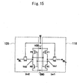
- An input/output characteristic of the first inverter 110 and an input/output characteristic of the second inverter 120 are obtained by applying a rated power source voltage VDD to word line W and bit lines BL, BL in the SRAM memory cell shown in Fig. 15 respectively.
- Fig. 16 shows the first inverter by extracting the first inverter from the SRAM memory cell shown in Fig. 15 .
- an output voltage outputted from a node Vs1 when an input voltage ranging from 0V to the rated power source voltage VDD is applied to a node Vs2 is obtained, and is used as the first input/output characteristic data.
- Fig. 17 shows an example of the first input/output characteristic data 130.
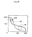
- an output voltage outputted from a node Vs2 when an input voltage ranging from 0V to the rated power source voltage VDD is applied to a node Vs1 in the second inverter 120 shown in Fig. 18 is obtained, and is used as the second input/output characteristic data.
- an X-Y axis conversion is performed by aligning the second input/output characteristic data with an axis of ordinate and an axis of abscissas of the first input/output characteristic data 130 thus newly forming the second input/output characteristic data.
- Fig. 19 shows an example of the second input/output characteristic data 140 obtained after the X-Y axis conversion.
- Patent document 1 JP-A-2005-310242
- Non-patent document 1 Evert Seevinck et al : "Static Noise Margin Analysis of MOS SRAM Cells" IEEE JOURNAL OF SOLID-STATE CIRCUITS, IEEE CENTER, PISCATAWAY, NJ, US vol. sc-22, no 5, 1 October 1987, pages 748-754 .
- a recent microminiaturized SRAM memory cell is liable to be influenced by various irregularities at the time of the manufacture of the SRAM memory cell along with such microminiaturization thus giving rise to a drawback that characteristics of two inverters which constitute a flip-flop of the SRAM memory cell do not match each other.
- the mismatch of characteristic of the inverters lowers the static noise margin value of the SRAM memory cell thus making a normal operation of the SRAM memory cell difficult.
- non-patent document 1 there is disclosed a method of calculating a static noise margin in which input/output characteristics (normal and mirror inverted with respect to X-Y axis) of two inverters constituting a SRAM flip-flop cell are rotated by 45 degrees, a difference of the output voltages is obtained, and a smaller value of the difference out of an absolute value of the minimum and the maximum is divided by square root of 2.
- the output voltages are obtained using a dc circuit simulator.
- inventors of the present invention have made extensive studies for realizing the designing of an SRAM memory cell which enables the evaluation of a static noise margin in a shorter time and is hardly influenced by various irregularities which may occur at the time of the manufacture of the SRAM memory cell, and have completed the present invention.
- a method for evaluating an SRAM memory cell according to claim 1 which stores data by a flip-flop circuit which is constituted of a first inverter and a second inverter, the method for evaluating an SRAM memory cell comprising the steps of: obtaining first input/output characteristic data which is a characteristic of an output voltage for an input voltage in the first inverter; obtaining second input/output characteristic data by applying X-Y axis conversion to characteristic data of an output voltage for an input voltage in the second inverter; generating first rotary converted data by applying coordinate conversion which rotates a coordinate axis by 45 degrees to the first input/output characteristic data; generating second rotary converted data by applying coordinate conversion which rotates a coordinate axis by 45 degrees to the second input/output characteristic data; specifying a first proximity curve function obtained by fitting the first rotary converted data to a proximity curve; specifying a second proximity curve function obtained by fitting the second
- a method for evaluating an SRAM memory cell and an evaluation program of an SRAM memory cell are based on a finding that a diagonal line of "a square which inscribes a predetermined region" is a value which is obtained by multiplying a value of a static noise margin by a square root of 2, and the diagonal line assumes the Y-axis direction due to the coordinate conversion which rotates the coordinate axis by 45 degrees.
- the coordinate conversion which rotates the coordinate axis by 45 degrees is applied to input/output characteristic data of a first inverter of the SRAM memory cell, and a first proximity curve function is specified by fitting the input/output characteristic data of a first inverter to a proximity curve.
- the coordinate conversion which rotates the coordinate axis by 45 degrees is applied to the X-Y axis-converted input/output characteristic data of a second inverter of the SRAM memory cell, and a second proximity curve function is specified by fitting the X-Y axis-converted input/output characteristic data to a proximity curve.
- a static noise margin can be specified based on an extremal value of a difference curve function which is the difference between the first proximity curve function and the second proximity curve function.
- the extremal value of the difference curve function is a value which is obtained by multiplying a value of the static noise margin by a square root of 2. That is, the value of the static noise margin can be calculated by dividing a smaller value between an absolute value of a minimum value and a maximum value out of the maximum value and the minimum value of the difference curve function by the square root of 2.
- steps of calculating the static noise margin can be simplified and hence, the evaluation of the static noise margin can be performed within an extremely short time thus shortening time necessary for designing the SRAM memory cell.
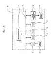
- the static noise margin is calculated using a computer 10 which includes a CPU 11 for executing predetermined arithmetic processing.
- the CPU 11 is connected to, via a bus 12, a ROM 13 which stores a predetermined program, a RAM 14 which develops the program to be executed or stores predetermined data, and a hard disk device 15 which stores an evaluation program of the SRAM memory cell, a simulation program for generating DC characteristic data of the SRAM memory cell and the like.
- the CPU 11 can execute predetermined processing.
- a recording medium for example, a CD-ROM, a DVD-ROM, a USB memory or the like in which a computer readable evaluation program is recorded may be used.
- an input means 17 such as a keyboard, a mouse or a tablet is connected via an input interface circuit 16.
- a display device 19 is connected via an image processing circuit 18 to allow the display device 19 to display a predetermined image.
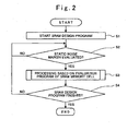
- the evaluation program of the SRAM memory cell according to this embodiment is operated as one subroutine in a design program of the SRAM memory cell stored in the hard disk device 15.
- step 1 based on a start command of a design program of the SRAM memory cell inputted from the input means 17, the design program of the SRAM memory cell is started (step 1) so that a design condition of the SRAM memory cell is inputted.
- a "static noise margin evaluation" button switch which is provided on a display screen of the display device 19 is selected by the input means 17 (step S2: YES) so that the computer 10 starts the evaluation program of the SRAM memory cell for executing the evaluation of the SRAM memory cell (step S3).
- the computer 10 executes the predetermined processing based on the design program of the SRAM memory cell.
- step S4 NO
- the computer 10 executes the predetermined processing based on the design program of the SRAM memory cell.
- the computer 10 executes following processing by starting the evaluation program of the SRAM memory cell in step S3.
- the computer 10 obtains a characteristic of an output voltage for an input voltage in one inverter out of two inverters which constitute the SRAM memory cell as first input/output characteristic data (step T1 in Fig. 3 ).
- first input/output characteristic data is indicated by white dots in Fig. 4 .
- the first input/output characteristic data which the computer obtains may be input/output characteristic data preliminarily stored in the RAM 14 or the hard disk device 15, or may be input/output characteristic data inputted by the input means 17 such as a keyboard, or may be input/output characteristic data which is read from a recording medium such as a memory card. Further, the first input/output characteristic data which the computer 10 obtains may be input/output characteristic data obtained by a simulation which is carried out by inputting the design condition of the SRAM memory cell. Still further, the first input/output characteristic data which the computer obtains may be input/output characteristic data obtained by measuring an actual device. This embodiment exemplifies a case where the simulation is carried out by inputting the design condition of the SRAM memory cell at the time of acquiring the first input/output characteristic data, and the input/output characteristic data obtained as a result of the simulation is used.
- a characteristic of an output voltage for an input voltage in the other inverter out of two inverters which constitute the SRAM memory cell is subject to the X-Y axis conversion, and the computer 10 obtains the characteristic of the output voltage as second input/output characteristic data (step T2 in Fig. 3 ).
- An example of the second input/output characteristic data is indicated by black dots in Fig. 4 .
- the second input/output characteristic data which the computer obtains may also be input/output characteristic data preliminarily stored in the RAM 14 or the hard disk device 15 or may be input/output characteristic data inputted by the input means 17 such as a keyboard, or may be input/output characteristic data which is read from a recording medium such as a memory card.
- the second input/output characteristic data which the computer obtains may be data obtained by a simulation or data obtained by measuring an actual device. In this embodiment, the simulation is carried out by inputting the design condition of the SRAM memory cell at the time of acquiring the second input/output characteristic data, and the input/output characteristic data obtained as a result of the simulation is used. In carrying out the simulation, the calculation of the first input/output characteristic data and the calculation of the second input/output characteristic data may be performed simultaneously thus acquiring the first input/output characteristic data and the second input/output characteristic data simultaneously.
- the computer 10 applies the coordinate conversion which rotates the coordinate axis by 45 degrees to the first input/output characteristic data so as to generate the first rotary converted data (step T3 in Fig. 3 ).
- An example of the first rotary converted data is indicated by white dots in Fig. 5 .
- the rotary conversion is an arithmetic operation which is carried out in accordance with following equations in which coordinates before rotation are set to (x,y), and the coordinates after rotation are set to (X,Y).
- X cos ⁇ / 4 ⁇ x - sin ⁇ / 4 ⁇ y
- Y sin ⁇ / 4 ⁇ x + cos ⁇ / 4 ⁇ y
- the computer 10 applies the coordinate conversion which rotates the coordinate axis by 45 degrees to the second input/output characteristic data so as to generate the second rotary converted data (step T4 in Fig. 3 ).
- Black dots in Fig. 5 indicate the second rotary converted data.
- the computer 10 After generation of respective rotary converted data, as shown in Fig. 6 , the computer 10 specifies a first proximity curve function L1 obtained by fitting the first rotary converted data to a proximity curve (step T5 in Fig. 3 ) and, at the same time, the computer 10 specifies a second proximity curve function L2 obtained by fitting the second rotary converted data to a proximity curve (step T6 in Fig. 3 ).
- the computer 10 executes a proximity curve specifying program for specifying the first proximity curve function L1 and the second proximity curve function L2.
- the first proximity curve function L1 and the second proximity curve function L2 are specified by the proximity curve specifying program which uses a least square method.
- the proximity curve specifying program fitting is performed by assuming the first proximity curve function L1 and the second proximity curve function L2 as a curve expressed by a cubic or more polynomial.
- a polynomial as a subject equation for fitting
- the calculation executed in step T6 and ensuing steps in Fig. 3 can be simplified.
- the reason that the order of polynomial is set to cubic or more is that, as can be understood from a shape of the rotary converted data shown in Fig. 5 or Fig. 6 , it is desirable to use an equation which has two or more extremal values as an equation for fitting.
- the computer 10 After specifying the respective proximity curve functions L1, L2, the computer 10 specifies a difference curve function which is the difference between the first proximity curve function L1 and the second proximity curve function L2 (step T7 in Fig. 3 ). This difference curve function is indicated by symbol L3 in Fig. 7 .
- the computer 10 After specifying the difference curve function L3, the computer 10 specifies a maximum value and a minimum value of the difference curve function L3 (step T8 in Fig. 3 ) and, at the same time, calculates a static noise margin (SNM) by dividing a smaller value out of an absolute value of the minimum value and the maximum value by a square root of 2 (step T9 in Fig: 3 ).
- SNM static noise margin
- a portion indicated by SNM x(square root symbol) 2 in the drawing corresponds to a value which is (square root of 2) times as large as a target static noise margin value.
- the difference curve function L3 is also formed of a quintic polynomial.
- the equation obtained by differentiating the quintic or lesser-order polynomial becomes a quaternary or lesser-order polynomial and hence, it is possible to use a formula of solution of a polynomial equation in the calculation of extremal values. Accordingly, the numerical value calculation is unnecessary, and it is possible to carry out the subsequent calculation more easily and at a higher speed than a case where fitting is made using other functions.
- step T10 in Fig. 3 YES
- the computer 10 returns to step T1 in Fig. 3 , obtains new first input/output characteristic data and the second input/output characteristic data and calculates a static noise margin.
- step T10 in Fig. 3 NO
- the computer 10 finishes the evaluation program of the SRAM memory cell and returns to the main routine.
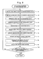
- FIG. 8 A flowchart of the second embodiment corresponding to the flowchart of the first embodiment shown in Fig. 3 is shown in Fig. 8 .
- two inverters which constitute an SRAM used in this embodiment are equal to the inverters used in the explanation of the first embodiment.
- the same terms are used and their explanation of the contents is omitted in the second specific embodiment.
- steps equal to the steps in the flowchart of the first embodiment are given same symbols.
- This embodiment is characterized in that, compared with the first specific embodiment where the second input/output characteristic data is obtained by applying the X-Y axis conversion to the characteristic of the output voltage for the input voltage in the other inverter in step T2 in Fig. 3 , the characteristic of the output voltage for the input voltage in the other inverter is directly used as the second input/output characteristic data without applying the X-Y axis conversion to the characteristic of the output voltage.
- the Y-axis inverted data is generated.
- the computer 10 obtains a characteristic of an output voltage for an input voltage in one inverter out of two inverters which constitute the SRAM memory cell as first input/output characteristic data (step T1 in Fig. 8 ).
- An example of the first input/output characteristic data is indicated by white dots in Fig. 9 .
- the first input/output characteristic data is equal to the first input/output characteristic data indicated by white dots in Fig. 5 .
- the computer 10 directly obtains the second input/output characteristic data which is the characteristic of an output voltage for the input voltage in the other inverter out of two inverters which constitute the SRAM memory cell without applying the X-Y axis conversion to the characteristic of the output voltage (step T2' in Fig. 8 ).
- Black dots in Fig. 9 indicate the second input/output characteristic data.
- the computer 10 After applying the rotary conversion which rotates a coordinate axis by 45 degrees to the respective coordinate point data of the first input/output characteristic data, the computer 10 generates the first rotary converted data by rotating the coordinate axis by 45 degrees with respect to the first input/output characteristic data (step T3 in Fig. 8 ).
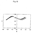
- White dots in Fig. 10 indicate the first rotary converted data.
- the rotary conversion is executed by performing the calculation in the same manner as the first embodiment.
- the computer 10 After applying the rotary conversion of which rotates a coordinate axis by 45 degrees to the respective coordinate point data of the second input/output characteristic data, the computer 10 generates the second rotary converted data by rotating the coordinate axis by 45 degrees with respect to the second input/output characteristic data (step T4 in Fig. 8 ). Black dots in Fig. 10 indicate the second rotary converted data.
- the first rotary converted data and the second rotary converted data it may be possible to adopt a method where a large number of input/output characteristic data with respect to inverters are preliminarily collected by taking the influence such as characteristic irregularities into consideration, two arbitrary input/output characteristic data are taken out when necessary, and set as the first and second input/output characteristic data, and the first and second rotary converted data are generated based on the first and second input/output characteristic data.
- the computer 10 executes the coordinate conversion for mirror-inverting the second rotary converted data with respect to the Y axis thus generating the Y-axis inverted data (step T4' in Fig. 8 ).
- a graph where the Y-axis inverted data and the first rotary converted data overlap with each other becomes the same graph as Fig. 5 in the first embodiment.
- the second embodiment makes use of a finding that an operation in which the X-Y-axis conversion is applied to the input/output characteristic data in step T2 in Fig. 3 and, thereafter, the coordinate conversion which rotates the coordinate axis by 45 degrees is performed in step T4, and an operation in which the coordinate conversion which rotates the coordinate axis by 45 degrees in step T4 in Fig. 8 and, thereafter, the Y-axis mirror inversion is performed in step T4' are equivalent to each other.
- This can be mathematically proved as follows.
- a matrix indicative of mapping which moves a point (x, y) to a point (x', y') by the coordinate conversion which rotates the coordinate axis by 45 degrees is expressed as follows.
- the coordinate conversion which performs the Y-axis mirror inversion after performing the coordinate conversion which rotates the coordinate axis by 45 degrees is expressed by a product of a matrix shown in the equation (2) and a matrix shown in the equation (3).
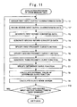
- This embodiment is characterized in that, compared to the second specific embodiment where the coordinate conversion which performs mirror inversion with respect to the Y axis is applied to the second rotary converted data in step T4' in Fig. 8 thus generating the Y-axis inverted data, a third proximity curve function is generated by mirror-inverting the second proximity curve function in place of the second rotary converted data.
- the difference function is generated using the first rotary converted data and the third proximity curve function obtained by mirror-inverting the second proximity curve function.
- Fig. 11 shows a flowchart of the third embodiment corresponding to the flowchart of the first embodiment shown in Fig. 3 .
- step T4 in Fig. 11 advances completely in the same manner as the processing up to step T4 in the flowchart of the second embodiment shown in Fig. 8 and hence, the explanation of such processing is omitted.
- two inverters which constitute an SRAM memory cell used in this embodiment are equal to the inverters used in the explanation of the second embodiment.
- steps equal to the steps in the flowchart of the second embodiment are given the same symbols.
- a graph obtained as a result of step T4 in Fig. 11 is equal to the graph shown in Fig. 10 obtained as the result of step T4 in Fig. 8 .
- the computer 10 without performing the coordinate conversion which mirror-inverts the second rotary converted data with respect to the Y axis in step T4' in Fig. 8 , specifies the first proximity curve function and the second proximity curve function respectively using a fitting technique substantially equal to the fitting technique used in the first embodiment based on the first rotary converted data and the second rotary converted data (steps T5, T6 in Fig. 11 ). Also in these steps, it is effective to use a cubic or more polynomial, and more particularly, a quintic polynomial as an equation used for fitting.
- the first proximity curve function and the second proximity curve function obtained as a result of the fitting are indicated by a broken line (L1) and a solid line (L2) in Fig. 12 respectively.
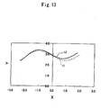
- Fig. 13 shows a graph which is prepared by deleting the original rotary converted data and extracting only the first proximity curve function (L1) and the second proximity curve function (L2) from Fig. 12 .
- L1 and L2 are expressed by following functional forms respectively.
- Y a 1 ⁇ X 5 + b 1 ⁇ X 4 + c 1 ⁇ X 3 + d 1 ⁇ X 2 + e 1 ⁇ X + f 1
- Y a 2 ⁇ X 5 + b 2 ⁇ X 4 + c 2 ⁇ X 3 + d 2 ⁇ X 2 + e 2 ⁇ X + f 2
- a 1 , a 2 , b 1 , b 2 , c 1 , c 2 , d 1 , d 2 , e 1 , e 2 , f 1 , f 2 are parameters determined corresponding to the fitting.
- the computer 10 generates the third proximity curve function by mirror-inverting the second proximity curve function L2 with respect to the Y axis in Fig. 13 (step T6' in Fig. 11 ).
- This Y-axis mirror-inversion operation is equivalent to an operation which substitutes X with -X in the above-mentioned equation (7). That is, this operation is equal to an operation to change signs in front of parameters a 2 , c 2 , e 2 to "-".
- Fig. 14 is a graph which is drawn by overlapping L2' obtained as a result of the Y-axis mirror inversion with L1.
- step T7 in Fig. 11 Subsequent steps ranging from specifying of the difference curve function (step T7 in Fig. 11 ) to the calculation of the static noise margin are substantially equal to step T7 and ensuing steps in Fig. 8 and hence, the explanation of the steps is omitted.
- the Y-axis mirror inversion operation can be instantaneously performed using the equation (8).
- the equation (8) it is possible to describe the input/output characteristic of the inverters using only six parameters consisting of a 1 to f 1 and hence, it is possible to form basic and necessary minimum data base with respect to the SRAM memory cell circuit design with the small amount of data.
- the static noise margin with respect to various SRAM memory cells can be instantaneously calculated thus easily realizing the acquisition of an optimum memory cell circuit.
Landscapes
- Engineering & Computer Science (AREA)
- Microelectronics & Electronic Packaging (AREA)
- Computer Hardware Design (AREA)
- Semiconductor Memories (AREA)
- For Increasing The Reliability Of Semiconductor Memories (AREA)
- Static Random-Access Memory (AREA)
- Tests Of Electronic Circuits (AREA)
Claims (4)
- Verfahren zum Evaluieren einer SRAM-Speicherzelle, die Daten durch eine Flip-Flop-Schaltung speichert, die aus einem ersten Inverter und einem zweiten Inverter besteht, wobei das Verfahren zum Evaluieren einer SRAM-Speicherzelle die folgenden Schritte umfasst:Erhalten von ersten charakteristischen Eingangs-/Ausgangsdaten, die eine Charakteristik einer Ausgangsspannung für eine Eingangsspannung an dem ersten Inverter (T1) sind;Erhalten von zweiten charakteristischen Eingangs-/Ausgangsdaten durch Anwenden einer X-Y-Achsenkonversion auf charakteristische Daten einer Ausgangsspannung für eine Eingangsspannung an dem zweiten Inverter (T2);Erzeugen von ersten drehkonvertierten Daten durch Anwenden einer Koordinatenkonversion, die eine Koordinatenachse um 45 Grad zu den ersten charakteristischen Eingangs-/Ausgangsdaten (T3) dreht;Erzeugen von zweiten drehumgesetzten Daten durch Anwenden einer Koordinatenkonversion, die eine Koordinatenachse um 45 Grad zu den zweiten charakteristischen Eingangs-/Ausgangsdaten (T4) dreht;wobei das Verfahren dadurch gekennzeichnet ist, dass es die folgenden Schritte umfasst:Spezifizieren einer ersten Näherungskurvenfunktion, die durch Anpassen der ersten drehkonvertierten Daten an eine Näherungskurve (T5) erhalten wird;Spezifizieren einer zweiten Näherungskurvenfunktion, die durch Anpassen der zweiten drehkonvertierten Daten an eine Näherungskurve (T6) erhalten wird;Spezifizieren einer Differenzkurvenfunktion, die die Differenz zwischen der ersten Näherungskurvenfunktion und der zweiten Näherungskurvenfunktion (T7) ist;Spezifizieren eines maximalen Wertes und eines minimalen Wertes der Differenzkurvenfunktion (T8) undBerechnen eines statischen Rauschbereichs durch Dividieren des kleineren Wertes eines Absolutwerts des minimalen Wertes und des maximalen Wertes durch die Wurzel von 2 (T9),wobeidie erste Näherungskurvenfunktion, die zweite Näherungskurvenfunktion und die Differenzkurvenfunktion eine Funktion sind, die durch ein Polynom fünfter oder niedrigerer Ordnung ausgedrückt wird.
- Verfahren zum Evaluieren einer SRAM-Speicherzelle nach Anspruch 1,
wobei ein Schritt (T4') des Erzeugens von Y-achsen-invertierten Daten durch Spiegelinvertieren der zweiten drehkonvertierten Daten in Bezug auf eine YAchse nach dem Schritt (T4) des Erzeugens der zweiten drehkonvertierten Daten eingefügt wird und
wobei die zweiten charakteristischen Daten einer Charakteristik einer Ausgangsspannung für eine Eingangsspannung an dem zweiten Inverter (T2') anstelle der zweiten charakteristischen Eingangs-/Ausgangsdaten, die durch Anwenden einer X-Y-Achsenkonversion an den charakteristischen Daten einer Ausgangsspannung für eine Eingangsspannung an dem zweiten Inverter erhalten werden, entsprechen. - Verfahren zum Evaluieren einer SRAM-Speicherzelle nach Anspruch 1, wobei
ein Schritt (T6') des Erhaltens einer dritten Näherungskurvenfunktion, die eine spiegelinvertierte Funktion der zweiten Näherungskurve in Bezug auf eine YAchse ist und
ein Schritt des Spezifizierens einer Differenzkurvenfunktion, wobei die Differenz zwischen der ersten Näherungskurvenfunktion und der dritten Näherungskurvenfunktion besteht, anstelle des Schrittes des Spezifizierens einer Differenzkurvenfunktion, die die Differenz zwischen der ersten Näherungskurvenfunktion und der zweiten Näherungskurvenfunktion ist, nach dem Schritt (T6) des Spezifizierens einer zweiten Näherungskurvenfunktion eingefügt ist und wobei die zweiten charakteristischen Daten einer Charakteristik einer Ausgangsspannung für eine Eingangsspannung an dem zweiten Inverter (T2') anstelle der zweiten charakteristischen Eingangs-/Ausgangsdaten, die durch Anwenden einer X-Y-Achsenkonversion auf die charakteristischen Daten einer Ausgangsspannung für eine Eingangsspannung an dem zweiten Inverter erhalten werden, entsprechen. - Computerlesbares Aufzeichnungsmedium, das ein Programm umfasst, das ausgelegt ist, das Verfahren nach einem der Ansprüche 1 bis 3 auszuführen.
Applications Claiming Priority (2)
| Application Number | Priority Date | Filing Date | Title |
|---|---|---|---|
| JP2007095928A JP4411443B2 (ja) | 2007-03-31 | 2007-03-31 | Sramメモリセルの評価方法及びsramメモリセルの評価プログラム |
| PCT/JP2008/054308 WO2008126548A1 (ja) | 2007-03-31 | 2008-03-10 | Sramメモリセルの評価方法及びsramメモリセルの評価プログラムをコンピュータが読み取り可能に記録した記録媒体 |
Publications (3)
| Publication Number | Publication Date |
|---|---|
| EP2136372A1 EP2136372A1 (de) | 2009-12-23 |
| EP2136372A4 EP2136372A4 (de) | 2010-04-21 |
| EP2136372B1 true EP2136372B1 (de) | 2014-12-03 |
Family
ID=39863700
Family Applications (1)
| Application Number | Title | Priority Date | Filing Date |
|---|---|---|---|
| EP08721724.6A Not-in-force EP2136372B1 (de) | 2007-03-31 | 2008-03-10 | Verfahren zur evaluierung einer sram-speicherzelle und medium, das ein evaluierungsprogramm für eine sram-speicherzelle computerlesbar aufzeichnet |
Country Status (5)
| Country | Link |
|---|---|
| US (1) | US8169813B2 (de) |
| EP (1) | EP2136372B1 (de) |
| JP (1) | JP4411443B2 (de) |
| KR (1) | KR101452013B1 (de) |
| WO (1) | WO2008126548A1 (de) |
Families Citing this family (2)
| Publication number | Priority date | Publication date | Assignee | Title |
|---|---|---|---|---|
| WO2013109003A1 (ko) * | 2012-01-20 | 2013-07-25 | 연세대학교 산학협력단 | 정적 램의 수율 추정 방법 및 정적 램의 수율 추정 장치 |
| KR101385109B1 (ko) | 2012-01-20 | 2014-04-16 | 연세대학교 산학협력단 | 정적 램의 수율 추정 방법 및 정적 램의 수율 추정 장치 |
Family Cites Families (4)
| Publication number | Priority date | Publication date | Assignee | Title |
|---|---|---|---|---|
| JP2841665B2 (ja) | 1990-03-23 | 1998-12-24 | 三菱電機株式会社 | スタティックram |
| CN100437834C (zh) | 2003-03-12 | 2008-11-26 | Nxp股份有限公司 | 用于弱sram单元的检测装置和方法 |
| JP2005310242A (ja) | 2004-04-20 | 2005-11-04 | Matsushita Electric Ind Co Ltd | Sramメモリセルの評価方法 |
| JP4256327B2 (ja) | 2004-11-05 | 2009-04-22 | 株式会社東芝 | スタティックランダムアクセスメモリ、および擬似スタティックノイズマージンの計測方法 |
-
2007
- 2007-03-31 JP JP2007095928A patent/JP4411443B2/ja active Active
-
2008
- 2008-03-10 WO PCT/JP2008/054308 patent/WO2008126548A1/ja not_active Ceased
- 2008-03-10 KR KR1020097022739A patent/KR101452013B1/ko not_active Expired - Fee Related
- 2008-03-10 US US12/594,048 patent/US8169813B2/en not_active Expired - Fee Related
- 2008-03-10 EP EP08721724.6A patent/EP2136372B1/de not_active Not-in-force
Non-Patent Citations (1)
| Title |
|---|
| SEEVINCK E ET AL: "Static-Noise Margin Analysis of MOS SRAM Cells", IEEE JOURNAL OF SOLID-STATE CIRCUITS, IEEE SERVICE CENTER, PISCATAWAY, NJ, US LNKD- DOI:10.1109/JSSC.1987.1052809, vol. SC-22, no. 5, 1 October 1987 (1987-10-01), pages 748 - 754, XP002178159, ISSN: 0018-9200 * |
Also Published As
| Publication number | Publication date |
|---|---|
| EP2136372A1 (de) | 2009-12-23 |
| US20100115352A1 (en) | 2010-05-06 |
| JP4411443B2 (ja) | 2010-02-10 |
| KR101452013B1 (ko) | 2014-10-21 |
| KR20100016077A (ko) | 2010-02-12 |
| WO2008126548A1 (ja) | 2008-10-23 |
| US8169813B2 (en) | 2012-05-01 |
| EP2136372A4 (de) | 2010-04-21 |
| JP2008257760A (ja) | 2008-10-23 |
Similar Documents
| Publication | Publication Date | Title |
|---|---|---|
| US9355212B2 (en) | MEMS modeling system and method | |
| US8510699B1 (en) | Performance driven layout optimization using morphing of a basis set of representative layouts | |
| US7065731B2 (en) | Removal of acute angles in a design layout | |
| US12169671B2 (en) | Apparatus and method for mapping foundational components during design porting from one process technology to another process technology | |
| US8341566B2 (en) | Method for generating and evaluating a table model for circuit simulation | |
| US10331838B2 (en) | Semiconductor device with fill cells | |
| US10430546B2 (en) | Integrated circuit, and computing system and computer-implemented method for designing integrated circuit | |
| KR20230041017A (ko) | 상보형 전계 효과 트랜지스터(cfet)에서의 소스 및 드레인 재료들의 에피택셜 성장 | |
| EP2136372B1 (de) | Verfahren zur evaluierung einer sram-speicherzelle und medium, das ein evaluierungsprogramm für eine sram-speicherzelle computerlesbar aufzeichnet | |
| CN117521574A (zh) | 基于模块化策略的中间表示层扫描链插入方法及系统 | |
| CN109902318B (zh) | 生成标准延时格式文件的方法和装置 | |
| Qiao et al. | Variability-aware compact modeling and statistical circuit validation on SRAM test array | |
| US5896303A (en) | Discretization technique for multi-dimensional semiconductor device simulation | |
| JP2006023873A (ja) | 半導体集積回路の設計方法、その設計支援装置及び遅延ライブラリ | |
| DE102020115583A1 (de) | Hierarchischer graphenbasierter domänenauswahlalgorithmus zum verbessern der diversität | |
| DE102020120157A1 (de) | Einstufen von objekten mit rauschbehafteten messungen | |
| US8176455B2 (en) | Semiconductor device design support apparatus and substrate netlist generation method | |
| US7080339B2 (en) | Plane representation of wiring in a design layout | |
| US10169524B2 (en) | Universal cell model for array and circuit simulation using the same | |
| TWI499924B (zh) | 供影像與cad對準使用之p型區域及n型區域差異化 | |
| US20080244481A1 (en) | Method for designing and manufacturing semiconductor device and software therefor | |
| CN111292396B (zh) | 图像样本集生成方法、设备、装置及存储介质 | |
| Gavrilov et al. | Methods of accelerated characterization of VLSI cell libraries with prescribed accuracy control | |
| CN113327643B (zh) | 工艺角检测方法及系统、设备、存储介质 | |
| US7143370B1 (en) | Parameter linking system for data visualization in integrated circuit technology development |
Legal Events
| Date | Code | Title | Description |
|---|---|---|---|
| PUAI | Public reference made under article 153(3) epc to a published international application that has entered the european phase |
Free format text: ORIGINAL CODE: 0009012 |
|
| 17P | Request for examination filed |
Effective date: 20091102 |
|
| AK | Designated contracting states |
Kind code of ref document: A1 Designated state(s): AT BE BG CH CY CZ DE DK EE ES FI FR GB GR HR HU IE IS IT LI LT LU LV MC MT NL NO PL PT RO SE SI SK TR |
|
| A4 | Supplementary search report drawn up and despatched |
Effective date: 20100323 |
|
| RIC1 | Information provided on ipc code assigned before grant |
Ipc: G11C 29/50 20060101AFI20100317BHEP |
|
| RIC1 | Information provided on ipc code assigned before grant |
Ipc: G11C 29/50 20060101AFI20100518BHEP |
|
| DAX | Request for extension of the european patent (deleted) | ||
| 17Q | First examination report despatched |
Effective date: 20100618 |
|
| GRAP | Despatch of communication of intention to grant a patent |
Free format text: ORIGINAL CODE: EPIDOSNIGR1 |
|
| INTG | Intention to grant announced |
Effective date: 20140627 |
|
| GRAP | Despatch of communication of intention to grant a patent |
Free format text: ORIGINAL CODE: EPIDOSNIGR1 |
|
| GRAS | Grant fee paid |
Free format text: ORIGINAL CODE: EPIDOSNIGR3 |
|
| GRAA | (expected) grant |
Free format text: ORIGINAL CODE: 0009210 |
|
| INTG | Intention to grant announced |
Effective date: 20141017 |
|
| AK | Designated contracting states |
Kind code of ref document: B1 Designated state(s): AT BE BG CH CY CZ DE DK EE ES FI FR GB GR HR HU IE IS IT LI LT LU LV MC MT NL NO PL PT RO SE SI SK TR |
|
| REG | Reference to a national code |
Ref country code: GB Ref legal event code: FG4D |
|
| REG | Reference to a national code |
Ref country code: CH Ref legal event code: EP Ref country code: AT Ref legal event code: REF Ref document number: 699771 Country of ref document: AT Kind code of ref document: T Effective date: 20141215 |
|
| REG | Reference to a national code |
Ref country code: IE Ref legal event code: FG4D |
|
| REG | Reference to a national code |
Ref country code: DE Ref legal event code: R096 Ref document number: 602008035672 Country of ref document: DE Effective date: 20150115 |
|
| REG | Reference to a national code |
Ref country code: NL Ref legal event code: VDEP Effective date: 20141203 |
|
| REG | Reference to a national code |
Ref country code: AT Ref legal event code: MK05 Ref document number: 699771 Country of ref document: AT Kind code of ref document: T Effective date: 20141203 |
|
| PG25 | Lapsed in a contracting state [announced via postgrant information from national office to epo] |
Ref country code: FI Free format text: LAPSE BECAUSE OF FAILURE TO SUBMIT A TRANSLATION OF THE DESCRIPTION OR TO PAY THE FEE WITHIN THE PRESCRIBED TIME-LIMIT Effective date: 20141203 Ref country code: NO Free format text: LAPSE BECAUSE OF FAILURE TO SUBMIT A TRANSLATION OF THE DESCRIPTION OR TO PAY THE FEE WITHIN THE PRESCRIBED TIME-LIMIT Effective date: 20150303 Ref country code: LT Free format text: LAPSE BECAUSE OF FAILURE TO SUBMIT A TRANSLATION OF THE DESCRIPTION OR TO PAY THE FEE WITHIN THE PRESCRIBED TIME-LIMIT Effective date: 20141203 Ref country code: NL Free format text: LAPSE BECAUSE OF FAILURE TO SUBMIT A TRANSLATION OF THE DESCRIPTION OR TO PAY THE FEE WITHIN THE PRESCRIBED TIME-LIMIT Effective date: 20141203 Ref country code: ES Free format text: LAPSE BECAUSE OF FAILURE TO SUBMIT A TRANSLATION OF THE DESCRIPTION OR TO PAY THE FEE WITHIN THE PRESCRIBED TIME-LIMIT Effective date: 20141203 |
|
| REG | Reference to a national code |
Ref country code: LT Ref legal event code: MG4D |
|
| PG25 | Lapsed in a contracting state [announced via postgrant information from national office to epo] |
Ref country code: HR Free format text: LAPSE BECAUSE OF FAILURE TO SUBMIT A TRANSLATION OF THE DESCRIPTION OR TO PAY THE FEE WITHIN THE PRESCRIBED TIME-LIMIT Effective date: 20141203 Ref country code: GR Free format text: LAPSE BECAUSE OF FAILURE TO SUBMIT A TRANSLATION OF THE DESCRIPTION OR TO PAY THE FEE WITHIN THE PRESCRIBED TIME-LIMIT Effective date: 20150304 Ref country code: SE Free format text: LAPSE BECAUSE OF FAILURE TO SUBMIT A TRANSLATION OF THE DESCRIPTION OR TO PAY THE FEE WITHIN THE PRESCRIBED TIME-LIMIT Effective date: 20141203 Ref country code: AT Free format text: LAPSE BECAUSE OF FAILURE TO SUBMIT A TRANSLATION OF THE DESCRIPTION OR TO PAY THE FEE WITHIN THE PRESCRIBED TIME-LIMIT Effective date: 20141203 Ref country code: LV Free format text: LAPSE BECAUSE OF FAILURE TO SUBMIT A TRANSLATION OF THE DESCRIPTION OR TO PAY THE FEE WITHIN THE PRESCRIBED TIME-LIMIT Effective date: 20141203 Ref country code: CY Free format text: LAPSE BECAUSE OF FAILURE TO SUBMIT A TRANSLATION OF THE DESCRIPTION OR TO PAY THE FEE WITHIN THE PRESCRIBED TIME-LIMIT Effective date: 20141203 |
|
| PG25 | Lapsed in a contracting state [announced via postgrant information from national office to epo] |
Ref country code: SK Free format text: LAPSE BECAUSE OF FAILURE TO SUBMIT A TRANSLATION OF THE DESCRIPTION OR TO PAY THE FEE WITHIN THE PRESCRIBED TIME-LIMIT Effective date: 20141203 Ref country code: PT Free format text: LAPSE BECAUSE OF FAILURE TO SUBMIT A TRANSLATION OF THE DESCRIPTION OR TO PAY THE FEE WITHIN THE PRESCRIBED TIME-LIMIT Effective date: 20150403 Ref country code: CZ Free format text: LAPSE BECAUSE OF FAILURE TO SUBMIT A TRANSLATION OF THE DESCRIPTION OR TO PAY THE FEE WITHIN THE PRESCRIBED TIME-LIMIT Effective date: 20141203 Ref country code: RO Free format text: LAPSE BECAUSE OF FAILURE TO SUBMIT A TRANSLATION OF THE DESCRIPTION OR TO PAY THE FEE WITHIN THE PRESCRIBED TIME-LIMIT Effective date: 20141203 Ref country code: EE Free format text: LAPSE BECAUSE OF FAILURE TO SUBMIT A TRANSLATION OF THE DESCRIPTION OR TO PAY THE FEE WITHIN THE PRESCRIBED TIME-LIMIT Effective date: 20141203 |
|
| PG25 | Lapsed in a contracting state [announced via postgrant information from national office to epo] |
Ref country code: PL Free format text: LAPSE BECAUSE OF FAILURE TO SUBMIT A TRANSLATION OF THE DESCRIPTION OR TO PAY THE FEE WITHIN THE PRESCRIBED TIME-LIMIT Effective date: 20141203 Ref country code: IS Free format text: LAPSE BECAUSE OF FAILURE TO SUBMIT A TRANSLATION OF THE DESCRIPTION OR TO PAY THE FEE WITHIN THE PRESCRIBED TIME-LIMIT Effective date: 20150403 |
|
| REG | Reference to a national code |
Ref country code: DE Ref legal event code: R097 Ref document number: 602008035672 Country of ref document: DE |
|
| PLBE | No opposition filed within time limit |
Free format text: ORIGINAL CODE: 0009261 |
|
| STAA | Information on the status of an ep patent application or granted ep patent |
Free format text: STATUS: NO OPPOSITION FILED WITHIN TIME LIMIT |
|
| PG25 | Lapsed in a contracting state [announced via postgrant information from national office to epo] |
Ref country code: LU Free format text: LAPSE BECAUSE OF FAILURE TO SUBMIT A TRANSLATION OF THE DESCRIPTION OR TO PAY THE FEE WITHIN THE PRESCRIBED TIME-LIMIT Effective date: 20150310 Ref country code: DK Free format text: LAPSE BECAUSE OF FAILURE TO SUBMIT A TRANSLATION OF THE DESCRIPTION OR TO PAY THE FEE WITHIN THE PRESCRIBED TIME-LIMIT Effective date: 20141203 Ref country code: MC Free format text: LAPSE BECAUSE OF FAILURE TO SUBMIT A TRANSLATION OF THE DESCRIPTION OR TO PAY THE FEE WITHIN THE PRESCRIBED TIME-LIMIT Effective date: 20141203 |
|
| REG | Reference to a national code |
Ref country code: CH Ref legal event code: PL |
|
| 26N | No opposition filed |
Effective date: 20150904 |
|
| GBPC | Gb: european patent ceased through non-payment of renewal fee |
Effective date: 20150310 |
|
| PG25 | Lapsed in a contracting state [announced via postgrant information from national office to epo] |
Ref country code: IT Free format text: LAPSE BECAUSE OF FAILURE TO SUBMIT A TRANSLATION OF THE DESCRIPTION OR TO PAY THE FEE WITHIN THE PRESCRIBED TIME-LIMIT Effective date: 20141203 |
|
| REG | Reference to a national code |
Ref country code: FR Ref legal event code: ST Effective date: 20151130 |
|
| REG | Reference to a national code |
Ref country code: IE Ref legal event code: MM4A |
|
| PG25 | Lapsed in a contracting state [announced via postgrant information from national office to epo] |
Ref country code: LI Free format text: LAPSE BECAUSE OF NON-PAYMENT OF DUE FEES Effective date: 20150331 Ref country code: CH Free format text: LAPSE BECAUSE OF NON-PAYMENT OF DUE FEES Effective date: 20150331 Ref country code: GB Free format text: LAPSE BECAUSE OF NON-PAYMENT OF DUE FEES Effective date: 20150310 Ref country code: IE Free format text: LAPSE BECAUSE OF NON-PAYMENT OF DUE FEES Effective date: 20150310 |
|
| PG25 | Lapsed in a contracting state [announced via postgrant information from national office to epo] |
Ref country code: FR Free format text: LAPSE BECAUSE OF NON-PAYMENT OF DUE FEES Effective date: 20150331 Ref country code: SI Free format text: LAPSE BECAUSE OF FAILURE TO SUBMIT A TRANSLATION OF THE DESCRIPTION OR TO PAY THE FEE WITHIN THE PRESCRIBED TIME-LIMIT Effective date: 20141203 |
|
| PG25 | Lapsed in a contracting state [announced via postgrant information from national office to epo] |
Ref country code: BE Free format text: LAPSE BECAUSE OF FAILURE TO SUBMIT A TRANSLATION OF THE DESCRIPTION OR TO PAY THE FEE WITHIN THE PRESCRIBED TIME-LIMIT Effective date: 20141203 |
|
| PG25 | Lapsed in a contracting state [announced via postgrant information from national office to epo] |
Ref country code: MT Free format text: LAPSE BECAUSE OF FAILURE TO SUBMIT A TRANSLATION OF THE DESCRIPTION OR TO PAY THE FEE WITHIN THE PRESCRIBED TIME-LIMIT Effective date: 20141203 |
|
| PGFP | Annual fee paid to national office [announced via postgrant information from national office to epo] |
Ref country code: DE Payment date: 20170307 Year of fee payment: 10 |
|
| PG25 | Lapsed in a contracting state [announced via postgrant information from national office to epo] |
Ref country code: HU Free format text: LAPSE BECAUSE OF FAILURE TO SUBMIT A TRANSLATION OF THE DESCRIPTION OR TO PAY THE FEE WITHIN THE PRESCRIBED TIME-LIMIT; INVALID AB INITIO Effective date: 20080310 Ref country code: BG Free format text: LAPSE BECAUSE OF FAILURE TO SUBMIT A TRANSLATION OF THE DESCRIPTION OR TO PAY THE FEE WITHIN THE PRESCRIBED TIME-LIMIT Effective date: 20141203 |
|
| PG25 | Lapsed in a contracting state [announced via postgrant information from national office to epo] |
Ref country code: TR Free format text: LAPSE BECAUSE OF FAILURE TO SUBMIT A TRANSLATION OF THE DESCRIPTION OR TO PAY THE FEE WITHIN THE PRESCRIBED TIME-LIMIT Effective date: 20141203 |
|
| REG | Reference to a national code |
Ref country code: DE Ref legal event code: R119 Ref document number: 602008035672 Country of ref document: DE |
|
| PG25 | Lapsed in a contracting state [announced via postgrant information from national office to epo] |
Ref country code: DE Free format text: LAPSE BECAUSE OF NON-PAYMENT OF DUE FEES Effective date: 20181002 |