EP2129205A1 - Plasma display device - Google Patents
Plasma display device Download PDFInfo
- Publication number
- EP2129205A1 EP2129205A1 EP09157685A EP09157685A EP2129205A1 EP 2129205 A1 EP2129205 A1 EP 2129205A1 EP 09157685 A EP09157685 A EP 09157685A EP 09157685 A EP09157685 A EP 09157685A EP 2129205 A1 EP2129205 A1 EP 2129205A1
- Authority
- EP
- European Patent Office
- Prior art keywords
- heat dissipating
- dissipating plate
- display device
- switch
- chassis base
- Prior art date
- Legal status (The legal status is an assumption and is not a legal conclusion. Google has not performed a legal analysis and makes no representation as to the accuracy of the status listed.)
- Withdrawn
Links
Images


Classifications
-
- H—ELECTRICITY
- H01—ELECTRIC ELEMENTS
- H01J—ELECTRIC DISCHARGE TUBES OR DISCHARGE LAMPS
- H01J11/00—Gas-filled discharge tubes with alternating current induction of the discharge, e.g. alternating current plasma display panels [AC-PDP]; Gas-filled discharge tubes without any main electrode inside the vessel; Gas-filled discharge tubes with at least one main electrode outside the vessel
- H01J11/20—Constructional details
- H01J11/46—Connecting or feeding means, e.g. leading-in conductors
-
- H—ELECTRICITY
- H05—ELECTRIC TECHNIQUES NOT OTHERWISE PROVIDED FOR
- H05K—PRINTED CIRCUITS; CASINGS OR CONSTRUCTIONAL DETAILS OF ELECTRIC APPARATUS; MANUFACTURE OF ASSEMBLAGES OF ELECTRICAL COMPONENTS
- H05K7/00—Constructional details common to different types of electric apparatus
- H05K7/20—Modifications to facilitate cooling, ventilating, or heating
- H05K7/20954—Modifications to facilitate cooling, ventilating, or heating for display panels
- H05K7/20963—Heat transfer by conduction from internal heat source to heat radiating structure
-
- H—ELECTRICITY
- H01—ELECTRIC ELEMENTS
- H01J—ELECTRIC DISCHARGE TUBES OR DISCHARGE LAMPS
- H01J17/00—Gas-filled discharge tubes with solid cathode
- H01J17/02—Details
- H01J17/28—Cooling arrangements
Definitions
- the present invention relates to a display device, and more particularly, to a plasma display device with a switch.
- a plasma display device includes a plasma display panel (PDP), a chassis base supporting the PDP, a plurality of printed circuit boards installed on the chassis base, and a front cover and a back cover combined with the chassis base to embed or house the above constituent elements.
- PDP plasma display panel
- chassis base supporting the PDP
- PDP printed circuit boards
- front cover and a back cover combined with the chassis base to embed or house the above constituent elements.
- the PDP displays an image using visible light of red (R), green (G), and blue (B) generated by exciting phosphors using vacuum ultra-violet (VUV) rays emitted from plasmas obtained by a gas discharge.
- R visible light
- G green
- B blue
- VUV vacuum ultra-violet
- a sustain board and a scan board include switches to generate signals to be applied to a sustain electrode and a scan electrode included in the PDP. Since the switch generates a high frequency voltage pulse signal, the switch generates intense heat during operation.
- one surface of the printed circuit board is installed on the rear surface of the chassis base and the other surface of the printed circuit board includes various types of electrical elements and the switch.
- a heat sink may be attached onto the switch. The switch and the heat sink protrude from the printed circuit board.
- the heat sink may have some limitations on dissipating heat generated from the switch. In order to sufficiently dissipate the heat from the switch, the switch needs to be relatively large to increase the heat dissipation capacity.
- the back cover provided on the chassis base covering the printed circuit board side is formed to provide sufficient space for accommodating the printed circuit board, the switch, and the heat sink, resulting in increased thickness of the plasma display device.
- the switch since the switch is mounted on the printed circuit board toward the back cover, the switch emits electromagnetic interference (EMI) and noise to the outside of the back cover. Consequently, operation of the switch increases EMI and noise.
- EMI electromagnetic interference
- Embodiments of the present invention provide a plasma display device having advantages of reducing electromagnetic interference (EMI) and noise, and also improving heat dissipation performance of a switch and minimizing a thickness of a plasma display panel.
- EMI electromagnetic interference
- a display device includes a display panel for displaying an image, a chassis base for supporting the display panel and a heat dissipating plate at one side of the chassis base.
- the display device further includes a printed circuit board between the heat dissipating plate and the chassis base attached to the heat dissipating plate and electrically connected to the display panel, and a switch electrically connected to the printed circuit board adapted to generate a driving signal for controlling the display panel.
- the switch is attached to the heat dissipating plate.
- the chassis base further includes a plurality of bosses, wherein the heat dissipating plate is installed on the plurality of bosses.
- the heat dissipating plate may include a plurality of bosses adapted to support the printed circuit board and an installation hole aligned with the switch.
- the printed circuit board may include a first circuit pattern facing the chassis base and a second circuit pattern facing the heat dissipating plate, and the switch may be electrically connected to the second circuit pattern.
- the printed circuit board may include a penetration hole aligned with the installation hole of the heat dissipating plate.
- a heat sink may be on an outer surface of the heat dissipating plate or on the inner surface of the heat dissipating plate on which the switch is installed.
- the switch may also be arranged between the inner surface of the heat dissipating plate and the heat sink.
- the heat dissipating plate includes a plane portion generally parallel to the chassis base, a side portion curved from the plane portion toward the chassis base, and a flange curved from the side portion to be parallel to the plane portion and proximate an outer edge of the chassis base.
- the switch may be installed on an inner surface of the side portion and the display device may further include a heat sink on an outer surface of the side portion.
- the switch is a dual in-line package (DIP) type.
- the display panel is a plasma display panel.
- the printed circuit board may be a scan board comprising a scan electrode driver or a sustain board comprising a sustain electrode driver.
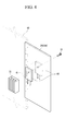
- FIG. 1 is an exploded perspective view of a plasma display device 100 according to a first embodiment of the present invention.
- the plasma display device 100 includes a plasma display panel (PDP) 10 for displaying an image, a chassis base 20, a heat dissipating plate 40, and a plurality of printed circuit boards 50.
- PDP plasma display panel
- the chassis base 20 supports the PDP and is attached to an opposite side of the PDP 10 from the display side of the PDP 10.
- the heat dissipating plate 40 is disposed at and attached to the rear of the chassis base 20.
- the chassis base 20 includes a plurality of bosses 21 separated from each other for receiving the heat dissipating plate 40.
- the heat dissipating plate 40 may be fastened to the bosses 21 by screws 22 or by other suitable fasteners.
- the printed circuit boards 50 are disposed between the chassis base 20 and the heat dissipating plate 40 and attached to the heat dissipating plate 40. Also, the printed circuit boards 50 may be electrically connected to the PDP 10 to operate the PDP 10.
- the present embodiment is primarily directed to the relationship between the heat dissipating plate 40 and the printed circuit board 50. Therefore, further detailed descriptions about the PDP 10 and the printed circuit board 50 will be omitted herein.
- the PDP 10 includes electrodes for gas discharge, for example, a sustain electrode (not shown), a scan electrode (not shown), and an address electrode (not shown).
- electrodes for gas discharge for example, a sustain electrode (not shown), a scan electrode (not shown), and an address electrode (not shown).
- a plurality of the printed circuit boards 50 may be formed to share and perform functions of driving the PDP 10.
- the printed circuit boards 50 may include a sustain board 150 controlling the sustain electrode, a scan board 250 controlling the scan electrode, and an address buffer board 350 controlling the address electrode.
- the printed circuit boards 50 include an image processing/controlling board 450 and a power supply board 550.
- the image processing/controlling board 450 functions to receive an image signal to generate each control signal for driving the address electrode, the sustain electrode, and the scan electrode, and to apply the generated control signals to corresponding boards.
- the power supply board 550 functions to supply power required for driving the boards.
- the sustain board 150 and the scan board 250 include a switch 60 for driving the sustain electrode and the scan electrode.
- the address buffer board 350, the image processing/controlling board 450, and/or the power supply board 550 are mounted with a separate electrical device needing heat dissipation, embodiments of the present invention may also be applicable in those cases.
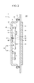
- FIG. 2 is a cross-sectional view taken along line - of FIG. 1 .
- the scan board 250 includes a scan integrated circuit (IC) generating a high frequency scan pulse to be applied to the scan electrode.
- the scan IC is an example of the switch 60 in accordance with the present embodiment.
- the scan board 250 is disposed between the chassis base 20 and the heat dissipating plate 40, and is fixed to a plurality of bosses 18 by screws 19.
- the plurality of bosses 18 are formed on the inner surface of the heat dissipating plate 40.
- the scan board 250 is generally parallel to the heat dissipating plate 40 and the chassis base 20.
- the switch 60 is electrically connected to the scan board 250 and fixed to a plane portion 42 of the heat dissipating plate 40.
- the heat dissipating plate 40 has an installation hole 41 facing the switch 60 to allow a fastener to fasten the switch to the heat dissipating plate.
- the scan board 250 may have a double-sided circuit pattern structure including a first circuit pattern 51 that faces the chassis base 20 and a second circuit pattern 52 that faces the heat dissipating plate 40.
- the switch 60 is connected to the second circuit pattern 52.
- the switch 60 may be a dual in-line package (DIP) type and may be connected to the second circuit pattern 52.
- DIP dual in-line package
- the switch 60 is mechanically installed to the heat dissipating plate 40 and is electrically connected to the second circuit pattern 52 of the heat dissipating plate 40. In this instance, the switch 60 contacts the inner surface of the heat dissipating plate 40.
- the switch 60 attached to the heat dissipating plate 40 may quickly transfer the intense heat generated by the switch 60 during operation to the heat dissipating plate 40.
- the heat dissipating plate 40 functions as a heat sink for the switch 60. Accordingly, the heat dissipation performance of the switch 60 may be improved.
- a thermal grease may be further provided between the switch 60 and the inner surface of the heat dissipating plate 40. In this case, due to a heat transfer function of the thermal grease, the heat dissipation performance of the switch 60 is further improved.
- a separate and additional heat sink is not provided for the heat dissipation of the switch 60. Therefore, as compared to when an additional and separate heat sink is provided, it is possible to minimize a thickness (z-axis direction distance) of the plasma display device 100.
- the scan board 250 has a penetration hole 54 facing and aligned with the installation hole 41 of the heat dissipating plate 40 such that the switch 60 may be attached to the heat dissipating plate 40 while being covered by the scan board 250.
- a driver (not shown) is inserted into the penetration hole 54 of the scan board 250, the screw 19 is inserted into the switch 60 and then screwed into the installation hole 41 of the heat dissipating plate 40. Accordingly, the switch 60 is fastened to the heat dissipating plate 40.
- the scan board 250 is mounted to the boss 18 formed in the heat dissipating plate 40. Accordingly, the scan board 250 is mounted to the heat dissipating plate 40.
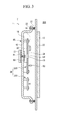
- FIG. 3 is a cross-sectional view of a plasma display device 200 according to a second embodiment of the present invention
- FIG. 4 is a partial exploded perspective view of a printed circuit board, a switch, and a heat sink shown in FIG. 3 .
- the plasma display device 200 according to the second embodiment further includes a heat sink 72.
- a switch 60 is installed on the inner surface of a heat dissipating plate 40 through an installation hole 41 and a screw 19.
- the heat sink 72 is installed on the outer surface of the heat dissipating plate 40, corresponding to the switch 60.
- the heat sink 72 may protrude in the z-axis direction within a suitable range of space between the heat dissipating plate 40 and a back cover (not shown). Specifically, the heat sink 72 may be provided on the outer surface of the heat dissipating plate 40 within a range such that it protrudes without increasing the overall thickness (z-axis direction) of the plasma display device 200.
- the heat sink may include fins. With respect to thermal conductivity, the heat sink 72 dissipates more heat than the heat dissipating plate 40 alone. Thus, the intense heat generated by the switch 60 is more quickly dissipated through the heat sink 72 and a portion of the heat dissipating plate 40 corresponding to the switch 60.
- the second embodiment may increase the thickness (z-axis direction) of the plasma display device 200 due to the heat sink 72.
- it is possible to more quickly dissipate the heat generated by the switch 60 via the heat sink 72, and therefore, it is possible to prevent the heat from spreading over the heat dissipating plate 40.
- FIG. 5 is a cross-sectional view of a plasma display device 300 according to the third embodiment of the present invention.
- the plasma display device 300 includes a switch 60 and a heat sink 372 in different locations from previously described embodiments.
- the heat dissipating plate 40 includes a plane portion 42, a side portion 43, and a flange 44 forming a 3-dimensional space for accommodating printed circuit boards 50, for example, a scan board 250.
- the plane portion 42 is formed at the rear of the scan board 250 and is generally parallel to the scan board 250 and a chassis base 20. Specifically, the plane portion 42 defines the rearmost part of the heat dissipating plate 40.
- the side portion 43 is curved from the plane portion 42 toward the chassis base 20. Specifically, the side portion 43 defines the side of the heat dissipating plate 40 and is generally perpendicular to the plane portion 42.
- the flange 44 is curved from the side portion 430 and parallel with the plane portion 42 generally corresponding to the outer edge of the chassis base 20.
- the flange 44 is installed on the chassis base 20 to define the front of the heat dissipating plate 40.
- the switch 60 may be installed on the inner surface of the side portion 43 and the heat sink 372 may be installed on the outer surface of the side portion 43 generally opposite the switch.
- the switch 60 and the heat sink 372 are both installed on the side portion 43 of the heat dissipating plate 40. Therefore, it is possible to provide a structure that may further improve heat dissipation performance of the switch 60 and yet will not increase a thickness (z-axis direction thickness) of the plasma display device 300.
- FIG. 6 is a cross-sectional view of a plasma display device 400 according to the fourth embodiment of the present invention.
- the plasma display device 400 generally corresponds to the plasma display device 200 according to the second embodiment.
- a switch 60 is installed on the inner surface of a heat dissipating plate 40 via an installation hole 41 and a screw 19 and a heat sink 472 is installed on the switch 60. Specifically, the switch 60 is disposed between the inner surface of the heat dissipating plate 40 and the heat sink 472.
- the heat sink 472 improves the heat dissipating performance of the switch 60, but does not protrude externally from the heat dissipating plate 40. Therefore, compared to the second embodiment, the thickness (z-axis direction thickness) of the plasma display device 400 is not increased.
- a single heat dissipating plate 40 generally corresponds to the single chassis base 20 to thereby integrally cover all the printed circuit boards 50. However, although not illustrated, the heat dissipating plate 40 may be formed to cover each of the printed circuit boards 50 individually.
Applications Claiming Priority (1)
| Application Number | Priority Date | Filing Date | Title |
|---|---|---|---|
| KR1020080049192A KR20090123221A (ko) | 2008-05-27 | 2008-05-27 | 플라즈마 디스플레이 장치 |
Publications (1)
| Publication Number | Publication Date |
|---|---|
| EP2129205A1 true EP2129205A1 (en) | 2009-12-02 |
Family
ID=40908579
Family Applications (1)
| Application Number | Title | Priority Date | Filing Date |
|---|---|---|---|
| EP09157685A Withdrawn EP2129205A1 (en) | 2008-05-27 | 2009-04-09 | Plasma display device |
Country Status (5)
| Country | Link |
|---|---|
| US (1) | US20090296353A1 (ko) |
| EP (1) | EP2129205A1 (ko) |
| JP (1) | JP2009288764A (ko) |
| KR (1) | KR20090123221A (ko) |
| CN (1) | CN101593467A (ko) |
Families Citing this family (5)
| Publication number | Priority date | Publication date | Assignee | Title |
|---|---|---|---|---|
| KR102377472B1 (ko) | 2015-03-10 | 2022-03-23 | 삼성전자주식회사 | 반도체 패키지 및 그 제조방법 |
| CN105163563B (zh) * | 2015-08-27 | 2018-04-17 | 苏州佳世达电通有限公司 | 显示装置 |
| US9659466B1 (en) * | 2016-03-04 | 2017-05-23 | Penetek Technology, Inc. | POS apparatus and display device |
| JP6535058B2 (ja) * | 2017-08-10 | 2019-06-26 | シャープ株式会社 | 表示装置及びテレビジョン受信機 |
| CN110459136B (zh) * | 2019-08-29 | 2021-08-20 | 上海天马微电子有限公司 | 一种显示面板及显示装置 |
Citations (5)
| Publication number | Priority date | Publication date | Assignee | Title |
|---|---|---|---|---|
| US4631819A (en) * | 1985-05-29 | 1986-12-30 | Motorola, Inc. | Low stress, tolerance free method for mounting power devices |
| US20020014840A1 (en) * | 2000-06-19 | 2002-02-07 | Pioneer Corporation | Heat-dissipation structure of plasma display panel device |
| US20050259401A1 (en) * | 2004-05-18 | 2005-11-24 | Chan-Young Han | Plasma display device |
| US20060077619A1 (en) * | 2004-10-11 | 2006-04-13 | Ki-Jung Kim | Plasma display device |
| US20060181853A1 (en) * | 2005-02-16 | 2006-08-17 | Kwang-Jin Jeong | Plasma display device |
Family Cites Families (5)
| Publication number | Priority date | Publication date | Assignee | Title |
|---|---|---|---|---|
| JPH11284936A (ja) * | 1998-03-31 | 1999-10-15 | Fujitsu General Ltd | プラズマディスプレイ装置 |
| JP3659810B2 (ja) * | 1998-08-05 | 2005-06-15 | パイオニア株式会社 | 二次元表示装置の駆動モジュール取付構造 |
| KR100612276B1 (ko) * | 2004-04-29 | 2006-08-11 | 삼성에스디아이 주식회사 | 플라즈마 디스플레이 장치 |
| KR100717799B1 (ko) * | 2005-10-18 | 2007-05-11 | 삼성에스디아이 주식회사 | 플라즈마 디스플레이 장치 |
| KR100829754B1 (ko) * | 2007-03-02 | 2008-05-15 | 삼성에스디아이 주식회사 | 섀시 베이스와 회로기판의 체결구조 및 이를 구비한디스플레이 장치 |
-
2008
- 2008-05-27 KR KR1020080049192A patent/KR20090123221A/ko not_active Application Discontinuation
- 2008-10-21 JP JP2008271260A patent/JP2009288764A/ja not_active Withdrawn
-
2009
- 2009-03-24 US US12/410,087 patent/US20090296353A1/en not_active Abandoned
- 2009-04-09 EP EP09157685A patent/EP2129205A1/en not_active Withdrawn
- 2009-04-13 CN CNA200910132035XA patent/CN101593467A/zh active Pending
Patent Citations (5)
| Publication number | Priority date | Publication date | Assignee | Title |
|---|---|---|---|---|
| US4631819A (en) * | 1985-05-29 | 1986-12-30 | Motorola, Inc. | Low stress, tolerance free method for mounting power devices |
| US20020014840A1 (en) * | 2000-06-19 | 2002-02-07 | Pioneer Corporation | Heat-dissipation structure of plasma display panel device |
| US20050259401A1 (en) * | 2004-05-18 | 2005-11-24 | Chan-Young Han | Plasma display device |
| US20060077619A1 (en) * | 2004-10-11 | 2006-04-13 | Ki-Jung Kim | Plasma display device |
| US20060181853A1 (en) * | 2005-02-16 | 2006-08-17 | Kwang-Jin Jeong | Plasma display device |
Also Published As
| Publication number | Publication date |
|---|---|
| KR20090123221A (ko) | 2009-12-02 |
| CN101593467A (zh) | 2009-12-02 |
| JP2009288764A (ja) | 2009-12-10 |
| US20090296353A1 (en) | 2009-12-03 |
Similar Documents
| Publication | Publication Date | Title |
|---|---|---|
| US7468887B2 (en) | Plasma display device | |
| US7447034B2 (en) | Chassis base assembly and flat panel display device having the same | |
| EP1993336A2 (en) | Chassis base assembly and display device including the same | |
| US7372700B2 (en) | Plasma display device | |
| US7619891B2 (en) | Plasma display apparatus | |
| KR100696832B1 (ko) | 플라즈마 디스플레이 모듈 | |
| JP2006113538A (ja) | プラズマディスプレイ装置 | |
| US20090096952A1 (en) | Printed circuit board assembly and plasma display apparatus including the same | |
| EP2129205A1 (en) | Plasma display device | |
| KR20040095854A (ko) | 플라즈마 디스플레이 패널을 채용한 화상 표시장치 | |
| US8040679B2 (en) | Plasma display apparatus having segmented chassis base | |
| KR20050045141A (ko) | 플라즈마 디스플레이 장치 | |
| KR100667932B1 (ko) | 플라즈마 디스플레이 장치 | |
| US7443681B2 (en) | Heat dissipator for display apparatus and plasma display apparatus including the heat dissipator | |
| KR100612348B1 (ko) | 플라즈마 디스플레이 장치 | |
| KR20060069569A (ko) | 플라즈마 디스플레이 장치 | |
| KR20040036080A (ko) | Pdp 회로기판용 커버 | |
| KR100626053B1 (ko) | 플라즈마 디스플레이 모듈 | |
| KR20060109649A (ko) | 플라즈마 디스플레이 장치 | |
| KR100696493B1 (ko) | 플라즈마 디스플레이 장치 | |
| KR100749461B1 (ko) | 플라즈마 디스플레이 장치 | |
| KR20070056629A (ko) | 플라즈마 디스플레이 장치 | |
| KR20080038636A (ko) | 플라즈마 디스플레이 장치 | |
| KR20060087764A (ko) | 플라즈마 디스플레이 장치 | |
| KR20080037795A (ko) | 플라즈마 디스플레이 장치 |
Legal Events
| Date | Code | Title | Description |
|---|---|---|---|
| PUAI | Public reference made under article 153(3) epc to a published international application that has entered the european phase |
Free format text: ORIGINAL CODE: 0009012 |
|
| 17P | Request for examination filed |
Effective date: 20090409 |
|
| AK | Designated contracting states |
Kind code of ref document: A1 Designated state(s): AT BE BG CH CY CZ DE DK EE ES FI FR GB GR HR HU IE IS IT LI LT LU LV MC MK MT NL NO PL PT RO SE SI SK TR |
|
| GRAP | Despatch of communication of intention to grant a patent |
Free format text: ORIGINAL CODE: EPIDOSNIGR1 |
|
| STAA | Information on the status of an ep patent application or granted ep patent |
Free format text: STATUS: THE APPLICATION IS DEEMED TO BE WITHDRAWN |
|
| 18D | Application deemed to be withdrawn |
Effective date: 20100720 |