EP2129107A1 - Solid-state imaging apparatus - Google Patents
Solid-state imaging apparatus Download PDFInfo
- Publication number
- EP2129107A1 EP2129107A1 EP07737541A EP07737541A EP2129107A1 EP 2129107 A1 EP2129107 A1 EP 2129107A1 EP 07737541 A EP07737541 A EP 07737541A EP 07737541 A EP07737541 A EP 07737541A EP 2129107 A1 EP2129107 A1 EP 2129107A1
- Authority
- EP
- European Patent Office
- Prior art keywords
- circuit
- output
- transimpedance
- capacitor
- holding
- Prior art date
- Legal status (The legal status is an assumption and is not a legal conclusion. Google has not performed a legal analysis and makes no representation as to the accuracy of the status listed.)
- Granted
Links
Images

Classifications
-
- H—ELECTRICITY
- H04—ELECTRIC COMMUNICATION TECHNIQUE
- H04N—PICTORIAL COMMUNICATION, e.g. TELEVISION
- H04N25/00—Circuitry of solid-state image sensors [SSIS]; Control thereof
- H04N25/70—SSIS architectures; Circuits associated therewith
- H04N25/76—Addressed sensors, e.g. MOS or CMOS sensors
- H04N25/77—Pixel circuitry, e.g. memories, A/D converters, pixel amplifiers, shared circuits or shared components
- H04N25/771—Pixel circuitry, e.g. memories, A/D converters, pixel amplifiers, shared circuits or shared components comprising storage means other than floating diffusion
-
- H—ELECTRICITY
- H10—SEMICONDUCTOR DEVICES; ELECTRIC SOLID-STATE DEVICES NOT OTHERWISE PROVIDED FOR
- H10F—INORGANIC SEMICONDUCTOR DEVICES SENSITIVE TO INFRARED RADIATION, LIGHT, ELECTROMAGNETIC RADIATION OF SHORTER WAVELENGTH OR CORPUSCULAR RADIATION
- H10F39/00—Integrated devices, or assemblies of multiple devices, comprising at least one element covered by group H10F30/00, e.g. radiation detectors comprising photodiode arrays
- H10F39/10—Integrated devices
- H10F39/12—Image sensors
- H10F39/18—Complementary metal-oxide-semiconductor [CMOS] image sensors; Photodiode array image sensors
Definitions
- the present invention relates to a solid-state imaging device.
- a solid-state imaging device including a plurality of pixel sections each including a photodiode which generates charges corresponding to the intensity of incident light, and a signal processing circuit which outputs voltages corresponding to the amount of charges successively output to a common wire from the plurality of pixel sections.
- the solid-state imaging device including the plurality of pixel sections one-dimensionally aligned can handle a larger charge quantity that a CCD cannot handle, and the length in the alignment direction of the plurality of pixel sections can be increased to, for example, 500 ⁇ m to 2mm, and therefore, the solid-state imaging device is used as a one-dimensional image sensor in spectrometers, displacement meters, and barcode readers, etc.
- the common wire connecting the plurality of pixel sections and the signal processing circuit to each other is long, so that the capacity of the common wire is high.
- the junction capacitances of the photodiodes included in the plurality of pixel sections, respectively, are also high. Therefore, in this solid-state imaging device, it is difficult to increase the imaging speed.
- a solid-state imaging device having an increased imaging speed (refer to, for example, Non-Patent Document 1).
- the plurality of pixel sections include, respectively, photoelectric converting circuits which include photodiodes for generating charges corresponding to the intensity of incident light and output voltages corresponding to the amount of the generated charges, and holding circuits which hold the voltages output from the photoelectric converting circuits and successively output the amount of charges corresponding to the held voltages to the common wire.
- junction capacitances of the photodiodes included in the plurality of pixel sections, respectively can be made smaller as viewed from the signal processing circuit, and the imaging speed can be increased.
- Non-Patent Document 1 K. Hara, et al., "A Linear Logarithmic CMOS Sensor with Offset Calibration Using an Injected Charge Signal," ISSCC 2005 Dig. Tech. Papers, pp. 354-355 (2005 )
- the present invention was made to solve the above-described problem, and an object thereof is to provide a solid-state imaging device which can realize an increase in imaging speed and an increase in imaging sensitivity simultaneously.
- a solid-state imaging device of the present invention includes:
- this solid-state imaging device in the pixel sections, charges are generated in response to the incidence of the light on the photodiodes, and voltages corresponding to the amounts of the generated charges are output from the photoelectric converting circuits.
- the voltages output from the photoelectric converting circuits are held by the holding circuits, and charge quantities corresponding to the held voltages are successively output from the holding circuits to the common wire.
- Charges output from the holding circuits of the pixel sections are input into the transimpedance circuit through the common wire, and a pulse current having a pulse height corresponding to the input charge quantity is output from the transimpedance circuit.
- the current output from the transimpedance circuit is input into the integrating circuit, and a voltage corresponding to the input current is output from the integrating circuit.
- each of the plurality of pixel sections includes a first holding circuit and a second holding circuit as a holding circuit
- the solid-state imaging device further includes (2) a first common wire connected to the first holding circuit and a second common wire connected to the second holding circuit as the common wire; (3) a first transimpedance circuit connected to the first common wire and a second transimpedance circuit connected to the second common wire as the transimpedance circuit; (4) a first integrating circuit connected to the first transimpedance circuit and a second integrating circuit connected to the second transimpedance circuit as the integrating circuit; and (5) a difference arithmetic circuit which inputs voltages output from the first integrating circuit and the second integrating circuits, respectively, and outputs a voltage corresponding to a difference between the input two voltages.
- a voltage held by the first holding circuit of each pixel section is input into the difference arithmetic circuit through the first common wire, the first transimpedance circuit, and the first integrating circuit.
- the voltage held by the second holding circuit of each pixel section is input into the difference arithmetic circuit through the second common wire, the second transimpedance circuit, and the second integrating circuit. Then, a voltage corresponding to a difference between voltages output from the first integrating circuit and the second integrating circuit, respectively, is output from the difference arithmetic circuit.
- the voltage held by the first holding circuit is a noise component
- the voltage held by the second holding circuit is a signal component
- the noise component is superimposed on the signal component
- the voltage to be output from each difference arithmetic circuit is only a signal component from which the noise component was removed. It is known that, in the charge amplifier circuit, the output voltage fluctuates after a reset operation is finished and the reset switch is opened, and this is called a reset noise.
- the reset noise generated in the photoelectric converting circuit is removed by the two holding circuits described above.
- the capacity of a capacitor for holding a voltage in the holding circuit is in the range of 1pF to 2pF, and the capacity of the first capacitor of the transimpedance circuit is in the range of 1pF to 5pF (more preferably, 1pF to 3pF). This case is preferable particularly to increasing the imaging speed and imaging sensitivity.
- the present invention can realize an increase in imaging speed and an increase in imaging sensitivity simultaneously.
- Fig. 1 is a configuration view of a solid-state imaging device 1 of the present embodiment.
- the solid-state imaging device 1 shown in this drawing includes N pixel sections 101 to 10 N , a first transimpedance circuit 20a, a second transimpedance circuit 20b, a first integrating circuit 30a, a second integrating circuit 30b, a difference arithmetic circuit 40, and a Controlling section 90.
- N is an integer not less than 2
- n appearing hereinafter is an integer not less than 1 and not more than N.
- the N pixel sections 10 1 to 10 N have a common configuration, and are one-dimensionally aligned, and include photodiodes which generate charges, the amounts of the generated charges corresponding to the intensities of the incident light.
- Each pixel section 10 n has two output terminals, and one output terminal is connected to a first common wire 50a, and the other output terminal is connected to a second common wire 50b.
- the transimpedance circuit 20a and the transimpedance circuit 20b have a common configuration. An input terminal of the transimpedance circuit 20a is connected to the common wire 50a. An input terminal of the transimpedance circuit 20b is connected to the common wire 50b.
- the integrating circuit 30a and the integrating circuit 30b have a common configuration.
- An input terminal of the integrating circuit 30a is connected to an output terminal of the transimpedance circuit 20a via a resistor 60a.
- An input terminal of the integrating circuit 30b is connected to an output terminal of the transimpedance circuit 20b via a resistor 60b.
- the difference arithmetic circuit 40 has two input terminals, and one input terminal is connected to an output terminal of the integrating circuit 30a, and the other input terminal is connected to an output terminal of the integrating circuit 30b.
- the difference arithmetic circuit 40 inputs voltages output from the integrating circuit 30a and the integrating circuit 30b, respectively, and outputs a voltage corresponding to a difference between these two input voltages.
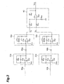
- Fig. 2 is a circuit diagram of each pixel section 10 n included in the solid-state imaging device 1 of the present embodiment.
- Each pixel section 10 n includes a photoelectric converting circuit 11, a first holding circuit 12a, and a second holding circuit 12b.
- the holding circuit 12a and the holding circuit 12b have a common configuration.
- the photoelectric converting circuit 11 is of a PPS (Passive Pixel Sensor) type, and includes a photodiode PD which generates charge quantities corresponding to an incident light amount, an integrating circuit 13 which outputs a voltage corresponding to the generated charge quantity, and a switch SW 11 provided between the photodiode PD and the integrating circuit 13.
- the integrating circuit 13 includes an amplifier A 13 , a capacitor C 13 , and a switch SW 13 .
- An anode terminal of the photodiode PD is grounded, and a cathode terminal of the photodiode PD is connected to the switch SW 11 .
- An inverting input terminal of the amplifier A 13 included in the integrating circuit 13 is connected to the cathode terminal of the photodiode PD via the switch SW 11 .
- a fixed reference voltage Vref is input into a non-inverting input terminal of the amplifier A 13 included in the integrating circuit 13.
- the capacitor C 13 and the switch SW 13 are connected in parallel to each other, and provided between the inverting input terminal and the output terminal of the amplifier A 13 .
- the capacitor C 13 is discharged, and a voltage to be output from the integrating circuit 13 is initialized.
- the switch SW 13 opens and the switch Sw 11 closes, charges accumulated in the junction capacitance section of the photodiode PD in response to light incidence on this photodiode PD are input into the integrating circuit 13 through the switch SW l1 , and accumulated in the capacitor C 13 .
- a voltage corresponding to a charge quantity accumulated in the capacitor C 13 is output from the integrating circuit 13.
- Each of the holding circuits 12a and 12b holds a voltage output from the photoelectric converting circuit 11 and outputs a charge quantity corresponding to the held voltage to the common wire, and includes a capacitor C 12 , a switch SW 1 , and a switch SW 2 .
- a capacitor C 12 In each of the holding circuits 12a and 12b, one end of the capacitor C 12 is grounded, and the other end of the capacitor C 12 is connected to the output terminal of the amplifier A 13 of the integrating circuit 13 via the switch SW 1 .
- the holding circuit 12a the other end of the capacitor C 12 is connected to the common wire 50a via the switch SW 2 .
- the holding circuit 12b the other end of the capacitor C 12 is connected to the common wire 50b via the switch SW 2 .
- holding circuits 12a and 12b when the switch SW 1 opens, a voltage output from the photoelectric converting circuit 11 before opening of the switch SW 1 is held by the capacitor C 12 . Then, when the switch SW 2 closes, a charge quantity corresponding to the voltage held by the capacitor C 12 is output to the common wire 50a, 50b.
- the holding circuits 12a and 12b operate at different timings from each other. In other words, one holding circuit 12a holds an initial voltage (noise component) output from the integrating circuit 13 immediately after (at the time t1) the switch SW 13 opens from a closed state in the integrating circuit 13 included in the photoelectric converting circuit 11.
- the switch SW 11 connected to the photodiode PD is opened at the time of acquisition of the initial voltage, a noise component in the integrating circuit 13 is held, and if the switch SW 11 is closed, a noise component caused by background light, etc., made incident on the photodiode PD is also held in addition to the noise component in the integrating circuit 13.
- the switch SW 1 is closed while the switch SW 2 of the holding circuit 12a is left open, however, thereafter, the switch SW 1 also opens quickly (time t2), and charges are held in the capacitor C 12 of the holding circuit 12a.
- the switch SW 1 is closed (time t3) while the switch SW 2 of the holding circuit 12b is left open, and charges are accumulated in the capacitor C 12 of the holding circuit 12b.
- the other holding circuit 12b holds a voltage (signal component) which is output from the integrating circuit 13 while charges generated in the photodiode PD in response to light incidence are accumulated in the capacitor C 13 of the integrating circuit 13.
- a noise component caused by background light, etc., made incident on the photodiode PD is superimposed in addition to the noise component in the integrating circuit 13.
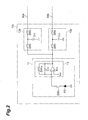
- Fig. 3 is a circuit diagram of transimpedance circuits 20a and 20b, integrating circuits 30a and 30b, and a difference arithmetic circuit 40 included in the solid-state imaging device 1 of the present embodiment.
- Each of the transimpedance circuits 20a and 20b includes an amplifier A 20 , a capacitor C 20 , and a resistor R 20 .
- An inverting input terminal of the amplifier A 20 of the transimpedance circuit 20a is connected to the common wire 50a.
- An inverting input terminal of the amplifier A 20 of the transimpedance circuit 20b is connected to the common wire 50b.
- a fixed reference voltage Vref is input into a non-inverting input terminal of the amplifier A 20 .
- the capacitor C 20 and the resistor R 20 are connected in parallel to each other, and provided between the inverting input terminal and the output terminal of the amplifier A 20 .
- one transimpedance circuit 20a when the switch SW 2 of the holding circuit 12a included in the pixel section 10 n closes (time t4), a charge quantity corresponding to a voltage held by the capacitor C 12 of the holding circuit 12a is input through the common wire 50a, and a pulse current having a pulse height corresponding to the input charge quantity is output to the integrating circuit 30a.
- the switch SW 2 of the holding circuit 12b included in the pixel section 10 n closes (time t4)
- a charge quantity corresponding to the voltage held by the capacitor C 12 of the holding circuit 12b is input through the common wire 50b, and a pulse current having a pulse height corresponding to the input charge quantity is output to the integrating circuit 30b.
- Each of the integrating circuits 30a and 30b includes an amplifier A 30 , a capacitor C 30 , and a switch SW 30 .
- An inverting input terminal of the amplifier A 30 of the integrating circuit 30a is connected to the output terminal of the transimpedance circuit 20a via a resistor 60a.
- An inverting input terminal of the amplifier A 30 of the integrating circuit 30b is connected to the output terminal of the transimpedance circuit 20b via a resistor 60b.
- a fixed reference voltage Vref is input into a non-inverting input terminal of the amplifier A 30 .
- the capacitor C 30 and the switch SW 30 are connected in parallel to each other, and provided between the inverting input terminal and the output terminal of the amplifier A 30 .
- each of the integrating circuits 30a and 30b when the switch SW 30 closes, the capacitor C 30 is discharged, and a voltage to be output from the integrating circuit 30a, 30b is initialized.
- the switch SW 30 when the switch SW 30 opens, a current output from the transimpedance circuit 20a is input through the resistor 60a, and a charge quantity corresponding to the input current is accumulated in the capacitor C 30 , and a voltage corresponding to the charge quantity accumulated in the capacitor C 30 is output from the integrating circuit 30a.
- the switches SW 30 may be opened, and before this input, the switches SW 30 are closed once and the capacitors C 30 are respectively reset.
- the switch SW 30 is used, and it is also possible to use a resistor, however, when a resistor is used, charges which were integrated and accumulated in the capacitor C 30 are discharged by the resistor, and the voltage to be output from the integrating circuit 30b becomes smaller with time. As in the case of the present embodiment, by using a switch, charges accumulated in the capacitor are not discharged, and accordingly, a gain to be secured becomes higher.
- the difference arithmetic circuit 40 includes an amplifier A 40 and resistors R 41 to R 44 .
- An inverting input terminal of the amplifier A 40 is connected to the output terminal of the integrating circuit 30a via the resistor R 41 , and connected to the output terminal of the amplifier A 40 via the resistor R 42 .
- a non-inverting input terminal of the amplifier A 40 is connected to the output terminal of the integrating circuit 30b via the resistor R 43 , and grounded via the resistor R 44 .
- a voltage Vout to be output from the output terminal of the amplifier A 40 is expressed in the following equation (1).
- the voltage Vout to be output from the difference arithmetic circuit 40 is a product obtained by multiplying a difference between the output voltage Va of the integrating circuit 30a and the output voltage Vb of the integrating circuit 30b (Vb-Va) by a gain (R 2 /R 1 ).
- V ⁇ o ⁇ u ⁇ t ⁇ V ⁇ b ⁇ V ⁇ a ⁇ R 2 / R 1
- the Controlling section 90 outputs signals for controlling the opening and closing operations of the switch SW 11 and the switch SW 13 included in the photoelectric converting circuit 11 of each pixel section 10 n , outputs signals for controlling the opening and closing operations of the switch SW 1 and the switch SW 2 included in the holding circuit 12a and the holding circuit 12b of each pixel section 10 n , and outputs signals for controlling the opening and closing operations of the switches SW30 included in the integrating circuit 30a and the integrating circuit 30b, respectively.
- the solid-state imaging device 1 of the present embodiment operates based on control signals output from the Controlling section 90.
- An example of an operation of the solid-state imaging device 1 of the present embodiment is as follows.
- the operation example described hereinafter is based on control signals output from the Controlling section 90.
- the switch SW 13 of the integrating circuit 13 closes, the capacitor C 13 is discharged, and a voltage to be output from the photoelectric converting circuit 11 is initialized. Further, at the moment that the switch SW 13 of the integrating circuit 13 opens, an integration-enabled state is obtained, and an initial voltage containing noise is generated from the interacting circuit 13. Thereafter, the switch SW 1 of the holding circuit 12a opens and closes, and accordingly, the initial voltage (noise component) output from the photoelectric converting circuit 11 at this time is held by the capacitor C 12 of the holding circuit 12a.
- a charge quantity corresponding to the voltage (noise component) held by the holding circuit 12a during the predetermined period in which the switch SW 2 of the holding circuit 12a of the pixel section 10 n closes is input into the transimpedance circuit 20a through the common wire 50a, and a pulse current having a pulse height corresponding to the input charge quantity is output from the transimpedance circuit 20a.
- the pulse current output from the transimpedance circuit 20a is input into the integrating circuit 30a through the resistor 60a. Then, a charge quantity corresponding to the input current is accumulated in the capacitor C 30 of the integrating circuit 30a, and a voltage (noise component) Va corresponding to the charge quantity accumulated in the capacitor C 30 is output from the integrating circuit 30a.
- a charge quantity corresponding to the voltage (signal component + noise component) held by the holding circuit 12b during the predetermined period in which the switch SW 2 of the holding circuit 12b of the pixel section 10 n closes is input into the transimpedance circuit 20b through the common wire 50b, and a pulse current having a pulse height corresponding to the input charge quantity is output from the transimpedance circuit 20b.
- the pulse current output from the transimpedance circuit 20b is input into the integrating circuit 30b through the resistor 60b.
- a charge quantity corresponding to the input current is accumulated in the capacitor C 30 of the integrating circuit 30b, and a voltage (signal component + noise component) Vb corresponding to the charge quantity accumulated in the capacitor C 30 is output from the integrating circuit 30b.
- the voltage (noise component) Va output from the integrating circuit 30a and the voltage (signal component + noise component) Vb output from the integrating circuit 30b are input into the difference arithmetic circuit 40. Then, a voltage Vout expressed in equation (1) described above is output from the difference arithmetic circuit 40.
- a voltage corresponding to a charge quantity generated in the photodiode PD is output from the photoelectric converting circuit 11, and this voltage is held by the holding circuits 12a and 12b. Therefore, even if the junction capacitance of the photodiode PD included in each pixel section 10 n is high, the imaging speed is prevented from deteriorating.
- the common wire 50a between the holding circuits 12a of the pixel sections 10 n and the transimpedance circuit 20a is connected to the inverting input terminal of the amplifier A 20 included in the transimpedance circuit 20a, and is maintained at the same fixed voltage as the voltage Vref input into the non-inverting input terminal of the amplifier A 20 being imaginarily short-circuited to the inverting input terminal.
- the common wire 50b between the holding circuits 12b of the pixel sections 10 n and the transimpedance circuit 20b is also maintained at the fixed voltage.
- the voltage Vout to be output from the difference arithmetic circuit 40 is a product obtained by multiplying a difference (Vb-Va) between the output voltage (noise component) Va of the integrating circuit 30a and the output voltage (signal component + noise component) Vb of the integrating circuit 30b by the gain (R 2 /R 1 ).
- This difference (Vb-Va) corresponds to a difference between the voltages held by the holding circuits 12a and 12b, respectively. Therefore, the voltage Vout to be output from the difference arithmetic circuit 40 becomes highly accurate because a noise component such as an offset, reset noise, and background light, etc., contained in the output voltage of the integrating circuit 13 is removed.
- the transimpedance circuits 20a and 20b have wide bandwidths, so that a thermal noise component is easily superimposed on their output signals.
- high-frequency components of the output signals from the transimpedance circuits 20a and 20b are cut-off by the integrating circuits 30a and 30b, so that output signals from the integrating circuits 30a and 30b have reduced thermal noise components.
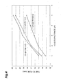
- Fig. 4 is a graph showing a relationship between the capacity (hold capacitance) C h of the capacitor C 12 included in each of the holding circuits 12a and 12b of each pixel section 10 n , and a time to peak of a pulse signal output from the transimpedance circuit 20a, 20b.
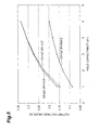
- Fig. 5 is a graph showing a relationship between a capacity (hold capacitance) C h of the capacitor C 12 included in each of the holding circuits 12a and 12b of each pixel section 10 n , and a pulse height (output voltage value) of a pulse signal output from the transimpedance circuit 20a, 20b.
- the capacity C h of the capacitor C 12 included in each of the holding circuits 12a and 12b of each pixel section 10 n is in the range of 1pF to 2pF
- the capacity C f of the capacitor C 20 included in each of the transimpedance circuits 20a and 20b is in the range of 1pF to 5pF (more preferably, 1pF to 3pF). In these ranges, the imaging speed and imaging sensitivity can be increased higher than other cases.
- the photoelectric converting circuit 11 included in each pixel section 10 n is of a PPS type in the embodiment described above, however, an APS (Active Pixel Sensor) type may also be used.
Landscapes
- Engineering & Computer Science (AREA)
- Multimedia (AREA)
- Signal Processing (AREA)
- Transforming Light Signals Into Electric Signals (AREA)
Abstract
Description
- The present invention relates to a solid-state imaging device.
- There is known a solid-state imaging device including a plurality of pixel sections each including a photodiode which generates charges corresponding to the intensity of incident light, and a signal processing circuit which outputs voltages corresponding to the amount of charges successively output to a common wire from the plurality of pixel sections. The solid-state imaging device including the plurality of pixel sections one-dimensionally aligned can handle a larger charge quantity that a CCD cannot handle, and the length in the alignment direction of the plurality of pixel sections can be increased to, for example, 500µm to 2mm, and therefore, the solid-state imaging device is used as a one-dimensional image sensor in spectrometers, displacement meters, and barcode readers, etc.
- In the solid-state imaging device thus configured, the common wire connecting the plurality of pixel sections and the signal processing circuit to each other is long, so that the capacity of the common wire is high. The junction capacitances of the photodiodes included in the plurality of pixel sections, respectively, are also high. Therefore, in this solid-state imaging device, it is difficult to increase the imaging speed. On the other hand, there is known a solid-state imaging device having an increased imaging speed (refer to, for example, Non-Patent Document 1).
- In the solid-state imaging device described in
Non-Patent Document 1, the plurality of pixel sections include, respectively, photoelectric converting circuits which include photodiodes for generating charges corresponding to the intensity of incident light and output voltages corresponding to the amount of the generated charges, and holding circuits which hold the voltages output from the photoelectric converting circuits and successively output the amount of charges corresponding to the held voltages to the common wire. With this configuration, junction capacitances of the photodiodes included in the plurality of pixel sections, respectively, can be made smaller as viewed from the signal processing circuit, and the imaging speed can be increased.
Non-Patent Document 1: K. Hara, et al., "A Linear Logarithmic CMOS Sensor with Offset Calibration Using an Injected Charge Signal," ISSCC 2005 Dig. Tech. Papers, pp. 354-355 (2005) - However, even in the solid-state imaging device configured as described in Non-Patent
Document 1 described above, if the number of pixels increases, the common wire accordingly lengthens and the wiring capacity increases. When charges are transferred from the holding circuits of the plurality of pixel sections, respectively, to the signal processing circuit through the common wire, charge distribution occurs among the capacities of the holding circuits and the wiring capacity, and the voltage at the input terminal of the signal processing circuit decreases. To compensate for this voltage decrease at the input terminal, the gain of the signal processing circuit may be increased, however, in this case, the processing speed of the signal processing circuit is reduced. In other words, even in the solid-state imaging device configured as described in Non-PatentDocument 1, it is difficult to realize an increase in imaging speed and an increase in imaging sensitivity simultaneously. - The present invention was made to solve the above-described problem, and an object thereof is to provide a solid-state imaging device which can realize an increase in imaging speed and an increase in imaging sensitivity simultaneously.
- A solid-state imaging device of the present invention includes:
- (1) a plurality of pixel sections including, respectively, photoelectric converting circuits which include photodiodes for generating charges corresponding to intensities of incident lights and output voltages corresponding to the amounts of the generated charges, and holding circuits which hold voltages output from the photoelectric converting circuits and successively output the charges to a common wire, the amounts of the charges output to the common wire corresponding to the held voltages; (2) a transimpedance circuit including a first amplifier, a first capacitor, and a resistor, where the first capacitor and the resistor are connected in parallel to each other and provided between an input terminal and an output terminal of the first amplifier, and the input terminal of the first amplifier is connected to the common wire; and (3) an integrating circuit which includes a second amplifier, a second capacitor, and a switch, where the second capacitor and the switch are connected in parallel to each other and provided between an input terminal and an output terminal of the second amplifier, and the input terminal of the second amplifier is connected to the output terminal of the first amplifier of the transimpedance circuit.
- In this solid-state imaging device, in the pixel sections, charges are generated in response to the incidence of the light on the photodiodes, and voltages corresponding to the amounts of the generated charges are output from the photoelectric converting circuits. The voltages output from the photoelectric converting circuits are held by the holding circuits, and charge quantities corresponding to the held voltages are successively output from the holding circuits to the common wire. Charges output from the holding circuits of the pixel sections are input into the transimpedance circuit through the common wire, and a pulse current having a pulse height corresponding to the input charge quantity is output from the transimpedance circuit. The current output from the transimpedance circuit is input into the integrating circuit, and a voltage corresponding to the input current is output from the integrating circuit.
- Preferably, in a solid-state imaging device of the present invention, (1) each of the plurality of pixel sections includes a first holding circuit and a second holding circuit as a holding circuit, and the solid-state imaging device further includes (2) a first common wire connected to the first holding circuit and a second common wire connected to the second holding circuit as the common wire; (3) a first transimpedance circuit connected to the first common wire and a second transimpedance circuit connected to the second common wire as the transimpedance circuit; (4) a first integrating circuit connected to the first transimpedance circuit and a second integrating circuit connected to the second transimpedance circuit as the integrating circuit; and (5) a difference arithmetic circuit which inputs voltages output from the first integrating circuit and the second integrating circuits, respectively, and outputs a voltage corresponding to a difference between the input two voltages.
- In this case, a voltage held by the first holding circuit of each pixel section is input into the difference arithmetic circuit through the first common wire, the first transimpedance circuit, and the first integrating circuit. The voltage held by the second holding circuit of each pixel section is input into the difference arithmetic circuit through the second common wire, the second transimpedance circuit, and the second integrating circuit. Then, a voltage corresponding to a difference between voltages output from the first integrating circuit and the second integrating circuit, respectively, is output from the difference arithmetic circuit. Here, when the voltage held by the first holding circuit is a noise component, the voltage held by the second holding circuit is a signal component, and the noise component is superimposed on the signal component, the voltage to be output from each difference arithmetic circuit is only a signal component from which the noise component was removed. It is known that, in the charge amplifier circuit, the output voltage fluctuates after a reset operation is finished and the reset switch is opened, and this is called a reset noise. The reset noise generated in the photoelectric converting circuit is removed by the two holding circuits described above.
- In the solid-state imaging device of the present invention, preferably, the capacity of a capacitor for holding a voltage in the holding circuit is in the range of 1pF to 2pF, and the capacity of the first capacitor of the transimpedance circuit is in the range of 1pF to 5pF (more preferably, 1pF to 3pF). This case is preferable particularly to increasing the imaging speed and imaging sensitivity.
- The present invention can realize an increase in imaging speed and an increase in imaging sensitivity simultaneously.
-
-
Fig. 1 is a configuration view of the solid-state imaging device 1 of the present embodiment; -
Fig. 2 is a circuit diagram of each pixel section 10n included in the solid-state imaging device 1 of the present embodiment; -
Fig. 3 is a circuit diagram of thetransimpedance circuits integrating circuits arithmetic circuit 40 included in the solid-state imaging device 1 of the present embodiment; -
Fig. 4 is a graph showing a relationship between a capacity Ch of the capacitor C12 included in each of theholding circuits transimpedance circuit -
Fig. 5 is a graph showing the relationship between the capacity Ch of the capacitor C12 included in each of theholding circuits transimpedance circuit -
- 1: solid-state imaging device
- 101 to 10N: pixel section
- 11: photoelectric converting circuit
- 12a, 12b: holding circuit
- 13: Integrating circuit
- 20a, 20b: transimpedance circuit
- 30a, 30b: Integrating circuit
- 40: difference arithmetic circuit
- 50a, 50b: common wire
- 90: Controlling section
- PD: photodiode
- Hereinafter, a best mode for carrying out the present invention will be described in detail with reference to the accompanying drawings. In the description of the drawings, elements identical to each other will be referred to with identical reference numerals and letters, and overlapping description will be omitted.
-
Fig. 1 is a configuration view of a solid-state imaging device 1 of the present embodiment. The solid-state imaging device 1 shown in this drawing includesN pixel sections 101 to 10N, afirst transimpedance circuit 20a, asecond transimpedance circuit 20b, afirst integrating circuit 30a, asecond integrating circuit 30b, a differencearithmetic circuit 40, and aControlling section 90. Here, N is an integer not less than 2, and n appearing hereinafter is an integer not less than 1 and not more than N. - The N pixel sections 101 to 10N have a common configuration, and are one-dimensionally aligned, and include photodiodes which generate charges, the amounts of the generated charges corresponding to the intensities of the incident light. Each pixel section 10n has two output terminals, and one output terminal is connected to a first
common wire 50a, and the other output terminal is connected to a secondcommon wire 50b. - The
transimpedance circuit 20a and thetransimpedance circuit 20b have a common configuration. An input terminal of thetransimpedance circuit 20a is connected to thecommon wire 50a. An input terminal of thetransimpedance circuit 20b is connected to thecommon wire 50b. - The integrating
circuit 30a and the integratingcircuit 30b have a common configuration. An input terminal of the integratingcircuit 30a is connected to an output terminal of thetransimpedance circuit 20a via aresistor 60a. An input terminal of the integratingcircuit 30b is connected to an output terminal of thetransimpedance circuit 20b via aresistor 60b. - The difference
arithmetic circuit 40 has two input terminals, and one input terminal is connected to an output terminal of the integratingcircuit 30a, and the other input terminal is connected to an output terminal of the integratingcircuit 30b. The differencearithmetic circuit 40 inputs voltages output from the integratingcircuit 30a and the integratingcircuit 30b, respectively, and outputs a voltage corresponding to a difference between these two input voltages. -
Fig. 2 is a circuit diagram of each pixel section 10n included in the solid-state imaging device 1 of the present embodiment. Each pixel section 10n includes a photoelectric convertingcircuit 11, afirst holding circuit 12a, and asecond holding circuit 12b. The holdingcircuit 12a and the holdingcircuit 12b have a common configuration. - The photoelectric converting
circuit 11 is of a PPS (Passive Pixel Sensor) type, and includes a photodiode PD which generates charge quantities corresponding to an incident light amount, an integratingcircuit 13 which outputs a voltage corresponding to the generated charge quantity, and a switch SW11 provided between the photodiode PD and the integratingcircuit 13. The integratingcircuit 13 includes an amplifier A13, a capacitor C13, and a switch SW13. An anode terminal of the photodiode PD is grounded, and a cathode terminal of the photodiode PD is connected to the switch SW11. An inverting input terminal of the amplifier A13 included in the integratingcircuit 13 is connected to the cathode terminal of the photodiode PD via the switch SW11. Into a non-inverting input terminal of the amplifier A13 included in the integratingcircuit 13, a fixed reference voltage Vref is input. The capacitor C13 and the switch SW13 are connected in parallel to each other, and provided between the inverting input terminal and the output terminal of the amplifier A13. - In the integrating
circuit 13 included in this photoelectric convertingcircuit 11, when the switch SW13 closes, the capacitor C13 is discharged, and a voltage to be output from the integratingcircuit 13 is initialized. When the switch SW13 opens and the switch Sw11 closes, charges accumulated in the junction capacitance section of the photodiode PD in response to light incidence on this photodiode PD are input into the integratingcircuit 13 through the switch SWl1, and accumulated in the capacitor C13. A voltage corresponding to a charge quantity accumulated in the capacitor C13 is output from the integratingcircuit 13. - Each of the holding
circuits circuit 11 and outputs a charge quantity corresponding to the held voltage to the common wire, and includes a capacitor C12, a switch SW1, and a switch SW2. In each of the holdingcircuits circuit 13 via the switch SW1. In the holdingcircuit 12a, the other end of the capacitor C12 is connected to thecommon wire 50a via the switch SW2. In the holdingcircuit 12b, the other end of the capacitor C12 is connected to thecommon wire 50b via the switch SW2. - In these holding
circuits circuit 11 before opening of the switch SW1 is held by the capacitor C12. Then, when the switch SW2 closes, a charge quantity corresponding to the voltage held by the capacitor C12 is output to thecommon wire circuits circuit 12a holds an initial voltage (noise component) output from the integratingcircuit 13 immediately after (at the time t1) the switch SW13 opens from a closed state in the integratingcircuit 13 included in the photoelectric convertingcircuit 11. If the switch SW11 connected to the photodiode PD is opened at the time of acquisition of the initial voltage, a noise component in the integratingcircuit 13 is held, and if the switch SW11 is closed, a noise component caused by background light, etc., made incident on the photodiode PD is also held in addition to the noise component in the integratingcircuit 13. At the time t1, the switch SW1 is closed while the switch SW2 of the holdingcircuit 12a is left open, however, thereafter, the switch SW1 also opens quickly (time t2), and charges are held in the capacitor C12 of the holdingcircuit 12a. - Immediately after the time t2, in a state where the switch SW11 is connected, the switch SW1 is closed (time t3) while the switch SW2 of the holding
circuit 12b is left open, and charges are accumulated in the capacitor C12 of the holdingcircuit 12b. In other words, theother holding circuit 12b holds a voltage (signal component) which is output from the integratingcircuit 13 while charges generated in the photodiode PD in response to light incidence are accumulated in the capacitor C13 of the integratingcircuit 13. On this signal component, a noise component caused by background light, etc., made incident on the photodiode PD is superimposed in addition to the noise component in the integratingcircuit 13. -
Fig. 3 is a circuit diagram oftransimpedance circuits circuits arithmetic circuit 40 included in the solid-state imaging device 1 of the present embodiment. - Each of the
transimpedance circuits transimpedance circuit 20a is connected to thecommon wire 50a. An inverting input terminal of the amplifier A20 of thetransimpedance circuit 20b is connected to thecommon wire 50b. In each of thetransimpedance circuits - In one
transimpedance circuit 20a, when the switch SW2 of the holdingcircuit 12a included in the pixel section 10n closes (time t4), a charge quantity corresponding to a voltage held by the capacitor C12 of the holdingcircuit 12a is input through thecommon wire 50a, and a pulse current having a pulse height corresponding to the input charge quantity is output to the integratingcircuit 30a. In theother transimpedance circuit 20b, when the switch SW2 of the holdingcircuit 12b included in the pixel section 10n closes (time t4), a charge quantity corresponding to the voltage held by the capacitor C12 of the holdingcircuit 12b is input through thecommon wire 50b, and a pulse current having a pulse height corresponding to the input charge quantity is output to the integratingcircuit 30b. - Each of the integrating
circuits circuit 30a is connected to the output terminal of thetransimpedance circuit 20a via aresistor 60a. An inverting input terminal of the amplifier A30 of the integratingcircuit 30b is connected to the output terminal of thetransimpedance circuit 20b via aresistor 60b. In each of the integratingcircuits - In each of the integrating
circuits circuit circuit 30a, when the switch SW30 opens, a current output from thetransimpedance circuit 20a is input through theresistor 60a, and a charge quantity corresponding to the input current is accumulated in the capacitor C30, and a voltage corresponding to the charge quantity accumulated in the capacitor C30 is output from the integratingcircuit 30a. In the other integratingcircuit 30b, when the switch SW30 is open, the current output from thetransimpedance circuit 20b is input through theresistor 60b, and a charge quantity corresponding to the input current is accumulated in the capacitor C30, and a voltage corresponding to the charge quantity accumulated in the capacitor C30 is output from the integratingcircuit 30b. - When pulse currents having pulse heights corresponding to charge quantities input from the
transimpedance circuits circuits - Here, in the present embodiment, the switch SW30 is used, and it is also possible to use a resistor, however, when a resistor is used, charges which were integrated and accumulated in the capacitor C30 are discharged by the resistor, and the voltage to be output from the integrating
circuit 30b becomes smaller with time. As in the case of the present embodiment, by using a switch, charges accumulated in the capacitor are not discharged, and accordingly, a gain to be secured becomes higher. - The difference
arithmetic circuit 40 includes an amplifier A40 and resistors R41 to R44. An inverting input terminal of the amplifier A40 is connected to the output terminal of the integratingcircuit 30a via the resistor R41, and connected to the output terminal of the amplifier A40 via the resistor R42. A non-inverting input terminal of the amplifier A40 is connected to the output terminal of the integratingcircuit 30b via the resistor R43, and grounded via the resistor R44. In this differencearithmetic circuit 40, when the resistance values of the resistors R41 and R43 are both defined as R1, the resistance values of the resistors R42 and R44 are both defined as R2, an output voltage of the integratingcircuit 30a is defined as Va, and an output voltage of the integratingcircuit 30b is defined as Vb, a voltage Vout to be output from the output terminal of the amplifier A40 is expressed in the following equation (1). As shown in this equation, the voltage Vout to be output from the differencearithmetic circuit 40 is a product obtained by multiplying a difference between the output voltage Va of the integratingcircuit 30a and the output voltage Vb of the integratingcircuit 30b (Vb-Va) by a gain (R2/R1). -

- The
Controlling section 90, outputs signals for controlling the opening and closing operations of the switch SW11 and the switch SW13 included in the photoelectric convertingcircuit 11 of each pixel section 10n, outputs signals for controlling the opening and closing operations of the switch SW1 and the switch SW2 included in the holdingcircuit 12a and the holdingcircuit 12b of each pixel section 10n, and outputs signals for controlling the opening and closing operations of the switches SW30 included in the integratingcircuit 30a and the integratingcircuit 30b, respectively. The solid-state imaging device 1 of the present embodiment operates based on control signals output from theControlling section 90. - An example of an operation of the solid-
state imaging device 1 of the present embodiment is as follows. The operation example described hereinafter is based on control signals output from theControlling section 90. - In the pixel section 10n, when the switch SW13 of the integrating
circuit 13 closes, the capacitor C13 is discharged, and a voltage to be output from the photoelectric convertingcircuit 11 is initialized. Further, at the moment that the switch SW13 of the integratingcircuit 13 opens, an integration-enabled state is obtained, and an initial voltage containing noise is generated from the interactingcircuit 13. Thereafter, the switch SW1 of the holdingcircuit 12a opens and closes, and accordingly, the initial voltage (noise component) output from the photoelectric convertingcircuit 11 at this time is held by the capacitor C12 of the holdingcircuit 12a. - Subsequently, in the same pixel section 10n, when the switch SW11 closes after the switch SW13 of the integrating
circuit 13 opens, charges accumulated in the junction capacitance section of the photodiode PD in response to light incidence on this photodiode PD are input into the integratingcircuit 13 through the switch SW11, and accumulated in the capacitor C13. Then, a voltage corresponding to the charge quantity accumulated in the capacitor C13 is output from the integratingcircuit 13. Thereafter, the switch SW1 of the holdingcircuit 12b opens and closes, and accordingly, the voltage (signal component + noise component) output from the photoelectric convertingcircuit 11 at this time is held by the capacitor C12 of the holdingcircuit 12b. - In the pixel section 10n, when an initial voltage (noise component) is held by the holding
circuit 12a and a voltage (signal component + noise component) is held by the holdingcircuit 12b as described above, thereafter, the switches SW2 of the holdingcircuits - A charge quantity corresponding to the voltage (noise component) held by the holding
circuit 12a during the predetermined period in which the switch SW2 of the holdingcircuit 12a of the pixel section 10n closes is input into thetransimpedance circuit 20a through thecommon wire 50a, and a pulse current having a pulse height corresponding to the input charge quantity is output from thetransimpedance circuit 20a. The pulse current output from thetransimpedance circuit 20a is input into the integratingcircuit 30a through theresistor 60a. Then, a charge quantity corresponding to the input current is accumulated in the capacitor C30 of the integratingcircuit 30a, and a voltage (noise component) Va corresponding to the charge quantity accumulated in the capacitor C30 is output from the integratingcircuit 30a. - Similarly, a charge quantity corresponding to the voltage (signal component + noise component) held by the holding
circuit 12b during the predetermined period in which the switch SW2 of the holdingcircuit 12b of the pixel section 10n closes is input into thetransimpedance circuit 20b through thecommon wire 50b, and a pulse current having a pulse height corresponding to the input charge quantity is output from thetransimpedance circuit 20b. The pulse current output from thetransimpedance circuit 20b is input into the integratingcircuit 30b through theresistor 60b. Then, a charge quantity corresponding to the input current is accumulated in the capacitor C30 of the integratingcircuit 30b, and a voltage (signal component + noise component) Vb corresponding to the charge quantity accumulated in the capacitor C30 is output from the integratingcircuit 30b. - The voltage (noise component) Va output from the integrating
circuit 30a and the voltage (signal component + noise component) Vb output from the integratingcircuit 30b are input into the differencearithmetic circuit 40. Then, a voltage Vout expressed in equation (1) described above is output from the differencearithmetic circuit 40. - When a series of operations described above of the pixel section 10n are finished, the same operations are also performed for the next pixel section 10n+1. Thus, the same operations are successively performed for N pixel sections 101 to 10N, and voltages Vout corresponding to incident light amounts on the photodiodes PD included in the N pixel sections 101 to 10N, respectively, are successively output from the
difference arithmetic circuits 40. - In the solid-
state imaging device 1 of the present embodiment, in each pixel section 10n, a voltage corresponding to a charge quantity generated in the photodiode PD is output from the photoelectric convertingcircuit 11, and this voltage is held by the holdingcircuits - The
common wire 50a between the holdingcircuits 12a of the pixel sections 10n and thetransimpedance circuit 20a is connected to the inverting input terminal of the amplifier A20 included in thetransimpedance circuit 20a, and is maintained at the same fixed voltage as the voltage Vref input into the non-inverting input terminal of the amplifier A20 being imaginarily short-circuited to the inverting input terminal. Similarly, thecommon wire 50b between the holdingcircuits 12b of the pixel sections 10n and thetransimpedance circuit 20b is also maintained at the fixed voltage. Therefore, even if the number of pixels N increases and thecommon wires transimpedance circuits arithmetic circuit 40, and therefore, in this regard, the imaging speed is also prevented from deteriorating. - The voltage Vout to be output from the difference
arithmetic circuit 40 is a product obtained by multiplying a difference (Vb-Va) between the output voltage (noise component) Va of the integratingcircuit 30a and the output voltage (signal component + noise component) Vb of the integratingcircuit 30b by the gain (R2/R1). This difference (Vb-Va) corresponds to a difference between the voltages held by the holdingcircuits arithmetic circuit 40 becomes highly accurate because a noise component such as an offset, reset noise, and background light, etc., contained in the output voltage of the integratingcircuit 13 is removed. - Further, generally, the
transimpedance circuits transimpedance circuits circuits circuits - To increase the imaging speed, the smaller the product (CfRf) of the capacity Cf of the capacitor C20 and the resistance value Rf of the resistor R20 included in each of the
transimpedance circuits circuits transimpedance circuits transimpedance circuits -
Fig. 4 is a graph showing a relationship between the capacity (hold capacitance) Ch of the capacitor C12 included in each of the holdingcircuits transimpedance circuit
Fig. 5 is a graph showing a relationship between a capacity (hold capacitance) Ch of the capacitor C12 included in each of the holdingcircuits transimpedance circuit transimpedance circuits - As is understood from these drawings, even if the product (Cf Rf) expressing a time constant of the
transimpedance circuit circuits transimpedance circuits - The present invention is not limited to the above-described embodiment, and can be variously modified. For example, the photoelectric converting
circuit 11 included in each pixel section 10n is of a PPS type in the embodiment described above, however, an APS (Active Pixel Sensor) type may also be used.
Claims (4)
- A solid-state imaging device comprising:a plurality of pixel sections including, respectively, photoelectric converting circuits which include photodiodes for generating charges corresponding to intensities of incident lights and output voltages corresponding to the amounts of the generated charges, and holding circuits which hold voltages output from the photoelectric converting circuits and successively output the charges to a common wire, the amounts of the charges output to the common wire corresponding to the held voltages;a transimpedance circuit including a first amplifier, a first capacitor, and a resistor, where the first capacitor and the resistor are connected in parallel to each other and provided between an input terminal and an output terminal of the first amplifier, and the input terminal of the first amplifier is connected to the common wire; andan integrating circuit which includes a second amplifier, a second capacitor, and a switch, where the second capacitor and the switch are connected in parallel to each other and provided between an input terminal and an output terminal of the second amplifier, and the input terminal of the second amplifier is connected to the output terminal of the first amplifier of the transimpedance circuit.
- The solid-state imaging device according to Claim 1, wherein
each of the plurality of pixel sections includes a first holding circuit and a second holding circuit as a holding circuit, and
the solid-state imaging device further comprises:a first common wire connected to the first holding circuit and a second common wire connected to the second holding circuit as the common wire;a first transimpedance circuit connected to the first common wire and a second transimpedance circuit connected to the second common wire as the transimpedance circuit;a first integrating circuit connected to the first transimpedance circuit and a second integrating circuit connected to the second transimpedance circuit as the integrating circuit; anda difference arithmetic circuit which inputs voltages output from the first integrating circuit and the second integrating circuit, respectively, and outputs a voltage corresponding to a difference between the input two voltages. - The solid-state imaging device according to Claim 1, wherein the capacity of a capacitor for holding a voltage in the holding circuit is in the range of 1pF to 2pF.
- The solid-state imaging device according to Claim 1, wherein the capacity of the first capacitor of the transimpedance circuit is in the range of 1pF to 5pF.
Applications Claiming Priority (1)
| Application Number | Priority Date | Filing Date | Title |
|---|---|---|---|
| PCT/JP2007/053822 WO2008105094A1 (en) | 2007-02-28 | 2007-02-28 | Solid-state imaging apparatus |
Publications (3)
| Publication Number | Publication Date |
|---|---|
| EP2129107A1 true EP2129107A1 (en) | 2009-12-02 |
| EP2129107A4 EP2129107A4 (en) | 2013-12-11 |
| EP2129107B1 EP2129107B1 (en) | 2015-04-01 |
Family
ID=39720938
Family Applications (1)
| Application Number | Title | Priority Date | Filing Date |
|---|---|---|---|
| EP07737541.8A Active EP2129107B1 (en) | 2007-02-28 | 2007-02-28 | Solid-state imaging apparatus |
Country Status (5)
| Country | Link |
|---|---|
| US (1) | US8537258B2 (en) |
| EP (1) | EP2129107B1 (en) |
| KR (1) | KR101332536B1 (en) |
| CN (1) | CN101632297B (en) |
| WO (1) | WO2008105094A1 (en) |
Families Citing this family (4)
| Publication number | Priority date | Publication date | Assignee | Title |
|---|---|---|---|---|
| JP5526592B2 (en) * | 2009-04-24 | 2014-06-18 | ソニー株式会社 | Solid-state imaging device, imaging device, and driving method of solid-state imaging device |
| CN202565232U (en) * | 2012-05-30 | 2012-11-28 | 四川兴达明科机电工程有限公司 | Charge amplifier |
| JP2014027479A (en) * | 2012-07-26 | 2014-02-06 | Seiko Instruments Inc | Photoelectric conversion device |
| CN110771154B (en) * | 2019-06-20 | 2022-03-15 | 深圳市汇顶科技股份有限公司 | Pixel circuits, image sensors and electronics |
Family Cites Families (17)
| Publication number | Priority date | Publication date | Assignee | Title |
|---|---|---|---|---|
| JPH04248756A (en) | 1991-02-04 | 1992-09-04 | Kanegafuchi Chem Ind Co Ltd | Method and device for reading picture |
| JPH0630186A (en) | 1992-07-10 | 1994-02-04 | Fuji Xerox Co Ltd | Driving method of image sensor and image sensor |
| JP2683189B2 (en) | 1992-09-16 | 1997-11-26 | 浜松ホトニクス株式会社 | Image processing device |
| JP3313885B2 (en) | 1993-06-02 | 2002-08-12 | キヤノン株式会社 | Signal processing device |
| JPH09511616A (en) * | 1994-03-31 | 1997-11-18 | イメイション・コーポレイション | Imaging system with variable electrode arrangement and processing |
| JPH08139851A (en) | 1994-11-09 | 1996-05-31 | Matsushita Electric Ind Co Ltd | Image sensor |
| JPH09233257A (en) | 1996-02-21 | 1997-09-05 | Alps Electric Co Ltd | Area image sensor |
| US5793230A (en) * | 1997-02-26 | 1998-08-11 | Sandia Corporation | Sensor readout detector circuit |
| JP4489850B2 (en) | 1997-05-28 | 2010-06-23 | 浜松ホトニクス株式会社 | Solid-state imaging device |
| EP1051641A1 (en) * | 1998-10-28 | 2000-11-15 | Koninklijke Philips Electronics N.V. | Computer tomograph detector |
| JP2001245212A (en) * | 2000-02-28 | 2001-09-07 | Mitsubishi Electric Corp | Photoelectric conversion device |
| JP4248756B2 (en) | 2001-03-29 | 2009-04-02 | Tdk株式会社 | Solid electrolytic capacitor built-in substrate and manufacturing method thereof |
| JP2002354195A (en) * | 2001-05-29 | 2002-12-06 | Hamamatsu Photonics Kk | Signal processing circuit and solid-state imaging device |
| US7183531B2 (en) * | 2004-03-31 | 2007-02-27 | Micron Technology, Inc. | Amplification with feedback capacitance for photodetector signals |
| TWI235546B (en) | 2004-08-31 | 2005-07-01 | Add Microtech Corp | Improved transimpedance amplifier circuit |
| US20060187329A1 (en) * | 2005-02-24 | 2006-08-24 | Micron Technology, Inc. | Clamped capacitor readout noise rejection circuit for imagers |
| JP4781985B2 (en) * | 2006-12-13 | 2011-09-28 | 浜松ホトニクス株式会社 | Solid-state imaging device |
-
2007
- 2007-02-28 EP EP07737541.8A patent/EP2129107B1/en active Active
- 2007-02-28 CN CN2007800518343A patent/CN101632297B/en active Active
- 2007-02-28 KR KR1020097014566A patent/KR101332536B1/en active Active
- 2007-02-28 WO PCT/JP2007/053822 patent/WO2008105094A1/en not_active Ceased
- 2007-02-28 US US12/528,692 patent/US8537258B2/en active Active
Also Published As
| Publication number | Publication date |
|---|---|
| US8537258B2 (en) | 2013-09-17 |
| EP2129107A4 (en) | 2013-12-11 |
| EP2129107B1 (en) | 2015-04-01 |
| CN101632297B (en) | 2012-01-18 |
| US20100085459A1 (en) | 2010-04-08 |
| KR20100014313A (en) | 2010-02-10 |
| WO2008105094A1 (en) | 2008-09-04 |
| CN101632297A (en) | 2010-01-20 |
| KR101332536B1 (en) | 2013-11-22 |
Similar Documents
| Publication | Publication Date | Title |
|---|---|---|
| EP0804038B1 (en) | Solid-state image sensing device | |
| EP0519105B1 (en) | Photodiode array | |
| EP3623840A1 (en) | Optical sensor, particularly hybrid analog-digital optical sensor array | |
| EP3871407B1 (en) | Ultra-high dynamic range cmos sensor | |
| EP1197735B1 (en) | Photodetector | |
| JP2007329913A (en) | Improved analog to digital converter microelectronic device for charge equalization | |
| US8564704B2 (en) | Solid-state imaging device having transimpedance amplifier | |
| US8537258B2 (en) | Solid-state imaging device with transimpedance and integrating circuits | |
| EP1757912B1 (en) | Photo detector apparatus | |
| JP4489850B2 (en) | Solid-state imaging device | |
| EP1943831B1 (en) | Image sensor | |
| TWI490458B (en) | Integral circuit and light detection device | |
| EP1136798B1 (en) | Photodetector device | |
| JP3844807B2 (en) | Solid-state image sensor | |
| JP2016061666A (en) | Signal processor for image sensor and signal reading method | |
| US12143562B2 (en) | Calibration of an imaging IWR digital pixel | |
| JP4644086B2 (en) | Solid-state imaging device | |
| JP3844806B2 (en) | Solid-state image sensor | |
| US7612815B2 (en) | Optical sensor | |
| JP4914568B2 (en) | Photodetector | |
| US7956917B2 (en) | Sensor apparatus | |
| JPH11239300A (en) | Solid-state imaging device | |
| KR20160085939A (en) | Correlation double sampling circuit |
Legal Events
| Date | Code | Title | Description |
|---|---|---|---|
| PUAI | Public reference made under article 153(3) epc to a published international application that has entered the european phase |
Free format text: ORIGINAL CODE: 0009012 |
|
| 17P | Request for examination filed |
Effective date: 20090923 |
|
| AK | Designated contracting states |
Kind code of ref document: A1 Designated state(s): AT BE BG CH CY CZ DE DK EE ES FI FR GB GR HU IE IS IT LI LT LU LV MC NL PL PT RO SE SI SK TR |
|
| DAX | Request for extension of the european patent (deleted) | ||
| A4 | Supplementary search report drawn up and despatched |
Effective date: 20131108 |
|
| RIC1 | Information provided on ipc code assigned before grant |
Ipc: H04N 1/028 20060101ALI20131104BHEP Ipc: H01L 27/146 20060101ALI20131104BHEP Ipc: H04N 5/335 20110101AFI20131104BHEP |
|
| 17Q | First examination report despatched |
Effective date: 20131203 |
|
| REG | Reference to a national code |
Ref country code: DE Ref legal event code: R079 Ref document number: 602007040870 Country of ref document: DE Free format text: PREVIOUS MAIN CLASS: H04N0005335000 Ipc: H04N0005374500 |
|
| GRAP | Despatch of communication of intention to grant a patent |
Free format text: ORIGINAL CODE: EPIDOSNIGR1 |
|
| RIC1 | Information provided on ipc code assigned before grant |
Ipc: H04N 5/3745 20110101AFI20141014BHEP |
|
| INTG | Intention to grant announced |
Effective date: 20141107 |
|
| GRAS | Grant fee paid |
Free format text: ORIGINAL CODE: EPIDOSNIGR3 |
|
| GRAA | (expected) grant |
Free format text: ORIGINAL CODE: 0009210 |
|
| RIN1 | Information on inventor provided before grant (corrected) |
Inventor name: MIZUNO, SEIICHIRO Inventor name: FUNAKOSHI, HARUHIRO |
|
| AK | Designated contracting states |
Kind code of ref document: B1 Designated state(s): AT BE BG CH CY CZ DE DK EE ES FI FR GB GR HU IE IS IT LI LT LU LV MC NL PL PT RO SE SI SK TR |
|
| REG | Reference to a national code |
Ref country code: GB Ref legal event code: FG4D |
|
| REG | Reference to a national code |
Ref country code: CH Ref legal event code: EP |
|
| REG | Reference to a national code |
Ref country code: IE Ref legal event code: FG4D |
|
| REG | Reference to a national code |
Ref country code: AT Ref legal event code: REF Ref document number: 719697 Country of ref document: AT Kind code of ref document: T Effective date: 20150515 |
|
| REG | Reference to a national code |
Ref country code: DE Ref legal event code: R096 Ref document number: 602007040870 Country of ref document: DE Effective date: 20150521 |
|
| REG | Reference to a national code |
Ref country code: NL Ref legal event code: VDEP Effective date: 20150401 |
|
| REG | Reference to a national code |
Ref country code: AT Ref legal event code: MK05 Ref document number: 719697 Country of ref document: AT Kind code of ref document: T Effective date: 20150401 |
|
| REG | Reference to a national code |
Ref country code: LT Ref legal event code: MG4D |
|
| PG25 | Lapsed in a contracting state [announced via postgrant information from national office to epo] |
Ref country code: NL Free format text: LAPSE BECAUSE OF FAILURE TO SUBMIT A TRANSLATION OF THE DESCRIPTION OR TO PAY THE FEE WITHIN THE PRESCRIBED TIME-LIMIT Effective date: 20150401 |
|
| PG25 | Lapsed in a contracting state [announced via postgrant information from national office to epo] |
Ref country code: LT Free format text: LAPSE BECAUSE OF FAILURE TO SUBMIT A TRANSLATION OF THE DESCRIPTION OR TO PAY THE FEE WITHIN THE PRESCRIBED TIME-LIMIT Effective date: 20150401 Ref country code: CZ Free format text: LAPSE BECAUSE OF FAILURE TO SUBMIT A TRANSLATION OF THE DESCRIPTION OR TO PAY THE FEE WITHIN THE PRESCRIBED TIME-LIMIT Effective date: 20150401 Ref country code: FI Free format text: LAPSE BECAUSE OF FAILURE TO SUBMIT A TRANSLATION OF THE DESCRIPTION OR TO PAY THE FEE WITHIN THE PRESCRIBED TIME-LIMIT Effective date: 20150401 Ref country code: ES Free format text: LAPSE BECAUSE OF FAILURE TO SUBMIT A TRANSLATION OF THE DESCRIPTION OR TO PAY THE FEE WITHIN THE PRESCRIBED TIME-LIMIT Effective date: 20150401 Ref country code: PT Free format text: LAPSE BECAUSE OF FAILURE TO SUBMIT A TRANSLATION OF THE DESCRIPTION OR TO PAY THE FEE WITHIN THE PRESCRIBED TIME-LIMIT Effective date: 20150803 |
|
| PG25 | Lapsed in a contracting state [announced via postgrant information from national office to epo] |
Ref country code: GR Free format text: LAPSE BECAUSE OF FAILURE TO SUBMIT A TRANSLATION OF THE DESCRIPTION OR TO PAY THE FEE WITHIN THE PRESCRIBED TIME-LIMIT Effective date: 20150702 Ref country code: LV Free format text: LAPSE BECAUSE OF FAILURE TO SUBMIT A TRANSLATION OF THE DESCRIPTION OR TO PAY THE FEE WITHIN THE PRESCRIBED TIME-LIMIT Effective date: 20150401 Ref country code: IS Free format text: LAPSE BECAUSE OF FAILURE TO SUBMIT A TRANSLATION OF THE DESCRIPTION OR TO PAY THE FEE WITHIN THE PRESCRIBED TIME-LIMIT Effective date: 20150801 Ref country code: AT Free format text: LAPSE BECAUSE OF FAILURE TO SUBMIT A TRANSLATION OF THE DESCRIPTION OR TO PAY THE FEE WITHIN THE PRESCRIBED TIME-LIMIT Effective date: 20150401 |
|
| REG | Reference to a national code |
Ref country code: DE Ref legal event code: R097 Ref document number: 602007040870 Country of ref document: DE |
|
| REG | Reference to a national code |
Ref country code: FR Ref legal event code: PLFP Year of fee payment: 10 |
|
| PG25 | Lapsed in a contracting state [announced via postgrant information from national office to epo] |
Ref country code: DK Free format text: LAPSE BECAUSE OF FAILURE TO SUBMIT A TRANSLATION OF THE DESCRIPTION OR TO PAY THE FEE WITHIN THE PRESCRIBED TIME-LIMIT Effective date: 20150401 Ref country code: EE Free format text: LAPSE BECAUSE OF FAILURE TO SUBMIT A TRANSLATION OF THE DESCRIPTION OR TO PAY THE FEE WITHIN THE PRESCRIBED TIME-LIMIT Effective date: 20150401 |
|
| PLBE | No opposition filed within time limit |
Free format text: ORIGINAL CODE: 0009261 |
|
| STAA | Information on the status of an ep patent application or granted ep patent |
Free format text: STATUS: NO OPPOSITION FILED WITHIN TIME LIMIT |
|
| PG25 | Lapsed in a contracting state [announced via postgrant information from national office to epo] |
Ref country code: SK Free format text: LAPSE BECAUSE OF FAILURE TO SUBMIT A TRANSLATION OF THE DESCRIPTION OR TO PAY THE FEE WITHIN THE PRESCRIBED TIME-LIMIT Effective date: 20150401 Ref country code: RO Free format text: LAPSE BECAUSE OF NON-PAYMENT OF DUE FEES Effective date: 20150401 Ref country code: PL Free format text: LAPSE BECAUSE OF FAILURE TO SUBMIT A TRANSLATION OF THE DESCRIPTION OR TO PAY THE FEE WITHIN THE PRESCRIBED TIME-LIMIT Effective date: 20150401 |
|
| 26N | No opposition filed |
Effective date: 20160105 |
|
| PG25 | Lapsed in a contracting state [announced via postgrant information from national office to epo] |
Ref country code: BE Free format text: LAPSE BECAUSE OF NON-PAYMENT OF DUE FEES Effective date: 20160229 Ref country code: SI Free format text: LAPSE BECAUSE OF FAILURE TO SUBMIT A TRANSLATION OF THE DESCRIPTION OR TO PAY THE FEE WITHIN THE PRESCRIBED TIME-LIMIT Effective date: 20150401 |
|
| PG25 | Lapsed in a contracting state [announced via postgrant information from national office to epo] |
Ref country code: BE Free format text: LAPSE BECAUSE OF FAILURE TO SUBMIT A TRANSLATION OF THE DESCRIPTION OR TO PAY THE FEE WITHIN THE PRESCRIBED TIME-LIMIT Effective date: 20150401 |
|
| PG25 | Lapsed in a contracting state [announced via postgrant information from national office to epo] |
Ref country code: LU Free format text: LAPSE BECAUSE OF FAILURE TO SUBMIT A TRANSLATION OF THE DESCRIPTION OR TO PAY THE FEE WITHIN THE PRESCRIBED TIME-LIMIT Effective date: 20160228 Ref country code: MC Free format text: LAPSE BECAUSE OF FAILURE TO SUBMIT A TRANSLATION OF THE DESCRIPTION OR TO PAY THE FEE WITHIN THE PRESCRIBED TIME-LIMIT Effective date: 20150401 |
|
| REG | Reference to a national code |
Ref country code: CH Ref legal event code: PL |
|
| PG25 | Lapsed in a contracting state [announced via postgrant information from national office to epo] |
Ref country code: CH Free format text: LAPSE BECAUSE OF NON-PAYMENT OF DUE FEES Effective date: 20160229 Ref country code: LI Free format text: LAPSE BECAUSE OF NON-PAYMENT OF DUE FEES Effective date: 20160229 |
|
| REG | Reference to a national code |
Ref country code: IE Ref legal event code: MM4A |
|
| REG | Reference to a national code |
Ref country code: FR Ref legal event code: PLFP Year of fee payment: 11 |
|
| PG25 | Lapsed in a contracting state [announced via postgrant information from national office to epo] |
Ref country code: IE Free format text: LAPSE BECAUSE OF NON-PAYMENT OF DUE FEES Effective date: 20160228 |
|
| PG25 | Lapsed in a contracting state [announced via postgrant information from national office to epo] |
Ref country code: SE Free format text: LAPSE BECAUSE OF FAILURE TO SUBMIT A TRANSLATION OF THE DESCRIPTION OR TO PAY THE FEE WITHIN THE PRESCRIBED TIME-LIMIT Effective date: 20150401 |
|
| REG | Reference to a national code |
Ref country code: FR Ref legal event code: PLFP Year of fee payment: 12 |
|
| PG25 | Lapsed in a contracting state [announced via postgrant information from national office to epo] |
Ref country code: HU Free format text: LAPSE BECAUSE OF FAILURE TO SUBMIT A TRANSLATION OF THE DESCRIPTION OR TO PAY THE FEE WITHIN THE PRESCRIBED TIME-LIMIT; INVALID AB INITIO Effective date: 20070228 Ref country code: CY Free format text: LAPSE BECAUSE OF FAILURE TO SUBMIT A TRANSLATION OF THE DESCRIPTION OR TO PAY THE FEE WITHIN THE PRESCRIBED TIME-LIMIT Effective date: 20150401 |
|
| PG25 | Lapsed in a contracting state [announced via postgrant information from national office to epo] |
Ref country code: TR Free format text: LAPSE BECAUSE OF FAILURE TO SUBMIT A TRANSLATION OF THE DESCRIPTION OR TO PAY THE FEE WITHIN THE PRESCRIBED TIME-LIMIT Effective date: 20150401 |
|
| PG25 | Lapsed in a contracting state [announced via postgrant information from national office to epo] |
Ref country code: BG Free format text: LAPSE BECAUSE OF FAILURE TO SUBMIT A TRANSLATION OF THE DESCRIPTION OR TO PAY THE FEE WITHIN THE PRESCRIBED TIME-LIMIT Effective date: 20150401 |
|
| REG | Reference to a national code |
Ref country code: DE Ref legal event code: R079 Ref document number: 602007040870 Country of ref document: DE Free format text: PREVIOUS MAIN CLASS: H04N0005374500 Ipc: H04N0025770000 |
|
| P01 | Opt-out of the competence of the unified patent court (upc) registered |
Effective date: 20230509 |
|
| PGFP | Annual fee paid to national office [announced via postgrant information from national office to epo] |
Ref country code: FR Payment date: 20251231 Year of fee payment: 20 |
|
| PGFP | Annual fee paid to national office [announced via postgrant information from national office to epo] |
Ref country code: GB Payment date: 20260106 Year of fee payment: 20 |
|
| PGFP | Annual fee paid to national office [announced via postgrant information from national office to epo] |
Ref country code: DE Payment date: 20260102 Year of fee payment: 20 |
|
| PGFP | Annual fee paid to national office [announced via postgrant information from national office to epo] |
Ref country code: IT Payment date: 20260122 Year of fee payment: 20 |