EP2120265A1 - Organic light emitting display and method for making the same - Google Patents
Organic light emitting display and method for making the same Download PDFInfo
- Publication number
- EP2120265A1 EP2120265A1 EP09160218A EP09160218A EP2120265A1 EP 2120265 A1 EP2120265 A1 EP 2120265A1 EP 09160218 A EP09160218 A EP 09160218A EP 09160218 A EP09160218 A EP 09160218A EP 2120265 A1 EP2120265 A1 EP 2120265A1
- Authority
- EP
- European Patent Office
- Prior art keywords
- transistors
- insulating film
- metals
- light emitting
- organic light
- Prior art date
- Legal status (The legal status is an assumption and is not a legal conclusion. Google has not performed a legal analysis and makes no representation as to the accuracy of the status listed.)
- Granted
Links
Images



Classifications
-
- G—PHYSICS
- G09—EDUCATION; CRYPTOGRAPHY; DISPLAY; ADVERTISING; SEALS
- G09G—ARRANGEMENTS OR CIRCUITS FOR CONTROL OF INDICATING DEVICES USING STATIC MEANS TO PRESENT VARIABLE INFORMATION
- G09G3/00—Control arrangements or circuits, of interest only in connection with visual indicators other than cathode-ray tubes
- G09G3/006—Electronic inspection or testing of displays and display drivers, e.g. of LED or LCD displays
-
- G—PHYSICS
- G09—EDUCATION; CRYPTOGRAPHY; DISPLAY; ADVERTISING; SEALS
- G09G—ARRANGEMENTS OR CIRCUITS FOR CONTROL OF INDICATING DEVICES USING STATIC MEANS TO PRESENT VARIABLE INFORMATION
- G09G3/00—Control arrangements or circuits, of interest only in connection with visual indicators other than cathode-ray tubes
- G09G3/20—Control arrangements or circuits, of interest only in connection with visual indicators other than cathode-ray tubes for presentation of an assembly of a number of characters, e.g. a page, by composing the assembly by combination of individual elements arranged in a matrix no fixed position being assigned to or needed to be assigned to the individual characters or partial characters
- G09G3/22—Control arrangements or circuits, of interest only in connection with visual indicators other than cathode-ray tubes for presentation of an assembly of a number of characters, e.g. a page, by composing the assembly by combination of individual elements arranged in a matrix no fixed position being assigned to or needed to be assigned to the individual characters or partial characters using controlled light sources
- G09G3/30—Control arrangements or circuits, of interest only in connection with visual indicators other than cathode-ray tubes for presentation of an assembly of a number of characters, e.g. a page, by composing the assembly by combination of individual elements arranged in a matrix no fixed position being assigned to or needed to be assigned to the individual characters or partial characters using controlled light sources using electroluminescent panels
- G09G3/32—Control arrangements or circuits, of interest only in connection with visual indicators other than cathode-ray tubes for presentation of an assembly of a number of characters, e.g. a page, by composing the assembly by combination of individual elements arranged in a matrix no fixed position being assigned to or needed to be assigned to the individual characters or partial characters using controlled light sources using electroluminescent panels semiconductive, e.g. using light-emitting diodes [LED]
- G09G3/3208—Control arrangements or circuits, of interest only in connection with visual indicators other than cathode-ray tubes for presentation of an assembly of a number of characters, e.g. a page, by composing the assembly by combination of individual elements arranged in a matrix no fixed position being assigned to or needed to be assigned to the individual characters or partial characters using controlled light sources using electroluminescent panels semiconductive, e.g. using light-emitting diodes [LED] organic, e.g. using organic light-emitting diodes [OLED]
- G09G3/3225—Control arrangements or circuits, of interest only in connection with visual indicators other than cathode-ray tubes for presentation of an assembly of a number of characters, e.g. a page, by composing the assembly by combination of individual elements arranged in a matrix no fixed position being assigned to or needed to be assigned to the individual characters or partial characters using controlled light sources using electroluminescent panels semiconductive, e.g. using light-emitting diodes [LED] organic, e.g. using organic light-emitting diodes [OLED] using an active matrix
-
- H—ELECTRICITY
- H10—SEMICONDUCTOR DEVICES; ELECTRIC SOLID-STATE DEVICES NOT OTHERWISE PROVIDED FOR
- H10K—ORGANIC ELECTRIC SOLID-STATE DEVICES
- H10K59/00—Integrated devices, or assemblies of multiple devices, comprising at least one organic light-emitting element covered by group H10K50/00
- H10K59/10—OLED displays
- H10K59/12—Active-matrix OLED [AMOLED] displays
- H10K59/121—Active-matrix OLED [AMOLED] displays characterised by the geometry or disposition of pixel elements
- H10K59/1213—Active-matrix OLED [AMOLED] displays characterised by the geometry or disposition of pixel elements the pixel elements being TFTs
-
- H—ELECTRICITY
- H10—SEMICONDUCTOR DEVICES; ELECTRIC SOLID-STATE DEVICES NOT OTHERWISE PROVIDED FOR
- H10K—ORGANIC ELECTRIC SOLID-STATE DEVICES
- H10K59/00—Integrated devices, or assemblies of multiple devices, comprising at least one organic light-emitting element covered by group H10K50/00
- H10K59/10—OLED displays
- H10K59/12—Active-matrix OLED [AMOLED] displays
- H10K59/131—Interconnections, e.g. wiring lines or terminals
-
- H—ELECTRICITY
- H10—SEMICONDUCTOR DEVICES; ELECTRIC SOLID-STATE DEVICES NOT OTHERWISE PROVIDED FOR
- H10K—ORGANIC ELECTRIC SOLID-STATE DEVICES
- H10K71/00—Manufacture or treatment specially adapted for the organic devices covered by this subclass
- H10K71/70—Testing, e.g. accelerated lifetime tests
-
- G—PHYSICS
- G09—EDUCATION; CRYPTOGRAPHY; DISPLAY; ADVERTISING; SEALS
- G09G—ARRANGEMENTS OR CIRCUITS FOR CONTROL OF INDICATING DEVICES USING STATIC MEANS TO PRESENT VARIABLE INFORMATION
- G09G2300/00—Aspects of the constitution of display devices
- G09G2300/04—Structural and physical details of display devices
- G09G2300/0421—Structural details of the set of electrodes
- G09G2300/0426—Layout of electrodes and connections
-
- G—PHYSICS
- G09—EDUCATION; CRYPTOGRAPHY; DISPLAY; ADVERTISING; SEALS
- G09G—ARRANGEMENTS OR CIRCUITS FOR CONTROL OF INDICATING DEVICES USING STATIC MEANS TO PRESENT VARIABLE INFORMATION
- G09G2300/00—Aspects of the constitution of display devices
- G09G2300/08—Active matrix structure, i.e. with use of active elements, inclusive of non-linear two terminal elements, in the pixels together with light emitting or modulating elements
- G09G2300/0809—Several active elements per pixel in active matrix panels
- G09G2300/0842—Several active elements per pixel in active matrix panels forming a memory circuit, e.g. a dynamic memory with one capacitor
- G09G2300/0861—Several active elements per pixel in active matrix panels forming a memory circuit, e.g. a dynamic memory with one capacitor with additional control of the display period without amending the charge stored in a pixel memory, e.g. by means of additional select electrodes
-
- G—PHYSICS
- G09—EDUCATION; CRYPTOGRAPHY; DISPLAY; ADVERTISING; SEALS
- G09G—ARRANGEMENTS OR CIRCUITS FOR CONTROL OF INDICATING DEVICES USING STATIC MEANS TO PRESENT VARIABLE INFORMATION
- G09G2330/00—Aspects of power supply; Aspects of display protection and defect management
- G09G2330/04—Display protection
Definitions
- the present invention relates to an organic light emitting display and a method for making the same.
- flat panel display devices that are reduced in weight and volume, in comparison to a cathode ray tube (CRT), have been developed.
- Types of flat panel display devices include liquid crystal display, field emission display, plasma display panel, and organic light emitting display.
- the organic light emitting display displays an image using organic light emitting diodes (OLEDs) and generates light by recombination of electrons and holes generated corresponding to a flow of current.
- OLEDs organic light emitting diodes
- the organic light emitting display has excellent color reproducibility and a thin thickness.
- Organic light emitting displays often control flow of current to organic light emitting diodes using thin film transistors.
- static electricity may be generated. If the static electricity is transferred to a thin film transistor in the display, the thin film transistor may be damaged and its properties are degraded, thereby causing failure or deterioration of image quality of the organic light emitting display.
- organic light emitting display manufacturing it is often desirable to perform a lighting test to test operation of display pixels; however, damage from static electricity may interfere with the lighting test.
- aspects of embodiments of the present invention are directed toward an organic light emitting display and a method for making the same that forms a structure for preventing or reducing damage from static electricity during a manufacturing process, thereby protecting the display and facilitating a lighting test.
- An embodiment of the present invention provides an organic light emitting display including: a substrate; a display region on the substrate, the display region including a plurality of pixels; and a signal transfer unit on the substrate for transferring lighting test signals to the plurality of pixels, wherein the signal transfer unit includes a plurality of transistors for transferring the lighting test signals, and a resistor coupled to drains and gates of the plurality of transistors for protecting the plurality of transistors.
- Another embodiment of the present invention provides a method for making an organic light emitting display, the method including: patterning a semiconductor layer on a substrate to form channel regions; forming a first insulating film on the substrate and on the channel regions; patterning a first metal layer on the first insulating film to form gate metals; forming a second insulating film on the first insulating film and on the gate metals; and patterning a second metal layer on the second insulating film to form source-drain metals, wherein an end of the source-drain metals is coupled to an end of the gate metals.
- Another embodiment of the present invention provides a method for making an organic light emitting display, the method including: patterning semiconductor layers on a substrate to form a first channel region and a second channel region; forming a first insulating film on the substrate and on the first and second channel regions; patterning a first metal layer on the first insulating film to form a first gate metal formed on the first channel region and a second gate metal formed on the second channel region, one end of the first gate metal being coupled to that of the second gate metal; forming a second insulating film on the first insulating film and on the first and second gate metals; and patterning a second metal layer on the second insulating film to form source-drain metals, one end of the source-drain metals being coupled to that of the second channel region.
- FIG. 1 is a schematic structural view of an organic light emitting display according to aspects of the present invention.
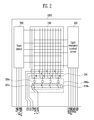
- FIG. 2 is a schematic structural view of an organic light emitting display in a lighting test according to aspects of the present invention
- FIG. 3A is a structural view showing a signal transfer unit according to aspects of the present invention.
- FIG. 3B is a circuit diagram of aspects of the signal transfer unit of FIG. 3A ;
- FIG. 3C is a further circuit diagram of aspects of the signal transfer unit of FIG. 3A ;
- FIG. 4A is a further structural view showing a signal transfer unit according to aspects of the present invention.
- FIG. 4B is a circuit diagram of aspects of the signal transfer unit of FIG. 4A ;
- FIG. 5A is a structural view showing a signal transfer unit according to aspects of the present invention.
- FIG. 5B is a circuit diagram of aspects of the signal transfer unit of FIG. 5A ;
- FIG. 6 is a cross-sectional diagram of aspects of an organic light emitting display according to aspects of the present invention.
- FIG. 1 is a schematic structural view of an organic light emitting display according to aspects of the present invention.
- an organic light emitting display includes a display unit (or display region) 100, a data driver 200, a scan driver 300, and a light emission control driver 400.
- the display unit 100 includes a plurality of pixels 101. Each pixel 101 includes an organic light emitting diode. The organic light emitting diode emits light corresponding to current flow in the diode.
- the display unit 100 has n scan lines S1, S2, ..., Sn-1, and Sn extending in a row direction for transferring scan signals.
- the display unit 100 has m data lines D1, D2, ..., Dm-1, and Dm extending in a column direction for transferring data signals.
- the data driver 200 generates data signals from image signals having red, blue, and green (R, G, B) components.
- the data driver 200 applies the generated data signals to the data lines D1, D2, ..., Dm-1, and Dm of the display unit 100.
- the data signals output from the data driver 200 may use multiplexing in order to reduce the number of output terminals of the data driver 200.
- the scan driver 300 generates the scan signals and is coupled to the scan signals S1, S2, ..., Sn-1, and Sn to transfer the scan signals to a specific row of the display unit 100.
- the scan signals are synchronized with the data signals output from the data driver 200 so that voltage corresponding to the data signals is transferred to the proper pixel 101.
- the light emission control driver 400 generates light emission control signals and is coupled to light emission control lines E1, E2, ... En-1, and En to transfer the light emission control signals to a specific row of the display unit 100.
- the pixel 101 is coupled to a corresponding light emission control signal so that driving current is generated corresponding to the voltage generated by the data signals. The generated driving current flows to the organic light emitting diode in the pixel 101.
- the display unit 100 receives a first power and a second power.
- the display unit 100 allows current to flow in the organic light emitting diode using the scan signals, the data signals, the light emission control signals, and the first power and second power to emit light, thereby displaying an image.
- a lighting test is performed on the organic light emitting display in order to judge whether each pixel operates properly.
- the lighting test simply examines whether the pixel operates, thus data writing using the data driver 200 is not necessary. Therefore, the lighting test may be performed according to the structure shown in FIG. 2 .
- the lighting test may be performed before a data driver IC is mounted on the organic light emitting display.
- FIG. 2 is a schematic structural view of an organic light emitting display in a lighting test.
- a display unit 100, a scan driver 300, and a light emission control driver 400 are on a transparent substrate 1000.
- the transparent substrate 1000 includes an IC region 200a.
- IC region 200a includes a plurality of terminals 220a to be coupled with pins of a data driver.
- a multiplex unit 250 is between the display unit 100 and the IC region 200a so that three data lines are coupled to one of the plurality of terminals 220a in the IC region 200a through the multiplex unit 250.
- Other embodiments may not have a multiplex unit and thus have data lines coupled to the plurality of terminals without an intervening multiplex unit.
- a plurality of wires for transferring signals for controlling the scan driver 300, the light emission control driver 400, and the multiplex unit 250 are included on the transparent substrate 1000 so that the signals are transferred to the scan driver 300, the light emission control driver 400, and the multiplex unit 250 from sources external to the substrate 1000.
- the display unit 100 is depicted as having a very few signal lines for illustrative purposes, in practice, the display unit 100 would include many hundreds of the lines in both row and column directions, as those skilled in the art would appreciate. Of course, an appropriate number of driving circuits would be provided to drive such signal lines.
- the IC region 200a is a substantially vacant space since a data driver is not yet on the organic light emitting display.
- a signal transfer unit for transferring lighting signals is provided in the IC region 200a.
- the signal transfer unit includes a plurality of transistors 210a for receiving lighting test signals from sources external to the display and transferring the lighting test signals to each pixel.
- the signal transfer unit also includes a protection unit 210b for reducing or preventing damage from static electricity. Although a single protection unit is shown in FIG. 2 , some embodiments may use multiple protection units.
- the signal transfer unit is coupled to lighting test signals external to the display through wires.
- the scan driver 300, the light emission control driver 400, the multiplex unit 250, and the signal transfer unit are driven to perform a lighting text on the organic light emitting display.
- the signal transfer unit on the transparent substrate 1000 is formed at the same time the display unit 100 is formed. That is, the display unit 100 and the signal transfer unit are formed on the transparent substrate 1000 through the same process.
- the scan driver 300 and the light emission control driver 400 may also be formed by the same process that forms the display unit 100 and the signal transfer unit.
- the organic light emitting display may be subjected to static electricity during the manufacturing process, and the transistors 210a of the signal transfer unit and transistors of the display unit 100 may be damaged by the static electricity. If the display unit 100 is damaged, defects are generated in the product, and if the signal transfer unit is damaged, the lighting test cannot be performed. In order to avoid such problems, the protection unit 210b is formed in the signal transfer unit. The protection unit 210b protects the pixel and/or the signal transfer unit from static electricity transferred during the manufacturing process of the organic light emitting display.
- FIGs. 3A, 3B, and 3C show aspects of an embodiment of the signal transfer unit.
- FIG. 3A shows structural aspects of the signal transfer unit.
- FIG. 3B shows a circuit diagram of the signal transfer unit.
- FIG. 3C show an equivalent circuit diagram of the signal transfer unit.
- a signal transfer unit includes a plurality of transistors 210a for transferring lighting signals and a protection unit 210b for protecting the plurality of transistors 210a and other elements from static electricity.
- the plurality of transistors 210a are coupled to a plurality of terminals 220a (to which a data driver is to be coupled after the lighting test) that are also coupled to data lines of a display unit 100.
- the protection unit 210b of the invention electrically connects the source and drain to the gate of transistor 210a.
- a circuit as shown in FIG. 3B is formed. With the source and drain connected to the gate of transistor 210a via a metal, i.e. the gate metal, the transistor is diode-connected so that it may be represented as shown in FIG. 3C .
- a transistor serves as a diode if the source and drain are equivalent in potential to the gate, which they are in the first embodiment since the source and the drain are connected to the gate via the gate metal. Thus, the transistor functions as a diode.
- the source and drain are connected to the gate of transistor 210a via a resistor formed by a semiconductor. A voltage drop occurs owing to the resistor so that the source and drain do not have equivalent potential to the gate. Thus, in the second embodiment, the transistor performs its own transistor operation.
- a fabrication process of the pixels 101 of display unit 100 of FIGS. 1 and 2 will now be described with reference to FIG. 6 .
- a semiconductor layer 601 for example, polysilicon, is formed and patterned over a buffer layer 623 on a substrate 1000 to create channel regions.
- a first insulating film 603 is formed thereon.
- a first metal layer 605 is then formed and patterned to create gate metals.
- a second insulating film 607 is formed on the gate metals.
- a second metal layer 609 is formed and patterned to create source-drain metals.
- Contact holes 611 are formed in the insulating films to couple the source-drain metals to the channel regions or to the gate metals.
- a planarization layer 625 is formed over source-drain metals and the second insulating film 607.
- a pixel definition film 613 is formed over the planarization layer 625.
- a transparent metal film 615 for example, ITO, is formed and patterned on the pixel definition film 613 to create anode electrodes.
- An organic light emitting layer 617 is formed on the anode electrodes and a cathode electrode 619 is formed over the organic light emitting layer 617.
- the signal transfer unit is formed through the same process used in the forming of the display unit 100. Referring to FIG. 3A , when the channel regions of thin film transistors of the display unit 100 are formed, channel regions cr of the transistors 210a included in the signal transfer unit are also formed.
- the first insulating film is formed on the channel regions cr.
- Gate metals gm are created on the first insulating film.
- the gate metals gm are gate electrodes of the transistors 210a.
- the protection unit 210b also includes gate metal gm.
- Gate metal of the protection unit 210b has a snake-like or meander-like shape to allow length to be increased within a small area. Increased length increases resistance of the protection unit 210b.
- a contact hole h1 is formed in the second insulating film to couple the source-drain metals sdm to the gate metal gm forming the protection unit 210b.
- the structure and the circuit of the signal transfer unit as shown in FIGs. 3A and 3B are formed.
- the protection unit 210b of the signal transfer unit is removed through the etching process. Galvanic effect may be used for etching the anode electrodes and removing the protection unit 210b. After the removal of the protection unit 210b, the structure of the signal transfer unit becomes a structure as shown in FIG. 4A . However, the protection unit 210b may not be etched completely but a portion of it may remain after etching. This remaining portion is preferably the end of the protection unit 210b opposite to the transistors 210a where the gate metal changes its direction to connect the source and drain to the gate of the transistors.
- the signal transfer unit includes the transistors 210a as shown in FIG. 4B . Therefore, signals can be transferred to the display unit 100 from a source external to the organic light emitting display through the transistors 210a, making it possible to perform the lighting test.
- the protection unit 210b of the signal transfer unit protects the display unit 100 and the plurality of transistors 210a of the signal transfer unit from being damaged by static electricity.
- the process by which the protection unit 210b reduces or prevents damage due to static electricity is as follows. If static electricity is transferred to the plurality of transistors 210a of the signal transfer unit, due to the diode connection of the transistors, static electricity is not transferred to the pixels 101. Since the protection unit 210b is made of a conductive material, such as source-drain metal sdm or gate metal gm, static electricity is transferred to the source-drain metal sdm and the gate metal gm.
- the second insulating film positioned between the source-drain metal sdm and the gate metal gm is burned off such that the metals are shorted together thereby dissipating the static electricity. Therefore, only the protection unit 210b is damaged by static electricity. Accordingly, the transistors 210a of the signal transfer unit and the transistor of the display unit 100 are protected.
- FIG. 5A is a structural view showing another embodiment of the signal transfer unit of FIG. 2
- FIG. 5B is a circuit diagram of the signal transfer unit of FIG. 5A
- the signal transfer unit includes a plurality of transistors 210a for transferring lighting test signals from an external source and a protection unit 210b for protecting the plurality of transistors 201 a and pixels 101.
- the protection unit 210b includes or consists of a resistor with the resistor coupled to the plurality of transistors 210a as before.
- high voltage of the static electricity is dissipated by the resistor.
- at least one transistor of the plurality of transistors 210a of the signal transfer unit is a dummy transistor that functions to protect other transistors from being damaged by static electricity. Dummy transistors are not configured to transfer the lighting test signals.
- the fabrication process of the plurality of transistors 210a and protection unit 210b of the signal transfer unit is now described.
- channel regions of the thin film transistors of the display unit 100 are formed, channel regions cr of the plurality of transistors 210a and of the protection unit 210b of the signal transfer unit are also formed.
- the channel regions cr are formed of a semiconductor layer.
- a first insulating film is formed on the channel regions cr. Gate metals gm are formed thereon. The gate metals gm become gate electrodes of the plurality of transistors 210a. A contact hole h2 is formed in the first insulating film to couple the protection unit to the gate metal gm. Likewise, the gate metal gm is formed for the protection unit 210b. After the gate metals gm are formed, an ion doping process is performed. Channel regions cr below gate metals gm are blocked from ion doping so that they remain intrinsic semiconductor regions. Therefore, the protection unit 210b has a high resistance value.
- the channel region of the protection unit 210b has a snake-like or meander-like shape to allow length to be increased in a small area.
- source-drain metals sdm of the plurality of transistors 210a of the display unit 100 are formed, source-drain metals sdm of the transistors of the signal transfer unit are also formed.
- a contact hole h3 is formed in the second insulating film to couple the source-drain metals sdm to the channel regions cr forming the protection unit 210b. Therefore, as shown in FIG. 5B , the resistor is coupled in parallel with the plurality of transistors 210a of the signal transfer unit.
- the making of the display may comprise patterning semiconductor layers on a substrate 1000 to form first channel region of a plurality of transistors 210a of a signal transfer unit 200 for transferring lighting test signals to a display region 100 of the display and a second channel region of a protection unit 210b to protect the transistors from static electricity. Then, a first insulating film 603 on the substrate 1000 and on the first and second channel regions may be formed. A first metal layer 605 may be patterned on the first insulating film 603 to form a first gate metal formed on the first channel region and a second gate metal formed on the second channel region, one end of the first gate metal being coupled to that of the second channel region.
- a second insulating film 607 may be formed on the first insulating film 603 and on the first and second gate metals. And a second metal layer 609 may be patterned on the second insulating film 607 to form source-drain metals sdm, one end of the source-drain metals sdm being coupled to that of the second channel region
- the protection unit 210b is not removed while completing the display unit.
- the signal transfer unit is formed with the plurality of transistors 210a and a resistor so that there is no need to remove the protection unit 210b.
- the diode-connection of the first-embodiment needs to be removed before the lighting-test is performed.
Landscapes
- Engineering & Computer Science (AREA)
- Physics & Mathematics (AREA)
- Computer Hardware Design (AREA)
- General Physics & Mathematics (AREA)
- Theoretical Computer Science (AREA)
- Microelectronics & Electronic Packaging (AREA)
- Geometry (AREA)
- Manufacturing & Machinery (AREA)
- Electroluminescent Light Sources (AREA)
- Devices For Indicating Variable Information By Combining Individual Elements (AREA)
- Thin Film Transistor (AREA)
- Control Of Indicators Other Than Cathode Ray Tubes (AREA)
Abstract

Description
- The present invention relates to an organic light emitting display and a method for making the same.
- Recently, various flat panel display devices that are reduced in weight and volume, in comparison to a cathode ray tube (CRT), have been developed. Types of flat panel display devices include liquid crystal display, field emission display, plasma display panel, and organic light emitting display.
- The organic light emitting display displays an image using organic light emitting diodes (OLEDs) and generates light by recombination of electrons and holes generated corresponding to a flow of current. The organic light emitting display has excellent color reproducibility and a thin thickness. Organic light emitting displays often control flow of current to organic light emitting diodes using thin film transistors.
- During manufacturing of an organic light emitting display, static electricity may be generated. If the static electricity is transferred to a thin film transistor in the display, the thin film transistor may be damaged and its properties are degraded, thereby causing failure or deterioration of image quality of the organic light emitting display. During organic light emitting display manufacturing it is often desirable to perform a lighting test to test operation of display pixels; however, damage from static electricity may interfere with the lighting test.
- Aspects of embodiments of the present invention are directed toward an organic light emitting display and a method for making the same that forms a structure for preventing or reducing damage from static electricity during a manufacturing process, thereby protecting the display and facilitating a lighting test.
- An embodiment of the present invention provides an organic light emitting display including: a substrate; a display region on the substrate, the display region including a plurality of pixels; and a signal transfer unit on the substrate for transferring lighting test signals to the plurality of pixels, wherein the signal transfer unit includes a plurality of transistors for transferring the lighting test signals, and a resistor coupled to drains and gates of the plurality of transistors for protecting the plurality of transistors.
- Another embodiment of the present invention provides a method for making an organic light emitting display, the method including: patterning a semiconductor layer on a substrate to form channel regions; forming a first insulating film on the substrate and on the channel regions; patterning a first metal layer on the first insulating film to form gate metals; forming a second insulating film on the first insulating film and on the gate metals; and patterning a second metal layer on the second insulating film to form source-drain metals, wherein an end of the source-drain metals is coupled to an end of the gate metals.
- Another embodiment of the present invention provides a method for making an organic light emitting display, the method including: patterning semiconductor layers on a substrate to form a first channel region and a second channel region; forming a first insulating film on the substrate and on the first and second channel regions; patterning a first metal layer on the first insulating film to form a first gate metal formed on the first channel region and a second gate metal formed on the second channel region, one end of the first gate metal being coupled to that of the second gate metal; forming a second insulating film on the first insulating film and on the first and second gate metals; and patterning a second metal layer on the second insulating film to form source-drain metals, one end of the source-drain metals being coupled to that of the second channel region.
- The accompanying drawings, together with the specification, illustrate exemplary embodiments of the present invention, and, together with the description, serve to explain the principles of the present invention.
-
FIG. 1 is a schematic structural view of an organic light emitting display according to aspects of the present invention; -
FIG. 2 is a schematic structural view of an organic light emitting display in a lighting test according to aspects of the present invention; -
FIG. 3A is a structural view showing a signal transfer unit according to aspects of the present invention; -
FIG. 3B is a circuit diagram of aspects of the signal transfer unit ofFIG. 3A ; -
FIG. 3C is a further circuit diagram of aspects of the signal transfer unit ofFIG. 3A ; -
FIG. 4A is a further structural view showing a signal transfer unit according to aspects of the present invention; -
FIG. 4B is a circuit diagram of aspects of the signal transfer unit ofFIG. 4A ; -
FIG. 5A is a structural view showing a signal transfer unit according to aspects of the present invention; -
FIG. 5B is a circuit diagram of aspects of the signal transfer unit ofFIG. 5A ; and -
FIG. 6 is a cross-sectional diagram of aspects of an organic light emitting display according to aspects of the present invention. - In the following detailed description, only certain exemplary embodiments of the present invention have been shown and described, simply by way of illustration. As those skilled in the art would realize, the described embodiments may be modified in various different ways, all without departing from the scope of the present invention. Accordingly, the drawings and description are to be regarded as illustrative in nature and not restrictive. Like reference numerals designate like elements throughout the specification.
- Throughout this specification and the claims that follow, when an element is referred to as being "on" another element, it may be directly on the another element or it may be indirectly on the another element with one or more intervening elements interposed therebetween. Also, when an element is referred to as being "coupled" to another element, it may be directly coupled to the another element or may be indirectly coupled to the another element with one or more intervening elements interposed therebetween.
-
FIG. 1 is a schematic structural view of an organic light emitting display according to aspects of the present invention. Referring toFIG. 1 , an organic light emitting display includes a display unit (or display region) 100, adata driver 200, ascan driver 300, and a lightemission control driver 400. - The
display unit 100 includes a plurality ofpixels 101. Eachpixel 101 includes an organic light emitting diode. The organic light emitting diode emits light corresponding to current flow in the diode. Thedisplay unit 100 has n scan lines S1, S2, ..., Sn-1, and Sn extending in a row direction for transferring scan signals. Thedisplay unit 100 has m data lines D1, D2, ..., Dm-1, and Dm extending in a column direction for transferring data signals. - The
data driver 200 generates data signals from image signals having red, blue, and green (R, G, B) components. Thedata driver 200 applies the generated data signals to the data lines D1, D2, ..., Dm-1, and Dm of thedisplay unit 100. The data signals output from thedata driver 200 may use multiplexing in order to reduce the number of output terminals of thedata driver 200. - The
scan driver 300 generates the scan signals and is coupled to the scan signals S1, S2, ..., Sn-1, and Sn to transfer the scan signals to a specific row of thedisplay unit 100. The scan signals are synchronized with the data signals output from thedata driver 200 so that voltage corresponding to the data signals is transferred to theproper pixel 101. - The light
emission control driver 400 generates light emission control signals and is coupled to light emission control lines E1, E2, ... En-1, and En to transfer the light emission control signals to a specific row of thedisplay unit 100. Thepixel 101 is coupled to a corresponding light emission control signal so that driving current is generated corresponding to the voltage generated by the data signals. The generated driving current flows to the organic light emitting diode in thepixel 101. - Also, the
display unit 100 receives a first power and a second power. Thedisplay unit 100 allows current to flow in the organic light emitting diode using the scan signals, the data signals, the light emission control signals, and the first power and second power to emit light, thereby displaying an image. - A lighting test is performed on the organic light emitting display in order to judge whether each pixel operates properly. The lighting test simply examines whether the pixel operates, thus data writing using the
data driver 200 is not necessary. Therefore, the lighting test may be performed according to the structure shown inFIG. 2 . By way of example, the lighting test may be performed before a data driver IC is mounted on the organic light emitting display. -
FIG. 2 is a schematic structural view of an organic light emitting display in a lighting test. Referring toFIG. 2 , adisplay unit 100, ascan driver 300, and a lightemission control driver 400 are on atransparent substrate 1000. Thetransparent substrate 1000 includes anIC region 200a.IC region 200a includes a plurality ofterminals 220a to be coupled with pins of a data driver. Also, amultiplex unit 250 is between thedisplay unit 100 and theIC region 200a so that three data lines are coupled to one of the plurality ofterminals 220a in theIC region 200a through themultiplex unit 250. Other embodiments may not have a multiplex unit and thus have data lines coupled to the plurality of terminals without an intervening multiplex unit. Also, a plurality of wires for transferring signals for controlling thescan driver 300, the lightemission control driver 400, and themultiplex unit 250 are included on thetransparent substrate 1000 so that the signals are transferred to thescan driver 300, the lightemission control driver 400, and themultiplex unit 250 from sources external to thesubstrate 1000. While thedisplay unit 100 is depicted as having a very few signal lines for illustrative purposes, in practice, thedisplay unit 100 would include many hundreds of the lines in both row and column directions, as those skilled in the art would appreciate. Of course, an appropriate number of driving circuits would be provided to drive such signal lines. - During the lighting test in one embodiment, the
IC region 200a is a substantially vacant space since a data driver is not yet on the organic light emitting display. During the lighting test, a signal transfer unit for transferring lighting signals is provided in theIC region 200a. The signal transfer unit includes a plurality oftransistors 210a for receiving lighting test signals from sources external to the display and transferring the lighting test signals to each pixel. The signal transfer unit also includes aprotection unit 210b for reducing or preventing damage from static electricity. Although a single protection unit is shown inFIG. 2 , some embodiments may use multiple protection units. The signal transfer unit is coupled to lighting test signals external to the display through wires. - After the organic light emitting display is implemented as described above, the
scan driver 300, the lightemission control driver 400, themultiplex unit 250, and the signal transfer unit are driven to perform a lighting text on the organic light emitting display. - The signal transfer unit on the
transparent substrate 1000 is formed at the same time thedisplay unit 100 is formed. That is, thedisplay unit 100 and the signal transfer unit are formed on thetransparent substrate 1000 through the same process. Thescan driver 300 and the lightemission control driver 400 may also be formed by the same process that forms thedisplay unit 100 and the signal transfer unit. - The organic light emitting display may be subjected to static electricity during the manufacturing process, and the
transistors 210a of the signal transfer unit and transistors of thedisplay unit 100 may be damaged by the static electricity. If thedisplay unit 100 is damaged, defects are generated in the product, and if the signal transfer unit is damaged, the lighting test cannot be performed. In order to avoid such problems, theprotection unit 210b is formed in the signal transfer unit. Theprotection unit 210b protects the pixel and/or the signal transfer unit from static electricity transferred during the manufacturing process of the organic light emitting display. -
FIGs. 3A, 3B, and 3C show aspects of an embodiment of the signal transfer unit.FIG. 3A shows structural aspects of the signal transfer unit.FIG. 3B shows a circuit diagram of the signal transfer unit.FIG. 3C show an equivalent circuit diagram of the signal transfer unit. ExplainingFIG. 3A with reference toFIGS. 3B and 3C , a signal transfer unit includes a plurality oftransistors 210a for transferring lighting signals and aprotection unit 210b for protecting the plurality oftransistors 210a and other elements from static electricity. The plurality oftransistors 210a are coupled to a plurality ofterminals 220a (to which a data driver is to be coupled after the lighting test) that are also coupled to data lines of adisplay unit 100. - The
protection unit 210b of the invention electrically connects the source and drain to the gate oftransistor 210a. In a first embodiment, a circuit as shown inFIG. 3B is formed. With the source and drain connected to the gate oftransistor 210a via a metal, i.e. the gate metal, the transistor is diode-connected so that it may be represented as shown inFIG. 3C . A transistor serves as a diode if the source and drain are equivalent in potential to the gate, which they are in the first embodiment since the source and the drain are connected to the gate via the gate metal. Thus, the transistor functions as a diode. In the second embodiment ofFig. 5 , the source and drain are connected to the gate oftransistor 210a via a resistor formed by a semiconductor. A voltage drop occurs owing to the resistor so that the source and drain do not have equivalent potential to the gate. Thus, in the second embodiment, the transistor performs its own transistor operation. - A fabrication process of the
pixels 101 ofdisplay unit 100 ofFIGS. 1 and2 will now be described with reference toFIG. 6 . Asemiconductor layer 601, for example, polysilicon, is formed and patterned over abuffer layer 623 on asubstrate 1000 to create channel regions. A first insulatingfilm 603 is formed thereon. Afirst metal layer 605 is then formed and patterned to create gate metals. A secondinsulating film 607 is formed on the gate metals. Asecond metal layer 609 is formed and patterned to create source-drain metals. Contact holes 611 are formed in the insulating films to couple the source-drain metals to the channel regions or to the gate metals. Aplanarization layer 625 is formed over source-drain metals and the secondinsulating film 607. A pixel definition film 613 is formed over theplanarization layer 625. Atransparent metal film 615, for example, ITO, is formed and patterned on the pixel definition film 613 to create anode electrodes. An organiclight emitting layer 617 is formed on the anode electrodes and a cathode electrode 619 is formed over the organiclight emitting layer 617. - In the first embodiment, the signal transfer unit is formed through the same process used in the forming of the
display unit 100. Referring toFIG. 3A , when the channel regions of thin film transistors of thedisplay unit 100 are formed, channel regions cr of thetransistors 210a included in the signal transfer unit are also formed. - The first insulating film is formed on the channel regions cr. Gate metals gm are created on the first insulating film. The gate metals gm are gate electrodes of the
transistors 210a. Theprotection unit 210b also includes gate metal gm. Gate metal of theprotection unit 210b has a snake-like or meander-like shape to allow length to be increased within a small area. Increased length increases resistance of theprotection unit 210b. When the source-drain metals of the transistors of thedisplay unit 100 are formed, source-drain metals sdm of the plurality oftransistors 210a of the signal transfer unit are also formed. A contact hole h1 is formed in the second insulating film to couple the source-drain metals sdm to the gate metal gm forming theprotection unit 210b. Thus, the structure and the circuit of the signal transfer unit as shown inFIGs. 3A and 3B are formed. - When the anode electrodes of the
display unit 100 are patterned through etching, theprotection unit 210b of the signal transfer unit is removed through the etching process. Galvanic effect may be used for etching the anode electrodes and removing theprotection unit 210b. After the removal of theprotection unit 210b, the structure of the signal transfer unit becomes a structure as shown inFIG. 4A . However, theprotection unit 210b may not be etched completely but a portion of it may remain after etching. This remaining portion is preferably the end of theprotection unit 210b opposite to thetransistors 210a where the gate metal changes its direction to connect the source and drain to the gate of the transistors. - After the
protection unit 210b is removed, the lighting test is performed. The signal transfer unit includes thetransistors 210a as shown inFIG. 4B . Therefore, signals can be transferred to thedisplay unit 100 from a source external to the organic light emitting display through thetransistors 210a, making it possible to perform the lighting test. - The
protection unit 210b of the signal transfer unit protects thedisplay unit 100 and the plurality oftransistors 210a of the signal transfer unit from being damaged by static electricity. The process by which theprotection unit 210b reduces or prevents damage due to static electricity is as follows. If static electricity is transferred to the plurality oftransistors 210a of the signal transfer unit, due to the diode connection of the transistors, static electricity is not transferred to thepixels 101. Since theprotection unit 210b is made of a conductive material, such as source-drain metal sdm or gate metal gm, static electricity is transferred to the source-drain metal sdm and the gate metal gm. When static electricity is high voltage, the second insulating film positioned between the source-drain metal sdm and the gate metal gm is burned off such that the metals are shorted together thereby dissipating the static electricity. Therefore, only theprotection unit 210b is damaged by static electricity. Accordingly, thetransistors 210a of the signal transfer unit and the transistor of thedisplay unit 100 are protected. -
FIG. 5A is a structural view showing another embodiment of the signal transfer unit ofFIG. 2 , andFIG. 5B is a circuit diagram of the signal transfer unit ofFIG. 5A . As in the first embodiment, referring toFIGS. 5A and 5B , the signal transfer unit includes a plurality oftransistors 210a for transferring lighting test signals from an external source and aprotection unit 210b for protecting the plurality of transistors 201 a andpixels 101. Theprotection unit 210b includes or consists of a resistor with the resistor coupled to the plurality oftransistors 210a as before. When static electricity is transferred to the signal transfer unit, high voltage of the static electricity is dissipated by the resistor. Again, at least one transistor of the plurality oftransistors 210a of the signal transfer unit is a dummy transistor that functions to protect other transistors from being damaged by static electricity. Dummy transistors are not configured to transfer the lighting test signals. - The fabrication process of the plurality of
transistors 210a andprotection unit 210b of the signal transfer unit is now described. When channel regions of the thin film transistors of thedisplay unit 100 are formed, channel regions cr of the plurality oftransistors 210a and of theprotection unit 210b of the signal transfer unit are also formed. The channel regions cr are formed of a semiconductor layer. - A first insulating film is formed on the channel regions cr. Gate metals gm are formed thereon. The gate metals gm become gate electrodes of the plurality of
transistors 210a. A contact hole h2 is formed in the first insulating film to couple the protection unit to the gate metal gm. Likewise, the gate metal gm is formed for theprotection unit 210b. After the gate metals gm are formed, an ion doping process is performed. Channel regions cr below gate metals gm are blocked from ion doping so that they remain intrinsic semiconductor regions. Therefore, theprotection unit 210b has a high resistance value. For higher resistance value, the channel region of theprotection unit 210b has a snake-like or meander-like shape to allow length to be increased in a small area. When the source-drain metals sdm of the plurality oftransistors 210a of thedisplay unit 100 are formed, source-drain metals sdm of the transistors of the signal transfer unit are also formed. A contact hole h3 is formed in the second insulating film to couple the source-drain metals sdm to the channel regions cr forming theprotection unit 210b. Therefore, as shown inFIG. 5B , the resistor is coupled in parallel with the plurality oftransistors 210a of the signal transfer unit. - The making of the display may comprise patterning semiconductor layers on a
substrate 1000 to form first channel region of a plurality oftransistors 210a of asignal transfer unit 200 for transferring lighting test signals to adisplay region 100 of the display and a second channel region of aprotection unit 210b to protect the transistors from static electricity. Then, a firstinsulating film 603 on thesubstrate 1000 and on the first and second channel regions may be formed. Afirst metal layer 605 may be patterned on the first insulatingfilm 603 to form a first gate metal formed on the first channel region and a second gate metal formed on the second channel region, one end of the first gate metal being coupled to that of the second channel region. A secondinsulating film 607 may be formed on the first insulatingfilm 603 and on the first and second gate metals. And asecond metal layer 609 may be patterned on the secondinsulating film 607 to form source-drain metals sdm, one end of the source-drain metals sdm being coupled to that of the second channel region - In this embodiment, the
protection unit 210b is not removed while completing the display unit. The signal transfer unit is formed with the plurality oftransistors 210a and a resistor so that there is no need to remove theprotection unit 210b. In contrast, the diode-connection of the first-embodiment needs to be removed before the lighting-test is performed. - The process of reducing or preventing damage due to static electricity by the
protection unit 210b of the signal transfer unit will now be explained for the second embodiment. If static electricity is transferred to the signal transfer unit, the static electricity is transferred to the resistor coupled to the plurality oftransistors 210a of the signal transfer unit. Therefore, the static electricity is dissipated by the resistor, making it possible to reduce or prevent damage due to the static electricity. - While the present invention has been described in connection with certain exemplary embodiments, it is to be understood that the invention is not limited to the disclosed embodiments, but, on the contrary, is intended to cover various modifications and equivalent arrangements included within the scope of the appended claims, and equivalents thereof.
Claims (18)
- An organic light emitting display comprising:a substrate (1000);a display region (100) on the substrate (1000), the display region (100) comprising a plurality of pixels (101); anda signal transfer unit on the substrate (1000) for transferring lighting test signals to the plurality of pixels (101),wherein the signal transfer unit comprises a plurality of transistors (210a) for transferring the lighting test signals, and a resistor (210b) electrically coupling the drains and gates of the plurality of transistors (210a) for protecting the plurality of transistors (210a) from static electricity.
- The organic light emitting display as claimed in claim 1, wherein the resistor (210b) comprises an intrinsic semiconductor coupled in parallel to the plurality of transistors (220a).
- The organic light emitting display as claimed in claim 1 or 2, wherein the plurality of transistors (210a) of the signal transfer unit comprises:channel regions (cr) on the substrate (1000), the channel regions (cr) comprising a semiconductor layer (601);a first insulating film (603) on the channel regions (cr) and the substrate (1000);gate metals (gm) on the first insulating film (603), the gate metals (gm) comprising a first metal layer (605), wherein the gate metals (gm) are coupled to an end of the resistor(210b);a second insulating film (607) on the gate metals (gm) and the first insulating film (603); andsource-drain metals (sdm) on the second insulating film (607), the source-drain metals (sdm) comprising a second metal layer (609), wherein the source-drain metals (sdm) are coupled to the channel regions (cr) and coupled to another end of the resistor (210b).
- The organic light emitting display as claimed in claim 3, wherein the resistor (210b) comprises the same semiconductor layer (601) as the channel regions (cr) of the plurality of transistors (210a).
- The organic light emitting display as claimed in one of the previous claims, wherein at least one transistor (210a) of the plurality of transistors is not configured for transferring the lighting test signals.
- The organic light emitting display as claimed in one of the previous claims, wherein a data driver (200) is coupled to a region on the substrate (1000) where the signal transfer unit is positioned.
- The organic light emitting display as claimed in one of the previous claims, wherein gate metals (gm) are formed on the resistor (210b).
- A method for making an organic light emitting display, the method comprising:patterning a semiconductor layer (601) on a substrate (1000) to form channel regions (cr) of a plurality of transistors (210a) of a signal transfer unit (200) for transferring lighting test signals to a display region (100) of the display;forming a first insulating film (603) on the substrate (1000) and on the channel regions (cr);patterning a first metal layer (605) on the first insulating film (603) to form gate metals (gm);forming a second insulating film (607) on the first insulating film (603) and on the gate metals (gm); andpatterning a second metal layer (609) on the second insulating film (607) to form source-drain metals (sdm);
characterized byforming a protection unit (210b) by electrically coupling an end of the source-drain metals (sdm) of the transistors (210a) of the signal transfer unit to an end of the gate metals (gm) of said transistors (210a). - The method as claimed in claim 8, further comprising etching of the protection unit (210b) in an area where the source-drain metals (sdm) are coupled to the gate metals (gm).
- The method as claimed in claim 9, wherein after the etching is performed, a data driver (200) is connected to the display device.
- The method as claimed in one of the previous claims 8-10, wherein the coupling between the end of the source-drain metals (sdm) and an extended end of the gate metals (gm) is through a contact hole (h1) in the second insulating film (607).
- The method of one of the previous claims 8-11, wherein the protection unit (210b) includes gate metal (gm) itself provided in a meander-like shape and electrically coupling the gate metal (gm) of the transistors (210a) and the source-drain metal (sdm) of the transistors (210a) providing a diode-connection between the gates and source-drains of the transistors (210a).
- A method for making an organic light emitting display, the method comprising:patterning semiconductor layers on a substrate (1000) to form a first channel region of a plurality of transistors (210a) of a signal transfer unit (200) for transferring lighting test signals to a display region (100) of the display and a second channel region of a protection unit (210b) to protect the transistors from static electricity;forming a first insulating film (603) on the substrate (1000) and on the first and second channel regions;patterning a first metal layer (605) on the first insulating film (603) to form a first gate metal formed on the first channel region and a second gate metal formed on the second channel region, one end of the first gate metal being coupled to that of the second channel region;forming a second insulating film (607) on the first insulating film (603) and on the first and second gate metals; andpatterning a second metal layer (609) on the second insulating film (607) to form source-drain metals (sdm), one end of the source-drain metals (sdm) being coupled to that of the second channel region.
- The method as claimed in claim 13, wherein the second gate metal covers substantially an entire area of the second channel region.
- The method as claimed in claim 13 or claim 8, further comprising performing an ion doping process after the patterning the first metal layer.
- The method as claimed in claim 13, wherein the second channel region comprises or consists of an intrinsic semiconductor.
- The method of claims 13-16, wherein the connection between the source-drains and gates of the transistors (210a) via the second channel region is provided through a second contact hole (h2) formed in the first insulating film to couple the second channel region to the gate metal (gm) and a third contact hole (h3) formed in the second insulating film to couple the source-drain metal (sdm) to the second channel regions.
- An intermediate product of the making of an organic light emitting display, wherein the intermediate product is formed by the method of one of the claims 8 to 12 or by the method of one of the claims 13-17.
Applications Claiming Priority (1)
| Application Number | Priority Date | Filing Date | Title |
|---|---|---|---|
| KR1020080044454A KR100941835B1 (en) | 2008-05-14 | 2008-05-14 | Organic light emitting display device and manufacturing method |
Publications (2)
| Publication Number | Publication Date |
|---|---|
| EP2120265A1 true EP2120265A1 (en) | 2009-11-18 |
| EP2120265B1 EP2120265B1 (en) | 2014-03-19 |
Family
ID=40902113
Family Applications (1)
| Application Number | Title | Priority Date | Filing Date |
|---|---|---|---|
| EP09160218.5A Active EP2120265B1 (en) | 2008-05-14 | 2009-05-14 | Organic light emitting display and method for making the same |
Country Status (5)
| Country | Link |
|---|---|
| US (1) | US7888683B2 (en) |
| EP (1) | EP2120265B1 (en) |
| JP (1) | JP4920644B2 (en) |
| KR (1) | KR100941835B1 (en) |
| CN (1) | CN101582439B (en) |
Cited By (1)
| Publication number | Priority date | Publication date | Assignee | Title |
|---|---|---|---|---|
| EP2299431A1 (en) * | 2009-09-02 | 2011-03-23 | Samsung Mobile Display Co., Ltd. | Organic light emitting display device |
Families Citing this family (12)
| Publication number | Priority date | Publication date | Assignee | Title |
|---|---|---|---|---|
| KR101181007B1 (en) | 2009-12-02 | 2012-09-07 | 현대자동차주식회사 | Muffler for vehicle |
| JP6037261B2 (en) * | 2012-01-23 | 2016-12-07 | 株式会社ジャパンディスプレイ | Display device |
| KR101884891B1 (en) * | 2012-02-08 | 2018-08-31 | 삼성디스플레이 주식회사 | Display device |
| KR101985921B1 (en) * | 2012-06-13 | 2019-06-05 | 삼성디스플레이 주식회사 | Organic light emitting diode display |
| KR101975569B1 (en) * | 2012-10-15 | 2019-05-08 | 삼성디스플레이 주식회사 | Circuit for preventing static electricity of a display panel and display device comprising the same |
| KR102270632B1 (en) | 2015-03-04 | 2021-06-30 | 삼성디스플레이 주식회사 | Display panel, display device and mtehod for driving display panel |
| CN104835837B (en) * | 2015-06-05 | 2017-07-28 | 杭州士兰微电子股份有限公司 | High-voltage semi-conductor device and its manufacture method |
| CN105206601B (en) | 2015-10-19 | 2019-03-12 | 京东方科技集团股份有限公司 | Test component unit, array substrate, display panel, display device, and method of manufacturing test component unit |
| CN106292097A (en) * | 2016-10-25 | 2017-01-04 | 武汉华星光电技术有限公司 | Liquid crystal panel electric connection structure, liquid crystal panel and liquid crystal display |
| KR102402084B1 (en) | 2017-08-24 | 2022-05-25 | 삼성디스플레이 주식회사 | Display device |
| CN107993579B (en) * | 2017-11-29 | 2019-11-12 | 武汉天马微电子有限公司 | Display panel, driving method thereof and display device |
| CN114284245B (en) * | 2021-12-24 | 2025-01-28 | 武汉华星光电半导体显示技术有限公司 | OLED display motherboard and preparation method thereof |
Citations (2)
| Publication number | Priority date | Publication date | Assignee | Title |
|---|---|---|---|---|
| US20050024100A1 (en) * | 2003-07-29 | 2005-02-03 | Matsushita Electric Industrial Co., Ltd. | Current driver and display device |
| US20060181259A1 (en) * | 2005-02-14 | 2006-08-17 | Atsushi Sudoh | Current driver |
Family Cites Families (13)
| Publication number | Priority date | Publication date | Assignee | Title |
|---|---|---|---|---|
| JPH1097203A (en) * | 1996-06-10 | 1998-04-14 | Toshiba Corp | Display device |
| JPH112839A (en) * | 1997-06-10 | 1999-01-06 | Hitachi Ltd | Active matrix type liquid crystal display |
| CN100373563C (en) * | 1998-06-30 | 2008-03-05 | 东芝松下显示技术有限公司 | Method for manufacturing top gate type thin film transistor |
| JP3649033B2 (en) * | 1999-03-23 | 2005-05-18 | セイコーエプソン株式会社 | Active matrix substrate inspection method and active matrix substrate manufacturing method |
| JP2004272028A (en) * | 2003-03-11 | 2004-09-30 | Fujitsu Display Technologies Corp | Display device substrate and display device having the same |
| JP4385691B2 (en) | 2003-09-12 | 2009-12-16 | カシオ計算機株式会社 | Display panel electrostatic protection structure and liquid crystal display panel |
| KR100529615B1 (en) * | 2003-12-24 | 2005-11-17 | 동부아남반도체 주식회사 | Test circuit for measuring degradation of transistors |
| JP4547957B2 (en) * | 2004-03-24 | 2010-09-22 | セイコーエプソン株式会社 | Electro-optical device and electronic apparatus |
| JP4207858B2 (en) * | 2004-07-05 | 2009-01-14 | セイコーエプソン株式会社 | Semiconductor device, display device and electronic apparatus |
| CN100403151C (en) | 2005-09-05 | 2008-07-16 | 中华映管股份有限公司 | Thin film transistor array substrate, electrostatic discharge protection element thereof and manufacturing method thereof |
| JP2007316105A (en) | 2006-05-23 | 2007-12-06 | Casio Comput Co Ltd | Display device |
| JP2008015373A (en) * | 2006-07-07 | 2008-01-24 | Toshiba Matsushita Display Technology Co Ltd | Display device |
| KR100732819B1 (en) * | 2006-08-30 | 2007-06-27 | 삼성에스디아이 주식회사 | Organic electroluminescent display and its mother substrate |
-
2008
- 2008-05-14 KR KR1020080044454A patent/KR100941835B1/en active Active
- 2008-07-18 JP JP2008187815A patent/JP4920644B2/en active Active
-
2009
- 2009-02-18 US US12/388,349 patent/US7888683B2/en active Active
- 2009-04-16 CN CN200910133576.4A patent/CN101582439B/en active Active
- 2009-05-14 EP EP09160218.5A patent/EP2120265B1/en active Active
Patent Citations (2)
| Publication number | Priority date | Publication date | Assignee | Title |
|---|---|---|---|---|
| US20050024100A1 (en) * | 2003-07-29 | 2005-02-03 | Matsushita Electric Industrial Co., Ltd. | Current driver and display device |
| US20060181259A1 (en) * | 2005-02-14 | 2006-08-17 | Atsushi Sudoh | Current driver |
Cited By (2)
| Publication number | Priority date | Publication date | Assignee | Title |
|---|---|---|---|---|
| EP2299431A1 (en) * | 2009-09-02 | 2011-03-23 | Samsung Mobile Display Co., Ltd. | Organic light emitting display device |
| US8742784B2 (en) | 2009-09-02 | 2014-06-03 | Samsung Display Co., Ltd. | Organic light emitting display device |
Also Published As
| Publication number | Publication date |
|---|---|
| US20090283774A1 (en) | 2009-11-19 |
| JP4920644B2 (en) | 2012-04-18 |
| CN101582439B (en) | 2012-10-24 |
| US7888683B2 (en) | 2011-02-15 |
| JP2009276734A (en) | 2009-11-26 |
| EP2120265B1 (en) | 2014-03-19 |
| CN101582439A (en) | 2009-11-18 |
| KR20090118580A (en) | 2009-11-18 |
| KR100941835B1 (en) | 2010-02-11 |
Similar Documents
| Publication | Publication Date | Title |
|---|---|---|
| EP2120265B1 (en) | Organic light emitting display and method for making the same | |
| KR102864040B1 (en) | Display panel and method of deactivating light emitting diode in display panel | |
| JP4545082B2 (en) | Organic electroluminescence display device | |
| CN109994522A (en) | Display device | |
| US10431638B2 (en) | Array substrate and OLED display device | |
| US8637867B2 (en) | Electrostatic discharge device and organic electro-luminescence display device having the same | |
| CN105097867A (en) | Organic light emitting display and repairing method of the same | |
| CN105225639A (en) | Organic light-emitting display device and restorative procedure thereof | |
| US20110157114A1 (en) | Electroluminescence device | |
| US20070131932A1 (en) | Static electricity preventing assembly for display device and method of manufacturing the same | |
| US11177453B2 (en) | Display device | |
| US12368045B2 (en) | Display panel, tiled display device including the same, and method of manufacturing display panel | |
| EP2720336A2 (en) | Circuit for preventing static electricity of a display panel and display device including the same | |
| US20210233978A1 (en) | Method of fabricating array substrate, array substrate, and display apparatus | |
| CN101266756B (en) | Organic light emitting display and manufacturing method thereof | |
| JP6111487B2 (en) | EL display device | |
| KR102519823B1 (en) | Flat Panel Display Having A Dummy Pixel For Preventing Electrottatic Damage | |
| KR101148720B1 (en) | Organic field light emitted device and and method for fabricating the same | |
| KR20240055238A (en) | Display apparatus | |
| JP4483264B2 (en) | Display device and electronic device | |
| KR102892082B1 (en) | Pixel and display device including the pixel | |
| US20250008822A1 (en) | Display substrate and display apparatus | |
| US20250380568A1 (en) | Display apparatus | |
| US20240381720A1 (en) | Display device and method of manufacturing display device | |
| KR20200061841A (en) | Array substrate of organic light emitting display device including electrostatic force prevention circuit |
Legal Events
| Date | Code | Title | Description |
|---|---|---|---|
| PUAI | Public reference made under article 153(3) epc to a published international application that has entered the european phase |
Free format text: ORIGINAL CODE: 0009012 |
|
| 17P | Request for examination filed |
Effective date: 20090514 |
|
| AK | Designated contracting states |
Kind code of ref document: A1 Designated state(s): AT BE BG CH CY CZ DE DK EE ES FI FR GB GR HR HU IE IS IT LI LT LU LV MC MK MT NL NO PL PT RO SE SI SK TR |
|
| 17Q | First examination report despatched |
Effective date: 20120612 |
|
| RAP1 | Party data changed (applicant data changed or rights of an application transferred) |
Owner name: SAMSUNG DISPLAY CO., LTD. |
|
| GRAP | Despatch of communication of intention to grant a patent |
Free format text: ORIGINAL CODE: EPIDOSNIGR1 |
|
| INTG | Intention to grant announced |
Effective date: 20131004 |
|
| GRAS | Grant fee paid |
Free format text: ORIGINAL CODE: EPIDOSNIGR3 |
|
| GRAA | (expected) grant |
Free format text: ORIGINAL CODE: 0009210 |
|
| AK | Designated contracting states |
Kind code of ref document: B1 Designated state(s): AT BE BG CH CY CZ DE DK EE ES FI FR GB GR HR HU IE IS IT LI LT LU LV MC MK MT NL NO PL PT RO SE SI SK TR |
|
| REG | Reference to a national code |
Ref country code: GB Ref legal event code: FG4D |
|
| REG | Reference to a national code |
Ref country code: CH Ref legal event code: EP |
|
| REG | Reference to a national code |
Ref country code: IE Ref legal event code: FG4D |
|
| REG | Reference to a national code |
Ref country code: AT Ref legal event code: REF Ref document number: 658154 Country of ref document: AT Kind code of ref document: T Effective date: 20140415 |
|
| REG | Reference to a national code |
Ref country code: DE Ref legal event code: R096 Ref document number: 602009022558 Country of ref document: DE Effective date: 20140430 |
|
| PG25 | Lapsed in a contracting state [announced via postgrant information from national office to epo] |
Ref country code: LT Free format text: LAPSE BECAUSE OF FAILURE TO SUBMIT A TRANSLATION OF THE DESCRIPTION OR TO PAY THE FEE WITHIN THE PRESCRIBED TIME-LIMIT Effective date: 20140319 Ref country code: NO Free format text: LAPSE BECAUSE OF FAILURE TO SUBMIT A TRANSLATION OF THE DESCRIPTION OR TO PAY THE FEE WITHIN THE PRESCRIBED TIME-LIMIT Effective date: 20140619 |
|
| REG | Reference to a national code |
Ref country code: NL Ref legal event code: VDEP Effective date: 20140319 |
|
| REG | Reference to a national code |
Ref country code: AT Ref legal event code: MK05 Ref document number: 658154 Country of ref document: AT Kind code of ref document: T Effective date: 20140319 |
|
| REG | Reference to a national code |
Ref country code: LT Ref legal event code: MG4D |
|
| PG25 | Lapsed in a contracting state [announced via postgrant information from national office to epo] |
Ref country code: CY Free format text: LAPSE BECAUSE OF FAILURE TO SUBMIT A TRANSLATION OF THE DESCRIPTION OR TO PAY THE FEE WITHIN THE PRESCRIBED TIME-LIMIT Effective date: 20140319 Ref country code: SE Free format text: LAPSE BECAUSE OF FAILURE TO SUBMIT A TRANSLATION OF THE DESCRIPTION OR TO PAY THE FEE WITHIN THE PRESCRIBED TIME-LIMIT Effective date: 20140319 Ref country code: FI Free format text: LAPSE BECAUSE OF FAILURE TO SUBMIT A TRANSLATION OF THE DESCRIPTION OR TO PAY THE FEE WITHIN THE PRESCRIBED TIME-LIMIT Effective date: 20140319 |
|
| PG25 | Lapsed in a contracting state [announced via postgrant information from national office to epo] |
Ref country code: LV Free format text: LAPSE BECAUSE OF FAILURE TO SUBMIT A TRANSLATION OF THE DESCRIPTION OR TO PAY THE FEE WITHIN THE PRESCRIBED TIME-LIMIT Effective date: 20140319 Ref country code: HR Free format text: LAPSE BECAUSE OF FAILURE TO SUBMIT A TRANSLATION OF THE DESCRIPTION OR TO PAY THE FEE WITHIN THE PRESCRIBED TIME-LIMIT Effective date: 20140319 |
|
| PG25 | Lapsed in a contracting state [announced via postgrant information from national office to epo] |
Ref country code: EE Free format text: LAPSE BECAUSE OF FAILURE TO SUBMIT A TRANSLATION OF THE DESCRIPTION OR TO PAY THE FEE WITHIN THE PRESCRIBED TIME-LIMIT Effective date: 20140319 Ref country code: CZ Free format text: LAPSE BECAUSE OF FAILURE TO SUBMIT A TRANSLATION OF THE DESCRIPTION OR TO PAY THE FEE WITHIN THE PRESCRIBED TIME-LIMIT Effective date: 20140319 Ref country code: IS Free format text: LAPSE BECAUSE OF FAILURE TO SUBMIT A TRANSLATION OF THE DESCRIPTION OR TO PAY THE FEE WITHIN THE PRESCRIBED TIME-LIMIT Effective date: 20140719 Ref country code: BG Free format text: LAPSE BECAUSE OF FAILURE TO SUBMIT A TRANSLATION OF THE DESCRIPTION OR TO PAY THE FEE WITHIN THE PRESCRIBED TIME-LIMIT Effective date: 20140619 Ref country code: NL Free format text: LAPSE BECAUSE OF FAILURE TO SUBMIT A TRANSLATION OF THE DESCRIPTION OR TO PAY THE FEE WITHIN THE PRESCRIBED TIME-LIMIT Effective date: 20140319 Ref country code: BE Free format text: LAPSE BECAUSE OF FAILURE TO SUBMIT A TRANSLATION OF THE DESCRIPTION OR TO PAY THE FEE WITHIN THE PRESCRIBED TIME-LIMIT Effective date: 20140319 Ref country code: RO Free format text: LAPSE BECAUSE OF FAILURE TO SUBMIT A TRANSLATION OF THE DESCRIPTION OR TO PAY THE FEE WITHIN THE PRESCRIBED TIME-LIMIT Effective date: 20140319 |
|
| PG25 | Lapsed in a contracting state [announced via postgrant information from national office to epo] |
Ref country code: PL Free format text: LAPSE BECAUSE OF FAILURE TO SUBMIT A TRANSLATION OF THE DESCRIPTION OR TO PAY THE FEE WITHIN THE PRESCRIBED TIME-LIMIT Effective date: 20140319 Ref country code: SK Free format text: LAPSE BECAUSE OF FAILURE TO SUBMIT A TRANSLATION OF THE DESCRIPTION OR TO PAY THE FEE WITHIN THE PRESCRIBED TIME-LIMIT Effective date: 20140319 Ref country code: AT Free format text: LAPSE BECAUSE OF FAILURE TO SUBMIT A TRANSLATION OF THE DESCRIPTION OR TO PAY THE FEE WITHIN THE PRESCRIBED TIME-LIMIT Effective date: 20140319 Ref country code: ES Free format text: LAPSE BECAUSE OF FAILURE TO SUBMIT A TRANSLATION OF THE DESCRIPTION OR TO PAY THE FEE WITHIN THE PRESCRIBED TIME-LIMIT Effective date: 20140319 |
|
| REG | Reference to a national code |
Ref country code: DE Ref legal event code: R097 Ref document number: 602009022558 Country of ref document: DE |
|
| PG25 | Lapsed in a contracting state [announced via postgrant information from national office to epo] |
Ref country code: LU Free format text: LAPSE BECAUSE OF FAILURE TO SUBMIT A TRANSLATION OF THE DESCRIPTION OR TO PAY THE FEE WITHIN THE PRESCRIBED TIME-LIMIT Effective date: 20140514 Ref country code: PT Free format text: LAPSE BECAUSE OF FAILURE TO SUBMIT A TRANSLATION OF THE DESCRIPTION OR TO PAY THE FEE WITHIN THE PRESCRIBED TIME-LIMIT Effective date: 20140721 |
|
| REG | Reference to a national code |
Ref country code: CH Ref legal event code: PL |
|
| PLBE | No opposition filed within time limit |
Free format text: ORIGINAL CODE: 0009261 |
|
| STAA | Information on the status of an ep patent application or granted ep patent |
Free format text: STATUS: NO OPPOSITION FILED WITHIN TIME LIMIT |
|
| PG25 | Lapsed in a contracting state [announced via postgrant information from national office to epo] |
Ref country code: CH Free format text: LAPSE BECAUSE OF NON-PAYMENT OF DUE FEES Effective date: 20140531 Ref country code: DK Free format text: LAPSE BECAUSE OF FAILURE TO SUBMIT A TRANSLATION OF THE DESCRIPTION OR TO PAY THE FEE WITHIN THE PRESCRIBED TIME-LIMIT Effective date: 20140319 Ref country code: MC Free format text: LAPSE BECAUSE OF FAILURE TO SUBMIT A TRANSLATION OF THE DESCRIPTION OR TO PAY THE FEE WITHIN THE PRESCRIBED TIME-LIMIT Effective date: 20140319 Ref country code: LI Free format text: LAPSE BECAUSE OF NON-PAYMENT OF DUE FEES Effective date: 20140531 |
|
| 26N | No opposition filed |
Effective date: 20141222 |
|
| REG | Reference to a national code |
Ref country code: IE Ref legal event code: MM4A |
|
| PG25 | Lapsed in a contracting state [announced via postgrant information from national office to epo] |
Ref country code: IT Free format text: LAPSE BECAUSE OF FAILURE TO SUBMIT A TRANSLATION OF THE DESCRIPTION OR TO PAY THE FEE WITHIN THE PRESCRIBED TIME-LIMIT Effective date: 20140319 |
|
| REG | Reference to a national code |
Ref country code: DE Ref legal event code: R097 Ref document number: 602009022558 Country of ref document: DE Effective date: 20141222 |
|
| PG25 | Lapsed in a contracting state [announced via postgrant information from national office to epo] |
Ref country code: IE Free format text: LAPSE BECAUSE OF NON-PAYMENT OF DUE FEES Effective date: 20140514 |
|
| PG25 | Lapsed in a contracting state [announced via postgrant information from national office to epo] |
Ref country code: SI Free format text: LAPSE BECAUSE OF FAILURE TO SUBMIT A TRANSLATION OF THE DESCRIPTION OR TO PAY THE FEE WITHIN THE PRESCRIBED TIME-LIMIT Effective date: 20140319 |
|
| PG25 | Lapsed in a contracting state [announced via postgrant information from national office to epo] |
Ref country code: MT Free format text: LAPSE BECAUSE OF FAILURE TO SUBMIT A TRANSLATION OF THE DESCRIPTION OR TO PAY THE FEE WITHIN THE PRESCRIBED TIME-LIMIT Effective date: 20140319 |
|
| REG | Reference to a national code |
Ref country code: FR Ref legal event code: PLFP Year of fee payment: 8 |
|
| PG25 | Lapsed in a contracting state [announced via postgrant information from national office to epo] |
Ref country code: GR Free format text: LAPSE BECAUSE OF FAILURE TO SUBMIT A TRANSLATION OF THE DESCRIPTION OR TO PAY THE FEE WITHIN THE PRESCRIBED TIME-LIMIT Effective date: 20140620 |
|
| PG25 | Lapsed in a contracting state [announced via postgrant information from national office to epo] |
Ref country code: TR Free format text: LAPSE BECAUSE OF FAILURE TO SUBMIT A TRANSLATION OF THE DESCRIPTION OR TO PAY THE FEE WITHIN THE PRESCRIBED TIME-LIMIT Effective date: 20140319 Ref country code: HU Free format text: LAPSE BECAUSE OF FAILURE TO SUBMIT A TRANSLATION OF THE DESCRIPTION OR TO PAY THE FEE WITHIN THE PRESCRIBED TIME-LIMIT; INVALID AB INITIO Effective date: 20090514 |
|
| REG | Reference to a national code |
Ref country code: FR Ref legal event code: PLFP Year of fee payment: 9 |
|
| REG | Reference to a national code |
Ref country code: FR Ref legal event code: PLFP Year of fee payment: 10 |
|
| PG25 | Lapsed in a contracting state [announced via postgrant information from national office to epo] |
Ref country code: MK Free format text: LAPSE BECAUSE OF FAILURE TO SUBMIT A TRANSLATION OF THE DESCRIPTION OR TO PAY THE FEE WITHIN THE PRESCRIBED TIME-LIMIT Effective date: 20140319 |
|
| REG | Reference to a national code |
Ref country code: DE Ref legal event code: R079 Ref document number: 602009022558 Country of ref document: DE Free format text: PREVIOUS MAIN CLASS: H01L0027320000 Ipc: H10K0059000000 |
|
| P01 | Opt-out of the competence of the unified patent court (upc) registered |
Effective date: 20230515 |
|
| PGFP | Annual fee paid to national office [announced via postgrant information from national office to epo] |
Ref country code: DE Payment date: 20250422 Year of fee payment: 17 |
|
| PGFP | Annual fee paid to national office [announced via postgrant information from national office to epo] |
Ref country code: FR Payment date: 20250422 Year of fee payment: 17 |
|
| PGFP | Annual fee paid to national office [announced via postgrant information from national office to epo] |
Ref country code: GB Payment date: 20260324 Year of fee payment: 18 |