EP2119330B1 - Method for producing a flexi-rigid printed circuit board - Google Patents
Method for producing a flexi-rigid printed circuit board Download PDFInfo
- Publication number
- EP2119330B1 EP2119330B1 EP08700296.0A EP08700296A EP2119330B1 EP 2119330 B1 EP2119330 B1 EP 2119330B1 EP 08700296 A EP08700296 A EP 08700296A EP 2119330 B1 EP2119330 B1 EP 2119330B1
- Authority
- EP
- European Patent Office
- Prior art keywords
- circuit board
- rigid
- flexible
- adhesive layer
- printed circuit
- Prior art date
- Legal status (The legal status is an assumption and is not a legal conclusion. Google has not performed a legal analysis and makes no representation as to the accuracy of the status listed.)
- Not-in-force
Links
Images

Classifications
-
- H—ELECTRICITY
- H05—ELECTRIC TECHNIQUES NOT OTHERWISE PROVIDED FOR
- H05K—PRINTED CIRCUITS; CASINGS OR CONSTRUCTIONAL DETAILS OF ELECTRIC APPARATUS; MANUFACTURE OF ASSEMBLAGES OF ELECTRICAL COMPONENTS
- H05K3/00—Apparatus or processes for manufacturing printed circuits
- H05K3/46—Manufacturing multilayer circuits
- H05K3/4688—Composite multilayer circuits, i.e. comprising insulating layers having different properties
- H05K3/4691—Rigid-flexible multilayer circuits comprising rigid and flexible layers, e.g. having in the bending regions only flexible layers
-
- H—ELECTRICITY
- H05—ELECTRIC TECHNIQUES NOT OTHERWISE PROVIDED FOR
- H05K—PRINTED CIRCUITS; CASINGS OR CONSTRUCTIONAL DETAILS OF ELECTRIC APPARATUS; MANUFACTURE OF ASSEMBLAGES OF ELECTRICAL COMPONENTS
- H05K3/00—Apparatus or processes for manufacturing printed circuits
- H05K3/46—Manufacturing multilayer circuits
-
- H—ELECTRICITY
- H05—ELECTRIC TECHNIQUES NOT OTHERWISE PROVIDED FOR
- H05K—PRINTED CIRCUITS; CASINGS OR CONSTRUCTIONAL DETAILS OF ELECTRIC APPARATUS; MANUFACTURE OF ASSEMBLAGES OF ELECTRICAL COMPONENTS
- H05K2201/00—Indexing scheme relating to printed circuits covered by H05K1/00
- H05K2201/01—Dielectrics
- H05K2201/0183—Dielectric layers
- H05K2201/0195—Dielectric or adhesive layers comprising a plurality of layers, e.g. in a multilayer structure
-
- H—ELECTRICITY
- H05—ELECTRIC TECHNIQUES NOT OTHERWISE PROVIDED FOR
- H05K—PRINTED CIRCUITS; CASINGS OR CONSTRUCTIONAL DETAILS OF ELECTRIC APPARATUS; MANUFACTURE OF ASSEMBLAGES OF ELECTRICAL COMPONENTS
- H05K2201/00—Indexing scheme relating to printed circuits covered by H05K1/00
- H05K2201/09—Shape and layout
- H05K2201/09009—Substrate related
- H05K2201/0909—Preformed cutting or breaking line
-
- H—ELECTRICITY
- H05—ELECTRIC TECHNIQUES NOT OTHERWISE PROVIDED FOR
- H05K—PRINTED CIRCUITS; CASINGS OR CONSTRUCTIONAL DETAILS OF ELECTRIC APPARATUS; MANUFACTURE OF ASSEMBLAGES OF ELECTRICAL COMPONENTS
- H05K2201/00—Indexing scheme relating to printed circuits covered by H05K1/00
- H05K2201/09—Shape and layout
- H05K2201/09009—Substrate related
- H05K2201/09127—PCB or component having an integral separable or breakable part
-
- H—ELECTRICITY
- H05—ELECTRIC TECHNIQUES NOT OTHERWISE PROVIDED FOR
- H05K—PRINTED CIRCUITS; CASINGS OR CONSTRUCTIONAL DETAILS OF ELECTRIC APPARATUS; MANUFACTURE OF ASSEMBLAGES OF ELECTRICAL COMPONENTS
- H05K2203/00—Indexing scheme relating to apparatus or processes for manufacturing printed circuits covered by H05K3/00
- H05K2203/14—Related to the order of processing steps
- H05K2203/1476—Same or similar kind of process performed in phases, e.g. coarse patterning followed by fine patterning
-
- H—ELECTRICITY
- H05—ELECTRIC TECHNIQUES NOT OTHERWISE PROVIDED FOR
- H05K—PRINTED CIRCUITS; CASINGS OR CONSTRUCTIONAL DETAILS OF ELECTRIC APPARATUS; MANUFACTURE OF ASSEMBLAGES OF ELECTRICAL COMPONENTS
- H05K3/00—Apparatus or processes for manufacturing printed circuits
- H05K3/46—Manufacturing multilayer circuits
- H05K3/4611—Manufacturing multilayer circuits by laminating two or more circuit boards
- H05K3/4626—Manufacturing multilayer circuits by laminating two or more circuit boards characterised by the insulating layers or materials
-
- H—ELECTRICITY
- H05—ELECTRIC TECHNIQUES NOT OTHERWISE PROVIDED FOR
- H05K—PRINTED CIRCUITS; CASINGS OR CONSTRUCTIONAL DETAILS OF ELECTRIC APPARATUS; MANUFACTURE OF ASSEMBLAGES OF ELECTRICAL COMPONENTS
- H05K3/00—Apparatus or processes for manufacturing printed circuits
- H05K3/46—Manufacturing multilayer circuits
- H05K3/4644—Manufacturing multilayer circuits by building the multilayer layer by layer, i.e. build-up multilayer circuits
- H05K3/4652—Adding a circuit layer by laminating a metal foil or a preformed metal foil pattern
- H05K3/4655—Adding a circuit layer by laminating a metal foil or a preformed metal foil pattern by using a laminate characterized by the insulating layer
-
- Y—GENERAL TAGGING OF NEW TECHNOLOGICAL DEVELOPMENTS; GENERAL TAGGING OF CROSS-SECTIONAL TECHNOLOGIES SPANNING OVER SEVERAL SECTIONS OF THE IPC; TECHNICAL SUBJECTS COVERED BY FORMER USPC CROSS-REFERENCE ART COLLECTIONS [XRACs] AND DIGESTS
- Y10—TECHNICAL SUBJECTS COVERED BY FORMER USPC
- Y10T—TECHNICAL SUBJECTS COVERED BY FORMER US CLASSIFICATION
- Y10T156/00—Adhesive bonding and miscellaneous chemical manufacture
- Y10T156/10—Methods of surface bonding and/or assembly therefor
- Y10T156/1052—Methods of surface bonding and/or assembly therefor with cutting, punching, tearing or severing
- Y10T156/1062—Prior to assembly
Description
Die vorliegende Erfindung bezieht sich auf ein Verfahren zum Herstellen einer starr-flexiblen Leiterplatte, nach Anspruch 1 wobei wenigstens ein starrer Bereich einer Leiterplatte über eine Schicht aus nicht-leitendem Material bzw. eine Dielektrikumschicht mit wenigstens einem flexiblen Bereich der Leiterplatte verbunden wird, wobei nach einem Verbinden des wenigstens einen starren und flexiblen Bereichs der Leiterplatte der starre Bereich der Leiterplatte durchtrennt wird und eine Verbindung zwischen den voneinander getrennten, starren Teilbereichen der Leiterplatte über den damit verbundenen, flexiblen Bereich hergestellt wird, wobei die Verbindung zwischen dem wenigstens einen starren Bereich der Leiterplatte und dem wenigstens einen flexiblen Bereich der Leiterplatte vor einem Durchtrennen des starren Bereichs über eine Verklebung vorgenommen wird, wobei im Bereich der nachfolgenden Durchtrennung des starren Bereichs der Leiterplatte eine Kleberschicht aufgebracht wird, welche einer vollständigen Härtung unterworfen wird.The present invention relates to a method for producing a rigid-flexible printed circuit board according to claim 1, wherein at least one rigid region of a printed circuit board is connected via a layer of non-conductive material or a dielectric layer to at least one flexible region of the printed circuit board connecting the at least one rigid and flexible region of the printed circuit board, the rigid region of the printed circuit board is made and a connection is made between the separate, rigid partial regions of the printed circuit board over the flexible region connected thereto, the connection between the at least one rigid region of the printed circuit board Printed circuit board and the at least one flexible region of the printed circuit board is made prior to a severing of the rigid region via a bond, wherein in the region of the subsequent severing of the rigid region of the printed circuit board, an adhesive layer is applied, which e is subjected to complete curing.
Die in den letzten Jahren an Komplexität zunehmende Konstruktion elektronischer Bauteile führt allgemein zu einem Erhöhen der Anzahl von Verbindungs- bzw. Anbindungspunkten von aktiven Bauteilen zu Bestandteilen einer Leiterplatte, wobei mit einer zunehmenden Reduktion der Größe gleichzeitig eine Reduktion des Abstands zwischen derartigen Anbindungspunkten vorzusehen ist. Im Zusammenhang mit der Herstellung von Leiterplatten wurde hierbei eine Entflechtung von derartigen Verbindungs- bzw. Anbindungspunkten von Bauteilen über Mikrovias über mehrere Leiterplattenlagen hinweg in sogenannten High Density Interconnects (HDI) vorgeschlagen.The increasing complexity of electronic component construction in recent years generally leads to an increase in the number of connection points of active components to components of a printed circuit board, with a reduction in the size at the same time providing a reduction in the distance between such connection points. In connection with the production of printed circuit boards, unbundling of such connecting points or connection points of components via microvias over a plurality of printed circuit board layers in so-called high density interconnects (HDI) has been proposed.
Neben einer zunehmenden Erhöhung der Komplexität des Designs bzw. der Konstruktion von Leiterplatten und einer damit einhergehenden Miniaturisierung sind zusätzliche Anforderungen im Hinblick auf falz- bzw. biegefähige Verbindungen in einer Leiterplatte entstanden, welche zur Entwicklung einer Hybridtechnik und zum Einsatz sogenannter starr-flexibler Leiterplatten führte. Derartige starr-flexible Leiterplatten, welche aus starren Bereichen bzw. Teilbereichen der Leiterplatte sowie derartige starre Bereiche verbindenden, flexiblen Bereichen bestehen, erhöhen die Zuverlässigkeit, bieten weitere bzw. zusätzliche Möglichkeiten einer Freiheit des Designs bzw. der Konstruktion und ermöglichen weitere Miniaturisierungen.In addition to increasing the complexity of the design or the design of printed circuit boards and a concomitant miniaturization additional requirements have arisen with regard to foldable or bendable connections in a printed circuit board, which led to the development of a hybrid technology and the use of so-called rigid-flexible circuit boards , Such rigid-flexible printed circuit boards, which consist of rigid areas or partial areas of the printed circuit board and flexible areas connecting such rigid areas, increase the reliability, offer further or additional possibilities of design freedom and allow further miniaturization.
Zur Herstellung derartiger starr-flexibler Leiterplatten sind zwischen starren und flexiblen Bereichen einer Leiterplatte diesen entsprechende Verbindungsschichten aus einem dielektrischen Material vorzusehen, wobei eine Anordnung von entsprechenden blattförmigen Schichten bzw. Folien, welche beispielsweise durch eine Wärmebehandlung zu einer Verbindung von miteinander zu verbindenden, starren und flexiblen Bereichen einer Leiterplatte führen, üblicherweise vergleichsweise dicke Schichten ergeben. Derartige dicke Schichten wirken nicht nur einer beabsichtigten Miniaturisierung bei der Herstellung von mehrlagigen Leiterplatten entgegen, sondern führen auch zu einem Verlust an Registriergenauigkeit für nachfolgende Laser-Bohrlochgeometrien zur Ausbildung der Mikrovias und entsprechend eng beabstandeter Verbindungs- bzw. Anbindungsstellen. Derartige dicke, bekannte Schichten aus nicht-leitendem Material bzw. Dielektrikumschichten führen darüber hinaus zu zusätzlichen Verarbeitungs- bzw. Prozeßschritten und/oder zu einem aufwendigeren Design zur Herstellung der erforderlichen Verbindungen zwischen den starren und flexiblen Bereichen der Leiterplatten.For the production of such rigid-flexible printed circuit boards are provided between rigid and flexible areas of a printed circuit board this corresponding connection layers of a dielectric material, wherein an array of corresponding sheet-like layers or films, which, for example, by a heat treatment to connect to each other, rigid and lead flexible areas of a circuit board, usually give comparatively thick layers. Such thick layers not only counteract intentional miniaturization in the fabrication of multilayer printed circuit boards, but also result in a loss of registration accuracy for subsequent laser well geometries for forming the microvias and correspondingly closely spaced interconnect sites. Such thick, known layers of non-conductive material or dielectric layers furthermore lead to additional processing or process steps and / or to a more complex design for producing the required connections between the rigid and flexible regions of the printed circuit boards.
Aus der
Aus der
Die vorliegende Erfindung zielt darauf ab, ein Verfahren der eingangs genannten Art dahingehend weiterzubilden, dass starr-flexible Leiterplatten für hochkomplexe, elektronische Bauteile in einem vereinfachten Verfahren hergestellt werden können, wobei darüber hinaus darauf abgezielt wird, gegenüber bekannten Ausführungsformen Schichten aus nicht-leitendem Material bzw. Dielektrikumschichten zwischen einzelnen, starren und flexiblen Bereichen der Leiterplatte dünner auszubilden. Weiters wird darauf abgezielt, die Be- bzw. Verarbeitung in weiteren Schritten beispielsweise durch eine erhöhte Registriergenauigkeit zu verbessern.The present invention aims to develop a method of the type mentioned in that rigid-flexible circuit boards for highly complex, electronic components can be produced in a simplified process, which is also aimed at over known embodiments, layers of non-conductive material or form dielectric layers between individual, rigid and flexible areas of the circuit board thinner. Furthermore, the aim is to improve the processing or processing in further steps, for example, by increased registration accuracy.
Zur Lösung dieser Aufgaben ist ein Verfahren der eingangs genannten Art im wesentlichen dadurch gekennzeichnet, dass angrenzend an die partiell aufgebrachte und vollständig gehärtete Kleberschicht eine weitere Kleberschicht auf dem starren Bereich der Leiterplatte aufgebracht wird, welche in weiterer Folge lediglich teilweise gehärtet wird, und dass nach dem teilweisen Härten der zweiten bzw. angrenzenden Kleberschicht der starre Bereich der Leiterplatte mit dem flexiblen Bereich der Leiterplatte unter Zwischenschaltung der Kleberschicht durch ein anschließendes, vollständiges Härten der zweiten Kleberschicht verbunden wird und dass an der Stelle des nach Aufbringung des flexiblen Bereichs der Leiterplatte zu durchtrennenden, starren Bereichs der Leiterplatte und nach Aufbringen einer Kleberschicht in an sich bekannter Weise Fräskanten über einen Teilbereich der Dicke des starren Bereichs der Leiterplatte ausgebildet werden. Da anstelle der bisher bekannten, blattartigen Folien, welche zur Verbindung von starren und flexiblen Bereichen einer Leiterplatte Verwendung finden, die Verbindung derartiger starrer und flexibler Bereiche der Leiterplatte über eine Verklebung vorgenommen wird, fallen die Beschränkungen hinsichtlich der erforderlichen Registriergenauigkeit der zwischen den starren und flexiblen Bereichen der Leiterplatte vorzusehenden Schicht aus nicht-leitendem Material bzw. der Dielektrikumschicht insbesondere für eine weitergehende Be- bzw. Verarbeitung weg, da der die Verklebung ausbildende Kleber mit einfachen Verfahrensschritten und entsprechend hoher Genauigkeit unmittelbar auf den starren Bereich der Leiterplatte aufgebracht werden kann, worauf in einfacher Weise durch Festlegen der flexiblen Leiterplattenschicht auf dem mit dem Kleber versehenen, starren Bereich der Leiterplatte eine zuverlässige Verbindung herstellbar ist. Darüber hinaus gelingt es durch die erfindungsgemäß vorgeschlagene Verwendung eines Klebers zur Herstellung einer Verbindung zwischen wenigstens einem starren und wenigstens einem flexiblen Bereich der Leiterplatte, mit dünneren Schichtstärken für das nicht-leitende Material bzw. die Dielektrikumschicht das Auslangen zu finden, so dass im Sinn einer weiteren Miniaturisierung und Verringerung der Gesamtdicke der erfindungsgemäß herzustellenden, starr-flexiblen Leiterplatte weitere Vorteile erzielbar sind. Dadurch, dass erfindungsgemäß die im Bereich der nachfolgenden Durchtrennung in einem ersten Verfahrensschritt aufgebrachte Kleberschicht vollständig gehärtet wird, wird nachfolgend eine Verbindung mit dem damit zu verbindenden, flexiblen Bereich der Leiterplatte vermieden, so dass im nachfolgenden Durchtrennungsschritt des starren Bereichs der Leiterplatte ohne übermäßig genaue Einstellung der Tiefe eines Durchtrennens die lediglich mit dem zu entfernenden Bereich des starren Bereichs der Leiterplatte verbundene, in einem ersten Verfahrensschritt aufgebrachte und vollständig gehärtete Kleberschicht unmittelbar entfernt wird. Es muss somit für die nachfolgende Durchtrennung lediglich dafür Sorge getragen werden, dass das Trennwerkzeug zuverlässig vollständig den starren Bereich der Leiterplatte durchtrennt, wobei eine entsprechend genaue Einstellung der Schnitt- bzw. Durchtrennungstiefe abgestimmt auf die Dicke der Kleberschicht darüber hinaus nicht zwingend erforderlich ist. Eine zuverlässige Verbindung der nach einem Durchtrennen verbleibenden, starren Bereiche der Leiterplatte mit dem damit zu verbindenden, flexiblen Bereich der Leiterplatte erfolgt über die in einem zweiten Aufbringungsschritt der Kleberschicht aufzubringende, zweite Kleberschicht, welche einleitend lediglich teilweise gehärtet wird, so dass nach dem Festlegen des flexiblen Bereichs der Leiterplatte in einem nachfolgenden Härtungsschritt eine zuverlässige Verbindung zwischen dem starren Bereich der Leiterplatte und dem flexiblen Bereich der Leiterplatte vor dem darauffolgenden Durchtrennungsschritt erzielbar ist. Darüber hinaus verhindert der im ersten Aufbringungsschritt des Klebers im Bereich der nachfolgenden Durchtrennung aufgebrachte und vollständig gehärtete Kleber ein Fließen der nachfolgend aufgebrachten, zweiten und an die erste Kleberschicht angrenzenden Kleberschicht insbesondere während des vollständigen Verbindens zwischen dem starren Bereich der Leiterplatte und dem flexiblen Bereich der Leiterplatte.To solve these objects, a method of the type mentioned is essentially characterized in that adjacent to the partially applied and fully cured adhesive layer, a further adhesive layer on the rigid region of the Printed circuit board is applied, which is subsequently cured only partially, and that after the partial hardening of the second or adjacent adhesive layer, the rigid region of the printed circuit board with the flexible region of the printed circuit board with the interposition of the adhesive layer connected by a subsequent, complete curing of the second adhesive layer and that, at the location of the rigid region of the printed circuit board to be cut after application of the flexible region of the printed circuit board and after application of an adhesive layer, milling edges are formed over a partial region of the thickness of the rigid region of the printed circuit board. Since instead of the previously known, sheet-like films, which are used to connect rigid and flexible areas of a printed circuit board, the connection of such rigid and flexible areas of the circuit board is made via a bond, the restrictions regarding the required registration accuracy of the between the rigid and flexible fall Areas of the circuit board to be provided layer of non-conductive material or the dielectric layer in particular for further processing or processing away, since the adhesive forming the adhesive can be applied with simple steps and correspondingly high accuracy directly on the rigid portion of the circuit board, which in a simple manner by setting the flexible printed circuit board layer on the provided with the adhesive, rigid region of the printed circuit board, a reliable connection can be produced. In addition, it is possible by the inventively proposed use of an adhesive for making a connection between at least one rigid and at least one flexible region of the circuit board, with thinner layer thicknesses for the non-conductive material or the dielectric layer to find the Auslangen, so that in the sense of Further miniaturization and reduction of the total thickness of the present invention, rigid-flexible circuit board further advantages can be achieved. Because according to the invention the adhesive layer applied in the area of the subsequent severing in a first method step is completely cured, a connection to the flexible area of the printed circuit board to be connected is subsequently avoided, so that in the subsequent step of severing the rigid area of the circuit board without excessively accurate adjustment the depth of severing the immediately connected to the removed portion of the rigid region of the circuit board, applied in a first process step and fully cured adhesive layer is removed immediately. It must therefore be ensured that the cutting tool reliably completely cuts through the rigid area of the printed circuit board, with a correspondingly accurate setting for subsequent cutting only the cutting or cutting depth matched to the thickness of the adhesive layer beyond is not absolutely necessary. A reliable connection of the remaining after a severing, rigid areas of the circuit board with the flexible region of the circuit board to be connected via the applied in a second application step of the adhesive layer, second adhesive layer which is initially only partially cured, so that after setting the flexible region of the printed circuit board in a subsequent hardening step, a reliable connection between the rigid region of the printed circuit board and the flexible region of the printed circuit board is achievable before the subsequent cutting step. In addition, the fully cured adhesive applied in the first application step of the adhesive in the region of subsequent severing prevents the subsequently applied second adhesive layer adjacent to the first adhesive layer from flowing, in particular during complete bonding between the rigid region of the printed circuit board and the flexible region of the printed circuit board ,
Zur Erzielung einer ordnungsgemäßen und genau definierten Durchtrennung des starren Bereichs der Leiterplatte insbesondere im Bereich der Verbindung mit dem daran festzulegenden, flexiblen Bereich der Leiterplatte ist es bekannt, vor der Verbindung mit dem flexiblen Bereich der Leiterplatte Fräskanten an der Stelle der nachfolgend durchzuführenden Durchtrennung auszubilden. Durch die erfindungsgemäß vorgesehene Verbindung über einen Kleber lässt sich die Genauigkeit der Positionierung weiter dahingehend verbessern, dass an der Stelle des nach Aufbringung des flexiblen Bereichs der Leiterplatte zu durchtrennenden, starren Bereichs der Leiterplatte und nach Aufbringen einer Kleberschicht in an sich bekannter Weise Fräskanten über einen Teilbereich der Dicke des starren Bereichs der Leiterplatte ausgebildet werden.To achieve a proper and well-defined separation of the rigid region of the printed circuit board, in particular in the region of the connection with the flexible region of the printed circuit board to be fixed thereto, it is known to form milling edges at the location of the cut-through to be carried out before the connection to the flexible region of the printed circuit board. By virtue of the connection provided by the invention via an adhesive, the accuracy of the positioning can be further improved such that at the location of the rigid area of the printed circuit board to be cut after application of the flexible area of the printed circuit board and after application of an adhesive layer in a manner known per se, milling edges Part of the thickness of the rigid region of the circuit board can be formed.
Es gelingt derart in weiterer Folge ohne übermäßig genaue Einstellung der Schnittiefe des zu durchtrennenden, starren Bereichs der Leiterplatte eine ordnungsgemäße Trennung, wobei in diesem Zusammenhang gemäß einer bevorzugten Ausführungsform vorgeschlagen wird, dass nach einem Festlegen des flexiblen Bereichs der Leiterplatte an dem starren Bereich der Leiterplatte ausgehend von der von der Ausbildung der Fräskanten abgewandten Oberfläche des starren Bereichs der Leiterplatte eine Durchtrennung des starren Bereichs der Leiterplatte bis in den Bereich der zwischen den Fräskanten vorliegenden Kleberschicht vorgenommen wird.It succeeds in such a way without unduly precise adjustment of the depth of cut of the to be cut, rigid area of the circuit board proper separation, in which context it is proposed according to a preferred embodiment that after setting the flexible portion of the circuit board to the rigid portion of the circuit board starting from the surface of the rigid area of the printed circuit board which is remote from the formation of the milling edges, a severing of the rigid area of the printed circuit board is carried out up to the area of the adhesive layer present between the milling edges.
Für eine besonders einfache und zuverlässige Aufbringung des Klebers zur Herstellung der Verklebung zwischen dem wenigstens einen starren und dem wenigstens einen flexiblen Teilbereich der erfindungsgemäß herzustellenden, starr-flexiblen Leiterplatte wird gemäß einer bevorzugten Ausführungsform vorgeschlagen, dass die Verklebung zwischen dem starren und flexiblen Bereich der Leiterplatte über einen druckfähigen Kleber vorgenommen wird. Ein derartiger druckfähiger Kleber lässt sich entsprechend genau und mit einer gewünschten, geringen Schichtstärke auf dem in weiterer Folge mit einem flexiblen Bereich der Leiterplatte zu verbindenden, starren Bereich auftragen.For a particularly simple and reliable application of the adhesive for producing the bond between the at least one rigid and the at least one flexible portion of the invention to be manufactured, rigid-flexible circuit board is proposed according to a preferred embodiment that the bond between the rigid and flexible portion of the circuit board via a printable adhesive is made. Such a printable adhesive can be applied correspondingly precisely and with a desired, low layer thickness on the rigid area to be subsequently connected to a flexible region of the printed circuit board.
Wie bereits oben erwähnt, gelingt es durch die erfindungsgemäß vorgesehene Verklebung zwischen dem wenigstens einen starren Teilbereich der Leiterplatte und dem flexiblen Teilbereich, mit entsprechend verringerten Schichtstärken das Auslangen zu finden, wobei in diesem Zusammenhang gemäß einer weiters bevorzugten Ausführungsform vorgeschlagen wird, dass die Schichtdicke der Verklebung mit weniger als 50 µm, insbesondere weniger als 40 µm, gewählt wird.As mentioned above, it is possible by the inventively provided bonding between the at least one rigid portion of the printed circuit board and the flexible portion to find the Auslangen with correspondingly reduced thicknesses, in this context, according to a further preferred embodiment, it is proposed that the layer thickness of Bonding with less than 50 microns, especially less than 40 microns, is selected.
Zur Ermöglichung einer zuverlässigen und wenige Arbeitsschritte erfordernden Bearbeitung bei der Herstellung der Verbindung zwischen dem starren Bereich der Leiterplatte und dem flexiblen Bereich derselben wird gemäß einer weiters bevorzugten Ausführungsform der Erfindung vorgeschlagen, dass ein Ein- oder Mehrkomponentenkleber verwendet wird, welcher thermisch vernetzend härtbar ist. In diesem Zusammenhang hat sich auch unter Berücksichtigung nachfolgender Bearbeitungsschritte als besonders bevorzugt erwiesen, dass der Kleber basierend auf Epoxiden, Polyimiden, Phenolharzen oder Mischungen hievon, gegebenenfalls in Kombination mit Härtersystemen auf Basis von hydroxyl-, thiol- oder aminofunktionellen Vernetzungsgruppen gewählt wird.To enable a reliable and requiring few steps machining in the preparation of the connection between the rigid portion of the printed circuit board and the flexible portion thereof is proposed according to a further preferred embodiment of the invention that a single- or multi-component adhesive is used, which is thermally crosslinking curable. In this context, it has also proven to be particularly preferred, taking into account subsequent processing steps, that the adhesive is selected based on epoxides, polyimides, phenolic resins or mixtures thereof, optionally in combination with curing systems based on hydroxyl, thiol or amino functional crosslinking groups.
Zur Erzielung einer gewünschten Be- bzw. Verarbeitbarkeit des zur Ausbildung der erfindungsgemäßen Verklebung zwischen dem starren Bereich der Leiterplatte und dem flexiblen Bereich derselben herangezogenen bzw. eingesetzten Klebers als auch zur Berücksichtigung von nachfolgenden Bearbeitungsschritten wird darüber hinaus vorgeschlagen, dass der Kleber mit anorganischen und/oder organischen Füllstoffen versehen wird, wie dies einer weiters bevorzugten Ausführungsform des erfindungsgemäßen Verfahrens entspricht.In order to achieve a desired workability or processability of the adhesive used to form the bond according to the invention between the rigid region of the printed circuit board and the flexible region thereof and also to take account of subsequent processing steps, it is furthermore proposed that the inorganic / inorganic adhesive be / or organic fillers is provided, as corresponds to a further preferred embodiment of the method according to the invention.
Wie oben bereits erwähnt, gelingt ein einfaches und zuverlässiges sowie genaues Durchführen der Verklebung unter Einsatz eines druckfähigen Klebers, wobei in diesem Zusammenhang gemäß einer weiters bevorzugten Ausführungsform vorgeschlagen wird, dass der Kleber durch Siebdruck, Schablonendruck, Streichbeschichten, Walzenbeschichten oder Spinbeschichten aufgebracht wird. Derartige Druckverfahren sind für sich gesehen bekannt und können insbesondere unter Berücksichtigung der Materialeigenschaften des einzusetzenden Klebers zur Ausbildung der erfindungsgemäßen Verklebung als auch der zu erzielenden Schichtstärken und/oder Formgebung der Verbindungsschicht aus einem nicht-leitenden Material bzw. Dielektrikum zwischen dem starren Bereich der Leiterplatte und dem flexiblen Bereich der Leiterplatte entsprechend gewählt werden.As already mentioned above, it is possible to carry out the bonding simply and reliably and accurately using a printable adhesive, in which connection it is proposed according to a further preferred embodiment that the adhesive be applied by screen printing, stencil printing, spread coating, roll coating or spin coating. Such printing methods are known per se and can, in particular taking into account the material properties of the adhesive used to form the bond according to the invention as well as the achievable layer thicknesses and / or shaping of the connecting layer of a non-conductive material or dielectric between the rigid region of the circuit board and be selected according to the flexible area of the circuit board.
Nach einem Verbinden des wenigstens einen starren Teilbereichs der Leiterplatte mit dem flexiblen Bereich der Leiterplatte erfolgt zur Ausbildung einer Falz- bzw. Biegestelle der herzustellenden, starr-flexiblen Leiterplatte mit bekannten Verfahrensschritten eine Durchtrennung des starren Bereichs der Leiterplatte zur Ausbildung von getrennten, starren, nebeneinander liegenden Teilbereichen, welche in weiterer Folge über den damit verbundenen, flexiblen Bereich der fertiggestellten, starr-flexiblen Leiterplatte verbunden sind und an der Stelle der Durchtrennung eine entsprechend den Konstruktionsanforderungen gewünschte Biegbarkeit bereitstellen. Bei Einsatz von bisher bekannten, blattförmigen Schichten bzw. Folien zwischen dem starren Teilbereich und dem flexiblen Teilbereich ergaben sich nicht nur Probleme im Hinblick auf eine erhöhte Schichtstärke sowie auf die zu erzielende Registriergenauigkeit, sondern es musste im nachfolgenden Bearbeitungsschritt bei einem Durchtrennen des starren Bereichs der Leiterplatte auch für ein ordnungsgemäßes Durchtrennen der Zwischenschicht ohne Beschädigung bzw. Beeinträchtigung insbesondere des darunterliegenden, flexiblen Bereichs der Leiterplatte gesorgt werden.After connecting the at least one rigid portion of the printed circuit board to the flexible region of the printed circuit board to form a folding or bending point of the manufactured rigid-flexible printed circuit board with known process steps, a transection of the rigid region of the printed circuit board to form separate, rigid, side by side lying sub-areas, which are subsequently connected via the associated, flexible area of the finished, rigid-flexible circuit board and provide at the point of transection according to the design requirements desired flexibility. When using previously known, sheet-like layers or films between the rigid portion and the flexible portion were not only problems in terms of increased film thickness and on the registration accuracy to be achieved, but it had in the subsequent processing step in a severing of the rigid region of the Circuit board are also provided for a proper cutting of the intermediate layer without damage or impairment, in particular the underlying, flexible region of the circuit board.
Zur Vereinfachung des nachfolgenden Schritts eines Durchtrennens des starren Bereichs der Leiterplatte zur Ausbildung einer Biegestelle über den damit zu verbindenden, flexiblen Bereich der Leiterplatte wird gemäß einer weiters bevorzugten Ausführungsform des erfindungsgemäßen Verfahrens vorgeschlagen, dass der Kleber selektiv im Bereich der nachfolgenden Durchtrennung des starren Bereichs der Leiterplatte zur Ausbildung der getrennten, starren Teilbereiche aufgebracht wird. Durch ein derartiges selektives Aufbringen im Bereich der nachfolgenden Durchtrennung kann den Anforderungen für eine vereinfachte Verfahrensführung des nachfolgenden Trennvorgangs Rechnung getragen werden.In order to simplify the subsequent step of severing the rigid area of the printed circuit board to form a bend over the flexible area of the printed circuit board to be connected, it is proposed according to a further preferred embodiment of the method according to the invention that the adhesive be selectively in the region of the subsequent severing of the rigid area Printed circuit board for forming the separate, rigid portions is applied. By such selective application in the region of the subsequent transection can the Requirements for a simplified process management of the subsequent separation process are taken into account.
Für eine zuverlässige Vorhärtung bzw. Vorvernetzung der zweiten Kleberschicht vor der Festlegung des flexiblen Bereichs der Leiterplatte und ein nachfolgendes, vollständiges Härten für eine endgültige Verbindung mit dem starren Bereich der Leiterplatte wird gemäß einer bevorzugten Ausführungsform vorgeschlagen, dass die Vorhärtung bzw. Vorvernetzung der zweiten Kleberschicht bei Temperaturen unter 180 °C, insbesondere zwischen etwa 60 °C und 160 °C, vorgenommen wird.For a reliable precuring of the second adhesive layer before the definition of the flexible area of the printed circuit board and a subsequent, complete hardening for a final connection with the rigid area of the printed circuit board, it is proposed according to a preferred embodiment that the precuring of the second adhesive layer at temperatures below 180 ° C, in particular between about 60 ° C and 160 ° C, is made.
Wie oben bereits erwähnt, finden aufgrund der zunehmenden Komplexität elektronischer Bauteile bzw. Schaltungen zunehmend mehrlagige Leiterplatten Verwendung, wobei erfindungsgemäß darüber hinaus bevorzugt vorgeschlagen wird, dass wenigstens für den starren Bereich der Leiterplatte eine mehrlagige Leiterplatte verwendet wird.As already mentioned above, due to the increasing complexity of electronic components or circuits increasingly multi-layer printed circuit boards use, which inventively furthermore preferably proposed that at least for the rigid portion of the circuit board, a multilayer printed circuit board is used.
Eine starr-flexible Leiterplatte kann derart ausgebildet sein, dass im Bereich der nachfolgenden Durchtrennung des starren Bereichs der Leiterplatte vor Festlegung des flexiblen Bereichs der Leiterplatte eine vollständig gehärtete Kleberschicht vorgesehen ist, an welche eine teilweise gehärtete, zweite Kleberschicht anschließt, welche mit dem an dem starren Bereich der Leiterplatte festlegbaren, flexiblen Bereich der Leiterplatte verbindbar ist. Wie oben bereits ausgeführt, lässt sich durch Vorsehen einer Kleberschicht zur Verbindung zwischen wenigstens einem starren Bereich der Leiterplatte und einem flexiblen Bereich der Leiterplatte mit geringerer Schichtstärke zur Verbindung das Auslangen finden, wobei darüber hinaus durch Vorsehen einer Verklebung auch eine Registriergenauigkeit erzielbar ist und in weiterer Folge mit vereinfachten Verfahrensschritten, beispielsweise zur Ausbildung der Durchtrennung des starren Bereichs der Leiterplatte zur Ausbildung einer Biegestelle unter Vermittlung des flexiblen Bereichs der Leiterplatte als auch zur Bereitstellung von entsprechenden Verbindungen zwischen einzelnen, leitenden Lagen der Leiterplatte, gegebenenfalls auch zwischen dem flexiblen und dem starren Bereich derselben das Auslangen gefunden werden kann.A rigid-flexible printed circuit board may be formed such that in the region of the subsequent severing of the rigid region of the printed circuit board before fixing the flexible region of the printed circuit board, a fully cured adhesive layer is provided, followed by a partially cured, second adhesive layer, which with the on the rigid area of the printed circuit board fixable, flexible area of the circuit board is connectable. As already explained above, by providing an adhesive layer for connection between at least one rigid area of the printed circuit board and a flexible area of the printed circuit board with a lower layer thickness, it is possible to make use of the connection, wherein, moreover, a registering accuracy can be achieved by providing an adhesive bond and further Sequence with simplified process steps, for example to form the severing of the rigid area of the circuit board to form a bend under the mediation of the flexible area of the circuit board as well as to provide appropriate connections between individual, conductive layers of the circuit board, possibly also between the flexible and the rigid area the same can be found.
Die Erfindung wird nachfolgend anhand eines in der beiliegenden Zeichnung schematisch dargestellten Ausführungsbeispiels eines erfindungsgemäßen Verfahrens zur Herstellung einer starr-flexiblen Leiterplatte näher erläutert. In dieser zeigen:
-
Fig. 1 einen schematischen Schnitt durch eine Ausführungsform eines starren Teils einer erfindungsgemäß herzustellenden, starr-flexiblen Leiterplatte; -
Fig. 2 einen schematischen Schnitt durch eine Ausführungsform eines flexiblen Bereichs einer erfindungsgemäß herzustellenden, starr-flexiblen Leiterplatte; -
Fig. 3 einzelne Verfahrensschritte des erfindungsgemäßen Verfahrens zur Herstellung einer starr-flexiblen Leiterplatte, wobei inFig. 3a eine Aufbringung einer Kleberschicht im Bereich einer nachfolgenden Durchtrennung des starren Bereichs der Leiterplatte angedeutet ist; inFig. 3b die Ausbildung von Fräskanten im Bereich der nachfolgenden Durchtrennung des starren Bereichs gezeigt ist; inFig. 3c die Aufbringung einer zweiten Kleberschicht angrenzend an die erste Kleberschicht im Bereich der nachfolgenden Durchtrennung des starren Bereichs der Leiterplatte gezeigt ist; inFig. 3d die Verbindung des starren Bereichs der Leiterplatte mit dem flexiblen Bereich der Leiterplatte gezeigt ist; und inFig. 3e die nach Herstellung der Verbindung zwischen dem starren Bereich und dem flexiblen Bereich der erfindungsgemäß hergestellten, starr-flexiblen Leiterplatte erfolgende Durchtrennung des starren Bereichs der Leiterplatte zur Ausbildung einer Biegestelle gezeigt ist.
-
Fig. 1 a schematic section through an embodiment of a rigid part of an inventively produced, rigid-flexible circuit board; -
Fig. 2 a schematic section through an embodiment of a flexible portion of an inventively produced, rigid-flexible circuit board; -
Fig. 3 individual process steps of the inventive method for producing a rigid-flexible printed circuit board, wherein inFig. 3a an application of an adhesive layer in the region of a subsequent severing of the rigid region of the printed circuit board is indicated; inFig. 3b the formation of milling edges in the area of the subsequent severing of the rigid area is shown; inFig. 3c the application of a second adhesive layer adjacent to the first adhesive layer is shown in the region of the subsequent severing of the rigid region of the printed circuit board; inFig. 3d the connection of the rigid area of the printed circuit board to the flexible area of the printed circuit board is shown; and inFig. 3e the separation of the rigid area of the printed circuit board to form a bending point is shown after the connection between the rigid area and the flexible area of the rigid-flexible printed circuit board according to the invention has been established.
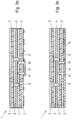
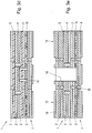
In
In
In einem ersten Verfahrensschritt gemäß
Nach dem Aufbringen und Härten der Kleberschicht 13 erfolgt in dem in
In einem weiteren Verfahrensschritt gemäß
Nachfolgend wird in dem in
Nach der Verbindung zwischen dem starren Bereich 1 der Leiterplatte sowie dem flexiblen Bereich 7 der Leiterplatte über die Verklebung durch die Kleberschichten 15 erfolgt im Bereich der vorab ausgebildeten Fräskanten 14 ausgehend von der von dem flexiblen Bereich 7 abgewandten Stirnfläche des starren Bereichs 1 eine Durchtrennung, wie sie mit 16 angedeutet ist, so daß nunmehr voneinander getrennte Teilbereiche 17 und 18 des ursprünglich einstückigen, starren Bereichs 1 der Leiterplatte über den flexiblen Bereich 7 verbunden sind.After the connection between the rigid region 1 of the printed circuit board and the
Anschließend an die Verbindung zwischen den starren und nunmehr voneinander getrennten Teilbereichen 17 und 18 der Leiterplatte mit dem flexiblen Bereich 7 erfolgt nicht nur ein Vorsehen bzw. Ausbilden von Lötmasken 19 auf den starren Teilbereichen 17 und 18, sondern auch beispielsweise eine Durchkontaktierung zwischen der leitenden Kupferschicht 9 des flexiblen Bereichs 7 der herzustellenden, starr-flexiblen Leiterplatte und einer ersten Kupferschicht 2 der starren Teilbereiche 17 bzw. 18, wie dies bei 20 angedeutet ist.Subsequent to the connection between the rigid and now
Bei der in
In der in
Durch Einhaltung von Temperaturen unter 180 °C, insbesondere zwischen etwa 60 °C und 160 °C, für die Vorhärtung bzw. Vorvernetzung der zweiten Kleberschicht 15 wird darüber hinaus eine entsprechende Vorbereitung für die nachfolgende Verbindung mit dem flexiblen Bereich 7 zur Verfügung gestellt.By maintaining temperatures below 180 ° C, in particular between about 60 ° C and 160 ° C, for the precuring or pre-crosslinking of the second
Anstelle einer Verwendung jeweils eines im wesentlichen identen Klebers für die Kleberschichten 13 und 15 und einer unterschiedlichen Vorbehandlung vor Festlegung des flexiblen Bereichs 7 der Leiterplatte kann naturgemäß auch ein Einsatz von unterschiedlichen Klebern für die Herstellung der Kleberschichten 13 und 15 vorgesehen sein, wobei für eine nachfolgende, einfache Ausbildung einer Durchtrennung 16 in dem starren Bereich 1 der Leiterplatte dafür gesorgt werden soll, daß wie bei dem in
Die Kleberschichten 13 und 15 können hiebei insbesondere abhängig von dem eingesetzten Klebermaterial beispielsweise durch einen Siebdruck, Schablonendruck, ein Streichbeschichten, Walzbeschichten oder Spinbeschichten in einer entsprechend gewünschten, geringen Dicke und mit der erforderlichen Genauigkeit für eine nachfolgende Registrierung bzw. Ausrichtung aufgebracht werden. Durch Einsatz derartiger, an sich bekannter Aufbringungsverfahren, insbesondere Drucktechniken, zur Ausbildung der Kleberschichten kann mit einer entsprechend geringen Schichtstärke, insbesondere weniger als 50 µm, besonders bevorzugt weniger als 40 µm, das Auslangen gefunden werden.The adhesive layers 13 and 15 may in particular be applied depending on the adhesive material used, for example by screen printing, stencil printing, spread coating, roll coating or spin coating in a correspondingly desired, small thickness and with the required accuracy for subsequent registration or alignment. By using such application methods known per se, in particular printing techniques, for the formation of the adhesive layers, the extents can be found with a correspondingly low layer thickness, in particular less than 50 μm, particularly preferably less than 40 μm.
Darüber hinaus ist es durch Vorsehen einer Verklebung zwischen dem starren Bereich 1 bzw. 17 und 18 der Leiterplatte und dem flexiblen Bereich 7 der Leiterplatte möglich, beispielsweise gesetzlich vorgeschriebene Beschränkungen bei der Verwendung bestimmter, gefährlicher Stoffe in Elektro- und Elektronikgeräten in einfacher Weise zu berücksichtigen. Darüber hinaus ist es möglich, einen Kleber mit entsprechend geringem, thermischem Expansionskoeffizienten zu verwenden, wodurch sich die Verarbeitungsschritte weiter vereinfachen lassen.Moreover, by providing a bond between the
Durch die Verwendung einer Verklebung zwischen den starren Teilbereichen 17 und 18 und dem flexiblen Bereich 7 der starr-flexiblen Leiterplatte wird insbesondere unter Berücksichtigung der erzielbaren, geringen Schichtstärke für die Verbindungsschicht und die daraus resultierende Verbesserung der Registriergenauigkeit möglich, Leiterplatten mit flexiblen Lagen für hochkomplexe Bauelemente auch in großen Formaten, beispielsweise im Produktionsformat von HDI-Leiterplatten von mehr als 18 x 24 Zoll, zur Verfügung zu stellen.By using a bond between the
Durch eine Bereitstellung einer entsprechend geringen Schichtstärke durch Vorsehen der Kleberschicht, insbesondere von weniger als 40 µm, ist darüber hinaus eine aktive Flammhemmung nicht erforderlich.By providing a correspondingly low layer thickness by providing the adhesive layer, in particular less than 40 μm, moreover, active flame retardance is not required.
Wie bereits mehrfach ausgeführt, kann mit einfachen Verfahren zur Aufbringung der Kleberschicht bzw. Kleberschichten das Auslangen gefunden werden, wobei derartige Kleberschichten auch entsprechend genau und hochpräzise aufgetragen werden können, so daß zusätzliche Bearbeitungsschritte, beispielsweise Stanzschritte zum Vorbereiten von entsprechenden blattartigen Folien gemäß dem Stand der Technik, entfallen können. Durch die Vereinfachung der Verfahrensführung, insbesondere durch Einsatz von druckfähigen Klebern und dadurch bedingt eine Vereinfachung des Verfahrens, ergeben sich darüber hinaus Möglichkeiten einer Zeit- und Kosteneinsparung bei einer Herstellung einer starr-flexiblen Leiterplatte.As already stated several times, can be found with simple methods for applying the adhesive layer or adhesive layers Auslangen, said adhesive layers can also be applied correspondingly accurate and high precision, so that additional processing steps, such as punching steps for preparing corresponding sheet-like films according to the prior Technology, omitted can. By simplifying the process management, in particular by the use of printable adhesives and thereby a simplification of the process, there are also opportunities for time and cost savings in a production of a rigid-flexible circuit board.
Die in
Claims (11)
- A method for producing a rigid-flexible circuit board, wherein at least one rigid portion or zone (1, 17, 18) of a printed circuit board is connected with at least one flexible portion or zone (7) of a printed circuit board via a layer of non-conductive material or dielectric layer (13, 15), wherein, after having connected the at least one rigid and flexible (7) portion of the circuit board, the rigid portion (1) of the circuit board is divided and a connection between the mutually separated rigid subportions or partial zones (17, 18) of the circuit board is produced via the flexible portion (7) connected therewith, wherein the connection between the at least one rigid portion (1, 17, 18) of the circuit board and the at least one flexible portion (7) of the circuit board is realized by an adhesion (13, 15) prior to dividing the rigid portion, wherein an adhesive layer (13) is applied in the region of the subsequent division of the rigid portion (1) of the circuit board, which adhesive layer is subjected to complete curing, characterized in that adjacent to the partially applied and completely cured adhesive layer (13), a further adhesive layer (15) is applied onto the rigid portion of the circuit board, which further adhesive layer is subsequently only partially cured, and that, after the partial curing of the second or adjacent adhesive layer (15), the rigid portion of the circuit board is connected with the flexible portion of the circuit board via the interposed adhesive layer by the subsequent complete curing of the second adhesive layer (15) and that on the site of the rigid portion (1, 17, 18) of the circuit board, which is to be divided upon application of the flexible portion (7) of the circuit board, and after having applied an adhesive layer (13), milling edges (14) are formed over a partial region of the thickness of the rigid portion (1) of the circuit board in a manner known per se.
- A method according to claim 1, characterized in that, after having fixed the flexible portion (7) of the circuit board to the rigid portion (1) of the circuit board, a division of the rigid portion (1) of the circuit board is effected departing from the surface of the rigid portion (1) of the circuit board that faces away from the formation of the milling edges as far as into the region of the adhesive layer (13) provided between the milling edges (14).
- A method according to claim 1 or 2, characterized in that the adhesion between the rigid and flexible portions (7, 17, 18) of the circuit board is made using a printable adhesive (13, 15).
- A method according to claim 1, 2 or 3, characterized in that the layer thickness of the adhesion (13, 15) is chosen to be smaller than 50µm and, in particular, smaller than 40µm.
- A method according to any one of claims 1 to 4, characterized in that a one- or multi-component thermosetting cross-linking adhesive (13, 15) is used.
- A method according to claim 5, characterized in that the adhesive (13, 15) is selected on the basis of epoxides, polyimides, phenol resins or mixtures thereof, optionally in combination with curing systems based on hydroxyl-, thiol- or amino-functional cross-linking groups.
- A method according to any one of claims 1 to 6, characterized in that the adhesive (13, 15) is provided with inorganic and/or organic fillers.
- A method according to any one of claims 1 to 7, characterized in that the adhesive (13, 15) is applied by screen-printing, stencil-printing, spread-coating, roll-coating or spin-coating.
- A method according to any one of claims 1 to 8, characterized in that the adhesive (13) is selectively applied in the region of the subsequent division of the rigid portion (1) of the circuit board for the formation of the separate rigid subportions (17, 18).
- A method according to any of the claims 1 to 9, characterized in that the precuring and pre-cross-linking of the second adhesive layer (15) is carried out at temperatures of below 180°C and, in particular, between about 60°C and 160°C.
- A method according to any one of claims 1 to 10, characterized in that a multilayer circuit board is at least used for the rigid portion (1, 17, 18) of the circuit board.
Applications Claiming Priority (2)
| Application Number | Priority Date | Filing Date | Title |
|---|---|---|---|
| AT0009907U AT10029U1 (en) | 2007-02-16 | 2007-02-16 | METHOD FOR PRODUCING A RIGID FLEXIBLE PCB AND RIGID FLEXIBLE PCB |
| PCT/AT2008/000030 WO2008098272A1 (en) | 2007-02-16 | 2008-01-30 | Method for producing a flexi-rigid printed circuit board and flexi-rigid printed circuit board |
Publications (2)
| Publication Number | Publication Date |
|---|---|
| EP2119330A1 EP2119330A1 (en) | 2009-11-18 |
| EP2119330B1 true EP2119330B1 (en) | 2017-07-19 |
Family
ID=39367422
Family Applications (1)
| Application Number | Title | Priority Date | Filing Date |
|---|---|---|---|
| EP08700296.0A Not-in-force EP2119330B1 (en) | 2007-02-16 | 2008-01-30 | Method for producing a flexi-rigid printed circuit board |
Country Status (7)
| Country | Link |
|---|---|
| US (1) | US8500938B2 (en) |
| EP (1) | EP2119330B1 (en) |
| JP (1) | JP5327545B2 (en) |
| KR (1) | KR20090109109A (en) |
| CN (1) | CN101658082B (en) |
| AT (1) | AT10029U1 (en) |
| WO (1) | WO2008098272A1 (en) |
Families Citing this family (25)
| Publication number | Priority date | Publication date | Assignee | Title |
|---|---|---|---|---|
| WO2010007704A1 (en) * | 2008-07-16 | 2010-01-21 | イビデン株式会社 | Flex-rigid wiring board and electronic device |
| AT12321U1 (en) | 2009-01-09 | 2012-03-15 | Austria Tech & System Tech | MULTILAYER PCB LAYER ELEMENT WITH AT LEAST ONE LASER BEAM STOPPING ELEMENT AND METHOD FOR ATTACHING SUCH A LASER BEAM STOPPER IN A MULTILAYER PCB ELEMENT |
| DE102010045536B4 (en) * | 2010-09-15 | 2012-06-21 | Trw Automotive Electronics & Components Gmbh | Electrodynamic actuator |
| AT12737U1 (en) * | 2010-09-17 | 2012-10-15 | Austria Tech & System Tech | METHOD FOR PRODUCING A CONDUCTOR PLATE COMPOSED OF MULTIPLE PCB SURFACES AND PCB |
| US20120325524A1 (en) * | 2011-06-23 | 2012-12-27 | Ibiden Co., Ltd. | Flex-rigid wiring board and method for manufacturing the same |
| CN103096647B (en) * | 2011-10-31 | 2016-01-13 | 健鼎(无锡)电子有限公司 | The manufacture method of folding type printed circuit board (PCB) |
| CN102802361B (en) * | 2012-08-27 | 2014-12-10 | 皆利士多层线路版(中山)有限公司 | Making method of semi-flexible printed circuit board |
| TWI477212B (en) * | 2013-01-24 | 2015-03-11 | Unimicron Technology Corp | Rigid and flexible composite circuit board and manufacturing metodh thereof |
| CN103987207B (en) * | 2013-02-07 | 2017-03-01 | 欣兴电子股份有限公司 | Flexible and hard composite circuit board and manufacturing method thereof |
| WO2014207822A1 (en) * | 2013-06-25 | 2014-12-31 | 株式会社メイコー | Printed wiring board |
| TWI501713B (en) * | 2013-08-26 | 2015-09-21 | Unimicron Technology Corp | Rigid flex module and manufacturing method for the same |
| CN104582325B (en) * | 2013-10-12 | 2018-03-27 | 鹏鼎控股(深圳)股份有限公司 | Rigid-flex combined board and preparation method thereof, circuit board module |
| CN103578804B (en) * | 2013-11-01 | 2015-11-18 | 电子科技大学 | A kind of preparation method of rigid/flexible combined printed circuit board |
| CN105282995B (en) * | 2014-06-24 | 2018-04-06 | 健鼎(无锡)电子有限公司 | The method for removing the multilayer wiring structure of part |
| US9997442B1 (en) | 2016-12-14 | 2018-06-12 | Advanced Semiconductor Engineering, Inc. | Semiconductor device and method of manufacturing the same |
| KR102327991B1 (en) * | 2016-12-16 | 2021-11-18 | 삼성디스플레이 주식회사 | Method of manufacturing display apparatus |
| CN108243568A (en) * | 2016-12-27 | 2018-07-03 | 健鼎(无锡)电子有限公司 | The production method of flexible circuit board |
| CN206602182U (en) * | 2017-04-06 | 2017-10-31 | 京东方科技集团股份有限公司 | A kind of antenna structure and communication apparatus |
| CN107328536B (en) * | 2017-08-16 | 2023-07-25 | 拓旷(上海)光电科技有限公司 | Test machine |
| US10420208B2 (en) * | 2017-09-06 | 2019-09-17 | Microsoft Technology Licensing, Llc | Metal layering construction in flex/rigid-flex printed circuits |
| CN117061847A (en) | 2017-11-03 | 2023-11-14 | Zf主动安全和电子美国有限公司 | Driver assistance system |
| US20200053887A1 (en) | 2018-08-09 | 2020-02-13 | At&S Austria Technologie & Systemtechnik Aktiengesellschaft | Mechanically Robust Component Carrier With Rigid and Flexible Portions |
| CN209572202U (en) | 2018-10-31 | 2019-11-01 | 奥特斯(中国)有限公司 | Component load-bearing part semi-flexible |
| KR102268389B1 (en) * | 2019-09-11 | 2021-06-23 | 삼성전기주식회사 | Printed circuit board and antenna module comprising the same |
| CN112582386B (en) * | 2019-09-27 | 2022-05-27 | 珠海格力电器股份有限公司 | Power module, preparation method thereof and electrical equipment |
Citations (1)
| Publication number | Priority date | Publication date | Assignee | Title |
|---|---|---|---|---|
| JPH1022645A (en) * | 1996-07-08 | 1998-01-23 | Nippon Avionics Co Ltd | Manufacture of printed wiring board with cavity |
Family Cites Families (13)
| Publication number | Priority date | Publication date | Assignee | Title |
|---|---|---|---|---|
| US4931134A (en) * | 1989-08-15 | 1990-06-05 | Parlex Corporation | Method of using laser routing to form a rigid/flex circuit board |
| US5004639A (en) * | 1990-01-23 | 1991-04-02 | Sheldahl, Inc. | Rigid flex printed circuit configuration |
| DE4003344C1 (en) * | 1990-02-05 | 1991-06-13 | Fa. Carl Freudenberg, 6940 Weinheim, De | |
| DE4003345C1 (en) * | 1990-02-05 | 1991-08-08 | Fa. Carl Freudenberg, 6940 Weinheim, De | |
| JP3209772B2 (en) * | 1991-07-08 | 2001-09-17 | 株式会社フジクラ | Manufacturing method of rigid flex wiring board |
| JP3310037B2 (en) * | 1993-01-05 | 2002-07-29 | 株式会社東芝 | Manufacturing method of printed wiring board |
| JPH06252552A (en) * | 1993-02-26 | 1994-09-09 | Hitachi Chem Co Ltd | Manufacture of wiring board |
| JPH10173342A (en) * | 1996-12-13 | 1998-06-26 | Toshiba Chem Corp | Multilayer flexible rigid wiring board and production thereof |
| JP2003332742A (en) * | 2002-05-16 | 2003-11-21 | Kyocera Chemical Corp | Multilayer flex-rigid wiring board and its manufacturing method |
| DE10243637B4 (en) * | 2002-09-19 | 2007-04-26 | Ruwel Ag | Printed circuit board with at least one rigid and at least one flexible region and method for producing rigid-flexible printed circuit boards |
| DE20221189U1 (en) | 2002-09-19 | 2005-05-19 | Ruwel Ag | Printed circuit board with at least one rigid area and at least one flexible area |
| DE20221121U1 (en) * | 2002-09-19 | 2005-03-24 | Ruwel Ag | Circuit board comprises at least one rigid region and one flexible region, a copper coating on the rigid layer, and an adhesive |
| DE10349963A1 (en) * | 2003-10-24 | 2005-06-02 | Leonhard Kurz Gmbh & Co. Kg | Process for producing a film |
-
2007
- 2007-02-16 AT AT0009907U patent/AT10029U1/en not_active IP Right Cessation
-
2008
- 2008-01-30 JP JP2009549743A patent/JP5327545B2/en not_active Expired - Fee Related
- 2008-01-30 KR KR1020097017101A patent/KR20090109109A/en not_active Application Discontinuation
- 2008-01-30 WO PCT/AT2008/000030 patent/WO2008098272A1/en active Search and Examination
- 2008-01-30 CN CN2008800117111A patent/CN101658082B/en not_active Expired - Fee Related
- 2008-01-30 US US12/449,608 patent/US8500938B2/en active Active
- 2008-01-30 EP EP08700296.0A patent/EP2119330B1/en not_active Not-in-force
Patent Citations (1)
| Publication number | Priority date | Publication date | Assignee | Title |
|---|---|---|---|---|
| JPH1022645A (en) * | 1996-07-08 | 1998-01-23 | Nippon Avionics Co Ltd | Manufacture of printed wiring board with cavity |
Also Published As
| Publication number | Publication date |
|---|---|
| JP5327545B2 (en) | 2013-10-30 |
| AT10029U1 (en) | 2008-07-15 |
| CN101658082A (en) | 2010-02-24 |
| JP2010518649A (en) | 2010-05-27 |
| CN101658082B (en) | 2013-01-02 |
| US8500938B2 (en) | 2013-08-06 |
| EP2119330A1 (en) | 2009-11-18 |
| WO2008098272A8 (en) | 2008-11-27 |
| KR20090109109A (en) | 2009-10-19 |
| WO2008098272A1 (en) | 2008-08-21 |
| US20100025086A1 (en) | 2010-02-04 |
Similar Documents
| Publication | Publication Date | Title |
|---|---|---|
| EP2119330B1 (en) | Method for producing a flexi-rigid printed circuit board | |
| EP2342958B1 (en) | Method for integrating an electronic component into a printed circuit board | |
| EP2286644B1 (en) | Method for integrating at least one electronic component into a printed circuit board, and printed circuit board | |
| DE69934674T2 (en) | METHOD FOR THE PRODUCTION OF MULTIFUNCTIONAL MICROWAVE MODULES FROM FLUOROPOLYMIC COMPOSITE SUBSTRATES | |
| DE4006063C2 (en) | Process for the production of a printed circuit board | |
| EP2119327B1 (en) | Method for removing a part of a planar material layer | |
| EP2668835B1 (en) | Method for integrating an electronic component into a printed circuit board or a printed circuit board intermediate product | |
| EP2868170B1 (en) | Method for embedding at least one component into a printed circuit board | |
| EP2452546A1 (en) | Method for producing a printed circuit board consisting of at least two printed circuit board regions, and printed circuit board | |
| EP2818032B1 (en) | Method for producing a circuit board and use of such a method | |
| WO2007087660A1 (en) | Printed circuit board element having at least one component embedded therein and method for embedding at least one component in a printed circuit board element | |
| WO2008098270A1 (en) | Method for producing a flexi-rigid printed circuit board and flexi-rigid printed circuit board | |
| EP0167051A1 (en) | Thermostable and irradiation-curable polymer system based on bisphenol and epichlorohydrine, and method for its preparation | |
| DE4206746C1 (en) | Manufacture of circuit board with rigid and flexible sections - has flexible sections created by having non-bonding insert of insulation broken away | |
| DE60124665T2 (en) | MANUFACTURING PROCESS FOR A PCB | |
| WO2007131256A2 (en) | Method for fixing an electronic component on a printed circuit board and system comprising a printed circuit board and at least one electronic component | |
| EP2467003A2 (en) | Circuit board and method for producing circuit boards | |
| DE102020111996A1 (en) | Process for the production of a printed circuit board and printed circuit board with at least one embedded electronic component | |
| DE10205592B4 (en) | Method for producing a semifinished product for printed circuit boards | |
| DE10248112B4 (en) | Process for the production of printed electrical circuits | |
| EP1093909B1 (en) | Composite film | |
| AT399250B (en) | MULTILAYER CIRCUIT BOARD AND METHOD FOR THEIR PRODUCTION | |
| DE69836685T2 (en) | SWITCHING PART AND PCB | |
| DE102016219732A1 (en) | Method for producing a multilayer printed circuit board | |
| DE102021112814A1 (en) | Process for manufacturing a printed circuit board and printed circuit board with at least one embedded electronic component |
Legal Events
| Date | Code | Title | Description |
|---|---|---|---|
| PUAI | Public reference made under article 153(3) epc to a published international application that has entered the european phase |
Free format text: ORIGINAL CODE: 0009012 |
|
| 17P | Request for examination filed |
Effective date: 20090831 |
|
| AK | Designated contracting states |
Kind code of ref document: A1 Designated state(s): AT BE BG CH CY CZ DE DK EE ES FI FR GB GR HR HU IE IS IT LI LT LU LV MC MT NL NO PL PT RO SE SI SK TR |
|
| DAX | Request for extension of the european patent (deleted) | ||
| 17Q | First examination report despatched |
Effective date: 20130409 |
|
| GRAP | Despatch of communication of intention to grant a patent |
Free format text: ORIGINAL CODE: EPIDOSNIGR1 |
|
| INTG | Intention to grant announced |
Effective date: 20170215 |
|
| GRAS | Grant fee paid |
Free format text: ORIGINAL CODE: EPIDOSNIGR3 |
|
| GRAA | (expected) grant |
Free format text: ORIGINAL CODE: 0009210 |
|
| AK | Designated contracting states |
Kind code of ref document: B1 Designated state(s): AT BE BG CH CY CZ DE DK EE ES FI FR GB GR HR HU IE IS IT LI LT LU LV MC MT NL NO PL PT RO SE SI SK TR |
|
| REG | Reference to a national code |
Ref country code: GB Ref legal event code: FG4D Free format text: NOT ENGLISH |
|
| REG | Reference to a national code |
Ref country code: CH Ref legal event code: EP |
|
| REG | Reference to a national code |
Ref country code: IE Ref legal event code: FG4D Free format text: LANGUAGE OF EP DOCUMENT: GERMAN |
|
| REG | Reference to a national code |
Ref country code: AT Ref legal event code: REF Ref document number: 911599 Country of ref document: AT Kind code of ref document: T Effective date: 20170815 |
|
| REG | Reference to a national code |
Ref country code: DE Ref legal event code: R096 Ref document number: 502008015470 Country of ref document: DE |
|
| REG | Reference to a national code |
Ref country code: NL Ref legal event code: MP Effective date: 20170719 |
|
| REG | Reference to a national code |
Ref country code: LT Ref legal event code: MG4D |
|
| PG25 | Lapsed in a contracting state [announced via postgrant information from national office to epo] |
Ref country code: NO Free format text: LAPSE BECAUSE OF FAILURE TO SUBMIT A TRANSLATION OF THE DESCRIPTION OR TO PAY THE FEE WITHIN THE PRESCRIBED TIME-LIMIT Effective date: 20171019 Ref country code: LT Free format text: LAPSE BECAUSE OF FAILURE TO SUBMIT A TRANSLATION OF THE DESCRIPTION OR TO PAY THE FEE WITHIN THE PRESCRIBED TIME-LIMIT Effective date: 20170719 Ref country code: FI Free format text: LAPSE BECAUSE OF FAILURE TO SUBMIT A TRANSLATION OF THE DESCRIPTION OR TO PAY THE FEE WITHIN THE PRESCRIBED TIME-LIMIT Effective date: 20170719 Ref country code: HR Free format text: LAPSE BECAUSE OF FAILURE TO SUBMIT A TRANSLATION OF THE DESCRIPTION OR TO PAY THE FEE WITHIN THE PRESCRIBED TIME-LIMIT Effective date: 20170719 Ref country code: NL Free format text: LAPSE BECAUSE OF FAILURE TO SUBMIT A TRANSLATION OF THE DESCRIPTION OR TO PAY THE FEE WITHIN THE PRESCRIBED TIME-LIMIT Effective date: 20170719 Ref country code: SE Free format text: LAPSE BECAUSE OF FAILURE TO SUBMIT A TRANSLATION OF THE DESCRIPTION OR TO PAY THE FEE WITHIN THE PRESCRIBED TIME-LIMIT Effective date: 20170719 |
|
| PG25 | Lapsed in a contracting state [announced via postgrant information from national office to epo] |
Ref country code: LV Free format text: LAPSE BECAUSE OF FAILURE TO SUBMIT A TRANSLATION OF THE DESCRIPTION OR TO PAY THE FEE WITHIN THE PRESCRIBED TIME-LIMIT Effective date: 20170719 Ref country code: GR Free format text: LAPSE BECAUSE OF FAILURE TO SUBMIT A TRANSLATION OF THE DESCRIPTION OR TO PAY THE FEE WITHIN THE PRESCRIBED TIME-LIMIT Effective date: 20171020 Ref country code: BG Free format text: LAPSE BECAUSE OF FAILURE TO SUBMIT A TRANSLATION OF THE DESCRIPTION OR TO PAY THE FEE WITHIN THE PRESCRIBED TIME-LIMIT Effective date: 20171019 Ref country code: ES Free format text: LAPSE BECAUSE OF FAILURE TO SUBMIT A TRANSLATION OF THE DESCRIPTION OR TO PAY THE FEE WITHIN THE PRESCRIBED TIME-LIMIT Effective date: 20170719 Ref country code: PL Free format text: LAPSE BECAUSE OF FAILURE TO SUBMIT A TRANSLATION OF THE DESCRIPTION OR TO PAY THE FEE WITHIN THE PRESCRIBED TIME-LIMIT Effective date: 20170719 Ref country code: IS Free format text: LAPSE BECAUSE OF FAILURE TO SUBMIT A TRANSLATION OF THE DESCRIPTION OR TO PAY THE FEE WITHIN THE PRESCRIBED TIME-LIMIT Effective date: 20171119 |
|
| REG | Reference to a national code |
Ref country code: DE Ref legal event code: R097 Ref document number: 502008015470 Country of ref document: DE |
|
| PG25 | Lapsed in a contracting state [announced via postgrant information from national office to epo] |
Ref country code: CZ Free format text: LAPSE BECAUSE OF FAILURE TO SUBMIT A TRANSLATION OF THE DESCRIPTION OR TO PAY THE FEE WITHIN THE PRESCRIBED TIME-LIMIT Effective date: 20170719 Ref country code: RO Free format text: LAPSE BECAUSE OF FAILURE TO SUBMIT A TRANSLATION OF THE DESCRIPTION OR TO PAY THE FEE WITHIN THE PRESCRIBED TIME-LIMIT Effective date: 20170719 Ref country code: DK Free format text: LAPSE BECAUSE OF FAILURE TO SUBMIT A TRANSLATION OF THE DESCRIPTION OR TO PAY THE FEE WITHIN THE PRESCRIBED TIME-LIMIT Effective date: 20170719 |
|
| PLBE | No opposition filed within time limit |
Free format text: ORIGINAL CODE: 0009261 |
|
| STAA | Information on the status of an ep patent application or granted ep patent |
Free format text: STATUS: NO OPPOSITION FILED WITHIN TIME LIMIT |
|
| PG25 | Lapsed in a contracting state [announced via postgrant information from national office to epo] |
Ref country code: SK Free format text: LAPSE BECAUSE OF FAILURE TO SUBMIT A TRANSLATION OF THE DESCRIPTION OR TO PAY THE FEE WITHIN THE PRESCRIBED TIME-LIMIT Effective date: 20170719 Ref country code: IT Free format text: LAPSE BECAUSE OF FAILURE TO SUBMIT A TRANSLATION OF THE DESCRIPTION OR TO PAY THE FEE WITHIN THE PRESCRIBED TIME-LIMIT Effective date: 20170719 Ref country code: EE Free format text: LAPSE BECAUSE OF FAILURE TO SUBMIT A TRANSLATION OF THE DESCRIPTION OR TO PAY THE FEE WITHIN THE PRESCRIBED TIME-LIMIT Effective date: 20170719 |
|
| 26N | No opposition filed |
Effective date: 20180420 |
|
| PG25 | Lapsed in a contracting state [announced via postgrant information from national office to epo] |
Ref country code: SI Free format text: LAPSE BECAUSE OF FAILURE TO SUBMIT A TRANSLATION OF THE DESCRIPTION OR TO PAY THE FEE WITHIN THE PRESCRIBED TIME-LIMIT Effective date: 20170719 |
|
| REG | Reference to a national code |
Ref country code: CH Ref legal event code: PL |
|
| PG25 | Lapsed in a contracting state [announced via postgrant information from national office to epo] |
Ref country code: MT Free format text: LAPSE BECAUSE OF FAILURE TO SUBMIT A TRANSLATION OF THE DESCRIPTION OR TO PAY THE FEE WITHIN THE PRESCRIBED TIME-LIMIT Effective date: 20170719 |
|
| PG25 | Lapsed in a contracting state [announced via postgrant information from national office to epo] |
Ref country code: LU Free format text: LAPSE BECAUSE OF NON-PAYMENT OF DUE FEES Effective date: 20180130 Ref country code: FR Free format text: LAPSE BECAUSE OF NON-PAYMENT OF DUE FEES Effective date: 20180131 |
|
| REG | Reference to a national code |
Ref country code: IE Ref legal event code: MM4A |
|
| REG | Reference to a national code |
Ref country code: FR Ref legal event code: ST Effective date: 20180928 |
|
| REG | Reference to a national code |
Ref country code: BE Ref legal event code: MM Effective date: 20180131 |
|
| PG25 | Lapsed in a contracting state [announced via postgrant information from national office to epo] |
Ref country code: LI Free format text: LAPSE BECAUSE OF NON-PAYMENT OF DUE FEES Effective date: 20180131 Ref country code: BE Free format text: LAPSE BECAUSE OF NON-PAYMENT OF DUE FEES Effective date: 20180131 Ref country code: CH Free format text: LAPSE BECAUSE OF NON-PAYMENT OF DUE FEES Effective date: 20180131 |
|
| PG25 | Lapsed in a contracting state [announced via postgrant information from national office to epo] |
Ref country code: IE Free format text: LAPSE BECAUSE OF NON-PAYMENT OF DUE FEES Effective date: 20180130 |
|
| REG | Reference to a national code |
Ref country code: AT Ref legal event code: MM01 Ref document number: 911599 Country of ref document: AT Kind code of ref document: T Effective date: 20180130 |
|
| PG25 | Lapsed in a contracting state [announced via postgrant information from national office to epo] |
Ref country code: AT Free format text: LAPSE BECAUSE OF NON-PAYMENT OF DUE FEES Effective date: 20180130 |
|
| PG25 | Lapsed in a contracting state [announced via postgrant information from national office to epo] |
Ref country code: MC Free format text: LAPSE BECAUSE OF FAILURE TO SUBMIT A TRANSLATION OF THE DESCRIPTION OR TO PAY THE FEE WITHIN THE PRESCRIBED TIME-LIMIT Effective date: 20170719 |
|
| PG25 | Lapsed in a contracting state [announced via postgrant information from national office to epo] |
Ref country code: TR Free format text: LAPSE BECAUSE OF FAILURE TO SUBMIT A TRANSLATION OF THE DESCRIPTION OR TO PAY THE FEE WITHIN THE PRESCRIBED TIME-LIMIT Effective date: 20170719 |
|
| PG25 | Lapsed in a contracting state [announced via postgrant information from national office to epo] |
Ref country code: PT Free format text: LAPSE BECAUSE OF FAILURE TO SUBMIT A TRANSLATION OF THE DESCRIPTION OR TO PAY THE FEE WITHIN THE PRESCRIBED TIME-LIMIT Effective date: 20170719 Ref country code: HU Free format text: LAPSE BECAUSE OF FAILURE TO SUBMIT A TRANSLATION OF THE DESCRIPTION OR TO PAY THE FEE WITHIN THE PRESCRIBED TIME-LIMIT; INVALID AB INITIO Effective date: 20080130 |
|
| PG25 | Lapsed in a contracting state [announced via postgrant information from national office to epo] |
Ref country code: CY Free format text: LAPSE BECAUSE OF FAILURE TO SUBMIT A TRANSLATION OF THE DESCRIPTION OR TO PAY THE FEE WITHIN THE PRESCRIBED TIME-LIMIT Effective date: 20170719 |
|
| PGFP | Annual fee paid to national office [announced via postgrant information from national office to epo] |
Ref country code: DE Payment date: 20201221 Year of fee payment: 14 Ref country code: GB Payment date: 20210114 Year of fee payment: 14 |
|
| REG | Reference to a national code |
Ref country code: DE Ref legal event code: R119 Ref document number: 502008015470 Country of ref document: DE |
|
| GBPC | Gb: european patent ceased through non-payment of renewal fee |
Effective date: 20220130 |
|
| PG25 | Lapsed in a contracting state [announced via postgrant information from national office to epo] |
Ref country code: GB Free format text: LAPSE BECAUSE OF NON-PAYMENT OF DUE FEES Effective date: 20220130 Ref country code: DE Free format text: LAPSE BECAUSE OF NON-PAYMENT OF DUE FEES Effective date: 20220802 |
|
| P01 | Opt-out of the competence of the unified patent court (upc) registered |
Effective date: 20230526 |