EP2118754B1 - Vorrichtung und verfahren zur reduzierung von ausfällen in einer mehrstufigen cache-hierarchie - Google Patents
Vorrichtung und verfahren zur reduzierung von ausfällen in einer mehrstufigen cache-hierarchie Download PDFInfo
- Publication number
- EP2118754B1 EP2118754B1 EP08728594.6A EP08728594A EP2118754B1 EP 2118754 B1 EP2118754 B1 EP 2118754B1 EP 08728594 A EP08728594 A EP 08728594A EP 2118754 B1 EP2118754 B1 EP 2118754B1
- Authority
- EP
- European Patent Office
- Prior art keywords
- cache
- line
- level cache
- higher level
- next higher
- Prior art date
- Legal status (The legal status is an assumption and is not a legal conclusion. Google has not performed a legal analysis and makes no representation as to the accuracy of the status listed.)
- Not-in-force
Links
Images


Classifications
-
- G—PHYSICS
- G06—COMPUTING; CALCULATING OR COUNTING
- G06F—ELECTRIC DIGITAL DATA PROCESSING
- G06F12/00—Accessing, addressing or allocating within memory systems or architectures
- G06F12/02—Addressing or allocation; Relocation
- G06F12/08—Addressing or allocation; Relocation in hierarchically structured memory systems, e.g. virtual memory systems
- G06F12/0802—Addressing of a memory level in which the access to the desired data or data block requires associative addressing means, e.g. caches
- G06F12/0893—Caches characterised by their organisation or structure
- G06F12/0897—Caches characterised by their organisation or structure with two or more cache hierarchy levels
-
- G—PHYSICS
- G06—COMPUTING; CALCULATING OR COUNTING
- G06F—ELECTRIC DIGITAL DATA PROCESSING
- G06F12/00—Accessing, addressing or allocating within memory systems or architectures
- G06F12/02—Addressing or allocation; Relocation
- G06F12/08—Addressing or allocation; Relocation in hierarchically structured memory systems, e.g. virtual memory systems
-
- G—PHYSICS
- G06—COMPUTING; CALCULATING OR COUNTING
- G06F—ELECTRIC DIGITAL DATA PROCESSING
- G06F12/00—Accessing, addressing or allocating within memory systems or architectures
-
- G—PHYSICS
- G06—COMPUTING; CALCULATING OR COUNTING
- G06F—ELECTRIC DIGITAL DATA PROCESSING
- G06F12/00—Accessing, addressing or allocating within memory systems or architectures
- G06F12/02—Addressing or allocation; Relocation
- G06F12/08—Addressing or allocation; Relocation in hierarchically structured memory systems, e.g. virtual memory systems
- G06F12/12—Replacement control
- G06F12/121—Replacement control using replacement algorithms
- G06F12/128—Replacement control using replacement algorithms adapted to multidimensional cache systems, e.g. set-associative, multicache, multiset or multilevel
-
- G—PHYSICS
- G06—COMPUTING; CALCULATING OR COUNTING
- G06F—ELECTRIC DIGITAL DATA PROCESSING
- G06F12/00—Accessing, addressing or allocating within memory systems or architectures
- G06F12/02—Addressing or allocation; Relocation
- G06F12/08—Addressing or allocation; Relocation in hierarchically structured memory systems, e.g. virtual memory systems
- G06F12/0802—Addressing of a memory level in which the access to the desired data or data block requires associative addressing means, e.g. caches
- G06F12/0804—Addressing of a memory level in which the access to the desired data or data block requires associative addressing means, e.g. caches with main memory updating
-
- G—PHYSICS
- G06—COMPUTING; CALCULATING OR COUNTING
- G06F—ELECTRIC DIGITAL DATA PROCESSING
- G06F2212/00—Indexing scheme relating to accessing, addressing or allocation within memory systems or architectures
- G06F2212/10—Providing a specific technical effect
- G06F2212/1028—Power efficiency
-
- Y—GENERAL TAGGING OF NEW TECHNOLOGICAL DEVELOPMENTS; GENERAL TAGGING OF CROSS-SECTIONAL TECHNOLOGIES SPANNING OVER SEVERAL SECTIONS OF THE IPC; TECHNICAL SUBJECTS COVERED BY FORMER USPC CROSS-REFERENCE ART COLLECTIONS [XRACs] AND DIGESTS
- Y02—TECHNOLOGIES OR APPLICATIONS FOR MITIGATION OR ADAPTATION AGAINST CLIMATE CHANGE
- Y02D—CLIMATE CHANGE MITIGATION TECHNOLOGIES IN INFORMATION AND COMMUNICATION TECHNOLOGIES [ICT], I.E. INFORMATION AND COMMUNICATION TECHNOLOGIES AIMING AT THE REDUCTION OF THEIR OWN ENERGY USE
- Y02D10/00—Energy efficient computing, e.g. low power processors, power management or thermal management
Definitions
- the present disclosure relates generally to the field of cache memory and, more specifically, to memory systems with instruction, data, and victim caches.
- the processing system for such products includes a processor and memory complex for storing instructions and data.
- Large capacity main memory commonly has slow access times as compared to the processor cycle time.
- the memory complex is conventionally organized in a hierarchy based on capacity and performance of cache memories, with the highest performance and lowest capacity cache located closest to the processor. For example, a level 1 instruction cache and a level 1 data cache would generally be directly attached to the processor. While a level 2 unified cache is connected to the level 1 (L1) instruction and data caches. Further, a system memory is connected to the level 2 (L2) unified cache.
- the level 1 instruction cache commonly operates at the processor speed and the level 2 unified cache operates slower than the level 1 cache, but has a faster access time than that of the system memory.
- Alternative memory organizations abound, for example, memory hierarchies having a level 3 cache in addition to an L1 and an L2 cache. Another memory organization may use only a level 1 cache and a system memory.
- a memory organization may be made up of a hierarchy of caches operating as inclusive caches, strictly inclusive caches, exclusive caches, or a combination of these cache types.
- any two levels of cache that are exclusive to each other can not contain the same cache line.
- Any two levels of cache that are inclusive of each other may contain the same cache line.
- Any two levels of cache that are strictly inclusive of each other means that the larger cache, usually a higher level cache, must contain all lines that are in the smaller cache, usually a lower level cache.
- any two or more cache levels may operate as one type of cache, such as exclusive, and the remaining cache levels may operate as one of the alternative types of cache, such as inclusive.
- An instruction cache is generally constructed to support a plurality of instructions located at a single address in the instruction cache.
- a data cache is generally constructed to support a plurality of data units located at a single address in the data cache, where a data unit may be a variable number of bytes depending on the processor.
- This plurality of instructions or data units is generally called a cache line or simply a line. For example, a processor fetches an instruction or a data unit from an L1 cache and if the instruction or data unit is present in the cache a "hit" occurs and the instruction or data unit is provided to the processor. If the instruction or data unit is not present in the L1 cache a "miss" occurs. A miss may occur on an instruction or data unit access anywhere in a cache line.
- a replacement policy is used to determine which cache line to replace. For example, selecting or victimizing a cache line that has been used the least represents a least recently used (LRU) policy.
- LRU least recently used
- a cache line may also have associated with it a number of status bits, such as a valid bit and a dirty bit.
- the valid bit indicates that instructions or data reside in the cache line.
- the dirty bit indicates whether a modification to the cache line has occurred. In a write-back cache, the dirty bit indicates that when a cache line is to be replaced the modifications need to be written back to the next higher memory level in the memory system hierarchy.
- a victim cache may be a separate buffer connected to a cache, such as a level 1 cache, or integrated in an adjacent higher level cache.
- Victim cache lines may be allocated in the victim cache under the assumptions that a victim line may be needed relatively shortly after being evicted and that accessing the victim line when needed from a victim cache is faster than accessing the victim line from a higher level of the memory hierarchy.
- a castout occurs when a line is displaced from the lower level cache and is allocated in the higher level cache, thus caching the lower level cache's victims.
- the lower level cache sends all displaced lines, both dirty and non-dirty, to the higher level cache.
- the victim line may already exist in the victim cache and rewriting already existing lines wastes power and reduces bandwidth to the victim cache.
- US 5,564,035 describes a multi-level memory system having a primary cache and a secondary cache in which unnecessary swapping operations are minimized.
- a tracking method to reduce allocation of displaced cache lines is provided in accordance with claim 1; and a memory system having a plurality of cache levels is provided in accordance with claim 11.
- the present disclosure recognizes that reducing power requirements in a memory system is important to portable applications and in general for reducing power needs in processing systems.
- an embodiment of the invention addresses a tracking method to reduce allocation of displaced cache lines.
- a line is selected to be displaced in a lower level cache.
- Information associated with the selected line is identified which indicates that the selected line is present in a higher level cache.
- An allocation of the selected line in the higher level cache is prevented based on the identified information. Preventing an allocation of the selected line saves power that would be associated with the allocation.
- Another embodiment of the invention addresses a method to reduce castouts.
- allocation information is saved in the level X cache in a tag of a cache line associated with the miss.
- the allocation information indicates whether the cache line was allocated in a level X+1 cache.
- a line is selected to be replaced in the level X cache.
- a castout of the selected line from the level X cache to the level X+1 cache is prevented in response to the allocation information of the selected line indicating the cache line was allocated in the level X+1 cache.
- a lower level cache is configured to store a plurality of first cache lines each with an allocation bit.
- the allocation bit associated with one of the plurality of first cache lines indicates whether the one of the plurality of first cache lines was allocated in a higher level cache.
- a castout logic circuit is configured to determine whether a first cache line selected for displacement from the plurality of first cache lines is a cache line that is redundant with a cache line in the higher level cache based on the allocation bit associated with the selected first cache line. A castout of the selected first cache line to the higher level cache is prevented in response to the allocation bit of the selected first cache line.
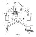
- FIG. 1 illustrates a wireless communication system
- FIG. 2 is a functional block diagram of an exemplary processor and memory complex in which castouts are reduced.
- FIG. 3 is a flow diagram illustrating a process for reducing castouts.
- FIG. 1 illustrates an exemplary wireless communication system 100 in which an embodiment of the invention may be advantageously employed.
- FIG. 1 shows three remote units 120, 130, and 150 and two base stations 140. It will be recognized that common wireless communication systems may have many more remote units and base stations.
- Remote units 120, 130, and 150 include hardware components, software components, or both as represented by components 125A, 125C, and 125B, respectively, which have been adapted to embody the invention as discussed further below.
- FIG. 1 shows forward link signals 180 from the base stations 140 to the remote units 120, 130, and 150 and reverse link signals 190 from the remote units 120, 130, and 150 to the base stations 140.
- remote unit 120 is shown as a mobile telephone
- remote unit 130 is shown as a portable computer
- remote unit 150 is shown as a fixed location remote unit in a wireless local loop system.
- the remote units may alternatively be cell phones, pagers, walkie talkies, handheld personal communication systems (PCS) units, portable data units such as personal data assistants, or fixed location data units such as meter reading equipment.
- FIG. 1 illustrates remote units according to the teachings of the disclosure, the disclosure is not limited to these exemplary illustrated units.
- Embodiments of the invention may be suitably employed in any device having a processor with at least two levels of a memory hierarchy, such as a level 1 cache and a level 2 cache.
- FIG. 2 is a functional block diagram of an exemplary processor and memory complex 200 in which castouts are reduced.
- the exemplary processor and memory complex 200 includes a processor 202, a level 1 cache (L1 cache) 203 comprising an L1 cache line array 204 and an L1 cache control unit 206, an inclusive level 2 cache (L2 cache) 208, and a system memory 210.
- the L1 cache control unit 206 includes castout logic circuit 212 and a level 1 content addressable memory (L1 CAM) 214 for tag matching, as may be used in various types of caches, such as, a set associative cache or a fully associative cache. Peripheral devices, which may connect to the processor complex, are not shown for clarity of discussion.
- the exemplary processor and memory complex 200 may be suitably employed in various embodiments of the invention in components 125A-C for executing program code that is stored in the caches 203 and 208 and the system memory 210.
- the L1 cache line array 204 may include a plurality of lines, such as cache lines 215 - 217.
- the L1 cache 203 is a data cache with each line made up of a plurality of data units.
- the L1 cache 203 is an instruction cache with each line made up of a plurality of instructions.
- the L1 cache 203 is a unified cache with each line made up of a plurality of instructions or data units. For example, each line is made up of a plurality of elements (U0, U1, ..., U7) 218-225, respectively, appropriate for the instantiated cache embodiment.
- the cache lines 215 - 217 reside in the L1 cache line array 204 at line addresses 231 - 233, respectively.
- the L1 cache control unit 206 contains address control logic responsive to an instruction address or data address (I/DA) 234 received over I/DA interface 235 to access cache lines.
- the I/DA 234 may be made up of a tag 236, a line address field 238, an instruction/data "U” field 240, and a byte "B" field 242.
- the processor 202 In order to fetch an instruction or a data unit in the exemplary processor and memory complex 200, the processor 202 generates an instruction/data address (I/DA) 234 of the desired instruction/data to be fetched and sends the fetch address to the L1 cache control unit 206. Based on the received I/DA 234, the L 1 cache control unit 206 checks to see if the instruction or data is present in the L1 cache line array 204. This check is accomplished, for example, through the use of comparison logic that checks for a matching tag 244 associated with line 215 which was selected by the I/DA 234. If the instruction or data is present, a match or a hit occurs and the L1 cache control unit 206 indicates that the instruction or data is present in the L 1 cache 203. If the instruction or data is not present, no match or a miss will be found and the L1 cache control unit 206 provides a miss indication that the instruction or data is not present in the L1 cache 203.
- I/DA instruction/data address
- the instruction or data at the instruction/data fetch address is selected from the L1 cache line array 204.
- the instruction or data is then sent on instruction/data out bus 246 to the processor 202.
- miss information is provided to the L2 cache 208 by a miss signal 248 indicating a miss has occurred.
- a miss signal 248 indicating a miss has occurred.
- an attempt is made to fetch the desired instruction/data from the L2 cache 208. If the desired instruction/data is present in the L2 cache 208, it is provided on a memory bus interface 250. If the desired instruction/data is not present in the L2 cache 208, it is fetched from system memory 210.
- a force replacement castout (FRC) signal 254 from the L2 cache 208 is sent to the lower L1 cache 203 along with the desired instruction/data sent on the memory bus interface 250.
- the FRC signal 254 indicates whether or not the supplied instruction/data was obtained due to a hit in the upper level L2 cache 208.
- the FRC signal 254 in a "0" state indicates the desired instruction/data was supplied from the L2 cache 208.
- the FRC signal 254 in a "1" state indicates the desired instruction/data was supplied from another level memory above the L2 cache 208, such as from the system memory 210.
- the FRC signal 254 is stored in the L1 cache 203, for example, as FRC bits 256 - 258 along with a tag associated with the appropriate cache line, such as lines 215-217.
- the L1 cache 203 is supplied by the next level of memory above the L2 cache 208, whereas the L2 cache 208 does not allocate the line at the time of the miss.
- the line may be allocated in the next level cache in response to information stored with the line in the lower level cache. For example, when a lower level cache, such as the L1 cache 203, selects a line to be displaced, such as cache line 215, with a dirty indication, as indicated by the dirty bit 259 in a "1" state, the castout logic circuit 212 makes a determination that the cache line 215 is to be allocated to the next level of the memory hierarchy.
- a cache line is selected to be displaced that is not dirty, such as cache line 216 with the dirty bit 260 in a "0" state, and has its associated FRC bit 256 set active, for example, to a "1" state, the cache line 216 is also allocated to the next level of the memory hierarchy.
- the FRC bit 256 is set active in response to an FRC signal 254 indication provided by the next level of the memory hierarchy that the line was not found in its directory. If a cache line which is selected to be replaced is not dirty, such as cache line 217 with its dirty bit 261 in a "0" state, and has an associated FRC bit 258 set inactive, for example, to a "0" state, the cache line 217 is not allocated to the next level of the memory hierarchy.
- a castout is not required due to the line being not dirty and the FRC bit 258 indicating by its inactive state that this cache line 217 is present in the next level of the memory hierarchy.
- the higher level cache allocates a cache line, in response to a displaced cache line in a lower level, when the dirty bit is set or the FRC bit is set.
- redundant castouts are suppressed thereby saving power and access cycles by avoiding unnecessary accesses to upper levels of the memory hierarchy.
- FIG. 3 is a flow diagram illustrating a process 300 for reducing castouts.
- descriptions of the blocks of process 300 include reference numbers to functional elements in Fig. 2 .
- the process 300 begins with a processor, such as processor 202, that fetches an instruction or a data unit at block 302.
- a processor such as processor 202
- a miss indication is generated and at decision block 310 it is determined whether the instruction/data requested can be located in an L(X+1) cache, such as the L2 cache 208. If the instruction/data can be located, the requested instruction/data is fetched from the L(X+1) cache at block 316. At block 318, the force replacement castout (FRC) bit, such as FRC bit 258, is set to a "0" state in a tag line, such as associated with cache line 217, of the L1 cache 203 in order for the L1 cache 203 to prevent sending this instruction/data to the L2 cache 208. The process 300 then proceeds to decision block 320.
- FRC force replacement castout
- the instruction/data if the instruction/data cannot be located in the L(X+1) cache, a miss indication is generated.
- the requested instruction/data is fetched from a level of the memory hierarchy that is greater than or equal to the L(X+2) level, such as, an L3 cache or the system memory 210 of the processor and memory complex 200.
- the FRC bit for example, the FRC bit 256 is set to a "1" state, and is stored with the tag associated with the selected line, such as cache line 216.
- a line should be replaced in the L(X) cache, such as the L1 cache 203. If it is determined that a line should be replaced in the L(X) cache, it is further determined at decision block 322 whether the selected line, a victim line, is dirty, such as indicated by dirty bit 259 in a "1" state. If the selected victim line is dirty, the victim line is allocated at block 324 in the L(X+1) cache, such as the L2 cache 208. If the selected victim line is not dirty, such as indicated by dirty bits 260 and 261, the FRC bit is checked to determined whether it is set active in decision block 326. If at decision block 326 it is determined that the FRC bit is active, such as is the case for FRC bit 256, the victim line is allocated at block 324 in the L(X+1) cache, such as the L2 cache 208.
- the requested instruction/data is allocated at block 328 in the L(X) cache, such as the L1 cache 203.
- the requested instruction/data is also returned at block 330 to the requesting processor, such as processor 202. In such manner, a redundant castout to the L(X+1) cache is avoided, thereby saving power and improving cache access bandwidth in the memory hierarchy.
- DSP digital signal processor
- ASIC application specific integrated circuit
- FPGA field programmable gate array
- a general-purpose processor may be a microprocessor, but in the alternative, the processor may be any conventional processor, controller, microcontroller, or state machine.
- a processor may also be implemented as a combination of computing components, for example, a combination of a DSP and a microprocessor, a plurality of microprocessors, one or more microprocessors in conjunction with a DSP core, or any other such configuration appropriate for a desired application.
- a software module may reside in RAM memory, flash memory, ROM memory, EPROM memory, EEPROM memory, registers, hard disk, a removable disk, a CD-ROM, or any other form of storage medium known in the art.
- a storage medium may be coupled to the processor such that the processor can read information from, and write information to, the storage medium. In the alternative, the storage medium may be integral to the processor.
Claims (13)
- Ein Nachverfolgungs- bzw. Tracking-Verfahren zum Reduzieren der Zuweisung von versetzten bzw. verschobenen Cache-Zeilen, wobei das Nachverfolgungsverfahren Folgendes aufweist:Zugreifen (320) auf eine ausgewählte Zeile, die in einen Lower-Level-Cache bzw. Cache einer niedrigeren Stufe verschoben werden soll, ansprechend darauf, dass ein Speicherzugriff einen Abrufadressentreffer in einem Next-Higher-Level-Cache bzw. Cache einer nächst-höheren Stufe hat;Identifizieren (322, 326) von Information, die mit der ausgewählten Zeile assoziiert ist, die anzeigt, dass die ausgewählte Zeile nicht in einem Cache einer nächst-höheren Stufe vorliegt; undZuweisen (324) der ausgewählten Zeile in dem Cache der nächst-höheren Stufe ansprechend auf die identifizierte Information; undZuweisen (318), wenn der Speicherzugriff den Abrufadressentreffer im Cache der nächst-höheren Stufe hat, von Information, die mit einer Cache-Zeile in dem Cache der niedrigeren Stufe assoziiert ist, die anzeigt, dass die Cache-Zeile im Cache der nächst-höheren Stufe vorliegt.
- Nachverfolgungsverfahren nach Anspruch 1, das weiter Folgendes aufweist:Speichern, ansprechend auf einen Fehlzugriff in dem Cache der niedrigeren Stufe, der Zuteilungsinformation mit einem Tag der Cache-Zeile, die in dem Cache der niedrigeren Stufe aufgrund des Fehlzugriffs zugewiesen wird.
- Nachverfolgungsverfahren nach Anspruch 1, das weiter Folgendes aufweist:Identifizieren der ausgewählten Zeile als "verunreinigt" bzw. "dirty"; undZuweisen der ausgewählten Zeile im Cache der nächst-höheren Stufe.
- Nachverfolgungsverfahren nach Anspruch 1, das weiter Folgendes aufweist:Bestimmen, dass die identifizierte Information ein gesetztes FRC-Bit (FRC = force replacement castout) beinhaltet, das mit der ausgewählten Zeile assoziiert ist, was anzeigt, dass die ausgewählte Zeile nicht im Cache der nächst-höheren Stufe vorliegt; undZuweisen der ausgewählten Zeile im Cache der nächst-höheren Stufe.
- Nachverfolgungsverfahren nach Anspruch 1, wobei ein "verunreinigtes" Bit, das nicht gesetzt ist, anzeigt, dass die ausgewählte Zeile nicht modifiziert worden ist.
- Nachverfolgungsverfahren nach Anspruch 1, das weiter Folgendes aufweist:Holen bzw. Abrufen einer Dateneinheit aus dem Cache der nächst-höheren Stufe; undZuweisen von Information zu einem Zustand, der anzeigt, dass die Dateneinheit im Cache der nächst-höheren Stufe vorliegt.
- Nachverfolgungsverfahren nach Anspruch 1, das weiter Folgendes aufweist:Holen bzw. Abrufen einer Dateneinheit von einer Stufe der Speicherhierarchie, die über dem Cache der nächst-höheren Stufe liegt; undZuweisen von Information zu einem Zustand, der anzeigt, dass die Dateneinheit nicht im Cache der nächst-höheren Stufe vorliegt.
- Nachverfolgungsverfahren nach Anspruch 1, wobei der Cache der nächst-höheren Stufe als ein Opfer- bzw. Victim-Cache arbeitet.
- Ein Speichersystem mit einer Vielzahl von Cache-Stufen, das Folgendes aufweist:einen Cache einer niedrigeren Stufe, der konfiguriert ist zum Speichern einer Vielzahl von ersten Cache-Zeilen mit jeweils einem Zuweisungsbit, wobei jedes Zuweisungsbit anzeigt, ob eine der Vielzahl von ersten Cache-Zeilen, die mit dem Zuweisungsbit assoziiert sind, dem Cache einer nächst-höheren Stufe zugewiesen wurde; undeine Castout- bzw. Verbannungslogikschaltung, die konfiguriert ist zum Bestimmen, ob eine erste Cache-Zeile, die zur Verschiebung aus der Vielzahl von ersten Cache-Zeilen ausgewählt wurde, eine Cache-Zeile ist, die redundant ist zu einer Cache-Zeile in dem Cache der nächst-höheren Stufe, und zwar basierend auf einem Zuweisungsbit, das mit der ausgewählten ersten Cache-Zeile assoziiert ist, ansprechend auf einen Speicherzugriff mit einem Abrufadressentreffer in dem Cache der nächst-höheren Stufe, zum Vermeiden eines Castout bzw. einer Verbannung der ausgewählten ersten Cache-Zeile in den Cache der nächst-höheren Stufe, und zwar ansprechend auf das Zuweisungsbit der ausgewählten ersten Cache-Zeile, das anzeigt, dass die ausgewählte erste Cache-Zeile redundant ist zu einer Cache-Zeile in dem Cache der nächst-höheren Stufe, und zum Verbannen der ersten ausgewählten Cache-Zeile in den Cache der nächst-höheren Stufe basierend auf dem Zuweisungsbit, das anzeigt, dass die erste ausgewählte Cache-Zeile nicht in dem Cache der nächst-höheren Stufe vorliegt, und zwar für den Zugriff mit dem Abrufadressentreffer im Cache der nächst-höheren Stufe, wobei eine Cache-Zeile und ein assoziiertes Zuweisungsbit in dem Cache der niedrigeren Stufe gespeichert werden für den Zugriff mit dem Abrufadressentreffer in dem Cache der nächst-höheren Stufe, wobei das assoziierte Zuweisungsbit anzeigt, dass die Cache-Zeile in dem Cache der nächst-höhere Stufe vorliegt.
- Speichersystem nach Anspruch 11, wobei der Cache der nächst-höheren Stufe Folgendes aufweist:eine Vielzahl von zweiten Cache-Zeilen; undeine Logikschaltung, ansprechend auf einen Fehlzugriff in dem Cache der niedrigeren Stufe, die konfiguriert ist zum Generieren eines Zuweisungssignals basierend darauf, ob die Cache-Zeile, die mit dem Fehlzugriff assoziiert ist, in dem Cache der nächst-höheren Stufe zugewiesen wurde, wobei das Zuweisungssignal kommuniziert wird an den Cache der niedrigeren Stufe zur Speicherung als das Zuweisungsbit in der Cache-Zeile, die mit dem Fehlzugriff assoziiert ist.
- Speichersystem nach Anspruch 9, wobei die Castout- bzw. Verbannungslogikschaltung weiter das Einstellen des Zuweisungsbits auf den Zustand des Zuweisungssignals aufweist.
- Speichersystem nach Anspruch 9, wobei der Cache der niedrigeren Stufe ein Daten-Cache ist.
- Speichersystem nach Anspruch 9, wobei der Cache der höheren Stufe ein Inklusiv-Cache ist.
Priority Applications (1)
| Application Number | Priority Date | Filing Date | Title |
|---|---|---|---|
| EP12177727A EP2527987A1 (de) | 2008-01-30 | 2008-01-30 | Vorrichtung und Verfahren zur Verringerung von Ausfällen einer mehrstufigen Cache-Hierarchie |
Applications Claiming Priority (2)
| Application Number | Priority Date | Filing Date | Title |
|---|---|---|---|
| US11/669,245 US8078803B2 (en) | 2008-01-30 | 2008-01-30 | Apparatus and methods to reduce castouts in a multi-level cache hierarchy |
| PCT/US2008/052507 WO2008095025A1 (en) | 2007-01-31 | 2008-01-30 | Apparatus and methods to reduce castouts in a multi-level cache hierarchy |
Related Child Applications (1)
| Application Number | Title | Priority Date | Filing Date |
|---|---|---|---|
| EP12177727.0 Division-Into | 2012-07-24 |
Publications (2)
| Publication Number | Publication Date |
|---|---|
| EP2118754A1 EP2118754A1 (de) | 2009-11-18 |
| EP2118754B1 true EP2118754B1 (de) | 2013-07-03 |
Family
ID=39512778
Family Applications (2)
| Application Number | Title | Priority Date | Filing Date |
|---|---|---|---|
| EP08728594.6A Not-in-force EP2118754B1 (de) | 2008-01-30 | 2008-01-30 | Vorrichtung und verfahren zur reduzierung von ausfällen in einer mehrstufigen cache-hierarchie |
| EP12177727A Withdrawn EP2527987A1 (de) | 2008-01-30 | 2008-01-30 | Vorrichtung und Verfahren zur Verringerung von Ausfällen einer mehrstufigen Cache-Hierarchie |
Family Applications After (1)
| Application Number | Title | Priority Date | Filing Date |
|---|---|---|---|
| EP12177727A Withdrawn EP2527987A1 (de) | 2008-01-30 | 2008-01-30 | Vorrichtung und Verfahren zur Verringerung von Ausfällen einer mehrstufigen Cache-Hierarchie |
Country Status (10)
| Country | Link |
|---|---|
| US (2) | US8078803B2 (de) |
| EP (2) | EP2118754B1 (de) |
| JP (4) | JP2010518487A (de) |
| KR (1) | KR101165132B1 (de) |
| CN (2) | CN101595462B (de) |
| BR (1) | BRPI0806865A2 (de) |
| CA (1) | CA2675046C (de) |
| MX (1) | MX2009008092A (de) |
| RU (1) | RU2438165C2 (de) |
| WO (1) | WO2008095025A1 (de) |
Families Citing this family (20)
| Publication number | Priority date | Publication date | Assignee | Title |
|---|---|---|---|---|
| CN101595462B (zh) | 2007-01-31 | 2012-04-25 | 高通股份有限公司 | 用以减少多级高速缓冲存储器层级中的掷出的设备和方法 |
| JP2010113593A (ja) | 2008-11-07 | 2010-05-20 | Sony Corp | 情報処理装置、情報処理方法及び情報処理プログラム |
| EP2354953B1 (de) * | 2008-11-10 | 2014-03-26 | Fujitsu Limited | Informationsverarbeitungseinrichtung und speichersteuereinrichtung |
| US20110202727A1 (en) * | 2010-02-18 | 2011-08-18 | Qualcomm Incorporated | Apparatus and Methods to Reduce Duplicate Line Fills in a Victim Cache |
| US9201794B2 (en) | 2011-05-20 | 2015-12-01 | International Business Machines Corporation | Dynamic hierarchical memory cache awareness within a storage system |
| US9021206B2 (en) | 2011-08-25 | 2015-04-28 | International Business Machines Corporation | Use of cache statistics to ration cache hierarchy access |
| KR101862785B1 (ko) * | 2011-10-17 | 2018-07-06 | 삼성전자주식회사 | 타일 기반 렌더링을 위한 캐쉬 메모리 시스템 및 캐슁 방법 |
| JP6046748B2 (ja) | 2013-01-17 | 2016-12-21 | 株式会社ソニー・インタラクティブエンタテインメント | 情報処理装置およびファイル管理方法 |
| WO2014149038A1 (en) | 2013-03-20 | 2014-09-25 | Hewlett-Packard Development Company, L.P. | Caching data in a memory system having memory nodes at different hierarchical levels |
| US9854052B2 (en) * | 2013-09-27 | 2017-12-26 | Sap Se | Business object attachments and expiring URLs |
| JP2015088146A (ja) * | 2013-11-01 | 2015-05-07 | 株式会社ソニー・コンピュータエンタテインメント | 情報処理装置 |
| JP2015176245A (ja) | 2014-03-13 | 2015-10-05 | 株式会社東芝 | 情報処理装置及びデータ構造 |
| CN104932989B (zh) * | 2014-03-21 | 2020-05-19 | 三星电子株式会社 | 数据到高速缓冲层次低延迟层级中的机会性高速缓冲注入 |
| US10216640B2 (en) | 2014-03-21 | 2019-02-26 | Samsung Electronics Co., Ltd. | Opportunistic cache injection of data into lower latency levels of the cache hierarchy |
| JP2016057763A (ja) | 2014-09-08 | 2016-04-21 | 株式会社東芝 | キャッシュ装置、及びプロセッサ |
| US9684602B2 (en) | 2015-03-11 | 2017-06-20 | Kabushiki Kaisha Toshiba | Memory access control device, cache memory and semiconductor device |
| KR101697515B1 (ko) * | 2015-12-15 | 2017-01-18 | 전남대학교산학협력단 | 캐시 라인의 태그 거리 상관관계를 이용한 캐시 교체 방법 및 임베디드 시스템 |
| EP3572946B1 (de) * | 2017-03-08 | 2022-12-07 | Huawei Technologies Co., Ltd. | Verfahren, vorrichtung und system zum ersatz eines cachespeichers |
| JP7139719B2 (ja) * | 2018-06-26 | 2022-09-21 | 富士通株式会社 | 情報処理装置、演算処理装置及び情報処理装置の制御方法 |
| US11782919B2 (en) * | 2021-08-19 | 2023-10-10 | International Business Machines Corporation | Using metadata presence information to determine when to access a higher-level metadata table |
Family Cites Families (16)
| Publication number | Priority date | Publication date | Assignee | Title |
|---|---|---|---|---|
| US5564035A (en) * | 1994-03-23 | 1996-10-08 | Intel Corporation | Exclusive and/or partially inclusive extension cache system and method to minimize swapping therein |
| US5737751A (en) | 1996-03-26 | 1998-04-07 | Intellectual Business Machines Corporation | Cache memory management system having reduced reloads to a second level cache for enhanced memory performance in a data processing system |
| US5787478A (en) * | 1997-03-05 | 1998-07-28 | International Business Machines Corporation | Method and system for implementing a cache coherency mechanism for utilization within a non-inclusive cache memory hierarchy |
| US6374330B1 (en) | 1997-04-14 | 2002-04-16 | International Business Machines Corporation | Cache-coherency protocol with upstream undefined state |
| US6202129B1 (en) | 1998-03-31 | 2001-03-13 | Intel Corporation | Shared cache structure for temporal and non-temporal information using indicative bits |
| TW451132B (en) * | 1998-12-15 | 2001-08-21 | Nippon Electric Co | System and method for cache processing |
| US6564301B1 (en) | 1999-07-06 | 2003-05-13 | Arm Limited | Management of caches in a data processing apparatus |
| US6282615B1 (en) * | 1999-11-09 | 2001-08-28 | International Business Machines Corporation | Multiprocessor system bus with a data-less castout mechanism |
| US7024519B2 (en) * | 2002-05-06 | 2006-04-04 | Sony Computer Entertainment Inc. | Methods and apparatus for controlling hierarchical cache memory |
| US6941421B2 (en) * | 2002-10-29 | 2005-09-06 | International Business Machines Corporation | Zero delay data cache effective address generation |
| JP2006155080A (ja) * | 2004-11-26 | 2006-06-15 | Fujitsu Ltd | メモリ制御装置およびメモリ制御方法 |
| US20060155934A1 (en) * | 2005-01-11 | 2006-07-13 | Ramakrishnan Rajamony | System and method for reducing unnecessary cache operations |
| US7330941B2 (en) | 2005-03-23 | 2008-02-12 | Qualcomm Incorporated | Global modified indicator to reduce power consumption on cache miss |
| DE102005015116A1 (de) | 2005-04-01 | 2006-10-05 | Webasto Ag | Kraftfahrzeugheizung |
| CN101595462B (zh) | 2007-01-31 | 2012-04-25 | 高通股份有限公司 | 用以减少多级高速缓冲存储器层级中的掷出的设备和方法 |
| US20110202727A1 (en) | 2010-02-18 | 2011-08-18 | Qualcomm Incorporated | Apparatus and Methods to Reduce Duplicate Line Fills in a Victim Cache |
-
2008
- 2008-01-30 CN CN2008800033756A patent/CN101595462B/zh not_active Expired - Fee Related
- 2008-01-30 US US11/669,245 patent/US8078803B2/en not_active Expired - Fee Related
- 2008-01-30 BR BRPI0806865-8A patent/BRPI0806865A2/pt not_active IP Right Cessation
- 2008-01-30 WO PCT/US2008/052507 patent/WO2008095025A1/en active Application Filing
- 2008-01-30 CA CA2675046A patent/CA2675046C/en not_active Expired - Fee Related
- 2008-01-30 JP JP2009548426A patent/JP2010518487A/ja active Pending
- 2008-01-30 CN CN201210029539.0A patent/CN102693187B/zh not_active Expired - Fee Related
- 2008-01-30 MX MX2009008092A patent/MX2009008092A/es active IP Right Grant
- 2008-01-30 RU RU2009132554/08A patent/RU2438165C2/ru not_active IP Right Cessation
- 2008-01-30 EP EP08728594.6A patent/EP2118754B1/de not_active Not-in-force
- 2008-01-30 EP EP12177727A patent/EP2527987A1/de not_active Withdrawn
- 2008-01-30 KR KR1020097018158A patent/KR101165132B1/ko active IP Right Grant
-
2011
- 2011-11-09 US US13/292,651 patent/US8386716B2/en active Active
-
2012
- 2012-11-19 JP JP2012253468A patent/JP2013069322A/ja active Pending
-
2015
- 2015-01-16 JP JP2015006866A patent/JP6009589B2/ja not_active Expired - Fee Related
-
2016
- 2016-09-15 JP JP2016180526A patent/JP6392286B2/ja not_active Expired - Fee Related
Also Published As
| Publication number | Publication date |
|---|---|
| CN102693187B (zh) | 2016-03-30 |
| EP2527987A1 (de) | 2012-11-28 |
| CN101595462B (zh) | 2012-04-25 |
| EP2118754A1 (de) | 2009-11-18 |
| MX2009008092A (es) | 2009-08-12 |
| US8078803B2 (en) | 2011-12-13 |
| CN101595462A (zh) | 2009-12-02 |
| JP6392286B2 (ja) | 2018-09-19 |
| KR20090115799A (ko) | 2009-11-06 |
| JP2015111435A (ja) | 2015-06-18 |
| JP2017033584A (ja) | 2017-02-09 |
| RU2438165C2 (ru) | 2011-12-27 |
| RU2009132554A (ru) | 2011-03-10 |
| JP6009589B2 (ja) | 2016-10-19 |
| US20080183967A1 (en) | 2008-07-31 |
| CA2675046A1 (en) | 2008-08-07 |
| BRPI0806865A2 (pt) | 2014-04-29 |
| JP2013069322A (ja) | 2013-04-18 |
| CN102693187A (zh) | 2012-09-26 |
| KR101165132B1 (ko) | 2012-07-12 |
| US20120059995A1 (en) | 2012-03-08 |
| WO2008095025A1 (en) | 2008-08-07 |
| US8386716B2 (en) | 2013-02-26 |
| CA2675046C (en) | 2013-07-30 |
| JP2010518487A (ja) | 2010-05-27 |
Similar Documents
| Publication | Publication Date | Title |
|---|---|---|
| EP2118754B1 (de) | Vorrichtung und verfahren zur reduzierung von ausfällen in einer mehrstufigen cache-hierarchie | |
| US10402331B2 (en) | Systems and methods for implementing a tag-less shared cache and a larger backing cache | |
| US8095734B2 (en) | Managing cache line allocations for multiple issue processors | |
| US8060701B2 (en) | Apparatus and methods for low-complexity instruction prefetch system | |
| US7809889B2 (en) | High performance multilevel cache hierarchy | |
| US20150309944A1 (en) | Methods for cache line eviction | |
| US20110202727A1 (en) | Apparatus and Methods to Reduce Duplicate Line Fills in a Victim Cache | |
| US9304929B2 (en) | Storage system having tag storage device with multiple tag entries associated with same data storage line for data recycling and related tag storage device | |
| US6976117B2 (en) | Snoopy virtual level 1 cache tag | |
| US20050188156A1 (en) | Method and apparatus for dedicating cache entries to certain streams for performance optimization | |
| US6601155B2 (en) | Hot way caches: an energy saving technique for high performance caches | |
| US20050223153A1 (en) | Physically-tagged cache with virtual fill buffers | |
| US6496904B1 (en) | Method and apparatus for efficient tracking of bus coherency by using a single coherency tag bank | |
| CN117971731A (zh) | Lru近似算法的硬件实现装置、lru值的更新方法及装置 |
Legal Events
| Date | Code | Title | Description |
|---|---|---|---|
| PUAI | Public reference made under article 153(3) epc to a published international application that has entered the european phase |
Free format text: ORIGINAL CODE: 0009012 |
|
| 17P | Request for examination filed |
Effective date: 20090826 |
|
| AK | Designated contracting states |
Kind code of ref document: A1 Designated state(s): AT BE BG CH CY CZ DE DK EE ES FI FR GB GR HR HU IE IS IT LI LT LU LV MC MT NL NO PL PT RO SE SI SK TR |
|
| DAX | Request for extension of the european patent (deleted) | ||
| 17Q | First examination report despatched |
Effective date: 20100714 |
|
| GRAP | Despatch of communication of intention to grant a patent |
Free format text: ORIGINAL CODE: EPIDOSNIGR1 |
|
| GRAS | Grant fee paid |
Free format text: ORIGINAL CODE: EPIDOSNIGR3 |
|
| GRAA | (expected) grant |
Free format text: ORIGINAL CODE: 0009210 |
|
| AK | Designated contracting states |
Kind code of ref document: B1 Designated state(s): AT BE BG CH CY CZ DE DK EE ES FI FR GB GR HR HU IE IS IT LI LT LU LV MC MT NL NO PL PT RO SE SI SK TR |
|
| REG | Reference to a national code |
Ref country code: GB Ref legal event code: FG4D |
|
| REG | Reference to a national code |
Ref country code: AT Ref legal event code: REF Ref document number: 620121 Country of ref document: AT Kind code of ref document: T Effective date: 20130715 Ref country code: CH Ref legal event code: EP |
|
| REG | Reference to a national code |
Ref country code: IE Ref legal event code: FG4D |
|
| REG | Reference to a national code |
Ref country code: DE Ref legal event code: R096 Ref document number: 602008025744 Country of ref document: DE Effective date: 20130829 |
|
| PG25 | Lapsed in a contracting state [announced via postgrant information from national office to epo] |
Ref country code: SI Free format text: LAPSE BECAUSE OF FAILURE TO SUBMIT A TRANSLATION OF THE DESCRIPTION OR TO PAY THE FEE WITHIN THE PRESCRIBED TIME-LIMIT Effective date: 20130703 |
|
| REG | Reference to a national code |
Ref country code: AT Ref legal event code: MK05 Ref document number: 620121 Country of ref document: AT Kind code of ref document: T Effective date: 20130703 |
|
| REG | Reference to a national code |
Ref country code: NL Ref legal event code: VDEP Effective date: 20130703 |
|
| REG | Reference to a national code |
Ref country code: LT Ref legal event code: MG4D |
|
| PG25 | Lapsed in a contracting state [announced via postgrant information from national office to epo] |
Ref country code: NO Free format text: LAPSE BECAUSE OF FAILURE TO SUBMIT A TRANSLATION OF THE DESCRIPTION OR TO PAY THE FEE WITHIN THE PRESCRIBED TIME-LIMIT Effective date: 20131003 Ref country code: SE Free format text: LAPSE BECAUSE OF FAILURE TO SUBMIT A TRANSLATION OF THE DESCRIPTION OR TO PAY THE FEE WITHIN THE PRESCRIBED TIME-LIMIT Effective date: 20130703 Ref country code: AT Free format text: LAPSE BECAUSE OF FAILURE TO SUBMIT A TRANSLATION OF THE DESCRIPTION OR TO PAY THE FEE WITHIN THE PRESCRIBED TIME-LIMIT Effective date: 20130703 Ref country code: PT Free format text: LAPSE BECAUSE OF FAILURE TO SUBMIT A TRANSLATION OF THE DESCRIPTION OR TO PAY THE FEE WITHIN THE PRESCRIBED TIME-LIMIT Effective date: 20131104 Ref country code: LT Free format text: LAPSE BECAUSE OF FAILURE TO SUBMIT A TRANSLATION OF THE DESCRIPTION OR TO PAY THE FEE WITHIN THE PRESCRIBED TIME-LIMIT Effective date: 20130703 Ref country code: CY Free format text: LAPSE BECAUSE OF FAILURE TO SUBMIT A TRANSLATION OF THE DESCRIPTION OR TO PAY THE FEE WITHIN THE PRESCRIBED TIME-LIMIT Effective date: 20130814 Ref country code: BE Free format text: LAPSE BECAUSE OF NON-PAYMENT OF DUE FEES Effective date: 20130703 Ref country code: HR Free format text: LAPSE BECAUSE OF FAILURE TO SUBMIT A TRANSLATION OF THE DESCRIPTION OR TO PAY THE FEE WITHIN THE PRESCRIBED TIME-LIMIT Effective date: 20130703 Ref country code: IS Free format text: LAPSE BECAUSE OF FAILURE TO SUBMIT A TRANSLATION OF THE DESCRIPTION OR TO PAY THE FEE WITHIN THE PRESCRIBED TIME-LIMIT Effective date: 20131103 |
|
| PG25 | Lapsed in a contracting state [announced via postgrant information from national office to epo] |
Ref country code: ES Free format text: LAPSE BECAUSE OF FAILURE TO SUBMIT A TRANSLATION OF THE DESCRIPTION OR TO PAY THE FEE WITHIN THE PRESCRIBED TIME-LIMIT Effective date: 20131014 Ref country code: PL Free format text: LAPSE BECAUSE OF FAILURE TO SUBMIT A TRANSLATION OF THE DESCRIPTION OR TO PAY THE FEE WITHIN THE PRESCRIBED TIME-LIMIT Effective date: 20130703 Ref country code: NL Free format text: LAPSE BECAUSE OF FAILURE TO SUBMIT A TRANSLATION OF THE DESCRIPTION OR TO PAY THE FEE WITHIN THE PRESCRIBED TIME-LIMIT Effective date: 20130703 Ref country code: GR Free format text: LAPSE BECAUSE OF FAILURE TO SUBMIT A TRANSLATION OF THE DESCRIPTION OR TO PAY THE FEE WITHIN THE PRESCRIBED TIME-LIMIT Effective date: 20131004 Ref country code: LV Free format text: LAPSE BECAUSE OF FAILURE TO SUBMIT A TRANSLATION OF THE DESCRIPTION OR TO PAY THE FEE WITHIN THE PRESCRIBED TIME-LIMIT Effective date: 20130703 Ref country code: FI Free format text: LAPSE BECAUSE OF FAILURE TO SUBMIT A TRANSLATION OF THE DESCRIPTION OR TO PAY THE FEE WITHIN THE PRESCRIBED TIME-LIMIT Effective date: 20130703 |
|
| PG25 | Lapsed in a contracting state [announced via postgrant information from national office to epo] |
Ref country code: CY Free format text: LAPSE BECAUSE OF FAILURE TO SUBMIT A TRANSLATION OF THE DESCRIPTION OR TO PAY THE FEE WITHIN THE PRESCRIBED TIME-LIMIT Effective date: 20130703 |
|
| PG25 | Lapsed in a contracting state [announced via postgrant information from national office to epo] |
Ref country code: EE Free format text: LAPSE BECAUSE OF FAILURE TO SUBMIT A TRANSLATION OF THE DESCRIPTION OR TO PAY THE FEE WITHIN THE PRESCRIBED TIME-LIMIT Effective date: 20130703 Ref country code: RO Free format text: LAPSE BECAUSE OF FAILURE TO SUBMIT A TRANSLATION OF THE DESCRIPTION OR TO PAY THE FEE WITHIN THE PRESCRIBED TIME-LIMIT Effective date: 20130703 Ref country code: DK Free format text: LAPSE BECAUSE OF FAILURE TO SUBMIT A TRANSLATION OF THE DESCRIPTION OR TO PAY THE FEE WITHIN THE PRESCRIBED TIME-LIMIT Effective date: 20130703 Ref country code: SK Free format text: LAPSE BECAUSE OF FAILURE TO SUBMIT A TRANSLATION OF THE DESCRIPTION OR TO PAY THE FEE WITHIN THE PRESCRIBED TIME-LIMIT Effective date: 20130703 Ref country code: CZ Free format text: LAPSE BECAUSE OF FAILURE TO SUBMIT A TRANSLATION OF THE DESCRIPTION OR TO PAY THE FEE WITHIN THE PRESCRIBED TIME-LIMIT Effective date: 20130703 |
|
| PLBE | No opposition filed within time limit |
Free format text: ORIGINAL CODE: 0009261 |
|
| STAA | Information on the status of an ep patent application or granted ep patent |
Free format text: STATUS: NO OPPOSITION FILED WITHIN TIME LIMIT |
|
| PG25 | Lapsed in a contracting state [announced via postgrant information from national office to epo] |
Ref country code: IT Free format text: LAPSE BECAUSE OF FAILURE TO SUBMIT A TRANSLATION OF THE DESCRIPTION OR TO PAY THE FEE WITHIN THE PRESCRIBED TIME-LIMIT Effective date: 20130703 |
|
| 26N | No opposition filed |
Effective date: 20140404 |
|
| REG | Reference to a national code |
Ref country code: DE Ref legal event code: R097 Ref document number: 602008025744 Country of ref document: DE Effective date: 20140404 |
|
| PG25 | Lapsed in a contracting state [announced via postgrant information from national office to epo] |
Ref country code: MC Free format text: LAPSE BECAUSE OF FAILURE TO SUBMIT A TRANSLATION OF THE DESCRIPTION OR TO PAY THE FEE WITHIN THE PRESCRIBED TIME-LIMIT Effective date: 20130703 Ref country code: LU Free format text: LAPSE BECAUSE OF FAILURE TO SUBMIT A TRANSLATION OF THE DESCRIPTION OR TO PAY THE FEE WITHIN THE PRESCRIBED TIME-LIMIT Effective date: 20140130 |
|
| REG | Reference to a national code |
Ref country code: CH Ref legal event code: PL |
|
| PG25 | Lapsed in a contracting state [announced via postgrant information from national office to epo] |
Ref country code: LI Free format text: LAPSE BECAUSE OF NON-PAYMENT OF DUE FEES Effective date: 20140131 Ref country code: CH Free format text: LAPSE BECAUSE OF NON-PAYMENT OF DUE FEES Effective date: 20140131 |
|
| REG | Reference to a national code |
Ref country code: FR Ref legal event code: ST Effective date: 20140930 |
|
| REG | Reference to a national code |
Ref country code: IE Ref legal event code: MM4A |
|
| PG25 | Lapsed in a contracting state [announced via postgrant information from national office to epo] |
Ref country code: FR Free format text: LAPSE BECAUSE OF NON-PAYMENT OF DUE FEES Effective date: 20140131 |
|
| PG25 | Lapsed in a contracting state [announced via postgrant information from national office to epo] |
Ref country code: IE Free format text: LAPSE BECAUSE OF NON-PAYMENT OF DUE FEES Effective date: 20140130 |
|
| PG25 | Lapsed in a contracting state [announced via postgrant information from national office to epo] |
Ref country code: MT Free format text: LAPSE BECAUSE OF FAILURE TO SUBMIT A TRANSLATION OF THE DESCRIPTION OR TO PAY THE FEE WITHIN THE PRESCRIBED TIME-LIMIT Effective date: 20130703 |
|
| PG25 | Lapsed in a contracting state [announced via postgrant information from national office to epo] |
Ref country code: BG Free format text: LAPSE BECAUSE OF FAILURE TO SUBMIT A TRANSLATION OF THE DESCRIPTION OR TO PAY THE FEE WITHIN THE PRESCRIBED TIME-LIMIT Effective date: 20130703 |
|
| PG25 | Lapsed in a contracting state [announced via postgrant information from national office to epo] |
Ref country code: HU Free format text: LAPSE BECAUSE OF FAILURE TO SUBMIT A TRANSLATION OF THE DESCRIPTION OR TO PAY THE FEE WITHIN THE PRESCRIBED TIME-LIMIT; INVALID AB INITIO Effective date: 20080130 Ref country code: TR Free format text: LAPSE BECAUSE OF FAILURE TO SUBMIT A TRANSLATION OF THE DESCRIPTION OR TO PAY THE FEE WITHIN THE PRESCRIBED TIME-LIMIT Effective date: 20130703 |
|
| PGFP | Annual fee paid to national office [announced via postgrant information from national office to epo] |
Ref country code: GB Payment date: 20171228 Year of fee payment: 11 |
|
| GBPC | Gb: european patent ceased through non-payment of renewal fee |
Effective date: 20190130 |
|
| PG25 | Lapsed in a contracting state [announced via postgrant information from national office to epo] |
Ref country code: GB Free format text: LAPSE BECAUSE OF NON-PAYMENT OF DUE FEES Effective date: 20190130 |
|
| PGFP | Annual fee paid to national office [announced via postgrant information from national office to epo] |
Ref country code: DE Payment date: 20191218 Year of fee payment: 13 |
|
| REG | Reference to a national code |
Ref country code: DE Ref legal event code: R119 Ref document number: 602008025744 Country of ref document: DE |
|
| PG25 | Lapsed in a contracting state [announced via postgrant information from national office to epo] |
Ref country code: DE Free format text: LAPSE BECAUSE OF NON-PAYMENT OF DUE FEES Effective date: 20210803 |