EP2118680B1 - Verfahren und vorrichtung zur bestimmung einer entfernung zu einem rückstrahlenden objekt - Google Patents
Verfahren und vorrichtung zur bestimmung einer entfernung zu einem rückstrahlenden objekt Download PDFInfo
- Publication number
- EP2118680B1 EP2118680B1 EP08707321.9A EP08707321A EP2118680B1 EP 2118680 B1 EP2118680 B1 EP 2118680B1 EP 08707321 A EP08707321 A EP 08707321A EP 2118680 B1 EP2118680 B1 EP 2118680B1
- Authority
- EP
- European Patent Office
- Prior art keywords
- signal
- electrical
- reference signal
- comparator
- amplitude
- Prior art date
- Legal status (The legal status is an assumption and is not a legal conclusion. Google has not performed a legal analysis and makes no representation as to the accuracy of the status listed.)
- Not-in-force
Links
Images


Classifications
-
- G—PHYSICS
- G01—MEASURING; TESTING
- G01S—RADIO DIRECTION-FINDING; RADIO NAVIGATION; DETERMINING DISTANCE OR VELOCITY BY USE OF RADIO WAVES; LOCATING OR PRESENCE-DETECTING BY USE OF THE REFLECTION OR RERADIATION OF RADIO WAVES; ANALOGOUS ARRANGEMENTS USING OTHER WAVES
- G01S7/00—Details of systems according to groups G01S13/00, G01S15/00, G01S17/00
- G01S7/48—Details of systems according to groups G01S13/00, G01S15/00, G01S17/00 of systems according to group G01S17/00
- G01S7/483—Details of pulse systems
- G01S7/486—Receivers
- G01S7/487—Extracting wanted echo signals, e.g. pulse detection
-
- G—PHYSICS
- G01—MEASURING; TESTING
- G01S—RADIO DIRECTION-FINDING; RADIO NAVIGATION; DETERMINING DISTANCE OR VELOCITY BY USE OF RADIO WAVES; LOCATING OR PRESENCE-DETECTING BY USE OF THE REFLECTION OR RERADIATION OF RADIO WAVES; ANALOGOUS ARRANGEMENTS USING OTHER WAVES
- G01S17/00—Systems using the reflection or reradiation of electromagnetic waves other than radio waves, e.g. lidar systems
- G01S17/02—Systems using the reflection of electromagnetic waves other than radio waves
- G01S17/06—Systems determining position data of a target
- G01S17/08—Systems determining position data of a target for measuring distance only
- G01S17/10—Systems determining position data of a target for measuring distance only using transmission of interrupted, pulse-modulated waves
-
- G—PHYSICS
- G01—MEASURING; TESTING
- G01S—RADIO DIRECTION-FINDING; RADIO NAVIGATION; DETERMINING DISTANCE OR VELOCITY BY USE OF RADIO WAVES; LOCATING OR PRESENCE-DETECTING BY USE OF THE REFLECTION OR RERADIATION OF RADIO WAVES; ANALOGOUS ARRANGEMENTS USING OTHER WAVES
- G01S7/00—Details of systems according to groups G01S13/00, G01S15/00, G01S17/00
- G01S7/48—Details of systems according to groups G01S13/00, G01S15/00, G01S17/00 of systems according to group G01S17/00
- G01S7/483—Details of pulse systems
- G01S7/486—Receivers
- G01S7/4865—Time delay measurement, e.g. time-of-flight measurement, time of arrival measurement or determining the exact position of a peak
-
- G—PHYSICS
- G01—MEASURING; TESTING
- G01S—RADIO DIRECTION-FINDING; RADIO NAVIGATION; DETERMINING DISTANCE OR VELOCITY BY USE OF RADIO WAVES; LOCATING OR PRESENCE-DETECTING BY USE OF THE REFLECTION OR RERADIATION OF RADIO WAVES; ANALOGOUS ARRANGEMENTS USING OTHER WAVES
- G01S7/00—Details of systems according to groups G01S13/00, G01S15/00, G01S17/00
- G01S7/48—Details of systems according to groups G01S13/00, G01S15/00, G01S17/00 of systems according to group G01S17/00
- G01S7/497—Means for monitoring or calibrating
Definitions
- the invention relates to a method and a device for determining a distance to a retroreflective object and possibly the reflectance of the object according to the preamble of claims 1 and 9.
- a door opens when a measuring arrangement detects the approach of an object. Or a revolving door stops as soon as an obstacle is detected. Changes may occur due to the approach, presence or removal of an object and are detected by the measuring device.
- One way of distance measurement is to use the light transit time.
- a laser beam is directed at the object to be measured and the reflected light is measured.
- the delay until the reflected light arrives at the receiver is a value for the distance the light has traveled.
- the speed of light is around 300,000 km / s.
- a light pulse that covers a distance of 3 m takes about 10 nanoseconds.
- fast lasers or fast photodiodes and amplifiers are necessary.
- One solution uses the possibility of transforming the runtime information into an easier-to-handle frequency range (cf. DE 100 22 054 A1 ). This is for the purpose of determination the duration of the emitted light with a high frequency, z. B. modulated several hundred MHz.
- the received light is then mixed with a second frequency that is only slightly different than the transmitted frequency.
- a third, significantly lower frequency is formed, which can be processed in the wider circuit easier than the original high modulation frequency.
- this third frequency is in the phase, the information of the light transit time. Since the third frequency is usually downsampled in a frequency range of a few kHz, the determination of the phase information and thus the light transit time is very simple.
- the determined difference value is used to drive a phase shifter designed as a digital delay element, and the delay time is changed until the difference value becomes small.
- the disadvantage of this system is that only a certain distance range is covered, moreover, the phase information repeats periodically, so that indeterminacy occurs. In order to avoid these vagaries, extensive measures such as modulation with different frequencies are necessary. This system basically works with more than one light pulse, otherwise no mixing process can take place. In known systems, at least several thousand individual pulses are emitted to obtain several periods of the signal downconverted to the third frequency.
- a second method of determining the light transit time is the direct measurement of a single pulse.
- uncertainties are excluded, as they are disadvantageous in the method described above.
- the advantage of a single pulse is the possible higher power.
- much higher demands are placed on the detection of such a light pulse in the receiver.
- the receiver To measure distances below 15 cm, the receiver must have a response time under a nanosecond.
- a perfectly emitted light pulse with a rise time of theoretically zero is "softened” by the inherently limited bandwidth in the receiver. In an evaluation e.g. At a threshold value of 50% of the maximum amplitude, this results in a "delay", which is generally dependent on the temperature, but also on the received energy.
- the received signal is usually regulated to a fixed amplitude. This regulation of the amplitude can lead to an undesirable time shift. Also, determining the exact time to receive turns out to be difficult with very small signals and therefore high noise. By the way, should the received pulse with strong reflection the Do not overdrive the photodiode or the preamplifier, as the resulting nonlinearities have a negative effect on the accuracy of the reception time.
- a fast photodiode usually an avalanche photodiode
- a fast preamplifier must also be provided here. Frequency ranges up to the gigahertz range are not uncommon.
- extraneous light which in extreme cases is several thousand times stronger than the reflected light of the emitted pulse. All these influences have a negative effect on the accuracy of the measurement.
- the method works exclusively with continuously successive pulses alternately from two different but electrically identical light sources and is therefore limited in its pulse power due to the temperature limit in the light-emitting diodes used.
- a disadvantage of this method however, a possibly occurring, not exactly ausregelbares to zero signal, created for example by an asymmetry of the light sources used or other electronic components.
- This residual signal can lead to a measurement error in strong ambient light radiation and at the same time strong reflection of the transmission signal.
- the said asymmetry arises, for example, when an LED has a different time Behavior when switching on or off has or when different light sources, such as laser and LED are used mixed.
- the WO 2005/054902 A1 shows an energy-saving circuit arrangement for evaluating a clocked, reflected from an object, optical signal.
- the output signals received by a receiver on the basis of the optical signal reflected from the object are compared with reference signal pulses whose amplitude depends on the output signal of the comparator.
- the reference signal pulses occur simultaneously with the output pulses received by the receiver.
- the present invention has the object to provide a working with single pulses high energy density method.
- This object is achieved by a method and a device for determining a distance to a retroreflective object with the features of claim 1 or 9.
- the invention makes use of the fact that not a reflected pulse is measured and evaluated, but that a possible pulse in the receiver is made to disappear.
- the received pulse is preferably "embedded" between two reference pulses also originating from a light path or electrically transmitted, so that it can no longer be recognized as a single pulse. However, it is sufficient to compare with a reference pulse. Influencing the start time, which causes the light pulse to "disappear", then corresponds to the transit time of the light pulse from the transmitted light source to the reflecting object and back to the receiver and thus represents a value for the distance.
- the pulses can also be detected before and after the actual transmission signal and an average value can be formed from their amplitudes, which corresponds to the proportion of the reference signal and is compared with the amplitude value from the light signal.
- the clock change signals alone may under certain circumstances still contain an error potential in that rise and fall times of the light-emitting diodes are included.
- a clock change signal is used alone and compared to an amplitude value independent of the time of flight, these errors can be reduced, although a possible temperature drift can then have a slightly greater influence.
- the amplitude value adjusted by the amplitude control is used as the reference at the preamplifier. Namely, if a clock change signal is controlled or canceled so that it corresponds to this reference value, this is due to the isochronous occurrence of the clock change signals equalize a balancing of the two clock change signals to the same size. Alternatively or additionally, a residual error can be completely eliminated by a further regulation
- the light emitting diodes possibly occurring asymmetries or tolerances are corrected and have no effect on the measurement accuracy, not even under high external light influence.
- a clock control 1.1 e.g. a correspondingly programmed microcontroller, delivers pulses to at least one transmitted light source 1.8 and a second, located in the immediate vicinity of the receiver second light source 1.9, which serves as a reference light source.
- the light sources may be light emitting diodes or laser diodes or alternatively both types mixed. At least one of the two light sources is adjustable in phase and amplitude by a determinable amount.
- the transmission light source 1.8 sends e.g. every 10 ms a pulse of 100 ns. This traverses the light path 1.24 and 1.25 to the object and from the object 1.26 to a receiver, such as e.g. the photodiode 1.10 and would appear without further action as a single pulse in the amplifier 1.11. To detect the time of arrival, the problems mentioned above would now occur in the prior art.
- a reference pulse 2.1 according to Fig. 2 sent. This is led from the second light source 1.9 directly over a short path in the photodiode 1.10.
- the actual transmit pulse 2.2 ( Fig. 2 ) of the transmission light source 1.8.
- another reference pulse 2.3 emanates from the second light source 1.9.
- the transmission pulse 2.2 is embedded between two reference pulses.
- the method described also works with only one reference pulse.
- the reference pulses can also be transmitted directly as electrical reference signals to the preamplifier 1.10 or the following regulations. However, rapidly changing external light influences can then lead to short-term measured value errors.
- the light of the transmitted light source 1.8 and the light of the reference light source 1.9 initially arrive at the photodiode 1.10 with different intensity.
- the receiver converts the received signal, ie the received transmission signal 2.2 and possibly the at least one received reference signal 2.1, 2.3 into an electrical transmission signal 2.5 or an electrical reference signal 2.4, 2.6.
- the electrical reference signal can also be introduced directly into the circuit and subsequent regulation without the detour via a light path.
- the photodiode amplifier, the preamplifier 1.11 during the duration of all pulses by control line 1.30 is activated.
- the temporal range is considered, in which the light sources are active. Falsifications of the received signal by the increase in light at the first reference pulse 2.1 and light fall at the end of the second reference pulse 2.3 are thereby excluded.
- a decomposition of the received signal according to Fig. 2 in the clock sections A, B, C, D, E shows on the one hand two areas B, D with clock change signals between adjacent pulses 2.1, 2.2 and 2.2, 2.3 and on the other hand, the areas A, C, E, where the clock change signal has subsided and only still pure amplitude information is pending.
- the signal path switch 1.17 switches the range A, E to a first input 1.19a of a comparator 1.19.
- the area C is inverted via inverting stage 1.12 to the areas A + E with signal path switch 1.18 to the same input 1.19a of the comparator 1.19.
- the second input 1.19b of the comparator 1.19 is located at a, formed by two equal resistances 1.13 averaging of the direct and the inverted signal of the preamplifier 1.11. Since both equally large signals cancel each other by alternating voltages, a pure DC voltage component is thus present at the summation point between the two resistors.
- the comparator 1.19 itself can be implemented as a high-gain operational amplifier with integration 1.31 of the input signal.
- This comparator 1.19 is to detect even the smallest difference of the input values and to provide them at the output 1.19c as control value 1.29.
- This control value can be evaluated for the detection of changes to or as a result of the object and thus serves e.g. for detecting the position, position and movement of the object 1.26.
- the circuits 1.31 of the comparators 1.16, 1.19 and 1.22 correspond to an integrating "sample and hold" function.
- the comparator 1.19 e.g. this means that the mean value of the signal sampled with the signal path switch 1.17 or 1.18 is stored until the next clock cycle.
- the amplitude values of the reference pulses 2.1 and 2.3 are compared with the amplitude values of the transmit pulse 2.2.
- a difference between the two values leads to a control voltage 1.29 at the output 1.19c of the comparator 1.19.
- this control voltage at least one of the two light sources 1.8 and 1.9 is readjusted in its amplitude until no difference of the input voltages at the comparator 1.19 is present or at least minimal.
- the reference light source 1.9 is controlled directly via the amplitude control 1.6, while the transmission light source 1.8 is controlled inversely via the amplitude control 1.7 and the inverter 1.12.
- the transmission step is e.g. regulated to high power, while the reference light source 1.9 is adjusted so far until the reference pulses 2.1, 2.3 appear the same as the transmission pulse 2.2 in the receiver 1.10. If we omit the time shift due to the light paths 1.24 and 1.25, the total transmit pulse in the receive signal consisting of the first reference signal 2.1, the transmit signal 2.2 and the second reference signal 2.3 is not visible as such. He has "disappeared", so to speak.
- the transmission pulse is embedded in a second signal environment so that it is no longer visible, but should be determined in the case of a light time measurement, the time that this pulse has traveled on the light paths 1.24 and 1.25.
- the 1.24 light range is 15 cm long, and thus 30 cm back and forth.
- the pulse takes a nanosecond.
- the pulse arrives in the receiver as having a "delay" of one nanosecond.
- This state shows in Fig.2 the representation of the received signal 2.4 of the first reference pulse 2.1, the received signal 2.5 delayed by a nanosecond incoming transmission pulse 2.2 and the received signal 2.6 of the second reference pulse 2.3.
- the delay is exaggerated; in practice, a delay of 1 nanosecond is barely visible in relation to the transmission pulse length. However, a short gap of one nanosecond will arise between the received signal 2.4 of the first reference pulse 2.1 and the received signal 2.5 of the incoming transmit pulse 2.2, in which no light from one of the two light sources 1.8 and 1.9 hits the photodiode 1.10.
- a “slow” photodiode and a “slow” preamp can not resolve this short pulse. Since, in addition, the rise times for commercially available light-emitting diodes and driver stages in C-MOS technology are definitely longer than a nanosecond, in the best case a strongly attenuated pulse whose amplitude would be difficult to determine would appear at the output of preamplifier 1.11.
- the transit time of the light signal is determined by the method described here, one is no longer dependent on an accurate measurement of the received light pulse. Rather, it is even advantageous if the received pulse is "ground” by limiting the photodiode or preamplifier bandwidth.
- the energy of the pulse goes through the grinding, i. when passing through an amplifier with reduced bandwidth, not lost.
- From a pulse of one nanosecond and a pulse height of e.g. 10 mV is then applied e.g. a pulse height of 10 microvolts, but with a length of 1000 nanoseconds.
- This "small” but long pulse can now be easily amplified with C-MOS technology.
- the photodiode amplifier 1.11 can also be designed as a high-gain limiter amplifier. The temporally precise assignment of the received pulse 2.5 is indeed lost, but is not needed in the method described here.
- the signal 2.9 in Fig. 2 shows the amplitude of the received signal at the output of preamplifier 1.11, which has not yet been corrected in time. From the very short pulses at the transition between transmit and reference pulses has now become a long and easy to process pulse. In a further step, the received signal 2.9 is now examined for these pulses. For this purpose, the amplitude differences in the areas B and D are compared with the Signalwegschalter 1.14 and 1.15. The signal path switch 1.14 switches during the area B to a first input 1.16a of a comparator 1.16. The area D is given inverted to the area B with signal path switch 1.15 to the same input 1.16a of the comparator 1.16.
- the second input 1.16b of the comparator 1.16 is located at an averaging formed by two equal resistances 1.13 from the direct and the inverted signal of the preamplifier 1.11. Since both equally large signals cancel each other by alternating voltages, a pure DC voltage component is thus present at the summation point between the two resistors. Only a DC drift of the output voltage of preamplifier 1.11 and inversion stage 1.12 shares the sum point and thus the second input 1.16b of the comparator 1.16. As a result of this measure, the influence of a temperature-induced DC drift of the amplifier 1.11 and of the inverter 1.12 in the comparator 1.16 is canceled out.
- the comparator can be identical to the comparator 1.19, ie as a high-gain operational amplifier with integration of the input signal.
- the execution of the comparators described here can also be different, it is only essential that they compare two signals with each other while having a high gain. A difference between the two input values of comparator 1.16 leads to a control voltage 1.27 at the output of comparator 1.16.
- the information from the sections B and D are compared directly with each other, as in FIG. 1 is shown.
- properties of the LEDs can falsify the result.
- One way to reduce this influence is to cancel or minimize the amplitude of only one clock change signal compared to the amplitude of a reference value pending in the regulated state of the amplitude control at the output 1.11b of the preamplifier 1.19.
- the control voltage 1.27 is given to a control voltage processing 1.2. Depending on the control voltage 1.27, this stage shifts the phases of the reference pulses 2.1, 2.3 and the transmit pulse 2.2 relative to one another with the aid of the analog or digital phase controls 1.3, 1.4, 1.5 so that the pulses applied to the preamplifier 1.11 disappear in the time periods B and D.
- the transmission pulse 2.2 or only the reference pulses 2.1 and / or 2.3 are shifted in time, but of course also transmission and reference pulses can be shifted to each other.
- the reference pulses and the transmission pulse must be shifted by exactly one nanosecond to each other. Then the timing change pulses of the received signal 2.9 are extinguished according to signal 2.10 and at the output 1.11b of the amplifier 1.11 is only the amplifier noise without any isochronous shares.
- the first and the second reference pulse are combined and fed to the amplitude control 1.6.
- control voltage 1.27 is then the information of the light runtime.
- the value of the light runtime can also be obtained as a digital value.
- a determination of the light transit time according to the method described so far has the advantage of very high detection sensitivity with a very high dynamic range of the reflection. If necessary, the method described also works with only one reference pulse. However, rapidly changing extraneous light influences can then lead to short-term measured value errors.
- Fig. 4 shows the advantage of two reference pulses.
- the received signals 2.4, 2.6 of the reference pulses and the received signal 2.5 of the transmitted pulse are also influenced. Since the mean value 4.2 for the first reference pulse, the mean value 4.3 for the transmit pulse, and the mean value 4.4 for the second reference pulse are formed in the integration circuit 1.31, the resulting common mean value of the reference pulses 2.4 and 2.6 is equal to the mean value 4.3 of the transmit pulse. Fast ambient light changes thus have no influence on the measurement.
- the received signal in the periods B and D can not be canceled precisely.
- This difference in the rise and fall times arises, for example, with light emitting diodes of different batches or when using a laser diode as a transmitter and cost reasons of an LED as a reference light source.
- Fig. 3 represents this state in the signals 3.1, 3.2 and 3.3.
- the output signal 3.4 of the preamplifier 1.11 shows an asymmetrical course without time correction of the reference or transmit pulse. After adjustment by means of comparator 1.16, although the desired symmetry results, but a residual error in the clock ranges B and D is present.
- the clock sections A, C and E are compared with the clock sections B and D by means of a further comparator 1.22.
- the signal path switch 1.20 switches the clock sections A, C, E to an input 1.22a of the comparator 1.22, while the signal path switch 1.21 switches the clock sections B, D to the other input 1.22b.
- the output 1.22c of the comparator 1.22 is connected to the control voltage processing 1.2.
- the control voltage processing 1.2 thus acts on the phase control, which is e.g. the transmission pulse is extended or shortened until the residual error 3.5 is completely extinguished and again only the amplifier noise is present without isochronous portions of the photodiode amplifier 1.11. It does not matter whether the transmit pulse or the reference pulses are influenced in the time length or the reference pulses are shifted in their position. All three regulations, ie amplitude, time shift and compensation of the reaction time can be active at the same time, without disturbing each other.
- a digital signal delay can be used for this purpose.
- a desired resolution of eg 1.5 mm then means a step size of 10 picoseconds.
- the clock rate of a possible microprocessor would theoretically be 100 gigahertz, a clock frequency z.Zt. not yet possible.
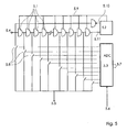
- a solution for clock shift in the picosecond range shows Fig. 5 ,
- a clock 5.4 which can be removed from the clock generator 1.1 quartz exactly, is sent through a certain number of gates 5.1 in an IC. Each of the swept gates delays the clock by a short time, eg 10 picoseconds.
- any tap between the gates can be selected.
- An analog / digital converter 5.3 gets the control voltage from the comparator 1.16. This selects depending on the control voltage a corresponding switch. At output 5.7, the binary value for the set delay can then be tapped, for example.
- the delay time of a gate depends on temperature and supply voltage.
- the clock 5.11 is compared after passing through all gates in a phase comparator 5.2 with the input clock 5.4. With a corresponding number of gates then the clock, which went through all the gates and the input clock 5.4 again have the same phase.
- phase comparator 5.2 a phase difference is detected and output as control voltage gate delay time 5.9. This controls the delay time of the gates.
- the supply voltage of the gates is influenced to control the signal delay. It is also possible to invert one of the two input signals of the phase comparator 5.2 (5.10), in which case only half of the gates are needed. This clarifies Fig.
- the gate transit time can be summarized in blocks of eg 10 or 1 nanosecond and 100 or 10 or 1 picoseconds. Also, with a corresponding division of the gates a direct binary control can be achieved.
Landscapes
- Engineering & Computer Science (AREA)
- Physics & Mathematics (AREA)
- Computer Networks & Wireless Communication (AREA)
- General Physics & Mathematics (AREA)
- Radar, Positioning & Navigation (AREA)
- Remote Sensing (AREA)
- Electromagnetism (AREA)
- Optical Radar Systems And Details Thereof (AREA)
- Measurement Of Optical Distance (AREA)
Applications Claiming Priority (2)
| Application Number | Priority Date | Filing Date | Title |
|---|---|---|---|
| DE102007005187A DE102007005187B4 (de) | 2007-01-29 | 2007-01-29 | Verfahren und Vorrichtung zur Bestimmung einer Entfernung zu einem rückstrahlenden Objekt |
| PCT/EP2008/000615 WO2008092611A1 (de) | 2007-01-29 | 2008-01-28 | Verfahren und vorrichtung zur bestimmung einer entfernung zu einem rückstrahlenden objekt |
Publications (2)
| Publication Number | Publication Date |
|---|---|
| EP2118680A1 EP2118680A1 (de) | 2009-11-18 |
| EP2118680B1 true EP2118680B1 (de) | 2015-11-18 |
Family
ID=39433844
Family Applications (1)
| Application Number | Title | Priority Date | Filing Date |
|---|---|---|---|
| EP08707321.9A Not-in-force EP2118680B1 (de) | 2007-01-29 | 2008-01-28 | Verfahren und vorrichtung zur bestimmung einer entfernung zu einem rückstrahlenden objekt |
Country Status (5)
| Country | Link |
|---|---|
| US (1) | US8405821B2 (enExample) |
| EP (1) | EP2118680B1 (enExample) |
| JP (1) | JP5688900B2 (enExample) |
| DE (1) | DE102007005187B4 (enExample) |
| WO (1) | WO2008092611A1 (enExample) |
Families Citing this family (31)
| Publication number | Priority date | Publication date | Assignee | Title |
|---|---|---|---|---|
| DE102009058817A1 (de) | 2009-12-18 | 2010-08-05 | Daimler Ag | Anlage und Verfahren zum maßhaltigen Rollfalzen eines Bauteils |
| US20120200422A1 (en) * | 2011-02-09 | 2012-08-09 | Baker Hughes Incorporated | Use of Digital Transport Delay to Improve Measurement Fidelity in Swept-Wavelength Systems |
| EP2602635B1 (de) | 2011-12-06 | 2014-02-19 | ELMOS Semiconductor AG | Verfahren zur Vermessung einer Übertragungsstrecke mittels kompensierender Amplitudenmessung und Delta-Sigma-Methode sowie Vorrichtung zur Durchführung des Verfahrens |
| EP2631674A1 (de) | 2012-02-23 | 2013-08-28 | ELMOS Semiconductor AG | Verfahren und Sensorsystem zur Vermessung der Eigenschaften einer Übertragungsstrecke eines Messsystems zwischen Sender und Empfänger |
| EP2653885A1 (de) | 2012-04-18 | 2013-10-23 | ELMOS Semiconductor AG | Sensorsystem und Verfahren zur Vermessung der Übertragungseigenschaften einer Übertragungsstrecke eines Messsystems zwischen einem Sender und einem Empfänger |
| CN103411630A (zh) * | 2012-11-28 | 2013-11-27 | 上海兰宝传感科技股份有限公司 | 智能型偏振反射式光电传感器 |
| DE102013002676B4 (de) | 2013-02-12 | 2023-06-29 | Elmos Semiconductor Se | Kompensiertes Sensorsystem mit einem in der Sensitivität regelbaren Empfänger als kompensierendes Element |
| WO2014131385A1 (de) | 2013-02-27 | 2014-09-04 | Elmos Semiconductor Ag | Multifunktionales optisches mikro-sensor-system |
| DE102014002486B4 (de) | 2013-02-27 | 2017-10-19 | Elmos Semiconductor Aktiengesellschaft | Kompensierendes optisches Sensorsystem |
| CN105143914B (zh) * | 2013-04-17 | 2017-09-01 | 梅查理斯系统股份有限公司 | 用于在近程区域和远程区域中光学间距测量的方法 |
| DE102014002194B4 (de) | 2014-02-12 | 2017-10-19 | Elmos Semiconductor Aktiengesellschaft | Kompensierendes optisches Mikrosystem |
| US9606228B1 (en) | 2014-02-20 | 2017-03-28 | Banner Engineering Corporation | High-precision digital time-of-flight measurement with coarse delay elements |
| CN111181654B (zh) | 2014-03-20 | 2023-02-28 | 艾里尔大学研究与开发有限公司 | 用于控制信号相位的方法、系统及其应用设备 |
| EP2924460A1 (de) | 2014-03-25 | 2015-09-30 | ELMOS Semiconductor AG | Sensorsystem zur Erkennung mindestens eines Objekts in einer Übertragungsstrecke mittels einer Diode |
| EP2924459A1 (de) | 2014-03-25 | 2015-09-30 | ELMOS Semiconductor AG | Sensorsystem zur Erkennung mindestens eines Objekts in einer Übertragungsstrecke |
| EP2924466B1 (de) | 2014-03-25 | 2020-06-03 | Elmos Semiconductor Aktiengesellschaft | Sensorsystem zur Erkennung mindestens eines Objekts in einer Übertragungsstrecke |
| DE102015002283B4 (de) | 2014-05-09 | 2023-01-19 | Elmos Semiconductor Se | Vorrichtung zum insbesondere dreidimensionalen optischen Scannen und Vermessen von Objekten und zur Objekterkennung mittels Lichtlaufzeitmessung und objektabhängiger Ortsauflösung mehrerer verschiedener Einzelscanner |
| DE102014019773B4 (de) | 2014-12-17 | 2023-12-07 | Elmos Semiconductor Se | Vorrichtung und Verfahren zur Unterscheidung von festen Objekten, Kochdunst und Rauch mittels des Displays eines Mobiltelefons |
| DE102014019172B4 (de) | 2014-12-17 | 2023-12-07 | Elmos Semiconductor Se | Vorrichtung und Verfahren zur Unterscheidung von festen Objekten, Kochdunst und Rauch mit einem kompensierenden optischen Messsystem |
| DE102015006174B3 (de) * | 2015-05-08 | 2016-08-11 | Elmos Semiconductor Aktiengesellschaft | Vorrichtung und Verfahren zur Vermessung einer optischen, kapazitiven, induktiven Übertragungsstrecke |
| US10257014B2 (en) | 2015-10-08 | 2019-04-09 | Ariel-University Research And Development Company Ltd. | Method and system for controlling phase of a signal |
| DE102015015248A1 (de) | 2015-11-18 | 2017-05-18 | Elmos Semiconductor Aktiengesellschaft | Einfache Gestenerkennungsvorrichtung |
| DE102015015244A1 (de) | 2015-11-18 | 2017-05-18 | Elmos Semiconductor Aktiengesellschaft | Einfache Gestenerkennungsvorrichtung |
| DE102015015390A1 (de) | 2015-11-18 | 2017-05-18 | Elmos Semiconductor Ag | Einfache Gestenerkennungsvorrichtung |
| DE102015015246A1 (de) | 2015-11-18 | 2017-05-18 | Elmos Semiconductor Aktiengesellschaft | Einfache Gestenerkennungsvorrichtung |
| DE102015015245A1 (de) | 2015-11-18 | 2017-05-18 | Elmos Semiconductor Aktiengesellschaft | Einfache Gestenerkennungsvorrichtung |
| DE102015015389A1 (de) | 2015-11-18 | 2017-05-18 | Elmos Semiconductor Ag | Einfache Gestenerkennungsvorrichtung |
| DE102017100308B3 (de) | 2016-12-06 | 2018-05-30 | Elmos Semiconductor Aktiengesellschaft | Vorrichtung und Verfahren zur Vermessung einer optischen, kapazitiven, induktiven Übertragungsstrecke mit verringerter EMV Empfindlichkeit |
| DE102017200803A1 (de) * | 2017-01-19 | 2018-07-19 | Robert Bosch Gmbh | Überwachungsvorrichtung eines Lidarsystems |
| US11092678B2 (en) | 2018-06-21 | 2021-08-17 | Analog Devices, Inc. | Measuring and removing the corruption of time-of-flight depth images due to internal scattering |
| DE102024117908B3 (de) * | 2024-06-25 | 2025-10-02 | Elmos Semiconductor Se | Sensorsystem zum Bestimmen der Übertragungseigenschaften einer Übertragungsstrecke zwischen Sender und Empfänger in Form von Kopplungsfaktoren |
Family Cites Families (22)
| Publication number | Priority date | Publication date | Assignee | Title |
|---|---|---|---|---|
| US4523093A (en) * | 1981-09-03 | 1985-06-11 | Excellon Industries | Scanning beam reference and read system |
| DE3316630C2 (de) * | 1983-05-06 | 1985-07-25 | Erwin Sick Gmbh Optik-Elektronik, 7808 Waldkirch | Vorrichtung zur Laufzeitbestimmung von Ultraschallimpulsen in einem Fluid |
| US4788441A (en) * | 1985-12-16 | 1988-11-29 | Acme-Cleveland Corporation | Range finder wherein distance between target and source is determined by measuring scan time across a retroreflective target |
| US6122602A (en) * | 1997-05-02 | 2000-09-19 | Endress + Hauser Gmbh + Co. | Method and arrangement for electromagnetic wave distance measurement by the pulse transit time method |
| JPH1123709A (ja) * | 1997-07-07 | 1999-01-29 | Nikon Corp | 距離測定装置 |
| US6043874A (en) * | 1998-04-10 | 2000-03-28 | Spectra Precision, Inc. | System and method for calibrating a laser transmitter |
| DE19830684C1 (de) * | 1998-07-09 | 2000-03-30 | Leuze Electronic Gmbh & Co | Optoelektronische Vorrichtung |
| US6055490A (en) * | 1998-07-27 | 2000-04-25 | Laser Technology, Inc. | Apparatus and method for determining precision reflectivity of highway signs and other reflective objects utilizing an optical range finder instrument |
| JP3849324B2 (ja) * | 1998-11-02 | 2006-11-22 | 株式会社デンソー | 距離測定装置 |
| US7782256B2 (en) * | 1999-03-05 | 2010-08-24 | Era Systems Corporation | Enhanced passive coherent location techniques to track and identify UAVs, UCAVs, MAVs, and other objects |
| DE10022054B4 (de) | 2000-05-06 | 2006-05-24 | Leuze Electronic Gmbh & Co Kg | Optischer Distanzsensor |
| US6711280B2 (en) * | 2001-05-25 | 2004-03-23 | Oscar M. Stafsudd | Method and apparatus for intelligent ranging via image subtraction |
| EP1576385A2 (en) * | 2002-11-26 | 2005-09-21 | James F. Munro | An apparatus for high accuracy distance and velocity measurement and methods thereof |
| DE10300223B3 (de) * | 2003-01-03 | 2004-06-24 | Gerd Reime | Optoelektronische Messanordnung mit Fremdlichtkompensation sowie Verfahren zur phasenkorrekten Kompensation eines Signals der Messanordnung |
| EP1599939A2 (en) * | 2003-02-21 | 2005-11-30 | Inesa Inc. | An apparatus and method for distance measurement with controlled modulation of emitted pulses |
| WO2005054902A1 (de) * | 2003-12-03 | 2005-06-16 | Me-In Gmbh | Schaltungsanordnung zur auswertung eines reflektierten signals |
| EP1815267B1 (de) * | 2004-11-15 | 2015-06-10 | Nanotron Technologies GmbH | Symmetrisches mehrwegverfahren zur bestimmung des abstandes zweier senderempfänger |
| US7375593B2 (en) * | 2005-01-19 | 2008-05-20 | Paul William Ronald Self | Circuits and methods of generating and controlling signals on an integrated circuit |
| DE102005045993B4 (de) * | 2005-07-29 | 2008-11-13 | Gerd Reime | Verfahren zur Lichtlaufzeitmessung |
| WO2007012502A1 (de) * | 2005-07-29 | 2007-02-01 | Gerd Reime | Verfahren und vorrichtung zur entfernungsmessung mittels kapazitiven oder induktiven sensoren |
| US7513160B2 (en) * | 2006-06-05 | 2009-04-07 | Luna Innovations Incorporated | Digital pulsed phase locked loop |
| US7640122B2 (en) * | 2007-11-07 | 2009-12-29 | Institut National D'optique | Digital signal processing in optical systems used for ranging applications |
-
2007
- 2007-01-29 DE DE102007005187A patent/DE102007005187B4/de not_active Expired - Fee Related
-
2008
- 2008-01-28 US US12/524,904 patent/US8405821B2/en not_active Expired - Fee Related
- 2008-01-28 WO PCT/EP2008/000615 patent/WO2008092611A1/de not_active Ceased
- 2008-01-28 JP JP2009546698A patent/JP5688900B2/ja not_active Expired - Fee Related
- 2008-01-28 EP EP08707321.9A patent/EP2118680B1/de not_active Not-in-force
Also Published As
| Publication number | Publication date |
|---|---|
| EP2118680A1 (de) | 2009-11-18 |
| JP5688900B2 (ja) | 2015-03-25 |
| US8405821B2 (en) | 2013-03-26 |
| JP2011511261A (ja) | 2011-04-07 |
| WO2008092611A8 (de) | 2009-09-24 |
| US20100182588A1 (en) | 2010-07-22 |
| DE102007005187B4 (de) | 2008-11-20 |
| DE102007005187A1 (de) | 2008-09-04 |
| WO2008092611A1 (de) | 2008-08-07 |
Similar Documents
| Publication | Publication Date | Title |
|---|---|---|
| EP2118680B1 (de) | Verfahren und vorrichtung zur bestimmung einer entfernung zu einem rückstrahlenden objekt | |
| EP1913420B1 (de) | Verfahren zur lichtlaufzeitmessung | |
| EP3098626B1 (de) | Zeitmessschaltung und optoelektronischer distanzmesser mit einer ebensolchen zeitmessschaltung | |
| EP2315045B1 (de) | Messung von Entfernungen oder Entfernungsänderungen | |
| DE102014100696B3 (de) | Entfernungsmessender Sensor und Verfahren zur Erfassung und Abstandsbestimmung von Objekten | |
| EP2189814B1 (de) | Optoelektronischer Sensor und Verfahren zur Messung von Entfernungen nach dem Lichtlaufzeitprinzip | |
| EP2189805B1 (de) | Optoelektronischer Sensor und Verfahren zur Messung von Entfernungen nach dem Lichtlaufzeitprinzip | |
| EP2773976B1 (de) | Entfernungsmesser | |
| EP2041604B1 (de) | Optisches distanzmessverfahren und entsprechender optischer distanzmesser | |
| EP1876469B1 (de) | Verfahren und Vorrichtung zur optoelektronischen berührungslosen Distanzmessung nach dem Laufzeitprinzip | |
| DE102011056963C5 (de) | Messung von Entfernungen nach dem Signallaufzeitprinzip | |
| EP1910773B1 (de) | Verfahren und vorrichtung zur entfernungsmessung mittels kapazitiven oder induktiven sensoren | |
| EP3339901B1 (de) | Laserdistanzmessmodul mit adc-fehlerkompensation durch variation der samplingzeitpunkte | |
| EP2597482A1 (de) | Vorrichtung und Sensor zur Abstandsmessung mittels der Laufzeit von kompensierten Impulsen | |
| EP1990657B1 (de) | Optischer Entfernungsmesser | |
| EP2088453A1 (de) | Optoelektronischer Sensor zur Entfernungsmessung | |
| DE102007013714A1 (de) | Optoelektronischer Sensor und Verfahren zur Messung einer Entfernung oder einer Entfernungsänderung | |
| EP2189804A1 (de) | Optoelektronischer Sensor und Verfahren zur Messung von Entfernungen nach dem Lichtlaufzeitprinzip | |
| EP2558883A1 (de) | Entfernungsmessgerät mit homogenisierender messauswertung | |
| DE3419117A1 (de) | Optoelektrisches entfernungsmessgeraet mit einem zeitdiskriminator zur genauen ermittlung der zeitfolge elektrischer impulse | |
| DE10018948B4 (de) | Optoelektronische Vorrichtung | |
| DE102010013751A1 (de) | Vorrichtung zur Laufzeitmessung mit Pulsformung zur Entfernungsbestimmung | |
| DE10236486B4 (de) | Vorrichtung zur berührungslosen Entfernungsmessung | |
| EP1876468B1 (de) | Vorrichtung und Verfahren zur optoelektronischen berührungslosen Distanzmessung | |
| DE102015121578B3 (de) | Sendevorrichtung und Verfahren zum Erzeugen eines Sendesignals |
Legal Events
| Date | Code | Title | Description |
|---|---|---|---|
| PUAI | Public reference made under article 153(3) epc to a published international application that has entered the european phase |
Free format text: ORIGINAL CODE: 0009012 |
|
| 17P | Request for examination filed |
Effective date: 20090824 |
|
| AK | Designated contracting states |
Kind code of ref document: A1 Designated state(s): AT BE BG CH CY CZ DE DK EE ES FI FR GB GR HR HU IE IS IT LI LT LU LV MC MT NL NO PL PT RO SE SI SK TR |
|
| DAX | Request for extension of the european patent (deleted) | ||
| GRAP | Despatch of communication of intention to grant a patent |
Free format text: ORIGINAL CODE: EPIDOSNIGR1 |
|
| RIC1 | Information provided on ipc code assigned before grant |
Ipc: G01S 17/10 20060101ALI20150521BHEP Ipc: G01S 7/497 20060101ALI20150521BHEP Ipc: G01S 7/486 20060101ALI20150521BHEP Ipc: G01S 7/487 20060101AFI20150521BHEP |
|
| INTG | Intention to grant announced |
Effective date: 20150608 |
|
| GRAS | Grant fee paid |
Free format text: ORIGINAL CODE: EPIDOSNIGR3 |
|
| GRAA | (expected) grant |
Free format text: ORIGINAL CODE: 0009210 |
|
| AK | Designated contracting states |
Kind code of ref document: B1 Designated state(s): AT BE BG CH CY CZ DE DK EE ES FI FR GB GR HR HU IE IS IT LI LT LU LV MC MT NL NO PL PT RO SE SI SK TR |
|
| REG | Reference to a national code |
Ref country code: GB Ref legal event code: FG4D Free format text: NOT ENGLISH |
|
| REG | Reference to a national code |
Ref country code: CH Ref legal event code: EP |
|
| REG | Reference to a national code |
Ref country code: AT Ref legal event code: REF Ref document number: 761828 Country of ref document: AT Kind code of ref document: T Effective date: 20151215 |
|
| REG | Reference to a national code |
Ref country code: IE Ref legal event code: FG4D Free format text: LANGUAGE OF EP DOCUMENT: GERMAN |
|
| REG | Reference to a national code |
Ref country code: DE Ref legal event code: R096 Ref document number: 502008013595 Country of ref document: DE |
|
| REG | Reference to a national code |
Ref country code: FR Ref legal event code: PLFP Year of fee payment: 9 |
|
| REG | Reference to a national code |
Ref country code: NL Ref legal event code: MP Effective date: 20160218 |
|
| REG | Reference to a national code |
Ref country code: LT Ref legal event code: MG4D |
|
| PG25 | Lapsed in a contracting state [announced via postgrant information from national office to epo] |
Ref country code: IT Free format text: LAPSE BECAUSE OF FAILURE TO SUBMIT A TRANSLATION OF THE DESCRIPTION OR TO PAY THE FEE WITHIN THE PRESCRIBED TIME-LIMIT Effective date: 20151118 Ref country code: IS Free format text: LAPSE BECAUSE OF FAILURE TO SUBMIT A TRANSLATION OF THE DESCRIPTION OR TO PAY THE FEE WITHIN THE PRESCRIBED TIME-LIMIT Effective date: 20160318 Ref country code: NL Free format text: LAPSE BECAUSE OF FAILURE TO SUBMIT A TRANSLATION OF THE DESCRIPTION OR TO PAY THE FEE WITHIN THE PRESCRIBED TIME-LIMIT Effective date: 20151118 Ref country code: ES Free format text: LAPSE BECAUSE OF FAILURE TO SUBMIT A TRANSLATION OF THE DESCRIPTION OR TO PAY THE FEE WITHIN THE PRESCRIBED TIME-LIMIT Effective date: 20151118 Ref country code: NO Free format text: LAPSE BECAUSE OF FAILURE TO SUBMIT A TRANSLATION OF THE DESCRIPTION OR TO PAY THE FEE WITHIN THE PRESCRIBED TIME-LIMIT Effective date: 20160218 Ref country code: HR Free format text: LAPSE BECAUSE OF FAILURE TO SUBMIT A TRANSLATION OF THE DESCRIPTION OR TO PAY THE FEE WITHIN THE PRESCRIBED TIME-LIMIT Effective date: 20151118 Ref country code: LT Free format text: LAPSE BECAUSE OF FAILURE TO SUBMIT A TRANSLATION OF THE DESCRIPTION OR TO PAY THE FEE WITHIN THE PRESCRIBED TIME-LIMIT Effective date: 20151118 |
|
| PG25 | Lapsed in a contracting state [announced via postgrant information from national office to epo] |
Ref country code: PT Free format text: LAPSE BECAUSE OF FAILURE TO SUBMIT A TRANSLATION OF THE DESCRIPTION OR TO PAY THE FEE WITHIN THE PRESCRIBED TIME-LIMIT Effective date: 20160318 Ref country code: SE Free format text: LAPSE BECAUSE OF FAILURE TO SUBMIT A TRANSLATION OF THE DESCRIPTION OR TO PAY THE FEE WITHIN THE PRESCRIBED TIME-LIMIT Effective date: 20151118 Ref country code: FI Free format text: LAPSE BECAUSE OF FAILURE TO SUBMIT A TRANSLATION OF THE DESCRIPTION OR TO PAY THE FEE WITHIN THE PRESCRIBED TIME-LIMIT Effective date: 20151118 Ref country code: LV Free format text: LAPSE BECAUSE OF FAILURE TO SUBMIT A TRANSLATION OF THE DESCRIPTION OR TO PAY THE FEE WITHIN THE PRESCRIBED TIME-LIMIT Effective date: 20151118 Ref country code: PL Free format text: LAPSE BECAUSE OF FAILURE TO SUBMIT A TRANSLATION OF THE DESCRIPTION OR TO PAY THE FEE WITHIN THE PRESCRIBED TIME-LIMIT Effective date: 20151118 Ref country code: BE Free format text: LAPSE BECAUSE OF NON-PAYMENT OF DUE FEES Effective date: 20160131 Ref country code: GR Free format text: LAPSE BECAUSE OF FAILURE TO SUBMIT A TRANSLATION OF THE DESCRIPTION OR TO PAY THE FEE WITHIN THE PRESCRIBED TIME-LIMIT Effective date: 20160219 |
|
| PG25 | Lapsed in a contracting state [announced via postgrant information from national office to epo] |
Ref country code: CZ Free format text: LAPSE BECAUSE OF FAILURE TO SUBMIT A TRANSLATION OF THE DESCRIPTION OR TO PAY THE FEE WITHIN THE PRESCRIBED TIME-LIMIT Effective date: 20151118 |
|
| REG | Reference to a national code |
Ref country code: DE Ref legal event code: R097 Ref document number: 502008013595 Country of ref document: DE |
|
| PG25 | Lapsed in a contracting state [announced via postgrant information from national office to epo] |
Ref country code: LU Free format text: LAPSE BECAUSE OF FAILURE TO SUBMIT A TRANSLATION OF THE DESCRIPTION OR TO PAY THE FEE WITHIN THE PRESCRIBED TIME-LIMIT Effective date: 20160128 Ref country code: RO Free format text: LAPSE BECAUSE OF FAILURE TO SUBMIT A TRANSLATION OF THE DESCRIPTION OR TO PAY THE FEE WITHIN THE PRESCRIBED TIME-LIMIT Effective date: 20151118 Ref country code: SK Free format text: LAPSE BECAUSE OF FAILURE TO SUBMIT A TRANSLATION OF THE DESCRIPTION OR TO PAY THE FEE WITHIN THE PRESCRIBED TIME-LIMIT Effective date: 20151118 Ref country code: DK Free format text: LAPSE BECAUSE OF FAILURE TO SUBMIT A TRANSLATION OF THE DESCRIPTION OR TO PAY THE FEE WITHIN THE PRESCRIBED TIME-LIMIT Effective date: 20151118 Ref country code: EE Free format text: LAPSE BECAUSE OF FAILURE TO SUBMIT A TRANSLATION OF THE DESCRIPTION OR TO PAY THE FEE WITHIN THE PRESCRIBED TIME-LIMIT Effective date: 20151118 |
|
| REG | Reference to a national code |
Ref country code: CH Ref legal event code: PL |
|
| PLBE | No opposition filed within time limit |
Free format text: ORIGINAL CODE: 0009261 |
|
| STAA | Information on the status of an ep patent application or granted ep patent |
Free format text: STATUS: NO OPPOSITION FILED WITHIN TIME LIMIT |
|
| PG25 | Lapsed in a contracting state [announced via postgrant information from national office to epo] |
Ref country code: MC Free format text: LAPSE BECAUSE OF FAILURE TO SUBMIT A TRANSLATION OF THE DESCRIPTION OR TO PAY THE FEE WITHIN THE PRESCRIBED TIME-LIMIT Effective date: 20151118 |
|
| 26N | No opposition filed |
Effective date: 20160819 |
|
| PG25 | Lapsed in a contracting state [announced via postgrant information from national office to epo] |
Ref country code: CH Free format text: LAPSE BECAUSE OF NON-PAYMENT OF DUE FEES Effective date: 20160131 Ref country code: LI Free format text: LAPSE BECAUSE OF NON-PAYMENT OF DUE FEES Effective date: 20160131 |
|
| REG | Reference to a national code |
Ref country code: IE Ref legal event code: MM4A |
|
| PG25 | Lapsed in a contracting state [announced via postgrant information from national office to epo] |
Ref country code: SI Free format text: LAPSE BECAUSE OF FAILURE TO SUBMIT A TRANSLATION OF THE DESCRIPTION OR TO PAY THE FEE WITHIN THE PRESCRIBED TIME-LIMIT Effective date: 20151118 |
|
| REG | Reference to a national code |
Ref country code: FR Ref legal event code: PLFP Year of fee payment: 10 |
|
| PG25 | Lapsed in a contracting state [announced via postgrant information from national office to epo] |
Ref country code: IE Free format text: LAPSE BECAUSE OF NON-PAYMENT OF DUE FEES Effective date: 20160128 |
|
| REG | Reference to a national code |
Ref country code: AT Ref legal event code: MM01 Ref document number: 761828 Country of ref document: AT Kind code of ref document: T Effective date: 20160128 |
|
| PG25 | Lapsed in a contracting state [announced via postgrant information from national office to epo] |
Ref country code: AT Free format text: LAPSE BECAUSE OF NON-PAYMENT OF DUE FEES Effective date: 20160128 |
|
| PG25 | Lapsed in a contracting state [announced via postgrant information from national office to epo] |
Ref country code: MT Free format text: LAPSE BECAUSE OF FAILURE TO SUBMIT A TRANSLATION OF THE DESCRIPTION OR TO PAY THE FEE WITHIN THE PRESCRIBED TIME-LIMIT Effective date: 20151118 |
|
| REG | Reference to a national code |
Ref country code: FR Ref legal event code: PLFP Year of fee payment: 11 |
|
| PGFP | Annual fee paid to national office [announced via postgrant information from national office to epo] |
Ref country code: GB Payment date: 20180125 Year of fee payment: 11 Ref country code: DE Payment date: 20171215 Year of fee payment: 11 |
|
| PG25 | Lapsed in a contracting state [announced via postgrant information from national office to epo] |
Ref country code: CY Free format text: LAPSE BECAUSE OF FAILURE TO SUBMIT A TRANSLATION OF THE DESCRIPTION OR TO PAY THE FEE WITHIN THE PRESCRIBED TIME-LIMIT Effective date: 20151118 Ref country code: HU Free format text: LAPSE BECAUSE OF FAILURE TO SUBMIT A TRANSLATION OF THE DESCRIPTION OR TO PAY THE FEE WITHIN THE PRESCRIBED TIME-LIMIT; INVALID AB INITIO Effective date: 20080128 |
|
| PGFP | Annual fee paid to national office [announced via postgrant information from national office to epo] |
Ref country code: FR Payment date: 20180124 Year of fee payment: 11 |
|
| PG25 | Lapsed in a contracting state [announced via postgrant information from national office to epo] |
Ref country code: TR Free format text: LAPSE BECAUSE OF FAILURE TO SUBMIT A TRANSLATION OF THE DESCRIPTION OR TO PAY THE FEE WITHIN THE PRESCRIBED TIME-LIMIT Effective date: 20151118 |
|
| PG25 | Lapsed in a contracting state [announced via postgrant information from national office to epo] |
Ref country code: BG Free format text: LAPSE BECAUSE OF FAILURE TO SUBMIT A TRANSLATION OF THE DESCRIPTION OR TO PAY THE FEE WITHIN THE PRESCRIBED TIME-LIMIT Effective date: 20151118 |
|
| REG | Reference to a national code |
Ref country code: DE Ref legal event code: R119 Ref document number: 502008013595 Country of ref document: DE |
|
| GBPC | Gb: european patent ceased through non-payment of renewal fee |
Effective date: 20190128 |
|
| PG25 | Lapsed in a contracting state [announced via postgrant information from national office to epo] |
Ref country code: DE Free format text: LAPSE BECAUSE OF NON-PAYMENT OF DUE FEES Effective date: 20190801 Ref country code: FR Free format text: LAPSE BECAUSE OF NON-PAYMENT OF DUE FEES Effective date: 20190131 |
|
| PG25 | Lapsed in a contracting state [announced via postgrant information from national office to epo] |
Ref country code: GB Free format text: LAPSE BECAUSE OF NON-PAYMENT OF DUE FEES Effective date: 20190128 |