EP2118680B1 - Method and device for determining the distance to a retroreflective object - Google Patents
Method and device for determining the distance to a retroreflective object Download PDFInfo
- Publication number
- EP2118680B1 EP2118680B1 EP08707321.9A EP08707321A EP2118680B1 EP 2118680 B1 EP2118680 B1 EP 2118680B1 EP 08707321 A EP08707321 A EP 08707321A EP 2118680 B1 EP2118680 B1 EP 2118680B1
- Authority
- EP
- European Patent Office
- Prior art keywords
- signal
- electrical
- reference signal
- comparator
- amplitude
- Prior art date
- Legal status (The legal status is an assumption and is not a legal conclusion. Google has not performed a legal analysis and makes no representation as to the accuracy of the status listed.)
- Not-in-force
Links
Images


Classifications
-
- G—PHYSICS
- G01—MEASURING; TESTING
- G01S—RADIO DIRECTION-FINDING; RADIO NAVIGATION; DETERMINING DISTANCE OR VELOCITY BY USE OF RADIO WAVES; LOCATING OR PRESENCE-DETECTING BY USE OF THE REFLECTION OR RERADIATION OF RADIO WAVES; ANALOGOUS ARRANGEMENTS USING OTHER WAVES
- G01S7/00—Details of systems according to groups G01S13/00, G01S15/00, G01S17/00
- G01S7/48—Details of systems according to groups G01S13/00, G01S15/00, G01S17/00 of systems according to group G01S17/00
- G01S7/483—Details of pulse systems
- G01S7/486—Receivers
- G01S7/487—Extracting wanted echo signals, e.g. pulse detection
-
- G—PHYSICS
- G01—MEASURING; TESTING
- G01S—RADIO DIRECTION-FINDING; RADIO NAVIGATION; DETERMINING DISTANCE OR VELOCITY BY USE OF RADIO WAVES; LOCATING OR PRESENCE-DETECTING BY USE OF THE REFLECTION OR RERADIATION OF RADIO WAVES; ANALOGOUS ARRANGEMENTS USING OTHER WAVES
- G01S17/00—Systems using the reflection or reradiation of electromagnetic waves other than radio waves, e.g. lidar systems
- G01S17/02—Systems using the reflection of electromagnetic waves other than radio waves
- G01S17/06—Systems determining position data of a target
- G01S17/08—Systems determining position data of a target for measuring distance only
- G01S17/10—Systems determining position data of a target for measuring distance only using transmission of interrupted, pulse-modulated waves
-
- G—PHYSICS
- G01—MEASURING; TESTING
- G01S—RADIO DIRECTION-FINDING; RADIO NAVIGATION; DETERMINING DISTANCE OR VELOCITY BY USE OF RADIO WAVES; LOCATING OR PRESENCE-DETECTING BY USE OF THE REFLECTION OR RERADIATION OF RADIO WAVES; ANALOGOUS ARRANGEMENTS USING OTHER WAVES
- G01S7/00—Details of systems according to groups G01S13/00, G01S15/00, G01S17/00
- G01S7/48—Details of systems according to groups G01S13/00, G01S15/00, G01S17/00 of systems according to group G01S17/00
- G01S7/483—Details of pulse systems
- G01S7/486—Receivers
- G01S7/4865—Time delay measurement, e.g. time-of-flight measurement, time of arrival measurement or determining the exact position of a peak
-
- G—PHYSICS
- G01—MEASURING; TESTING
- G01S—RADIO DIRECTION-FINDING; RADIO NAVIGATION; DETERMINING DISTANCE OR VELOCITY BY USE OF RADIO WAVES; LOCATING OR PRESENCE-DETECTING BY USE OF THE REFLECTION OR RERADIATION OF RADIO WAVES; ANALOGOUS ARRANGEMENTS USING OTHER WAVES
- G01S7/00—Details of systems according to groups G01S13/00, G01S15/00, G01S17/00
- G01S7/48—Details of systems according to groups G01S13/00, G01S15/00, G01S17/00 of systems according to group G01S17/00
- G01S7/497—Means for monitoring or calibrating
Definitions
- the invention relates to a method and a device for determining a distance to a retroreflective object and possibly the reflectance of the object according to the preamble of claims 1 and 9.
- a door opens when a measuring arrangement detects the approach of an object. Or a revolving door stops as soon as an obstacle is detected. Changes may occur due to the approach, presence or removal of an object and are detected by the measuring device.
- One way of distance measurement is to use the light transit time.
- a laser beam is directed at the object to be measured and the reflected light is measured.
- the delay until the reflected light arrives at the receiver is a value for the distance the light has traveled.
- the speed of light is around 300,000 km / s.
- a light pulse that covers a distance of 3 m takes about 10 nanoseconds.
- fast lasers or fast photodiodes and amplifiers are necessary.
- One solution uses the possibility of transforming the runtime information into an easier-to-handle frequency range (cf. DE 100 22 054 A1 ). This is for the purpose of determination the duration of the emitted light with a high frequency, z. B. modulated several hundred MHz.
- the received light is then mixed with a second frequency that is only slightly different than the transmitted frequency.
- a third, significantly lower frequency is formed, which can be processed in the wider circuit easier than the original high modulation frequency.
- this third frequency is in the phase, the information of the light transit time. Since the third frequency is usually downsampled in a frequency range of a few kHz, the determination of the phase information and thus the light transit time is very simple.
- the determined difference value is used to drive a phase shifter designed as a digital delay element, and the delay time is changed until the difference value becomes small.
- the disadvantage of this system is that only a certain distance range is covered, moreover, the phase information repeats periodically, so that indeterminacy occurs. In order to avoid these vagaries, extensive measures such as modulation with different frequencies are necessary. This system basically works with more than one light pulse, otherwise no mixing process can take place. In known systems, at least several thousand individual pulses are emitted to obtain several periods of the signal downconverted to the third frequency.
- a second method of determining the light transit time is the direct measurement of a single pulse.
- uncertainties are excluded, as they are disadvantageous in the method described above.
- the advantage of a single pulse is the possible higher power.
- much higher demands are placed on the detection of such a light pulse in the receiver.
- the receiver To measure distances below 15 cm, the receiver must have a response time under a nanosecond.
- a perfectly emitted light pulse with a rise time of theoretically zero is "softened” by the inherently limited bandwidth in the receiver. In an evaluation e.g. At a threshold value of 50% of the maximum amplitude, this results in a "delay", which is generally dependent on the temperature, but also on the received energy.
- the received signal is usually regulated to a fixed amplitude. This regulation of the amplitude can lead to an undesirable time shift. Also, determining the exact time to receive turns out to be difficult with very small signals and therefore high noise. By the way, should the received pulse with strong reflection the Do not overdrive the photodiode or the preamplifier, as the resulting nonlinearities have a negative effect on the accuracy of the reception time.
- a fast photodiode usually an avalanche photodiode
- a fast preamplifier must also be provided here. Frequency ranges up to the gigahertz range are not uncommon.
- extraneous light which in extreme cases is several thousand times stronger than the reflected light of the emitted pulse. All these influences have a negative effect on the accuracy of the measurement.
- the method works exclusively with continuously successive pulses alternately from two different but electrically identical light sources and is therefore limited in its pulse power due to the temperature limit in the light-emitting diodes used.
- a disadvantage of this method however, a possibly occurring, not exactly ausregelbares to zero signal, created for example by an asymmetry of the light sources used or other electronic components.
- This residual signal can lead to a measurement error in strong ambient light radiation and at the same time strong reflection of the transmission signal.
- the said asymmetry arises, for example, when an LED has a different time Behavior when switching on or off has or when different light sources, such as laser and LED are used mixed.
- the WO 2005/054902 A1 shows an energy-saving circuit arrangement for evaluating a clocked, reflected from an object, optical signal.
- the output signals received by a receiver on the basis of the optical signal reflected from the object are compared with reference signal pulses whose amplitude depends on the output signal of the comparator.
- the reference signal pulses occur simultaneously with the output pulses received by the receiver.
- the present invention has the object to provide a working with single pulses high energy density method.
- This object is achieved by a method and a device for determining a distance to a retroreflective object with the features of claim 1 or 9.
- the invention makes use of the fact that not a reflected pulse is measured and evaluated, but that a possible pulse in the receiver is made to disappear.
- the received pulse is preferably "embedded" between two reference pulses also originating from a light path or electrically transmitted, so that it can no longer be recognized as a single pulse. However, it is sufficient to compare with a reference pulse. Influencing the start time, which causes the light pulse to "disappear", then corresponds to the transit time of the light pulse from the transmitted light source to the reflecting object and back to the receiver and thus represents a value for the distance.
- the pulses can also be detected before and after the actual transmission signal and an average value can be formed from their amplitudes, which corresponds to the proportion of the reference signal and is compared with the amplitude value from the light signal.
- the clock change signals alone may under certain circumstances still contain an error potential in that rise and fall times of the light-emitting diodes are included.
- a clock change signal is used alone and compared to an amplitude value independent of the time of flight, these errors can be reduced, although a possible temperature drift can then have a slightly greater influence.
- the amplitude value adjusted by the amplitude control is used as the reference at the preamplifier. Namely, if a clock change signal is controlled or canceled so that it corresponds to this reference value, this is due to the isochronous occurrence of the clock change signals equalize a balancing of the two clock change signals to the same size. Alternatively or additionally, a residual error can be completely eliminated by a further regulation
- the light emitting diodes possibly occurring asymmetries or tolerances are corrected and have no effect on the measurement accuracy, not even under high external light influence.
- a clock control 1.1 e.g. a correspondingly programmed microcontroller, delivers pulses to at least one transmitted light source 1.8 and a second, located in the immediate vicinity of the receiver second light source 1.9, which serves as a reference light source.
- the light sources may be light emitting diodes or laser diodes or alternatively both types mixed. At least one of the two light sources is adjustable in phase and amplitude by a determinable amount.
- the transmission light source 1.8 sends e.g. every 10 ms a pulse of 100 ns. This traverses the light path 1.24 and 1.25 to the object and from the object 1.26 to a receiver, such as e.g. the photodiode 1.10 and would appear without further action as a single pulse in the amplifier 1.11. To detect the time of arrival, the problems mentioned above would now occur in the prior art.
- a reference pulse 2.1 according to Fig. 2 sent. This is led from the second light source 1.9 directly over a short path in the photodiode 1.10.
- the actual transmit pulse 2.2 ( Fig. 2 ) of the transmission light source 1.8.
- another reference pulse 2.3 emanates from the second light source 1.9.
- the transmission pulse 2.2 is embedded between two reference pulses.
- the method described also works with only one reference pulse.
- the reference pulses can also be transmitted directly as electrical reference signals to the preamplifier 1.10 or the following regulations. However, rapidly changing external light influences can then lead to short-term measured value errors.
- the light of the transmitted light source 1.8 and the light of the reference light source 1.9 initially arrive at the photodiode 1.10 with different intensity.
- the receiver converts the received signal, ie the received transmission signal 2.2 and possibly the at least one received reference signal 2.1, 2.3 into an electrical transmission signal 2.5 or an electrical reference signal 2.4, 2.6.
- the electrical reference signal can also be introduced directly into the circuit and subsequent regulation without the detour via a light path.
- the photodiode amplifier, the preamplifier 1.11 during the duration of all pulses by control line 1.30 is activated.
- the temporal range is considered, in which the light sources are active. Falsifications of the received signal by the increase in light at the first reference pulse 2.1 and light fall at the end of the second reference pulse 2.3 are thereby excluded.
- a decomposition of the received signal according to Fig. 2 in the clock sections A, B, C, D, E shows on the one hand two areas B, D with clock change signals between adjacent pulses 2.1, 2.2 and 2.2, 2.3 and on the other hand, the areas A, C, E, where the clock change signal has subsided and only still pure amplitude information is pending.
- the signal path switch 1.17 switches the range A, E to a first input 1.19a of a comparator 1.19.
- the area C is inverted via inverting stage 1.12 to the areas A + E with signal path switch 1.18 to the same input 1.19a of the comparator 1.19.
- the second input 1.19b of the comparator 1.19 is located at a, formed by two equal resistances 1.13 averaging of the direct and the inverted signal of the preamplifier 1.11. Since both equally large signals cancel each other by alternating voltages, a pure DC voltage component is thus present at the summation point between the two resistors.
- the comparator 1.19 itself can be implemented as a high-gain operational amplifier with integration 1.31 of the input signal.
- This comparator 1.19 is to detect even the smallest difference of the input values and to provide them at the output 1.19c as control value 1.29.
- This control value can be evaluated for the detection of changes to or as a result of the object and thus serves e.g. for detecting the position, position and movement of the object 1.26.
- the circuits 1.31 of the comparators 1.16, 1.19 and 1.22 correspond to an integrating "sample and hold" function.
- the comparator 1.19 e.g. this means that the mean value of the signal sampled with the signal path switch 1.17 or 1.18 is stored until the next clock cycle.
- the amplitude values of the reference pulses 2.1 and 2.3 are compared with the amplitude values of the transmit pulse 2.2.
- a difference between the two values leads to a control voltage 1.29 at the output 1.19c of the comparator 1.19.
- this control voltage at least one of the two light sources 1.8 and 1.9 is readjusted in its amplitude until no difference of the input voltages at the comparator 1.19 is present or at least minimal.
- the reference light source 1.9 is controlled directly via the amplitude control 1.6, while the transmission light source 1.8 is controlled inversely via the amplitude control 1.7 and the inverter 1.12.
- the transmission step is e.g. regulated to high power, while the reference light source 1.9 is adjusted so far until the reference pulses 2.1, 2.3 appear the same as the transmission pulse 2.2 in the receiver 1.10. If we omit the time shift due to the light paths 1.24 and 1.25, the total transmit pulse in the receive signal consisting of the first reference signal 2.1, the transmit signal 2.2 and the second reference signal 2.3 is not visible as such. He has "disappeared", so to speak.
- the transmission pulse is embedded in a second signal environment so that it is no longer visible, but should be determined in the case of a light time measurement, the time that this pulse has traveled on the light paths 1.24 and 1.25.
- the 1.24 light range is 15 cm long, and thus 30 cm back and forth.
- the pulse takes a nanosecond.
- the pulse arrives in the receiver as having a "delay" of one nanosecond.
- This state shows in Fig.2 the representation of the received signal 2.4 of the first reference pulse 2.1, the received signal 2.5 delayed by a nanosecond incoming transmission pulse 2.2 and the received signal 2.6 of the second reference pulse 2.3.
- the delay is exaggerated; in practice, a delay of 1 nanosecond is barely visible in relation to the transmission pulse length. However, a short gap of one nanosecond will arise between the received signal 2.4 of the first reference pulse 2.1 and the received signal 2.5 of the incoming transmit pulse 2.2, in which no light from one of the two light sources 1.8 and 1.9 hits the photodiode 1.10.
- a “slow” photodiode and a “slow” preamp can not resolve this short pulse. Since, in addition, the rise times for commercially available light-emitting diodes and driver stages in C-MOS technology are definitely longer than a nanosecond, in the best case a strongly attenuated pulse whose amplitude would be difficult to determine would appear at the output of preamplifier 1.11.
- the transit time of the light signal is determined by the method described here, one is no longer dependent on an accurate measurement of the received light pulse. Rather, it is even advantageous if the received pulse is "ground” by limiting the photodiode or preamplifier bandwidth.
- the energy of the pulse goes through the grinding, i. when passing through an amplifier with reduced bandwidth, not lost.
- From a pulse of one nanosecond and a pulse height of e.g. 10 mV is then applied e.g. a pulse height of 10 microvolts, but with a length of 1000 nanoseconds.
- This "small” but long pulse can now be easily amplified with C-MOS technology.
- the photodiode amplifier 1.11 can also be designed as a high-gain limiter amplifier. The temporally precise assignment of the received pulse 2.5 is indeed lost, but is not needed in the method described here.
- the signal 2.9 in Fig. 2 shows the amplitude of the received signal at the output of preamplifier 1.11, which has not yet been corrected in time. From the very short pulses at the transition between transmit and reference pulses has now become a long and easy to process pulse. In a further step, the received signal 2.9 is now examined for these pulses. For this purpose, the amplitude differences in the areas B and D are compared with the Signalwegschalter 1.14 and 1.15. The signal path switch 1.14 switches during the area B to a first input 1.16a of a comparator 1.16. The area D is given inverted to the area B with signal path switch 1.15 to the same input 1.16a of the comparator 1.16.
- the second input 1.16b of the comparator 1.16 is located at an averaging formed by two equal resistances 1.13 from the direct and the inverted signal of the preamplifier 1.11. Since both equally large signals cancel each other by alternating voltages, a pure DC voltage component is thus present at the summation point between the two resistors. Only a DC drift of the output voltage of preamplifier 1.11 and inversion stage 1.12 shares the sum point and thus the second input 1.16b of the comparator 1.16. As a result of this measure, the influence of a temperature-induced DC drift of the amplifier 1.11 and of the inverter 1.12 in the comparator 1.16 is canceled out.
- the comparator can be identical to the comparator 1.19, ie as a high-gain operational amplifier with integration of the input signal.
- the execution of the comparators described here can also be different, it is only essential that they compare two signals with each other while having a high gain. A difference between the two input values of comparator 1.16 leads to a control voltage 1.27 at the output of comparator 1.16.
- the information from the sections B and D are compared directly with each other, as in FIG. 1 is shown.
- properties of the LEDs can falsify the result.
- One way to reduce this influence is to cancel or minimize the amplitude of only one clock change signal compared to the amplitude of a reference value pending in the regulated state of the amplitude control at the output 1.11b of the preamplifier 1.19.
- the control voltage 1.27 is given to a control voltage processing 1.2. Depending on the control voltage 1.27, this stage shifts the phases of the reference pulses 2.1, 2.3 and the transmit pulse 2.2 relative to one another with the aid of the analog or digital phase controls 1.3, 1.4, 1.5 so that the pulses applied to the preamplifier 1.11 disappear in the time periods B and D.
- the transmission pulse 2.2 or only the reference pulses 2.1 and / or 2.3 are shifted in time, but of course also transmission and reference pulses can be shifted to each other.
- the reference pulses and the transmission pulse must be shifted by exactly one nanosecond to each other. Then the timing change pulses of the received signal 2.9 are extinguished according to signal 2.10 and at the output 1.11b of the amplifier 1.11 is only the amplifier noise without any isochronous shares.
- the first and the second reference pulse are combined and fed to the amplitude control 1.6.
- control voltage 1.27 is then the information of the light runtime.
- the value of the light runtime can also be obtained as a digital value.
- a determination of the light transit time according to the method described so far has the advantage of very high detection sensitivity with a very high dynamic range of the reflection. If necessary, the method described also works with only one reference pulse. However, rapidly changing extraneous light influences can then lead to short-term measured value errors.
- Fig. 4 shows the advantage of two reference pulses.
- the received signals 2.4, 2.6 of the reference pulses and the received signal 2.5 of the transmitted pulse are also influenced. Since the mean value 4.2 for the first reference pulse, the mean value 4.3 for the transmit pulse, and the mean value 4.4 for the second reference pulse are formed in the integration circuit 1.31, the resulting common mean value of the reference pulses 2.4 and 2.6 is equal to the mean value 4.3 of the transmit pulse. Fast ambient light changes thus have no influence on the measurement.
- the received signal in the periods B and D can not be canceled precisely.
- This difference in the rise and fall times arises, for example, with light emitting diodes of different batches or when using a laser diode as a transmitter and cost reasons of an LED as a reference light source.
- Fig. 3 represents this state in the signals 3.1, 3.2 and 3.3.
- the output signal 3.4 of the preamplifier 1.11 shows an asymmetrical course without time correction of the reference or transmit pulse. After adjustment by means of comparator 1.16, although the desired symmetry results, but a residual error in the clock ranges B and D is present.
- the clock sections A, C and E are compared with the clock sections B and D by means of a further comparator 1.22.
- the signal path switch 1.20 switches the clock sections A, C, E to an input 1.22a of the comparator 1.22, while the signal path switch 1.21 switches the clock sections B, D to the other input 1.22b.
- the output 1.22c of the comparator 1.22 is connected to the control voltage processing 1.2.
- the control voltage processing 1.2 thus acts on the phase control, which is e.g. the transmission pulse is extended or shortened until the residual error 3.5 is completely extinguished and again only the amplifier noise is present without isochronous portions of the photodiode amplifier 1.11. It does not matter whether the transmit pulse or the reference pulses are influenced in the time length or the reference pulses are shifted in their position. All three regulations, ie amplitude, time shift and compensation of the reaction time can be active at the same time, without disturbing each other.
- a digital signal delay can be used for this purpose.
- a desired resolution of eg 1.5 mm then means a step size of 10 picoseconds.
- the clock rate of a possible microprocessor would theoretically be 100 gigahertz, a clock frequency z.Zt. not yet possible.
- a solution for clock shift in the picosecond range shows Fig. 5 ,
- a clock 5.4 which can be removed from the clock generator 1.1 quartz exactly, is sent through a certain number of gates 5.1 in an IC. Each of the swept gates delays the clock by a short time, eg 10 picoseconds.
- any tap between the gates can be selected.
- An analog / digital converter 5.3 gets the control voltage from the comparator 1.16. This selects depending on the control voltage a corresponding switch. At output 5.7, the binary value for the set delay can then be tapped, for example.
- the delay time of a gate depends on temperature and supply voltage.
- the clock 5.11 is compared after passing through all gates in a phase comparator 5.2 with the input clock 5.4. With a corresponding number of gates then the clock, which went through all the gates and the input clock 5.4 again have the same phase.
- phase comparator 5.2 a phase difference is detected and output as control voltage gate delay time 5.9. This controls the delay time of the gates.
- the supply voltage of the gates is influenced to control the signal delay. It is also possible to invert one of the two input signals of the phase comparator 5.2 (5.10), in which case only half of the gates are needed. This clarifies Fig.
- the gate transit time can be summarized in blocks of eg 10 or 1 nanosecond and 100 or 10 or 1 picoseconds. Also, with a corresponding division of the gates a direct binary control can be achieved.
Landscapes
- Engineering & Computer Science (AREA)
- Physics & Mathematics (AREA)
- Computer Networks & Wireless Communication (AREA)
- General Physics & Mathematics (AREA)
- Radar, Positioning & Navigation (AREA)
- Remote Sensing (AREA)
- Electromagnetism (AREA)
- Optical Radar Systems And Details Thereof (AREA)
- Measurement Of Optical Distance (AREA)
Description
Die Erfindung betrifft ein Verfahren und eine Vorrichtung zur Bestimmung einer Entfernung zu einem rückstrahlenden Objekt und ggf. des Reflexionsgrads des Objektes nach dem Oberbegriff der Ansprüche 1 und 9.The invention relates to a method and a device for determining a distance to a retroreflective object and possibly the reflectance of the object according to the preamble of claims 1 and 9.
Auf vielen Gebieten besteht der Wunsch, Veränderungen an einem Objekt wie z.B. in der Distanz zu einem Objekt zu messen oder zu erkennen, um daraus Steuerbefehle für beliebige Anordnungen abzuleiten. So öffnet sich eine Tür, wenn eine Messanordnung die Annäherung eines Objektes erkennt. Oder eine Drehtür bleibt stehen, sobald ein Hindernis erkannt wird. Veränderungen können durch die Annäherung, die Anwesenheit oder die Entfernung eines Objektes auftreten und werden von der Messvorrichtung erfasst.In many fields, there is a desire to make changes to an object, such as an object. in the distance to an object to measure or detect, in order to derive control commands for any arrangements. Thus, a door opens when a measuring arrangement detects the approach of an object. Or a revolving door stops as soon as an obstacle is detected. Changes may occur due to the approach, presence or removal of an object and are detected by the measuring device.
Eine Möglichkeit der Distanzmessung besteht im Einsatz der Lichtlaufzeit. Dabei wird ein Laserstrahl auf das zu messende Objekt gerichtet und das reflektierte Licht gemessen. Die Verzögerung, bis das reflektierte Licht wieder am Empfänger eintrifft, ist ein Wert für die Distanz, die das Licht zurückgelegt hat. Die Lichtgeschwindigkeit beträgt rund 300.000 km/s. Ein Lichtpuls, der eine Strecke von 3 m zurückgelegt, braucht dazu ca. 10 Nanosekunden. Um bei solch kurzen Lichtstrecken noch sinnvoll die Lichtlaufzeit zu bestimmen, sind schnelle Laser bzw. schnelle Photodioden und Verstärker notwendig.One way of distance measurement is to use the light transit time. A laser beam is directed at the object to be measured and the reflected light is measured. The delay until the reflected light arrives at the receiver is a value for the distance the light has traveled. The speed of light is around 300,000 km / s. A light pulse that covers a distance of 3 m takes about 10 nanoseconds. In order to determine the light transit time with such short light distances, fast lasers or fast photodiodes and amplifiers are necessary.
Eine Lösung nutzt die Möglichkeit, die Laufzeitinformation in einen leichter zu handhabenden Frequenzbereich zu transformieren (vgl. z.B.
Eine zweite Methode zur Bestimmung der Lichtlaufzeit ist die direkte Messung eines einzelnen Impulses. Dadurch werden Unbestimmtheiten ausgeschlossen, wie sie im oben beschrieben Verfahren nachteilig sind. Der Vorteil eines Einzelimpulses ist die mögliche höhere Leistung. Jedoch werden an die Erfassung eines solchen Lichtpulses im Empfänger auch wesentlich höhere Anforderungen gestellt. Um Abstände unter 15 cm zu messen, muss der Empfänger eine Reaktionszeit unter einer Nanosekunde haben. Ein perfekt ausgesendeter Lichtpuls mit einer Anstiegszeit von theoretisch Null wird jedoch durch die naturgemäß begrenzte Bandbreite im Empfänger "verschliffen". Bei einer Auswertung z.B. bei einem Schwellwert von 50% der maximalen Amplitude entsteht dadurch eine "Verzögerung", die in der Regel von der Temperatur, aber auch von der empfangenen Energie abhängig ist.A second method of determining the light transit time is the direct measurement of a single pulse. As a result, uncertainties are excluded, as they are disadvantageous in the method described above. The advantage of a single pulse is the possible higher power. However, much higher demands are placed on the detection of such a light pulse in the receiver. To measure distances below 15 cm, the receiver must have a response time under a nanosecond. However, a perfectly emitted light pulse with a rise time of theoretically zero is "softened" by the inherently limited bandwidth in the receiver. In an evaluation e.g. At a threshold value of 50% of the maximum amplitude, this results in a "delay", which is generally dependent on the temperature, but also on the received energy.
In der Praxis treten zwischen stark reflektierenden Flächen, z.B. Spiegel, und stark Licht absorbierenden Flächen, z.B. schwarzes Wildleder, durchaus Reflexionsunterschiede von z.B. 1 : 30.000 auf. Um dennoch einen brauchbaren Messwert zu generieren, wird das Empfangssignal in der Regel auf eine festgelegte Amplitude geregelt. Dieses Regeln der Amplitude kann zu einer unerwünschten Zeitverschiebung führen. Auch stellt sich das Bestimmen des exakten Empfangszeitpunktes bei sehr kleinen Signalen und daher starkem Rauschanteil als schwierig heraus. Im Übrigen sollte der empfangene Puls bei starker Reflexion die Photodiode bzw. den Vorverstärker nicht übersteuern, da die dabei auftretende Unlinearitäten sich negativ auf die Genauigkeit des Empfangszeitpunktes auswirken.In practice occur between highly reflective surfaces, such as mirrors, and strongly light-absorbing surfaces, such as black suede, quite reflective differences of eg 1: 30,000. In order nevertheless to generate a useful measured value, the received signal is usually regulated to a fixed amplitude. This regulation of the amplitude can lead to an undesirable time shift. Also, determining the exact time to receive turns out to be difficult with very small signals and therefore high noise. By the way, should the received pulse with strong reflection the Do not overdrive the photodiode or the preamplifier, as the resulting nonlinearities have a negative effect on the accuracy of the reception time.
Des Weiteren wird für dieses Verfahren genauso wie für das zuerst beschriebene Verfahren eine schnelle Photodiode, in der Regel eine Avalanche-Photodiode benötigt. Wenn ferner wie im zuerst beschriebenen Verfahren nicht schon in der Photodiode das Empfangssignal mit der zweiten Frequenz gemischt wird, muss auch hier ein schneller Vorverstärker vorgesehen sein. Frequenzbereiche bis hin in den Gigahertz-Bereich sind keine Seltenheit. Hinzu kommt noch ein möglicher Einfluss von Fremdlicht, das im Extremfall einige tausend mal stärker als das reflektierte Licht des ausgesandten Pulses ist. All diese Einflüsse haben einen negativen Effekt auf die Genauigkeit der Messung.Furthermore, a fast photodiode, usually an avalanche photodiode, is required for this method as well as for the method described first. Furthermore, if, as in the method described first, the received signal is not already mixed in the photodiode with the second frequency, a fast preamplifier must also be provided here. Frequency ranges up to the gigahertz range are not uncommon. In addition, there is a possible influence of extraneous light, which in extreme cases is several thousand times stronger than the reflected light of the emitted pulse. All these influences have a negative effect on the accuracy of the measurement.
Aus der älteren Patentanmeldung
Nachteilig ist bei diesem Verfahren jedoch ein eventuell auftretendes, nicht exakt zu Null ausregelbares Signal, entstanden beispielsweise durch eine Asymmetrie der verwendeten Lichtquellen oder sonstiger elektronischer Bauelemente. Dieses Restsignal kann zu einem Messfehler bei starker Fremdlichteinstrahlung und gleichzeitig starker Reflexion des Sendesignals führen. Die besagte Asymmetrie entsteht z.B. wenn eine LED unterschiedliches zeitliches Verhalten beim Ein- bzw. Ausschalten aufweist oder wenn verschiedene Lichtquellen, z.B. Laser und LED gemischt eingesetzt werden.A disadvantage of this method, however, a possibly occurring, not exactly ausregelbares to zero signal, created for example by an asymmetry of the light sources used or other electronic components. This residual signal can lead to a measurement error in strong ambient light radiation and at the same time strong reflection of the transmission signal. The said asymmetry arises, for example, when an LED has a different time Behavior when switching on or off has or when different light sources, such as laser and LED are used mixed.
Die
Ausgehend vom Stand der Technik liegt der vorliegenden Erfindung die Aufgabe zugrunde, ein mit Einzelpulsen hoher Energiedichte arbeitendes Verfahren zu schaffen.Starting from the prior art, the present invention has the object to provide a working with single pulses high energy density method.
Diese Aufgabe wird durch ein Verfahren und eine Vorrichtung zur Bestimmung einer Entfernung zu einem rückstrahlenden Objekt mit den Merkmalen des Anspruches 1 oder 9 gelöst.This object is achieved by a method and a device for determining a distance to a retroreflective object with the features of claim 1 or 9.
Vorzugsweise lassen sich alle, zumindest aber viele der oben genannten Nachteile vermeiden. Damit wird eine einfachere Lösung zur Messung von Abständen ausgehend von der Distanz Null auch unter extremen Temperatur- und Fremdlichteinflüssen zur Verfügung gestellt. Unlinearitäten von Photodiode oder Vorverstärker haben keinen Einfluss auf die Messgenauigkeit. Gleichzeitig besteht die Möglichkeit der Verwendung von Bauteilen mit geringer Bandbreite. So kann an Stelle einer üblicherweise eingesetzten teuren und kleinflächigen Avalanche-Photodiode eine preiswerte großflächige Photodiode, zum Beispiel die Photodiode BPW 34 von Osram eingesetzt werden.Preferably, all, but at least many of the above-mentioned disadvantages can be avoided. This provides a simpler solution for measuring distances starting from zero distance, even under extreme temperature and extraneous light conditions. Nonlinearities of photodiode or preamplifier have no influence on the measurement accuracy. At the same time there is the possibility of using components with low bandwidth. Thus, instead of a commonly used expensive and small-area avalanche photodiode, a low-cost large-area photodiode, for example the photodiode BPW 34 from Osram, can be used.
Die Erfindung macht sich zu nutze, das nicht ein reflektierter Puls gemessen und bewertet wird, sondern das ein möglicher Puls im Empfänger zum Verschwinden gebracht wird. Dazu wird der empfangene Puls vorzugsweise zwischen zwei ebenfalls aus einer Lichtstrecke stammenden oder elektrisch übermittelten Referenzpulsen so "eingebettet", das er nicht mehr als Einzelpuls erkennbar ist. Es genügt jedoch auch der Vergleich mit einem Referenzpuls. Die Beeinflussung des Startzeitpunktes, die den Lichtpuls zum" Verschwinden" bringt, entspricht dann der Laufzeit des Lichtimpulses von der Sendelichtquelle zum reflektierenden Objekt und wieder zurück zum Empfänger und stellt somit ein Wert für die Entfernung dar.The invention makes use of the fact that not a reflected pulse is measured and evaluated, but that a possible pulse in the receiver is made to disappear. For this purpose, the received pulse is preferably "embedded" between two reference pulses also originating from a light path or electrically transmitted, so that it can no longer be recognized as a single pulse. However, it is sufficient to compare with a reference pulse. Influencing the start time, which causes the light pulse to "disappear", then corresponds to the transit time of the light pulse from the transmitted light source to the reflecting object and back to the receiver and thus represents a value for the distance.
Bedarfsweise können auch die Pulse vor und nach dem eigentlichen Sendesignal erfasst werden und aus ihren Amplituden ein Mittelwert gebildet werden, der dem Anteil des Referenzsignals entspricht und der insofern mit dem Amplitudenwert aus dem Lichtsignal verglichen wird.If required, the pulses can also be detected before and after the actual transmission signal and an average value can be formed from their amplitudes, which corresponds to the proportion of the reference signal and is compared with the amplitude value from the light signal.
In der Praxis hat sich gezeigt, dass die Taktwechselsignale allein unter Umständen noch ein Fehlerpotential dadurch enthalten, dass Anstiegs- und Abfallzeiten der Leuchtdioden enthalten sind. Wird jedoch ein Taktwechselsignal allein verwendet und einem von der Lichtlaufzeit unabhängigen Amplitudenwert gegenübergestellt, lassen sich diese Fehler verringern, wenn auch eine eventuelle Temperaturdrift dann einen geringfügig stärkeren Einfluss haben kann. Vorzugsweise wird dafür der durch die Amplitudenregelung eingeregelte Amplitudenwert am Vorverstärker als Referenz verwendet. Wird nämlich ein Taktwechselsignal so geregelt bzw. ausgelöscht, dass es diesem Referenzwert entspricht, ist dies auf Grund des taktsynchronen Auftreten der Taktwechselsignale einem Ausregeln der beiden Taktwechselsignale auf gleiche Größe gleichzusetzen. Alternativ oder ergänzend kann ein Restfehler durch eine weitere Regelung vollständig beseitigt werdenIn practice, it has been found that the clock change signals alone may under certain circumstances still contain an error potential in that rise and fall times of the light-emitting diodes are included. However, if a clock change signal is used alone and compared to an amplitude value independent of the time of flight, these errors can be reduced, although a possible temperature drift can then have a slightly greater influence. Preferably, the amplitude value adjusted by the amplitude control is used as the reference at the preamplifier. Namely, if a clock change signal is controlled or canceled so that it corresponds to this reference value, this is due to the isochronous occurrence of the clock change signals equalize a balancing of the two clock change signals to the same size. Alternatively or additionally, a residual error can be completely eliminated by a further regulation
Als Sender können preiswerte LEDs mit durchaus geringerer Anstiegszeit gegenüber den üblicherweise verwendeten Laserdioden eingesetzt werden, ohne dass darunter die Genauigkeit der Messung leidet. Auch wird keine "schnelle" Elektronik benötigt. Bei einer Integration der Elektronik kann dies ausschließlich in der relativ langsamen C-MOS Technologie geschehen.As a transmitter, inexpensive LEDs with quite a short rise time compared to the commonly used laser diodes can be used without undermining the accuracy of the measurement. Also, no "fast" electronics is needed. When integrating the electronics, this can only happen in the relatively slow C-MOS technology.
In den Bauteilen, insbesondere den Leuchtdioden möglicherweise auftretende Asymmetrien bzw. Toleranzen werden ausgeregelt und haben keinen Einfluss auf die Messgenauigkeit, auch nicht unter hohem Fremdlichteinfluss.In the components, in particular the light emitting diodes possibly occurring asymmetries or tolerances are corrected and have no effect on the measurement accuracy, not even under high external light influence.
Weitere Vorteile ergeben sich aus den Unteransprüchen und der nachfolgenden Beschreibung.Further advantages emerge from the subclaims and the following description.
Im Folgenden wird die Erfindung anhand der beigefügten Figuren näher erläutert. Es zeigen:
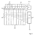
- Fig. 1
- eine schematische Darstellung eines Schaltbilds der Messanordnung,
- Fig. 2
- Signalverläufe über der Zeit,
- Fig. 3
- Signalverläufe über der Zeit bei unterschiedlichen Lichtquellen als Sendelichtquelle und als Referenzlichtquelle,
- Fig. 4
- ein von Fremdlicht beeinflusstes Signal,
- Fig. 5
- eine schematische Darstellung einer Taktverschiebung im Picosekundenbereich,
- Fig. 6
- Taktverläufe bei einer Ausgestaltung gemäß
Fig. 5 .
- Fig. 1
- a schematic representation of a circuit diagram of the measuring arrangement,
- Fig. 2
- Waveforms over time,
- Fig. 3
- Waveforms over time with different light sources as transmission light source and as reference light source,
- Fig. 4
- a signal influenced by extraneous light,
- Fig. 5
- a schematic representation of a clock shift in the picosecond range,
- Fig. 6
- Clock curves in one embodiment according to
Fig. 5 ,
Ausführliche Beschreibung bevorzugter AusführungsbeispieleDetailed description of preferred embodiments
Die Erfindung wird jetzt beispielhaft unter bezug auf die beigefügten Zeichnungen näher erläutert. Allerdings handelt es sich bei den Ausführungsbeispielen nur um Beispiele, die nicht das erfinderische Konzept auf eine bestimmte Anordnung beschränken sollen. Bevor die Erfindung im Detail beschrieben wird, ist darauf hinzuweisen, dass sie nicht auf die jeweiligen Bauteile der Vorrichtung sowie die jeweiligen Verfahrensschritte beschränkt ist, da diese Bauteile und Verfahren variieren können. Die hier verwendeten Begriffe sind lediglich dafür bestimmt, besondere Ausführungsformen zu beschreiben und werden nicht einschränkend verwendet. Wenn zudem in der Beschreibung oder in den Ansprüchen die Einzahl oder unbestimmte Artikel verwendet werden, bezieht sich dies auch auf die Mehrzahl dieser Elemente, solange nicht der Gesamtzusammenhang eindeutig etwas Anderes deutlich macht.The invention will now be described by way of example with reference to the accompanying drawings. However, the embodiments are only examples that are not intended to limit the inventive concept to a particular arrangement. Before describing the invention in detail, it should be noted that it is not limited to the respective components of the device and the respective method steps, since these components and methods may vary. The terms used herein are intended only to describe particular embodiments and are not intended to be limiting. In addition, if singular or indefinite articles are used in the specification or claims, this also applies to the majority of these elements unless the overall context clearly makes otherwise clear.
Eine Taktsteuerung 1.1, z.B. ein entsprechend programmierter Mikrokontroller, liefert Impulse an mindestens eine Sendelichtquelle 1.8 und eine zweite, in unmittelbarer Nähe des Empfängers befindliche zweite Lichtquelle 1.9, die als Referenzlichtquelle dient. Die Lichtquellen können Leuchtdioden oder Laserdioden oder wahlweise beide Typen gemischt sein. Wenigstens eine der beiden Lichtquellen ist in ihrer Phase und Amplitude um einen bestimmbaren Betrag regelbar. Die Sendelichtquelle 1.8 sendet z.B. alle 10 ms einen Impuls von 100 ns aus. Dieser durchläuft die Lichtstrecke 1.24 und 1.25 zum Objekt und vom Objekt 1.26 zu einem Empfänger wie z.B. der Photodiode 1.10 und würde ohne weitere Maßnahmen als Einzelpuls im Verstärker 1.11 erscheinen. Zur Detektion des Eintreffzeitpunktes würden nun im Stand der Technik die oben genannten Probleme auftreten.A clock control 1.1, e.g. a correspondingly programmed microcontroller, delivers pulses to at least one transmitted light source 1.8 and a second, located in the immediate vicinity of the receiver second light source 1.9, which serves as a reference light source. The light sources may be light emitting diodes or laser diodes or alternatively both types mixed. At least one of the two light sources is adjustable in phase and amplitude by a determinable amount. The transmission light source 1.8 sends e.g. every 10 ms a pulse of 100 ns. This traverses the light path 1.24 and 1.25 to the object and from the object 1.26 to a receiver, such as e.g. the photodiode 1.10 and would appear without further action as a single pulse in the amplifier 1.11. To detect the time of arrival, the problems mentioned above would now occur in the prior art.
Darum wird in der Erfindung zuerst ein Referenzpuls 2.1 gemäß
Das Licht der Sendelichtquelle 1.8 und das Licht der Referenzlichtquelle 1.9 treffen zunächst mit unterschiedlicher Intensität an der Photodiode 1.10 ein. Das bedeutet, der Sendepuls 2.2 wird entweder größer (Empfangssignal 2.8 in
Zunächst wird der Photodiodenverstärker, der Vorverstärker 1.11 während der Zeitdauer aller Pulse durch Steuerleitung 1.30 aktiv geschaltet. Durch diese Maßnahme wird nur der zeitliche Bereich betrachtet, bei dem die Lichtquellen aktiv sind. Verfälschungen des Empfangssignals durch den Lichtanstieg beim ersten Referenzpuls 2.1 und Lichtabfall am Ende des zweiten Referenzpulses 2.3 werden dadurch ausgeschlossen.First, the photodiode amplifier, the preamplifier 1.11 during the duration of all pulses by control line 1.30 is activated. By this measure, only the temporal range is considered, in which the light sources are active. Falsifications of the received signal by the increase in light at the first reference pulse 2.1 and light fall at the end of the second reference pulse 2.3 are thereby excluded.
Eine Zerlegung des Empfangssignals gemäß
Mit den Signalwegschaltern 1.17 und 1.18 werden nun als erstes die Amplitudenunterschiede in den Bereichen A, E mit dem Bereich C verglichen. Dazu schaltet der Signalwegschalter 1.17 den Bereich A, E auf einen ersten Eingang 1.19a eines Vergleichers 1.19. Der Bereich C wird über Invertierstufe 1.12 invertiert zu den Bereichen A+E mit Signalwegschalter 1.18 auf den gleichen Eingang 1.19a des Vergleichers 1.19 gegeben. Der zweite Eingang 1.19b des Vergleichers 1.19 liegt an einer, durch zwei gleiche Widerstände 1.13 gebildeten Mittelwertbildung aus dem direktem und dem invertiertem Signal des Vorverstärkers 1.11. Da sich beide gleich großen Signale wechselspannungsmäßig aufheben, steht somit am Summenpunkt zwischen beiden Widerständen ein reiner Gleichspannungsanteil an. Lediglich eine Gleichspannungsdrift der Ausgangsspannung vom Vorverstärker 1.11 und der Invertierstufe 1.12 teilt sich dem Summenpunkt und somit dem zweiten Eingang 1.19b des Vergleichers mit. Durch diese Maßnahme hebt sich der Einfluss einer temperaturbedingten Gleichspannungsdrift des Verstärkers 1.11 und des Invertierers 1.12 im Vergleicher 1.19 auf.With the signal path switches 1.17 and 1.18, the amplitude differences in the areas A, E are now compared with the area C as the first. For this purpose, the signal path switch 1.17 switches the range A, E to a first input 1.19a of a comparator 1.19. The area C is inverted via inverting stage 1.12 to the areas A + E with signal path switch 1.18 to the same input 1.19a of the comparator 1.19. The second input 1.19b of the comparator 1.19 is located at a, formed by two equal resistances 1.13 averaging of the direct and the inverted signal of the preamplifier 1.11. Since both equally large signals cancel each other by alternating voltages, a pure DC voltage component is thus present at the summation point between the two resistors. Only a DC drift of the output voltage from the preamplifier 1.11 and the inverter 1.12 is divided into the summing point and thus the second input 1.19b of the comparator. As a result of this measure, the influence of a temperature-induced DC drift of the amplifier 1.11 and of the inverter 1.12 in the comparator 1.19 is canceled out.
Der Vergleicher 1.19 selbst kann als hochverstärkender Operationsverstärker mit Integration 1.31 des Eingangssignals ausgeführt werden.The comparator 1.19 itself can be implemented as a high-gain operational amplifier with integration 1.31 of the input signal.
Aufgabe dieses Vergleichers 1.19 ist es, eine noch so kleine Differenz der Eingangswerte zu detektieren und am Ausgang 1.19c als Regelwert 1.29 zur Verfügung zu stellen. Dieser Regelwert kann für die Erfassung von Änderungen an oder infolge des Objekts ausgewertet werden und dient damit z.B. zur Erfassung von Position, Lage und Bewegung des Objekts 1.26.The task of this comparator 1.19 is to detect even the smallest difference of the input values and to provide them at the output 1.19c as control value 1.29. This control value can be evaluated for the detection of changes to or as a result of the object and thus serves e.g. for detecting the position, position and movement of the object 1.26.
Die Beschaltungen 1.31 der Vergleicher 1.16, 1.19 und 1.22 entsprechen einer integrierenden "Sample and Hold" Funktion. Für den Vergleicher 1.19 z.B. bedeutet dies, dass der Mittelwert des mit dem Signalwegschalter 1.17 bzw. 1.18 abgetasteten Signals bis zum nächsten Taktzyklus gespeichert wird.The circuits 1.31 of the comparators 1.16, 1.19 and 1.22 correspond to an integrating "sample and hold" function. For the comparator 1.19 e.g. this means that the mean value of the signal sampled with the signal path switch 1.17 or 1.18 is stored until the next clock cycle.
Somit werden im Vergleicher 1.19 die Amplitudenwerte der Referenzpulse 2.1 und 2.3 mit den Amplitudenwerten des Sendepulses 2.2 verglichen. Ein Unterschied zwischen beiden Werten führt zu einer Regelspannung 1.29 am Ausgang 1.19c des Vergleichers 1.19. Mit dieser Regelspannung wird mindestens eine der beiden Lichtquellen 1.8 und 1.9 in ihrer Amplitude so lange nachgeregelt, bis kein Unterschied der Eingangsspannungen am Vergleicher 1.19 anliegt oder zumindest minimal wird. Im Ausführungsbeispiel wird die Referenzlichtquelle 1.9 über die Amplitudenregelung 1.6 direkt geregelt, während die Sendelichtquelle 1.8 über die Amplitudenregelung 1.7 und den Inverter 1.12 invers geregelt wird.Thus, in the comparator 1.19, the amplitude values of the reference pulses 2.1 and 2.3 are compared with the amplitude values of the transmit pulse 2.2. A difference between the two values leads to a control voltage 1.29 at the output 1.19c of the comparator 1.19. With this control voltage, at least one of the two light sources 1.8 and 1.9 is readjusted in its amplitude until no difference of the input voltages at the comparator 1.19 is present or at least minimal. In the exemplary embodiment, the reference light source 1.9 is controlled directly via the amplitude control 1.6, while the transmission light source 1.8 is controlled inversely via the amplitude control 1.7 and the inverter 1.12.
Bei schwacher Reflexion am Objekt 1.26 ist die Sendestufe z.B. auf hohe Leistung geregelt, während die Referenzlichtquelle 1.9 so weit abgeregelt wird, bis im Empfänger 1.10 die Referenzpulse 2.1, 2.3 gleich groß wie der Sendepuls 2.2 erscheinen. Lassen wir die Zeitverschiebung durch die Lichtstrecken 1.24 und 1.25 außer Betracht, ist der Gesamt-Sendepuls im Empfangssignal, bestehend aus erstem Referenzsignal 2.1, dem Sendesignal 2.2 und dem zweiten Referenzsignal 2.3 nicht als solcher sichtbar. Er ist sozusagen "verschwunden".With weak reflection at the object 1.26 the transmission step is e.g. regulated to high power, while the reference light source 1.9 is adjusted so far until the reference pulses 2.1, 2.3 appear the same as the transmission pulse 2.2 in the receiver 1.10. If we omit the time shift due to the light paths 1.24 and 1.25, the total transmit pulse in the receive signal consisting of the first reference signal 2.1, the transmit signal 2.2 and the second reference signal 2.3 is not visible as such. He has "disappeared", so to speak.
Durch diese Maßnahme ist zwar der Sendepuls so in eine zweite Signalumgebung eingebettet, dass er nicht mehr sichtbar ist, jedoch soll im Falle einer Lichtlaufzeitmessung die Zeit bestimmt werden, die dieser Puls auf den Lichtstrecken 1.24 und 1.25 zurückgelegt hat. Angenommen, die Lichtstrecke 1.24 ist 15 cm lang, hin und zurück also 30 cm. Bei einer Lichtlaufzeit von gerundet 300.000 km/s braucht der Puls eine Nanosekunde. Der Puls kommt im Empfänger als mit einer "Verspätung" von einer Nanosekunde an.By this measure, although the transmission pulse is embedded in a second signal environment so that it is no longer visible, but should be determined in the case of a light time measurement, the time that this pulse has traveled on the light paths 1.24 and 1.25. Suppose that the 1.24 light range is 15 cm long, and thus 30 cm back and forth. With a light runtime of 300,000 km / s, the pulse takes a nanosecond. The pulse arrives in the receiver as having a "delay" of one nanosecond.
Diesen Zustand zeigt in
Eine "langsame" Photodiode und ein "langsamer" Vorverstärker können diesen kurzen Puls nicht mehr auflösen. Da zusätzlich noch die Anstiegszeiten bei handelsüblichen Leuchtdioden und Treiberstufen in C-MOS Technologie durchaus länger als eine Nanosekunde sind, würde im besten Falle ein stark verschliffener und in seiner Amplitude schlecht bestimmbarer Puls am Ausgang des Vorverstärkers 1.11 erscheinen.A "slow" photodiode and a "slow" preamp can not resolve this short pulse. Since, in addition, the rise times for commercially available light-emitting diodes and driver stages in C-MOS technology are definitely longer than a nanosecond, in the best case a strongly attenuated pulse whose amplitude would be difficult to determine would appear at the output of preamplifier 1.11.
Wird aber nach der hier beschriebenen Methode die Laufzeit des Lichtsignals bestimmt, ist man nicht mehr auf eine genaue Messung des empfangenen Lichtpulses angewiesen. Vielmehr ist es sogar von Vorteil, wenn der empfangene Puls durch eine Begrenzung der Photodioden- bzw. Vorverstärkerbandbreite "verschliffen" wird. Die Energie des Pulses geht beim Verschleifen, d.h. bei Durchgang durch einen Verstärker mit reduzierter Bandbreite, nicht verloren. Aus einem Puls von einer Nanosekunde und einer Pulshöhe von z.B. 10 mV wird dann z.B. eine Pulshöhe von 10 Mikrovolt, jedoch mit einer Länge von 1000 Nanosekunden. Dieser "kleine", aber lange Puls lässt sich nun problemlos mit C-MOS Technologie verstärken. Bei einer Verstärkung von 80dB ergibt sich dann eine Pulshöhe von 100 mV. Der Photodiodenverstärker 1.11 kann auch als hochverstärkender Begrenzerverstärker ausgeführt sein. Die zeitlich präzise Zuordnung des Empfangspulses 2.5 geht zwar verloren, wird aber in dem hier beschrieben Verfahren auch nicht benötigt.However, if the transit time of the light signal is determined by the method described here, one is no longer dependent on an accurate measurement of the received light pulse. Rather, it is even advantageous if the received pulse is "ground" by limiting the photodiode or preamplifier bandwidth. The energy of the pulse goes through the grinding, i. when passing through an amplifier with reduced bandwidth, not lost. From a pulse of one nanosecond and a pulse height of e.g. 10 mV is then applied e.g. a pulse height of 10 microvolts, but with a length of 1000 nanoseconds. This "small" but long pulse can now be easily amplified with C-MOS technology. At a gain of 80dB, the result is a pulse height of 100 mV. The photodiode amplifier 1.11 can also be designed as a high-gain limiter amplifier. The temporally precise assignment of the received pulse 2.5 is indeed lost, but is not needed in the method described here.
Das Signal 2.9 in
Der zweite Eingang 1.16b des Vergleichers 1.16 liegt an einer durch zwei gleiche Widerstände 1.13 gebildeten Mittelwertbildung aus dem direktem und dem invertiertem Signal des Vorverstärkers 1.11. Da sich beide gleich großen Signale wechselspannungsmäßig aufheben, steht somit am Summenpunkt zwischen beiden Widerständen ein reiner Gleichspannungsanteil an. Lediglich eine Gleichspannungsdrift der Ausgangsspannung von Vorverstärker 1.11 und Invertierstufe 1.12 teilt sich dem Summenpunkt und somit dem zweiten Eingang 1.16b des Vergleichers 1.16 mit. Durch diese Maßnahme hebt sich der Einfluss einer temperaturbedingten Gleichspannungsdrift des Verstärkers 1.11 und des Invertierers 1.12 im Vergleicher 1.16 auf. Der Vergleicher kann identisch wie der Vergleicher 1.19 ausgeführt sein, also als hochverstärkender Operationsverstärker mit Integration des Eingangssignals. Die Ausführung der hier beschriebenen Vergleicher kann auch andersartig sein, wesentlich ist nur, das sie zwei Signale mit einander vergleichen und dabei eine hohe Verstärkung aufweisen. Ein Unterschied zwischen beiden Eingangswerten des Vergleichers 1.16 führt zu einer Regelspannung 1.27 am Ausgang des Vergleichers 1.16.The second input 1.16b of the comparator 1.16 is located at an averaging formed by two equal resistances 1.13 from the direct and the inverted signal of the preamplifier 1.11. Since both equally large signals cancel each other by alternating voltages, a pure DC voltage component is thus present at the summation point between the two resistors. Only a DC drift of the output voltage of preamplifier 1.11 and inversion stage 1.12 shares the sum point and thus the second input 1.16b of the comparator 1.16. As a result of this measure, the influence of a temperature-induced DC drift of the amplifier 1.11 and of the inverter 1.12 in the comparator 1.16 is canceled out. The comparator can be identical to the comparator 1.19, ie as a high-gain operational amplifier with integration of the input signal. The execution of the comparators described here can also be different, it is only essential that they compare two signals with each other while having a high gain. A difference between the two input values of comparator 1.16 leads to a control voltage 1.27 at the output of comparator 1.16.
Im Ausführungsbeispiel werden die Informationen aus den Abschnitten B und D unmittelbar miteinander verglichen werden, wie dies auch in
Die Regelspannung 1.27 wird an eine Regelspannungsverarbeitung 1.2 gegeben. In Abhängigkeit von der Regelspannung 1.27 verschiebt diese Stufe mit Hilfe der analogen oder digitalen Phasenregelungen 1.3, 1.4, 1.5 die Phasen der Referenzpulse 2.1, 2.3 und des Sendepulses 2.2 so zueinander, das die am Vorverstärker 1.11 anliegenden Pulse in den Zeitabschnitten B und D verschwinden.The control voltage 1.27 is given to a control voltage processing 1.2. Depending on the control voltage 1.27, this stage shifts the phases of the reference pulses 2.1, 2.3 and the transmit pulse 2.2 relative to one another with the aid of the analog or digital phase controls 1.3, 1.4, 1.5 so that the pulses applied to the preamplifier 1.11 disappear in the time periods B and D.
Es reicht aus, wenn nur der Sendepuls 2.2 oder auch nur die Referenzpulse 2.1 und/oder 2.3 in der Zeit verschoben werden, jedoch können selbstverständlich auch Sende und Referenzpulse zueinander verschoben werden. Im beschriebenem Beispiel von einem Abstand des reflektierenden Objektes 1.26 in 15 cm Entfernung müssen die Referenzpulse und der Sendeimpuls um genau eine Nanosekunde zueinander verschoben werden. Dann sind die Taktwechselpulse des Empfangssignals 2.9 gemäß Signal 2.10 ausgelöscht und am Ausgang 1.11 b des Verstärkers 1.11 liegt nur noch das Verstärkerrauschen ohne irgendwelche taktsynchronen Anteile an. In der Additionsstufe 1.23 wird der erste und der zweite Referenzpuls zusammengefasst und der Amplitudenregelung 1.6 zugeführt.It is sufficient if only the transmission pulse 2.2 or only the reference pulses 2.1 and / or 2.3 are shifted in time, but of course also transmission and reference pulses can be shifted to each other. In the described example of a distance of the reflecting object 1.26 in 15 cm distance, the reference pulses and the transmission pulse must be shifted by exactly one nanosecond to each other. Then the timing change pulses of the received signal 2.9 are extinguished according to signal 2.10 and at the output 1.11b of the amplifier 1.11 is only the amplifier noise without any isochronous shares. In the addition stage 1.23, the first and the second reference pulse are combined and fed to the amplitude control 1.6.
In der Regelspannung 1.27 steckt dann die Information der Lichtlaufzeit. Der Wert der Lichtlaufzeit kann aber auch als digitaler Wert erhalten werden.In the control voltage 1.27 is then the information of the light runtime. The value of the light runtime can also be obtained as a digital value.
Eine Bestimmung der Lichtlaufzeit nach dem bis hierhin beschriebenem Verfahren hat den Vorteil sehr hoher Detektionsempfindlichkeit bei einem sehr hohem Dynamikbereich der Reflexion. Das beschriebene Verfahren arbeitet ggf. auch mit nur einem Referenzpuls. Schnell sich ändernden Fremdlichteinflüsse können dann jedoch zu kurzzeitigen Messwertfehlern führen.A determination of the light transit time according to the method described so far has the advantage of very high detection sensitivity with a very high dynamic range of the reflection. If necessary, the method described also works with only one reference pulse. However, rapidly changing extraneous light influences can then lead to short-term measured value errors.
Selbstverständlich können auch andere Pulsfolgen als im Ausführungsbeispiel dargestellt, verwendet werden. So kann auch der z.B. nur eine Referenzpuls zwischen zwei Sendepulse eingebettet werden.Of course, other pulse sequences as shown in the embodiment, can be used. So also the e.g. only one reference pulse can be embedded between two transmission pulses.
Bei der Verwendung von Lichtquellen mit unterschiedlichen Reaktionszeiten kann das Empfangssignal in den Zeitabschnitten B und D nicht präzise ausgelöscht werden. Dieser Unterschied in den Anstiegs- und Abfallzeiten entsteht z.B. bei Leuchtdioden verschiedener Chargen oder bei Verwendung einer Laserdiode als Sender und aus Kostengründen einer LED als Referenzlichtquelle.
Bei starker Reflexion (Retroreflektor in unmittelbarer Nähe des Sensors) und einem starken Fremdlichteinfluss (Sonnenlicht mit 100 klx direkt in die Photodiode) können auf Grund der dann entstehenden Unlinearitäten in der Photodiode und dem nicht vollständig ausgelöschtem Signal Messfehler entstehen. Um dies zu verhindern, werden mittels eines weiteren Vergleichers 1.22 die Taktabschnitte A,C und E mit dem Taktabschnitten B und D verglichen. Dazu schaltet der Signalwegschalter 1.20 die Taktabschnitte A,C,E auf einen Eingang 1.22a des Vergleichers 1.22, während der Signalwegschalter 1.21 die Taktabschnitte B,D auf den anderen Eingang 1.22b schaltet. Der Ausgang 1.22c des Vergleichers 1.22 ist mit der Regelspannungsverarbeitung 1.2 verbunden.With strong reflection (retroreflector in the immediate vicinity of the sensor) and a strong influence of extraneous light (sunlight with 100 klx directly into the photodiode), measurement errors can occur due to the resulting non-linearities in the photodiode and the signal which is not completely extinguished. In order to prevent this, the clock sections A, C and E are compared with the clock sections B and D by means of a further comparator 1.22. For this purpose, the signal path switch 1.20 switches the clock sections A, C, E to an input 1.22a of the comparator 1.22, while the signal path switch 1.21 switches the clock sections B, D to the other input 1.22b. The output 1.22c of the comparator 1.22 is connected to the control voltage processing 1.2.
Detektiert der Vergleicher 1.22 einen Unterschied in den Taktabschnitten A,C,E gegenüber B,D, so wirkt die Regelspannungsverarbeitung 1.2 so auf die Phasenregelung ein, das z.B. der Sendepuls so lange verlängert oder verkürzt wird, bis der Restfehler 3.5 vollkommen ausgelöscht wird und wieder nur das Verstärkerrauschen ohne taktsynchrone Anteile am Photodiodenverstärker 1.11 ansteht. Dabei ist es gleichgültig, ob der Sendepuls oder die Referenzpulse in der zeitlichen Länge beeinflusst oder die Referenzpulse in ihrer Lage verschoben werden. Alle drei Regelungen, also Amplitude, Zeitverschiebung und Kompensation der Reaktionszeit können gleichzeitig aktiv sein, ohne sich gegenseitig zu stören.If the comparator 1.22 detects a difference in the clock sections A, C, E compared to B, D, the control voltage processing 1.2 thus acts on the phase control, which is e.g. the transmission pulse is extended or shortened until the residual error 3.5 is completely extinguished and again only the amplifier noise is present without isochronous portions of the photodiode amplifier 1.11. It does not matter whether the transmit pulse or the reference pulses are influenced in the time length or the reference pulses are shifted in their position. All three regulations, ie amplitude, time shift and compensation of the reaction time can be active at the same time, without disturbing each other.
Um einen digitalen Wert für die Lichtlaufzeit zu erhalten, kann dafür eine digitale Signalverzögerung eingesetzt werden. Eine gewünschte Auflösung von z.B. 1.5 mm bedeutet dann eine Schrittweite von 10 Picosekunden. Entsprechend dazu müsste dann die Taktrate eines möglichen Mikroprozessors theoretisch 100 Gigahertz betragen, eine Taktfrequenz die z.Zt. noch nicht möglich ist. Eine Lösung zur Taktverschiebung im Picosekundenbereich zeigt
Die Verzögerungszeit eines Gatters ist Temperatur- und Versorgungsspannungs-abhängig. Um dieses Problem zu umgehen, wird der Takt 5.11 nach Durchlaufen aller Gatter in einem Phasenvergleicher 5.2 mit dem Eingangstakt 5.4 verglichen. Bei einer entsprechenden Anzahl von Gattern kann dann der Takt, der alle Gatter durchlief und der Eingangstakt 5.4 wieder gleiche Phase aufweisen. Im Phasenvergleicher 5.2 wird ein Phasenunterschied detektiert und als Regelspannung Gatterlaufzeit 5.9 ausgegeben. Diese steuert die Verzögerungszeit der Gatter. Im einfachsten Fall wird zur Steuerung der Signalverzögerung die Versorgungsspannung der Gatter beeinflusst. Es kann auch eines der beiden Eingangssignale des Phasenvergleichers 5.2 invertiert werden (5.10), in diesem Fall wird nur die Hälfte der Gatter benötigt. Dies verdeutlicht
Der über die Photodiode 1.10, Vorverstärker 1.11, Signalwegschalter 1.14 und 1.15, Vergleicher 1.16, Regelspannungsverarbeitung 1.2, Phasenregelungen 1.3, 1.4, und 1.5 und Lichtquellen 1.8 und 1.9 geschlossene Regelkreis sorgt selbstständig für eine Verschiebung der Referenz- bzw. Sendephase um genau den Wert der Lichtlaufzeit in der Strecke 1.24 und 1.25. Somit ist eine einfache Bestimmung der Lichtlaufzeit und damit des Abstandes zu einem reflektierenden Objekt 1.26 gegeben.The via the photodiode 1.10, preamplifier 1.11, Signalwegschalter 1.14 and 1.15, comparator 1.16, control voltage processing 1.2, phase control 1.3, 1.4, and 1.5 and light sources 1.8 and 1.9 closed loop automatically ensures a shift of the reference or send phase by exactly the value of Light time in the track 1.24 and 1.25. Thus, a simple determination of the light transit time and thus the distance to a reflective object 1.26 is given.
Es versteht sich von selbst, dass diese Beschreibung verschiedensten Modifikationen, Änderungen und Anpassungen unterworfen werden kann, die sich im Bereich von Äquivalenten zu den anhängenden Ansprüchen bewegen.
Claims (15)
- Method for determining a distance to a retroreflective object with the steps:- transmitting a transmitted signal (2.2) clocked by a clock control (1.1) from at least one transmitting light source (1.8) into at least one light path (1.24, 1.25) via the object (1.26) to at least one receiver (1.10) to detect the change in the transmitted signal resulting from the object (1.26),- receiving the transmitted signal (2.2) coming from the light path (1.24, 1.25) by means of the at least one receiver (1.10) and converting the received signal resulting from the transmitted signal at the receiver (1.10) into an electrical signal (2.5),- transmitting at least one reference signal (2.1, 2.3) clocked by the clock control (1.1) from at least one reference light source (1.9) into at least one further light path to the at least one receiver (1.10),- receiving the reference signal (2.1, 2.3) coming from the further light path by means of the at least one receiver (1.10) and converting the received signal resulting from the reference signal at the receiver (1.10) into an electrical reference signal (2.4, 2.6),- evaluating the electrical signal (2.5) and the electrical reference signal (2.4, 2.6) in at least one comparator (1.19) to determine the distance to the object (1.26),- wherein the electrical signal (2.5) resulting from the transmitted signal (2.2) integrated over at least a sub-section of the transmitted signal is respectively compared with at least one electric reference signal (2.4, 2.6) resulting from the reference signal (2.1, 2.3), which at least one electric reference signal is adjacent in time, staggered in time due to the differing light paths and integrated over at least one sub-section of the reference signal,- at the output (1.19c) of the comparator (1.19) a control value (1.29) is generated to regulate the amplitude values of the transmitted signal (2.2) and/or the reference signal (2.1, 2.3), as a result of which control value the amplitude of the electrical signal (2.5) and the amplitude of the electrical reference signal (2.4, 2.6) are substantially equal in magnitude at least at the inputs (1.19a, 1.19b) of the comparator (1.19), and- in the thus stabilised state the amplitude of the clock pulse change signal, which occurs during the clock pulse change and corresponds to the light transit time from the transmitting light source (1.8) to the object (1.26) and to the receiver (1.10), between the electrical signal (2.5) and the electrical reference signal (2.4, 2.6) and/or the electrical reference signal (2.4, 2.6) and the electrical signal (2.5) is determined, and- the amplitude of the clock pulse change signals in relation to one another or the amplitude of the clock pulse change signal compared to an amplitude independent of this light transit time is determined as difference value (1.27) in a further comparator (1.16) and eliminated or at least minimised by means of a regulator (1.2).
- Method for determining a distance to a retroreflective object with the steps:- transmitting a transmitted signal (2.2) clocked by a clock control (1.1) from at least one transmitting light source (1.8) into at least one light path (1.24, 1.25) via the object (1.26) to at least one receiver (1.10) to detect the change in the transmitted signal resulting from the object (1.26),- receiving the transmitted signal (2.2) coming from the light path (1.24, 1.25) by means of the at least one receiver (1.10) and converting the received signal resulting from the transmitted signal at the receiver (1.10) into an electrical signal (2.5),- forwarding an electrical reference signal clocked by the clock control (1.1),- evaluating the electrical signal (2.5) and the electrical reference signal (2.4, 2.6) in at least one comparator (1.19) to determine the distance to the object (1.26),- wherein the electrical signal (2.5) resulting from the transmitted signal (2.2) integrated over at least a sub-section of the transmitted signal is respectively compared with at least one electric reference signal (2.4, 2.6), which is adjacent in time, staggered in time due to the light path and integrated over at least one sub-section of the electrical reference signal,- at the output (1.19c) of the comparator (1.19) a control value (1.29) is generated to regulate the amplitude values of the transmitted signal (2.2) and/or the electrical reference signal, as a result of which control value the amplitude of the electrical signal (2.5) and the amplitude of the electrical reference signal (2.4, 2.6) are substantially equal in magnitude at least at the inputs (1.19a, 1.19b) of the comparator (1.19), and- in the thus stabilised state the amplitude of the clock pulse change signal, which occurs during the clock pulse change and corresponds to the light transit time from the transmitting light source (1.8) to the object (1.26) and to the receiver (1.10), between the electrical signal (2.5) and the electrical reference signal (2.4, 2.6) and/or the electrical reference signal (2.4, 2.6) and the electrical signal (2.5) is determined, and- the amplitude of the clock pulse change signals in relation to one another or the amplitude of the clock pulse change signal compared to an amplitude independent of this light transit time is determined as difference value (1.27) in a further comparator (1.16) and eliminated or at least minimised by means of a regulator (1.2).
- Method according to claim 1 or 2, characterised in that the electrical reference signal at the input of the comparator (1.19) is formed by the mean value of the electrical reference signals of at least two reference signals (2.4, 2.6) in pulse form, of which one is emitted before and one is emitted after the transmitted signal in pulse form.
- Method according to one of the preceding claims, characterised in that the amplitude value independent of this light transit time is the amplitude value at the preamplifier (1.11) when the electrical signal (2.5) and the electrical reference signal (2.4, 2.6) at the inputs (1.19a, 19b) of the comparator (1.19) are substantially equal in magnitude.
- Method according to one of the preceding claims, characterised in that the difference value (1.27) is changed by means of the regulator (1.2) to regulate the phase of the transmitted signal (2.2) and the reference signal (2.1, 2.3) until the difference value (1.27) is minimal, preferably zero, wherein the adjusted change in the case of a minimal difference value corresponds to the light transit time.
- Method according to one of the preceding claims, respectively, according to one of the claims 1 or 3 to 5, as far as the reference light source (1.9) is concerned, characterised in that, if the electrical signal (2.5) and the electrical reference signal (2.4, 2.6) at the inputs (1.19a, 1.19b) of the comparator (1.19) are substantially equal in magnitude, only amplifier noise without clock-synchronous alternating components from the transmitting light source (1.8) and/or reference light source (1.9) is possibly present at the output (1.19c) of the comparator (1.19).
- Method according to one of the preceding claims, , respectively, according to one of the claims 1 or 3 to 6, as far as the reference light source (1.9) is concerned, characterised in that to compensate different reaction times between the transmitting light source (1.8) and the reference light source (1.9) the sections (A,C,E), which contain no clock pulse change signal, are compared with the sections (B,D), which contain a clock pulse change signal, with one another in a further comparator (1.22), and that in the case of a difference at the output (1.22c) of the comparator (1.22) the transmitted signal (2.2) and/or the reference signal (2.1, 2.3) or the forwarded electrical reference signal are lengthened or shortened until the difference (3.5) is eliminated.
- Method according to one of the preceding claims, characterised in that for digital signal delay a number of gates (5.1) tappable by switches (5.8) are provided, wherein the switch is selected in dependence on the difference value (1.27), wherein additionally preferably the clock control (1.1) generates a clock pulse, and after passing through all the gates (5.1), which corresponds to the time of at least a half or a whole clock pulse period, the clock pulse (5.11) is compared with the input clock pulse (5.4) in a phase comparator (5.2) to identify a phase difference, and that any phase difference present regulates the delay time of the gates (5.1) preferably by means of a supply voltage of the gate.
- Device for determining a distance to a retroreflective object (1.26) with:- a clock control (1.1),- at least one transmitting light source (1.8) for transmitting a transmitted signal (2.2) clocked by the clock control (1.1) into at least one light path (1.24, 1.25) via the object (1.26) to at least one receiver (1.10) to determine the change in the transmitted signal resulting from the object (1.26),- at least one reference light source (1.9) for transmitting a reference signal (2.1, 2.3) clocked by the clock control (1.1) into at least one further light path to the at least one receiver (1.10),- the at least one receiver (1.10) for receiving the transmitted signal (2.2) coming from the light path (1.24, 1.25) and the reference signal (2.1, 2.3) coming from the further light path and for converting the received signal resulting from the transmitted signal (2.2) at the receiver (1.10) into an electrical signal (2.5) and the received signal resulting from the reference signal (2.1, 2.3) at the receiver (1.10) into an electrical reference signal (2.4, 2.6),- at least one comparator (1.19) for comparing the electrical signal (2.5) and the electrical reference signal (2.4, 2.6) to generate a comparative value (1.29) at the output of the comparator (1.19),- an evaluation unit for evaluating the comparative value to determine a distance to the object (1.26),- wherein a control unit is provided, which controls the clock control (1.1) and signal path switches (1.17, 1.18) to respectively integrate the electrical signal (2.5) present over at least one sub-section of the transmitted signal (2.2) and to integrate the at least one electrical reference signal (2.4, 2.6), which is adjacent in time to the transmitted signal, and is staggered in time due to the differing light paths and integrated over at least one sub-section of the electrical reference signal,- at least one regulator (1.6) is provided, which is used to regulate the amplitude values of the transmitted signal (2.2) and/or the reference signal (2.1, 2.3) so that the amplitude of the electrical signal (2.5) and the amplitude of the electrical reference signal (2.4, 2.6) are substantially equal in magnitude at least at the inputs (1.19a, 1.19b) of the comparator (1.19),- in the thus stabilised state means for detecting the amplitude of at least one clock pulse change signal are provided, which occurs during the clock pulse change and corresponds to the light transit time from the transmitting light source (1.8) to the object (1.26) and to the receiver (1.10), between the electrical signal (2.5) and the electrical reference signal (2.4, 2.6) and/or the electrical reference signal (2.4, 2.6) and the electrical signal (2.5),- a further comparator (1.16) is provided to determine a difference value (1.27) between the amplitudes of the clock pulse change signals in relation to one another or the amplitude of the clock pulse change signal compared to an amplitude value independent of this light transit time, and- a regulator (1.2) is provided, which eliminates or at least minimises the difference value (1.27).
- Device for determining a distance to a retroreflective object (1.26) with:- a clock control (1.1),- at least one transmitting light source (1.8) for transmitting a transmitted signal (2.2) clocked by the clock control (1.1) into at least one light path (1.24, 1.25) via the object (1.26) to at least one receiver (1.10) to determine the change in the transmitted signal resulting from the object (1.26),- the at least one receiver (1.10) for receiving the transmitted signal (2.2) coming from the light path (1.24, 1.25) and for converting the received signal as a result of the transmitted signal (2.2) at the receiver (1.10) into an electrical signal (2.5),- a reference path for forwarding an electrical reference signal (2.4, 2.6),- at least one comparator (1.19) for comparing the electrical signal (2.5) and the electrical reference signal (2.4, 2.6) to generate a comparative value (1.29) at the output of the comparator (1.19),- an evaluation unit for evaluating the comparative value to determine a distance to the object (1.26),- wherein a control unit is provided, which controls the clock control (1.1) and signal path switches (1.17, 1.18) to respectively integrate an electrical signal (2.5) present over at least one sub-section of the transmitted signal (2.2) and to integrate the at least one electrical reference signal (2.4, 2.6), which is adjacent in time to the transmitted signal, staggered in time and integrated over at least one sub-section of the electrical reference signal,- at least one regulator (1.6) is provided, which is used to regulate the amplitude values of the transmitted signal (2.2) and/or the electrical reference signal (2.1, 2.3) so that the amplitude of the electrical signal (2.5) and the amplitude of the electrical reference signal (2.4, 2.6) are substantially equal in magnitude at least at the inputs (1.19a, 1.19b) of the comparator (1.19),- in the thus stabilised state means for detecting the amplitude of at least one clock pulse change signal are provided, which occurs during the clock pulse change and corresponds to the light transit time from the transmitting light source (1.8) to the object (1.26) and to the receiver (1.10), between the electrical signal (2.5) and the electrical reference signal (2.4, 2.6) and/or the electrical reference signal (2.4, 2.6) and the electrical signal (2.5),- a further comparator (1.16) is provided to determine a difference value (1.27) between the amplitudes of the clock pulse change signals in relation to one another or the amplitude of the clock pulse change signal compared to an amplitude value independent of this light transit time, and- a regulator (1.2) is provided, which eliminates or at least minimises the difference value (1.27).
- Device according to claim 9 or 10, characterised in that a mean value former is provided to form a mean value of the electrical reference signals (2.4, 2.6) resulting from at least two reference signals (2.1, 2.3) in pulse form at an input (1.19b) of the comparator (1.19), of which reference signals one is emitted before and one is emitted after the transmitted signal (2.2) in pulse form.
- Device according to claim 11, characterised in that the amplitude value independent of this light transit time is the amplitude value at the preamplifier (1.11) when the electrical signal (2.5) and the electrical reference signal (2.4, 2.6) at the inputs (1.19a, 1.19b) of the comparator (1.19) are substantially equal in magnitude.
- Device according to one of claims 9 to 12, characterised in that the regulator (1.2) is provided to regulate the phase of the transmitted signal (2.2) and the reference signal (2.1, 2.3) by influencing and minimising the difference value (1.27) preferably to zero, wherein the delay adjusted in the case of a minimal difference value corresponds to the light transit time.
- Device according to one of claims 9 to 13, characterised in that a further comparator (1.22) is provided to compensate different reaction times between the transmitting light source (1.8) and the reference light source (1.9), which comparator compares sections (A,C,E), which contain no clock pulse change signal, with sections (B,D), which contain a clock pulse change signal, and
that a regulator (1.2) is provided, which lengthens or shortens the transmitted signal (2.2) and/or the reference signal (2.1, 2.3) or the forwarded electrical reference signal in the case of a difference at the output (1.22c) of the further comparator (1.22) until the difference (3.5) is eliminated. - Device according to one of claims 9 to 14, characterised in that for digital signal delay a number of gates (5.1) tappable by means of switches (5.8) are provided, wherein the switch is selected in dependence on the difference value (1.27), wherein preferably a phase comparator (5.2) is provided, which compares the input clock pulse (5.4) of the clock control (1.1) with the clock pulse (5.11), which is present after passing through all the gates (5.1) and corresponds to the time of at least a half or a whole clock pulse period, to determine a phase difference, and that a regulator (1.2) is provided, which if any phase difference is present regulates the delay time of the gates (5.1) preferably by means of a supply voltage of the gate.
Applications Claiming Priority (2)
| Application Number | Priority Date | Filing Date | Title |
|---|---|---|---|
| DE102007005187A DE102007005187B4 (en) | 2007-01-29 | 2007-01-29 | Method and device for determining a distance to a retroreflective object |
| PCT/EP2008/000615 WO2008092611A1 (en) | 2007-01-29 | 2008-01-28 | Method and device for determining the distance to a retroreflective object |
Publications (2)
| Publication Number | Publication Date |
|---|---|
| EP2118680A1 EP2118680A1 (en) | 2009-11-18 |
| EP2118680B1 true EP2118680B1 (en) | 2015-11-18 |
Family
ID=39433844
Family Applications (1)
| Application Number | Title | Priority Date | Filing Date |
|---|---|---|---|
| EP08707321.9A Not-in-force EP2118680B1 (en) | 2007-01-29 | 2008-01-28 | Method and device for determining the distance to a retroreflective object |
Country Status (5)
| Country | Link |
|---|---|
| US (1) | US8405821B2 (en) |
| EP (1) | EP2118680B1 (en) |
| JP (1) | JP5688900B2 (en) |
| DE (1) | DE102007005187B4 (en) |
| WO (1) | WO2008092611A1 (en) |
Families Citing this family (30)
| Publication number | Priority date | Publication date | Assignee | Title |
|---|---|---|---|---|
| DE102009058817A1 (en) | 2009-12-18 | 2010-08-05 | Daimler Ag | System for dimensionally stable roll-hemming of component i.e. sheet component, of industrial robot, has sensor device including non-contact measuring sensor to detect path of folding edge |
| US20120200422A1 (en) * | 2011-02-09 | 2012-08-09 | Baker Hughes Incorporated | Use of Digital Transport Delay to Improve Measurement Fidelity in Swept-Wavelength Systems |
| EP2602635B1 (en) | 2011-12-06 | 2014-02-19 | ELMOS Semiconductor AG | Method for measuring a transfer route by means of compensating amplitude measurement and delta-sigma method and device for performing the method |
| EP2631674A1 (en) | 2012-02-23 | 2013-08-28 | ELMOS Semiconductor AG | Method and sensor system for measuring the properties of a transfer segment of a measuring system between transmitter and recipient |
| EP2653885A1 (en) | 2012-04-18 | 2013-10-23 | ELMOS Semiconductor AG | Method and sensor system for measuring the transfer properties of a transfer segment of a measuring system between transmitter and recipient |
| CN103411630A (en) * | 2012-11-28 | 2013-11-27 | 上海兰宝传感科技股份有限公司 | Intelligent polarized reflection type photoelectric sensor |
| DE102013002676B4 (en) | 2013-02-12 | 2023-06-29 | Elmos Semiconductor Se | Compensated sensor system with a receiver with adjustable sensitivity as a compensating element |
| WO2014131385A1 (en) | 2013-02-27 | 2014-09-04 | Elmos Semiconductor Ag | Multifunctional optical micro sensor system |
| DE102014002486B4 (en) | 2013-02-27 | 2017-10-19 | Elmos Semiconductor Aktiengesellschaft | Compensating optical sensor system |
| WO2014170118A1 (en) * | 2013-04-17 | 2014-10-23 | Mechaless Systems Gmbh | Method for optically measuring distances in the near and far range |
| DE102014002194B4 (en) | 2014-02-12 | 2017-10-19 | Elmos Semiconductor Aktiengesellschaft | Compensating optical microsystem |
| US9606228B1 (en) | 2014-02-20 | 2017-03-28 | Banner Engineering Corporation | High-precision digital time-of-flight measurement with coarse delay elements |
| CN106134105B (en) | 2014-03-20 | 2020-02-04 | 艾里尔大学研究与开发有限公司 | Method and system for controlling signal phase and application equipment thereof |
| EP2924460A1 (en) | 2014-03-25 | 2015-09-30 | ELMOS Semiconductor AG | Sensor system for identifying at least one object in a transmission line by means of a diode |
| EP2924459A1 (en) | 2014-03-25 | 2015-09-30 | ELMOS Semiconductor AG | Sensor system for identifying at least one object in a transmission line |
| EP2924466B1 (en) | 2014-03-25 | 2020-06-03 | Elmos Semiconductor Aktiengesellschaft | Sensor system for identifying at least one object of a transmission line |
| DE102015002282A1 (en) | 2014-05-09 | 2015-11-12 | Elmos Semiconductor Aktiengesellschaft | Device and method for especially three-dimensional optical scanning and measuring of objects and for object recognition by means of light transit time measurement |
| DE102014019172B4 (en) | 2014-12-17 | 2023-12-07 | Elmos Semiconductor Se | Device and method for distinguishing between solid objects, cooking fumes and smoke using a compensating optical measuring system |
| DE102014019773B4 (en) | 2014-12-17 | 2023-12-07 | Elmos Semiconductor Se | Device and method for distinguishing between solid objects, cooking fumes and smoke using the display of a mobile telephone |
| DE102015006174B3 (en) * | 2015-05-08 | 2016-08-11 | Elmos Semiconductor Aktiengesellschaft | Device and method for measuring an optical, capacitive, inductive transmission path |
| US10257014B2 (en) | 2015-10-08 | 2019-04-09 | Ariel-University Research And Development Company Ltd. | Method and system for controlling phase of a signal |
| DE102015015390A1 (en) | 2015-11-18 | 2017-05-18 | Elmos Semiconductor Ag | Simple gesture recognition device |
| DE102015015244A1 (en) | 2015-11-18 | 2017-05-18 | Elmos Semiconductor Aktiengesellschaft | Simple gesture recognition device |
| DE102015015245A1 (en) | 2015-11-18 | 2017-05-18 | Elmos Semiconductor Aktiengesellschaft | Simple gesture recognition device |
| DE102015015248A1 (en) | 2015-11-18 | 2017-05-18 | Elmos Semiconductor Aktiengesellschaft | Simple gesture recognition device |
| DE102015015389A1 (en) | 2015-11-18 | 2017-05-18 | Elmos Semiconductor Ag | Simple gesture recognition device |
| DE102015015246A1 (en) | 2015-11-18 | 2017-05-18 | Elmos Semiconductor Aktiengesellschaft | Simple gesture recognition device |
| DE102017100308B3 (en) | 2016-12-06 | 2018-05-30 | Elmos Semiconductor Aktiengesellschaft | Device and method for measuring an optical, capacitive, inductive transmission path with reduced EMC sensitivity |
| DE102017200803A1 (en) * | 2017-01-19 | 2018-07-19 | Robert Bosch Gmbh | Monitoring device of a lidar system |
| US11092678B2 (en) | 2018-06-21 | 2021-08-17 | Analog Devices, Inc. | Measuring and removing the corruption of time-of-flight depth images due to internal scattering |
Family Cites Families (22)
| Publication number | Priority date | Publication date | Assignee | Title |
|---|---|---|---|---|
| US4523093A (en) * | 1981-09-03 | 1985-06-11 | Excellon Industries | Scanning beam reference and read system |
| DE3316630C2 (en) * | 1983-05-06 | 1985-07-25 | Erwin Sick Gmbh Optik-Elektronik, 7808 Waldkirch | Device for determining the transit time of ultrasonic pulses in a fluid |
| US4788441A (en) * | 1985-12-16 | 1988-11-29 | Acme-Cleveland Corporation | Range finder wherein distance between target and source is determined by measuring scan time across a retroreflective target |
| US6122602A (en) * | 1997-05-02 | 2000-09-19 | Endress + Hauser Gmbh + Co. | Method and arrangement for electromagnetic wave distance measurement by the pulse transit time method |
| JPH1123709A (en) * | 1997-07-07 | 1999-01-29 | Nikon Corp | Distance-measuring device |
| US6043874A (en) * | 1998-04-10 | 2000-03-28 | Spectra Precision, Inc. | System and method for calibrating a laser transmitter |
| DE19830684C1 (en) * | 1998-07-09 | 2000-03-30 | Leuze Electronic Gmbh & Co | Optoelectronic device for determining distance of objects, by averaging distance values for light pulses delayed by time intervals |
| US6055490A (en) * | 1998-07-27 | 2000-04-25 | Laser Technology, Inc. | Apparatus and method for determining precision reflectivity of highway signs and other reflective objects utilizing an optical range finder instrument |
| JP3849324B2 (en) * | 1998-11-02 | 2006-11-22 | 株式会社デンソー | Distance measuring device |
| US7782256B2 (en) * | 1999-03-05 | 2010-08-24 | Era Systems Corporation | Enhanced passive coherent location techniques to track and identify UAVs, UCAVs, MAVs, and other objects |
| DE10022054B4 (en) * | 2000-05-06 | 2006-05-24 | Leuze Electronic Gmbh & Co Kg | Optical distance sensor |
| US6711280B2 (en) * | 2001-05-25 | 2004-03-23 | Oscar M. Stafsudd | Method and apparatus for intelligent ranging via image subtraction |
| EP1576385A2 (en) * | 2002-11-26 | 2005-09-21 | James F. Munro | An apparatus for high accuracy distance and velocity measurement and methods thereof |
| DE10300223B3 (en) * | 2003-01-03 | 2004-06-24 | Gerd Reime | Optoelectronic measuring device with stray light compensation provided by intensity regulation of additional light source |
| CA2516796A1 (en) * | 2003-02-21 | 2004-09-10 | Inesa, Inc. | An apparatus and method for distance measurement with controlled modulation of emitted pulses |
| WO2005054902A1 (en) * | 2003-12-03 | 2005-06-16 | Me-In Gmbh | Circuit for analyzing a reflected signal |
| US7843379B2 (en) * | 2004-11-15 | 2010-11-30 | Nanotron Technologies Gmbh | Symmetrical multi-path method for determining the distance between two transmitter-receivers |
| US7375593B2 (en) * | 2005-01-19 | 2008-05-20 | Paul William Ronald Self | Circuits and methods of generating and controlling signals on an integrated circuit |
| DE102005045993B4 (en) * | 2005-07-29 | 2008-11-13 | Gerd Reime | Method for measuring the time of flight |
| EP1910773B1 (en) * | 2005-07-29 | 2013-03-27 | Gerd Reime | Method and device for distance measurement by means of capacitive or inductive sensors |
| WO2007145839A2 (en) * | 2006-06-05 | 2007-12-21 | Luna Innovations Incorporated | Digital pulsed phase locked loop |
| US7640122B2 (en) * | 2007-11-07 | 2009-12-29 | Institut National D'optique | Digital signal processing in optical systems used for ranging applications |
-
2007
- 2007-01-29 DE DE102007005187A patent/DE102007005187B4/en not_active Expired - Fee Related
-
2008
- 2008-01-28 JP JP2009546698A patent/JP5688900B2/en not_active Expired - Fee Related
- 2008-01-28 US US12/524,904 patent/US8405821B2/en not_active Expired - Fee Related
- 2008-01-28 EP EP08707321.9A patent/EP2118680B1/en not_active Not-in-force
- 2008-01-28 WO PCT/EP2008/000615 patent/WO2008092611A1/en active Application Filing
Also Published As
| Publication number | Publication date |
|---|---|
| WO2008092611A8 (en) | 2009-09-24 |
| US20100182588A1 (en) | 2010-07-22 |
| JP2011511261A (en) | 2011-04-07 |
| DE102007005187A1 (en) | 2008-09-04 |
| EP2118680A1 (en) | 2009-11-18 |
| US8405821B2 (en) | 2013-03-26 |
| DE102007005187B4 (en) | 2008-11-20 |
| WO2008092611A1 (en) | 2008-08-07 |
| JP5688900B2 (en) | 2015-03-25 |
Similar Documents
| Publication | Publication Date | Title |
|---|---|---|
| EP2118680B1 (en) | Method and device for determining the distance to a retroreflective object | |
| EP1913420B1 (en) | Method for light propagation time measurement | |
| EP3098626B1 (en) | Timer circuit and optoelectronic range finder using such a timer circuit | |
| EP2899565B1 (en) | Distance measuring sensor and method for recording and determining the distance of an object | |
| EP1876469B1 (en) | Method and apparatus for optoelectronic contactless distance measuring according to the time of fly principle | |
| EP2088453B1 (en) | Optoelectronic sensor for measuring distance | |
| EP2189814B1 (en) | Optoelectronic sensor and method for measuring distance in accordance with the light-crossing time principle | |
| EP2189805B1 (en) | Optoelectronic sensor and method for measuring distance according to time-of-flight | |
| EP1910773B1 (en) | Method and device for distance measurement by means of capacitive or inductive sensors | |
| EP2041604B1 (en) | Optical distance measuring method and corresponding optical rangefinder | |
| DE102011056963C5 (en) | Measurement of distances according to the signal transit time principle | |
| EP2597482A1 (en) | Device and sensor for distance measurement using the duration of compensated pulses | |
| EP1990657B1 (en) | Optical rangefinder | |
| EP3339901B1 (en) | Laser distance measuring module with adc error compensation by varying sampling times | |
| DE102007013714A1 (en) | Optoelectronic sensor and method for measuring a distance or a range change | |
| EP2189804A1 (en) | Optoelectronic sensor and method for measuring distance according to time-of-flight | |
| EP2558883A1 (en) | Distance measuring device having homogenizing measurement evaluation | |
| DE3419117A1 (en) | OPTOELECTRICAL DISTANCE MEASURING DEVICE WITH A TIME DISCRIMINATOR FOR ACCURATE DETERMINATION OF THE TIMING OF ELECTRICAL IMPULSES | |
| EP1876468B1 (en) | Method and apparatus for optoelectronic contactless distance measuring | |
| DE102012101909B3 (en) | Distance measuring sensor e.g. laser sensor, for detecting and determining distance of object from vehicle, has core providing signal with reduced cycles, where updated value is passed to controller according to multiple cycles | |
| DE102010013751A1 (en) | Device for measuring distance between transceiver and target in industrial application, has evaluating device scanning light pulses with respect to phase shifts, where pulses are transmitted by transmitter at certain pulse repetition rate | |
| DE10236486B4 (en) | Device for non-contact distance measurement | |
| DE102015121578B3 (en) | Transmission apparatus and method for generating a transmission signal | |
| EP2910972B1 (en) | Distance measuring sensor and method for determing the distance from objects in a monitoring zone | |
| DE102012100813B4 (en) | Signal delay measurement |
Legal Events
| Date | Code | Title | Description |
|---|---|---|---|
| PUAI | Public reference made under article 153(3) epc to a published international application that has entered the european phase |
Free format text: ORIGINAL CODE: 0009012 |
|
| 17P | Request for examination filed |
Effective date: 20090824 |
|
| AK | Designated contracting states |
Kind code of ref document: A1 Designated state(s): AT BE BG CH CY CZ DE DK EE ES FI FR GB GR HR HU IE IS IT LI LT LU LV MC MT NL NO PL PT RO SE SI SK TR |
|
| DAX | Request for extension of the european patent (deleted) | ||
| GRAP | Despatch of communication of intention to grant a patent |
Free format text: ORIGINAL CODE: EPIDOSNIGR1 |
|
| RIC1 | Information provided on ipc code assigned before grant |
Ipc: G01S 17/10 20060101ALI20150521BHEP Ipc: G01S 7/497 20060101ALI20150521BHEP Ipc: G01S 7/486 20060101ALI20150521BHEP Ipc: G01S 7/487 20060101AFI20150521BHEP |
|
| INTG | Intention to grant announced |
Effective date: 20150608 |
|
| GRAS | Grant fee paid |
Free format text: ORIGINAL CODE: EPIDOSNIGR3 |
|
| GRAA | (expected) grant |
Free format text: ORIGINAL CODE: 0009210 |
|
| AK | Designated contracting states |
Kind code of ref document: B1 Designated state(s): AT BE BG CH CY CZ DE DK EE ES FI FR GB GR HR HU IE IS IT LI LT LU LV MC MT NL NO PL PT RO SE SI SK TR |
|
| REG | Reference to a national code |
Ref country code: GB Ref legal event code: FG4D Free format text: NOT ENGLISH |
|
| REG | Reference to a national code |
Ref country code: CH Ref legal event code: EP |
|
| REG | Reference to a national code |
Ref country code: AT Ref legal event code: REF Ref document number: 761828 Country of ref document: AT Kind code of ref document: T Effective date: 20151215 |
|
| REG | Reference to a national code |
Ref country code: IE Ref legal event code: FG4D Free format text: LANGUAGE OF EP DOCUMENT: GERMAN |
|
| REG | Reference to a national code |
Ref country code: DE Ref legal event code: R096 Ref document number: 502008013595 Country of ref document: DE |
|
| REG | Reference to a national code |
Ref country code: FR Ref legal event code: PLFP Year of fee payment: 9 |
|
| REG | Reference to a national code |
Ref country code: NL Ref legal event code: MP Effective date: 20160218 |
|
| REG | Reference to a national code |
Ref country code: LT Ref legal event code: MG4D |
|
| PG25 | Lapsed in a contracting state [announced via postgrant information from national office to epo] |
Ref country code: IT Free format text: LAPSE BECAUSE OF FAILURE TO SUBMIT A TRANSLATION OF THE DESCRIPTION OR TO PAY THE FEE WITHIN THE PRESCRIBED TIME-LIMIT Effective date: 20151118 Ref country code: IS Free format text: LAPSE BECAUSE OF FAILURE TO SUBMIT A TRANSLATION OF THE DESCRIPTION OR TO PAY THE FEE WITHIN THE PRESCRIBED TIME-LIMIT Effective date: 20160318 Ref country code: NL Free format text: LAPSE BECAUSE OF FAILURE TO SUBMIT A TRANSLATION OF THE DESCRIPTION OR TO PAY THE FEE WITHIN THE PRESCRIBED TIME-LIMIT Effective date: 20151118 Ref country code: ES Free format text: LAPSE BECAUSE OF FAILURE TO SUBMIT A TRANSLATION OF THE DESCRIPTION OR TO PAY THE FEE WITHIN THE PRESCRIBED TIME-LIMIT Effective date: 20151118 Ref country code: NO Free format text: LAPSE BECAUSE OF FAILURE TO SUBMIT A TRANSLATION OF THE DESCRIPTION OR TO PAY THE FEE WITHIN THE PRESCRIBED TIME-LIMIT Effective date: 20160218 Ref country code: HR Free format text: LAPSE BECAUSE OF FAILURE TO SUBMIT A TRANSLATION OF THE DESCRIPTION OR TO PAY THE FEE WITHIN THE PRESCRIBED TIME-LIMIT Effective date: 20151118 Ref country code: LT Free format text: LAPSE BECAUSE OF FAILURE TO SUBMIT A TRANSLATION OF THE DESCRIPTION OR TO PAY THE FEE WITHIN THE PRESCRIBED TIME-LIMIT Effective date: 20151118 |
|
| PG25 | Lapsed in a contracting state [announced via postgrant information from national office to epo] |
Ref country code: PT Free format text: LAPSE BECAUSE OF FAILURE TO SUBMIT A TRANSLATION OF THE DESCRIPTION OR TO PAY THE FEE WITHIN THE PRESCRIBED TIME-LIMIT Effective date: 20160318 Ref country code: SE Free format text: LAPSE BECAUSE OF FAILURE TO SUBMIT A TRANSLATION OF THE DESCRIPTION OR TO PAY THE FEE WITHIN THE PRESCRIBED TIME-LIMIT Effective date: 20151118 Ref country code: FI Free format text: LAPSE BECAUSE OF FAILURE TO SUBMIT A TRANSLATION OF THE DESCRIPTION OR TO PAY THE FEE WITHIN THE PRESCRIBED TIME-LIMIT Effective date: 20151118 Ref country code: LV Free format text: LAPSE BECAUSE OF FAILURE TO SUBMIT A TRANSLATION OF THE DESCRIPTION OR TO PAY THE FEE WITHIN THE PRESCRIBED TIME-LIMIT Effective date: 20151118 Ref country code: PL Free format text: LAPSE BECAUSE OF FAILURE TO SUBMIT A TRANSLATION OF THE DESCRIPTION OR TO PAY THE FEE WITHIN THE PRESCRIBED TIME-LIMIT Effective date: 20151118 Ref country code: BE Free format text: LAPSE BECAUSE OF NON-PAYMENT OF DUE FEES Effective date: 20160131 Ref country code: GR Free format text: LAPSE BECAUSE OF FAILURE TO SUBMIT A TRANSLATION OF THE DESCRIPTION OR TO PAY THE FEE WITHIN THE PRESCRIBED TIME-LIMIT Effective date: 20160219 |
|
| PG25 | Lapsed in a contracting state [announced via postgrant information from national office to epo] |
Ref country code: CZ Free format text: LAPSE BECAUSE OF FAILURE TO SUBMIT A TRANSLATION OF THE DESCRIPTION OR TO PAY THE FEE WITHIN THE PRESCRIBED TIME-LIMIT Effective date: 20151118 |
|
| REG | Reference to a national code |
Ref country code: DE Ref legal event code: R097 Ref document number: 502008013595 Country of ref document: DE |
|
| PG25 | Lapsed in a contracting state [announced via postgrant information from national office to epo] |
Ref country code: LU Free format text: LAPSE BECAUSE OF FAILURE TO SUBMIT A TRANSLATION OF THE DESCRIPTION OR TO PAY THE FEE WITHIN THE PRESCRIBED TIME-LIMIT Effective date: 20160128 Ref country code: RO Free format text: LAPSE BECAUSE OF FAILURE TO SUBMIT A TRANSLATION OF THE DESCRIPTION OR TO PAY THE FEE WITHIN THE PRESCRIBED TIME-LIMIT Effective date: 20151118 Ref country code: SK Free format text: LAPSE BECAUSE OF FAILURE TO SUBMIT A TRANSLATION OF THE DESCRIPTION OR TO PAY THE FEE WITHIN THE PRESCRIBED TIME-LIMIT Effective date: 20151118 Ref country code: DK Free format text: LAPSE BECAUSE OF FAILURE TO SUBMIT A TRANSLATION OF THE DESCRIPTION OR TO PAY THE FEE WITHIN THE PRESCRIBED TIME-LIMIT Effective date: 20151118 Ref country code: EE Free format text: LAPSE BECAUSE OF FAILURE TO SUBMIT A TRANSLATION OF THE DESCRIPTION OR TO PAY THE FEE WITHIN THE PRESCRIBED TIME-LIMIT Effective date: 20151118 |
|
| REG | Reference to a national code |
Ref country code: CH Ref legal event code: PL |
|
| PLBE | No opposition filed within time limit |
Free format text: ORIGINAL CODE: 0009261 |
|
| STAA | Information on the status of an ep patent application or granted ep patent |
Free format text: STATUS: NO OPPOSITION FILED WITHIN TIME LIMIT |
|
| PG25 | Lapsed in a contracting state [announced via postgrant information from national office to epo] |
Ref country code: MC Free format text: LAPSE BECAUSE OF FAILURE TO SUBMIT A TRANSLATION OF THE DESCRIPTION OR TO PAY THE FEE WITHIN THE PRESCRIBED TIME-LIMIT Effective date: 20151118 |
|
| 26N | No opposition filed |
Effective date: 20160819 |
|
| PG25 | Lapsed in a contracting state [announced via postgrant information from national office to epo] |
Ref country code: CH Free format text: LAPSE BECAUSE OF NON-PAYMENT OF DUE FEES Effective date: 20160131 Ref country code: LI Free format text: LAPSE BECAUSE OF NON-PAYMENT OF DUE FEES Effective date: 20160131 |
|
| REG | Reference to a national code |
Ref country code: IE Ref legal event code: MM4A |
|
| PG25 | Lapsed in a contracting state [announced via postgrant information from national office to epo] |
Ref country code: SI Free format text: LAPSE BECAUSE OF FAILURE TO SUBMIT A TRANSLATION OF THE DESCRIPTION OR TO PAY THE FEE WITHIN THE PRESCRIBED TIME-LIMIT Effective date: 20151118 |
|
| REG | Reference to a national code |
Ref country code: FR Ref legal event code: PLFP Year of fee payment: 10 |
|
| PG25 | Lapsed in a contracting state [announced via postgrant information from national office to epo] |
Ref country code: IE Free format text: LAPSE BECAUSE OF NON-PAYMENT OF DUE FEES Effective date: 20160128 |
|
| REG | Reference to a national code |
Ref country code: AT Ref legal event code: MM01 Ref document number: 761828 Country of ref document: AT Kind code of ref document: T Effective date: 20160128 |
|
| PG25 | Lapsed in a contracting state [announced via postgrant information from national office to epo] |
Ref country code: AT Free format text: LAPSE BECAUSE OF NON-PAYMENT OF DUE FEES Effective date: 20160128 |
|
| PG25 | Lapsed in a contracting state [announced via postgrant information from national office to epo] |
Ref country code: MT Free format text: LAPSE BECAUSE OF FAILURE TO SUBMIT A TRANSLATION OF THE DESCRIPTION OR TO PAY THE FEE WITHIN THE PRESCRIBED TIME-LIMIT Effective date: 20151118 |
|
| REG | Reference to a national code |
Ref country code: FR Ref legal event code: PLFP Year of fee payment: 11 |
|
| PGFP | Annual fee paid to national office [announced via postgrant information from national office to epo] |
Ref country code: GB Payment date: 20180125 Year of fee payment: 11 Ref country code: DE Payment date: 20171215 Year of fee payment: 11 |
|
| PG25 | Lapsed in a contracting state [announced via postgrant information from national office to epo] |
Ref country code: CY Free format text: LAPSE BECAUSE OF FAILURE TO SUBMIT A TRANSLATION OF THE DESCRIPTION OR TO PAY THE FEE WITHIN THE PRESCRIBED TIME-LIMIT Effective date: 20151118 Ref country code: HU Free format text: LAPSE BECAUSE OF FAILURE TO SUBMIT A TRANSLATION OF THE DESCRIPTION OR TO PAY THE FEE WITHIN THE PRESCRIBED TIME-LIMIT; INVALID AB INITIO Effective date: 20080128 |
|
| PGFP | Annual fee paid to national office [announced via postgrant information from national office to epo] |
Ref country code: FR Payment date: 20180124 Year of fee payment: 11 |
|
| PG25 | Lapsed in a contracting state [announced via postgrant information from national office to epo] |
Ref country code: TR Free format text: LAPSE BECAUSE OF FAILURE TO SUBMIT A TRANSLATION OF THE DESCRIPTION OR TO PAY THE FEE WITHIN THE PRESCRIBED TIME-LIMIT Effective date: 20151118 |
|
| PG25 | Lapsed in a contracting state [announced via postgrant information from national office to epo] |
Ref country code: BG Free format text: LAPSE BECAUSE OF FAILURE TO SUBMIT A TRANSLATION OF THE DESCRIPTION OR TO PAY THE FEE WITHIN THE PRESCRIBED TIME-LIMIT Effective date: 20151118 |
|
| REG | Reference to a national code |
Ref country code: DE Ref legal event code: R119 Ref document number: 502008013595 Country of ref document: DE |
|
| GBPC | Gb: european patent ceased through non-payment of renewal fee |
Effective date: 20190128 |
|
| PG25 | Lapsed in a contracting state [announced via postgrant information from national office to epo] |
Ref country code: DE Free format text: LAPSE BECAUSE OF NON-PAYMENT OF DUE FEES Effective date: 20190801 Ref country code: FR Free format text: LAPSE BECAUSE OF NON-PAYMENT OF DUE FEES Effective date: 20190131 |
|
| PG25 | Lapsed in a contracting state [announced via postgrant information from national office to epo] |
Ref country code: GB Free format text: LAPSE BECAUSE OF NON-PAYMENT OF DUE FEES Effective date: 20190128 |