EP2110746A1 - A nand flash memory controller exporting a nand interface - Google Patents
A nand flash memory controller exporting a nand interface Download PDFInfo
- Publication number
- EP2110746A1 EP2110746A1 EP09009022A EP09009022A EP2110746A1 EP 2110746 A1 EP2110746 A1 EP 2110746A1 EP 09009022 A EP09009022 A EP 09009022A EP 09009022 A EP09009022 A EP 09009022A EP 2110746 A1 EP2110746 A1 EP 2110746A1
- Authority
- EP
- European Patent Office
- Prior art keywords
- controller
- nand
- nand interface
- flash memory
- host
- Prior art date
- Legal status (The legal status is an assumption and is not a legal conclusion. Google has not performed a legal analysis and makes no representation as to the accuracy of the status listed.)
- Ceased
Links
Images


Classifications
-
- G—PHYSICS
- G11—INFORMATION STORAGE
- G11C—STATIC STORES
- G11C16/00—Erasable programmable read-only memories
- G11C16/02—Erasable programmable read-only memories electrically programmable
- G11C16/04—Erasable programmable read-only memories electrically programmable using variable threshold transistors, e.g. FAMOS
- G11C16/0483—Erasable programmable read-only memories electrically programmable using variable threshold transistors, e.g. FAMOS comprising cells having several storage transistors connected in series
-
- G—PHYSICS
- G06—COMPUTING; CALCULATING OR COUNTING
- G06F—ELECTRIC DIGITAL DATA PROCESSING
- G06F11/00—Error detection; Error correction; Monitoring
- G06F11/07—Responding to the occurrence of a fault, e.g. fault tolerance
- G06F11/08—Error detection or correction by redundancy in data representation, e.g. by using checking codes
- G06F11/10—Adding special bits or symbols to the coded information, e.g. parity check, casting out 9's or 11's
- G06F11/1008—Adding special bits or symbols to the coded information, e.g. parity check, casting out 9's or 11's in individual solid state devices
- G06F11/1072—Adding special bits or symbols to the coded information, e.g. parity check, casting out 9's or 11's in individual solid state devices in multilevel memories
-
- G—PHYSICS
- G06—COMPUTING; CALCULATING OR COUNTING
- G06F—ELECTRIC DIGITAL DATA PROCESSING
- G06F11/00—Error detection; Error correction; Monitoring
- G06F11/07—Responding to the occurrence of a fault, e.g. fault tolerance
- G06F11/08—Error detection or correction by redundancy in data representation, e.g. by using checking codes
- G06F11/10—Adding special bits or symbols to the coded information, e.g. parity check, casting out 9's or 11's
- G06F11/1008—Adding special bits or symbols to the coded information, e.g. parity check, casting out 9's or 11's in individual solid state devices
- G06F11/1048—Adding special bits or symbols to the coded information, e.g. parity check, casting out 9's or 11's in individual solid state devices using arrangements adapted for a specific error detection or correction feature
-
- G—PHYSICS
- G06—COMPUTING; CALCULATING OR COUNTING
- G06F—ELECTRIC DIGITAL DATA PROCESSING
- G06F11/00—Error detection; Error correction; Monitoring
- G06F11/07—Responding to the occurrence of a fault, e.g. fault tolerance
- G06F11/08—Error detection or correction by redundancy in data representation, e.g. by using checking codes
- G06F11/10—Adding special bits or symbols to the coded information, e.g. parity check, casting out 9's or 11's
- G06F11/1008—Adding special bits or symbols to the coded information, e.g. parity check, casting out 9's or 11's in individual solid state devices
- G06F11/1068—Adding special bits or symbols to the coded information, e.g. parity check, casting out 9's or 11's in individual solid state devices in sector programmable memories, e.g. flash disk
-
- G—PHYSICS
- G06—COMPUTING; CALCULATING OR COUNTING
- G06F—ELECTRIC DIGITAL DATA PROCESSING
- G06F13/00—Interconnection of, or transfer of information or other signals between, memories, input/output devices or central processing units
- G06F13/14—Handling requests for interconnection or transfer
- G06F13/16—Handling requests for interconnection or transfer for access to memory bus
- G06F13/1668—Details of memory controller
-
- G—PHYSICS
- G11—INFORMATION STORAGE
- G11C—STATIC STORES
- G11C16/00—Erasable programmable read-only memories
- G11C16/02—Erasable programmable read-only memories electrically programmable
- G11C16/04—Erasable programmable read-only memories electrically programmable using variable threshold transistors, e.g. FAMOS
Definitions
- the present invention relates to NAND flash memory controllers that export to the host computer the same type of interface that is exported by a standard NAND flash memory device.
- Flash memory devices have been known for many years. Typically, each memory cell within a flash memory device stores one bit of information. The traditional way to store a bit in a flash memory cell has been by supporting two states of the memory cell. One state represents a logical "0" and the other state represents a logical "1".
- the two states are implemented by having a floating gate situated above the cell's channel (the area connecting the source and drain elements of the cell's transistor), and having two valid states for the amount of charge stored within the floating gate.
- one state is with zero charge in the floating gate and is the unwritten state of the cell after being erased (commonly defined to represent the "1" state) and the other state is with some amount of negative charge in the floating gate (commonly defined to represent the "0" state).
- Having negative charge in the gate causes the threshold voltage of the cell's transistor ( i . e . the voltage that has to be applied to the transistor's control gate in order to cause the transistor to conduct) to increase.
- the threshold voltage of the cell It is possible to read the stored bit by checking the threshold voltage of the cell. If the threshold voltage is in the higher state then the bit value is "0" and if the threshold voltage is in the lower state then the bit value is "1". Actually there is no need to accurately read the cell's threshold voltage. All that is needed is to correctly identify in which of the two states the cell is currently located. For this purpose it is sufficient to compare the threshold voltage of the cell to a reference voltage that is between the two states, and to determine if the cell's threshold voltage is below or above the reference value.
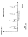
- Figure 1A shows graphically how this works. Specifically, Figure 1A shows a distribution of the threshold voltages of a large population of cells. Because the cells in a flash device are not exactly identical in their characteristics and behavior (due to, for example, small variations in impurity concentrations or defects in the silicon structure), applying the same programming operation to all of the cells does not cause all of the cells to have exactly the same threshold voltage. Instead, the threshold voltage is distributed as shown in Figure 1A . Cells storing a value of "1" typically have a negative threshold voltage, such that most of the cells have a threshold voltage close to the central voltage value of the left peak (labeled 1) of Figure 1A , with fewer cells having threshold voltages lower or higher than the central voltage of the left peak.
- cells storing a value of "0" typically have a positive threshold voltage, such that most of the cells have a threshold voltage close to the central voltage of the right peak (labeled 0) of Figure 1A , with fewer cells having threshold voltages lower or higher than the central voltage of the right peak.
- Multi Level Cells In recent years, a new kind of flash device has appeared on the market, using "Multi Level Cells” (MLC).
- MLC Multi Level Cells
- SBC Single Bit Cell
- MBC Multi-Bit Cell
- MBC flash memories at present are ones with two bits per cell, and therefore examples are given below using such MBC memories. It should however be understood that the present invention is equally applicable to flash memory devices that support more than two bits per cell.
- a single MBC cell storing two bits of information is in one of four different states.
- the cell's "state" is represented by the cell's threshold voltage
- an MBC cell supports four different valid ranges for the cell's threshold voltage.
- Figure 1B shows the threshold voltage distribution for a typical MBC cell of two bits per cell. As expected, Figure 1B has four peaks, each peak corresponding to one state. As for the SBC, each state is actually a voltage range and not a single voltage. When reading the cell's contents, the cell's threshold voltage must be correctly identified in a definite voltage range.
- US Patent No. 5,434,825 to Harari that is included by reference for all purposes as if fully set forth herein.
- a cell designed for MBC operation e . g . in four states is typically operable as an SBC cell with two states.
- Conley et al. in US Patent No. 6,426,893 incorporated by reference for all purposes as if fully set forth herein disclosed the use of both MBC and SBC modes within the same device, and selecting certain parts of the device to operate with highest density in MBC mode, while other parts are used in SBC mode to provide better performance.
- MBC devices provide a significant cost advantage.
- An MBC device with two bits per cell requires about half the area of a silicon wafer than an SBC of similar capacity.
- MBC flash there are drawbacks to using MBC flash. Average read and write times of MBC memories are longer than of SBC memories, resulting in worse performance.
- the reliability of MBC is lower than SBC.
- the differences between the threshold voltage ranges in MBC are much smaller than in SBC.
- a disturbance in the threshold voltage e . g . leakage of stored charge causing a threshold voltage drift or interference from operating neighboring cells
- the end result is a lower performance specification of MBC cells in terms of data retention time or the endurance of the device to many write/erase cycles.
- Flash memory devices are typically divided into NOR devices and NAND devices, the names being derived from the way the individual memory cells are interconnected within the cells array.
- NOR devices are random access - a host computer accessing a NOR flash device can provide the device any address on its address pins and immediately retrieve data stored in that address on the device's data pins. This is much like SRAM or EPROM memories operate.
- NAND devices are not random access but serial access. It is not possible to access any random address in the way described above for NOR - instead the host has to write into the device a sequence of bytes which identifies both the type of the requested command (e.g. read, write, erase, etc.) and the address to be used for that command.
- the address identifies a page (the smallest chunk of flash memory that can we written in a single operation) or a block (the smallest chunk of flash memory that can be erased in a single operation), and not a single byte or word. It is true that the read and write command sequences contain addresses of single bytes or words, but in reality the NAND flash device always reads from the memory cells and writes to the memory cells complete pages. After a page of data is read from the array into a buffer inside the device, the host can access the data bytes or words one by one by serially clocking them out using a strobe signal.
- NAND devices Because of the non-random access of NAND devices, they cannot be used for running code directly from the flash memory. This is contrary to NOR devices which support direct code execution (typically called “eXecution In Place” or “XIP"). Therefore NOR devices are the ones typically used for code storage.
- NOR devices have advantages that make them very useful for data storage. NAND devices are cheaper than NOR devices of the same bit capacity, or equivalently - NAND devices provide many more bits of storage than NOR devices for the same cost. Also, the write and erase performance of NAND devices is much faster than of NOR devices. These advantages make the NAND ⁇ flash memory technology the technology of choice for storing data.
- a typical SBC NAND device is Toshiba TC58NVG1S3B that provides 2Gbit of storage.
- a typical MBC NAND device is Toshiba TC58NVG2D4B that provides 4Gbit of storage.
- the data sheets of both devices are incorporated by reference for all purposes as if fully set forth herein.
- those two NAND devices have a similar interface. These NAND devices use the same electrical signals for coordinating commands and data transfer between the NAND flash device and a host device. Those signals include data lines and a few control signals - ALE (Address Latch Enable), CLE (Command Latch Enable), WE ⁇ (Write Enable), and more.
- ALE Address Latch Enable
- CLE Common Latch Enable
- WE ⁇ Write Enable
- SBC and MBC devices are not fully identical in their behavior - the time it takes to write an MBC page is much longer than time it takes to write an SBC page.
- This type of interface protocol is known in the art as "NAND interface”.
- NAND interface protocol has not, to date, been formally standardized by a standardization body, the manufacturers of NAND flash devices all follow the same protocol for supporting the basic subset of NAND flash functionality. This is done so that customers using NAND devices within their electronic products could use NAND devices from any manufacturer without having to tailor their hardware or software for operating with the devices of a specific vendor. It is noted that even NAND vendors that provide extra functionality beyond this basic subset of functionality ensure that the basic functionality is provided in order to provide compatibility with the protocol used by the other vendors, at least to some extent.
- NAND Interface protocol (or “NAND interface” in short) means an interface protocol between an initiating device and a responding device that in general follows the protocol between a host device and a NAND flash device for the basic read, write and erase operations, even if it is not fully compatible with all timing parameters, not fully compatible with respect to other commands supported by NAND devices, or contains additional commands not supported by NAND devices.
- NAND interface refers to any interface protocol that uses sequences of transferred bytes equivalent in functionality to the sequences of bytes used when interfacing with the Toshiba TC58NVG1S3B NAND device for reading (opcode 00H), writing (opcode 80H) and erasing (opcode 60H), and also uses control signals equivalent in functionality to the CLE, ALE, CE, WE and RE signals of the above NAND device.
- NAND interface protocol is not symmetric. Thus, it is always the host device which initiates the interaction over a NAND interface, and never the flash device.
- a given device e.g. a controller, flash device, host device, etc.
- a given device is said to comprise, include or have a "NAND interface” if the given device includes elements (e.g. hardware, software, firmware or any combination thereof) necessary for supporting the NAND interface protocol (e.g. for interacting with another device using a NAND interface protocol).
- elements e.g. hardware, software, firmware or any combination thereof
- An interface (e.g. a NAND interface or ,an interface associated with another protocol) of a given device may be a "host-side interface” (e.g. the given device is adapted to interact with a host device using the host-side interface) or the interface of the given device may be a "flash memory device-side interface” (e.g. the given device is adapted to interact with a flash memory device using the flash memory device-side interface).
- a host-side interface e.g. the given device is adapted to interact with a host device using the host-side interface
- flash memory device-side interface e.g. the given device is adapted to interact with a flash memory device using the flash memory device-side interface
- host-side interface and “flash device-side interface”
- host-type interface and “flash-type interface” which are terminology used herein to differentiate between the two sides of a NAND interface protocol, as this protocol is not symmetric.
- host-type interface if the device includes the necessary hardware and/or software for implementing the host side of the NAND interface protocol (i.e. for presenting a NAND host, and initiating the NAND protocol interaction).
- flash-type interface if the device includes the necessary hardware and/or software for implementing the flash side of the NAND protocol (i.e. for presenting a NAND flash device).
- host-type interfaces i.e. those which play the role of the host
- flash device-side interfaces i.e. they interact with flash devices or with hardware emulating a flash device
- hosts-side interfaces i.e. they interact with host devices or with hardware emulating a host device
- host device or “host” in short
- a host device may be a personal computer, a PDA, a cellular phone, a game console, etc.
- NAND devices are relatively difficult to interface and work with.
- One reason for that is the relatively complex (compared to NOR devices) protocol for accessing them, as described above.
- Another difficulty is the existence of errors in the data read from NAND devices, In contrast, NOR devices that can be assumed to always return correct data.
- EDC Error Detection Codes
- ECC Error Correction Codes
- N-bit ECC refers to an ECC scheme capable of correcting N bit errors in 512 bytes of data, regardless if the 512 bytes are the size of one page, less than one page, or more than one page.
- NAND controller for controlling the use of a NAND device in an electronic system. It is true that it is possible to operate and use a NAND device directly by a host device with no intervening NAND controller, and there are systems that actually operate like this.
- this architecture suffers from many disadvantages.
- the host has to individually manipulate each one of the NAND device's control signals (e.g. CLE or ALE), which is cumbersome and time-consuming for the host.
- the support of EDC and ECC puts a severe burden on the host - parity bits have to be calculated for each page written, and error detection calculations (and sometimes also error correction calculations) must be performed by the host. All this makes such "no controller" architecture relatively slow and inefficient.
- Using a NAND controller significantly simplifies the host's tasks when using the NAND device.
- the processor interacts with the controller using a protocol that is much more convenient to use - a request for writing a page may be sent as a single command code followed by address and data, instead of having to bother with the complex sequencing of control lines and NAND command codes.
- the controller then converts the host-controller protocol into the equivalent NAND protocol sequences, while the host is free to do other tasks (or just to wait for the NAND operation to complete, if so desired).
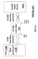
- FIG. 2 A first approach is shown in Figure 2 .
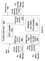
- the NAND controller 114 is physically located within the host processor 112A of the host device 110A. If the host processor 112A is implemented as a single die, then the controller 114 is incorporated on the same die. This is for example the case in some of the OMAP processors manufactured and sold by Texas Instruments.
- the host processor typically interacts with the NAND controller using some proprietary protocol, as the interaction is internal to the host processor and there is no benefit in using a standard protocol.
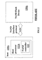
- FIG. 3A-3B A second prior art approach is shown in Figures 3A-3B .
- the NAND controller 116 is a separate physical element, residing between the host processor 112B of the host 110B and the NAND device 120A.
- UFDs portable USB Flash Drives
- M-Systems Flash Disk Pioneers where there is a NAND controller 116 packaged inside the UFD and interacting using a device side NAND interface 124 with the NAND device 120A on one side and with the host processor 112B on the other side (using a host side USB interface 122 which uses the USB protocol).
- the host processor typically interacts with the NAND controller using a standard protocol such as USB or ATA, as the interaction is external to the processor and it is more convenient to use standard protocols that are already supported by the processor for other purposes.
- NAND interface 124 is a "flash memory device side NAND interface” (i.e. adapted to interact with NAND flash device 120A) but at the same time NAND interface 124 is also a host-type NAND interface (i.e. adapted to initiate the NAND protocol interaction).
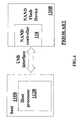
- FIG. 4 A third prior art approach is shown in Figure 4 .
- the NAND controller 118 is physically located within the NAND device 120B.
- the flash device and the controller may even be implemented on the same die. This is for example the case in some of the MDOC storages devices manufactured and sold by M-Systems Flash Disk Pioneers and in the OneNAND devices manufactured and sold by Samsung Electronics.
- the host processor 112B typically interacts with the NAND controller using either a standard protocol such as USB or a semi-standard protocol as is the case in the MDOC and OneNAND examples mentioned above.
- a host processor that does not have built-in NAND support and requires an external controller for that purpose typically does not have a NAND interface and cannot directly connect to a device exporting a NAND interface and therefore has no use of a controller with host-side NAND interface.
- a host processor that has built-in NAND support typically also includes a built-in NAND controller and can connect directly to a NAND device, and therefore has no need for an external NAND controller.
- the prior art described above leaves one problem unsolved. Assume that there is a host processor incorporating a built-in NAND controller and a NAND interface as in Figure 2 .
- the built-in controller is designed to work with NAND devices of a certain level of reliability. This is so because a NAND controller provides a certain level of error detection and correction, and therefore cannot support NAND devices with lower reliability.
- a NAND controller having a 1-bit ECC can work with SBC NAND devices that are specified by their manufacturers to require only this level of error correction.
- Such controller cannot work with two-bit-per-cell MBC NAND devices because they require 4-bit ECC, and therefore some data might not be read correctly into the processor.
- a NAND controller providing 4-bit ECC can work with current two-bit-per-cell MBC NAND, but will not work with next generation MBC NAND devices that will most probably require a higher level of ECC capability.
- the controller 114 supports only 1-bit ECC. Then this processor might not be able to use MBC NAND even though this is highly desirable because of the MBC NAND lower cost. If the MBC NAND is connected to the NAND interface of the built-in controller of the processor, which might be the only way to connect it to the processor, then the MBC NAND generates too many errors for the limited-capability ECC of the built-in controller to correct.
- the built-in controller supports 4-bit ECC, it can use both SLC and two-bit-per-cell MBC NAND. But when NAND devices with lower reliability appear in the market, the processor is not able to benefit from their lower price because its built-in controller is not able to provide the required level of error correction.
- the presently disclosed controller includes (a) electronic circuitry fabricated on a controller die, the controller die being distinct from the flash die, (b) a first interface (for example, a host-type interface) for interfacing between the electronic circuitry and the flash memory device (e.g. the NAND flash memory device), and (c) a second interface (for example, a flash-type interface) for interfacing between the controller and the host device, wherein the second interface is a NAND interface.
- a first interface for example, a host-type interface
- the flash memory device e.g. the NAND flash memory device
- a second interface for example, a flash-type interface
- the first interface is an inter-die interface.
- the first interface is a NAND interface.
- the presently disclosed controller further includes (d) an error correction module for providing error correction for data received through one of the first and second interface.
- the presently disclosed controller further includes (d) at least one additional host-side interface for interfacing with the host device.
- a data storage system including (a) a flash memory device fabricated on a flash die, and (b) the presently disclosed NAND controller, where the controller is operative to communicate with the flash memory device through the first interface.
- the presently disclosed system further includes (c) a common packaging, wherein the flash memory device and the controller are both provided within the common packaging.
- the presently disclosed system further includes (c) separate respective packagings, wherein each of the flash memory device and the controller is provided within a respective packaging.
- the presently disclosed system further includes (c) a printed circuit board on which the flash memory device and the controller are mounted, wherein the flash die is directly mounted on the printed circuit board without a package.
- the presently disclosed system further includes (c) a printed circuit board on which the flash memory device and the controller are mounted, wherein the controller die is directly mounted on the printed circuit board without a package.
- a data storage system including (a) a host device, (b) a flash memory device fabricated on a flash die, and (c) the presently disclosed NAND controller operative to communicate with both the flash memory device through the first interface and with the host device through the second interface.
- a method of writing data from a host device including the steps of: (a) providing a flash memory device fabricated on a flash die and a controller fabricated on a controller die, the flash die being distinct from the controller die, (b) issuing a write command from the host device to the controller according to a NAND interface protocol, and (c) issuing a write command from the controller to the flash memory device according to a NAND interface protocol.
- the presently disclosed method further includes the step of (d) calculating parity bits by the controller.
- a method of reading data to a host device including the steps of: (a) providing a flash memory device fabricated on a flash die and a controller fabricated on a controller die, the flash die being distinct from the controller die, (b) issuing a read command from the host device to the controller according to a NAND interface protocol, and (c) issuing a read command from the controller to the flash memory device according to a NAND interface protocol.
- the presently disclosed method further includes the steps of (d) retrieving the data from the flash memory device to the controller, (e) retrieving parity bits associated with the retrieved data from the flash memory device to the controller, (f) correcting the retrieved data according to the retrieved parity bits, thereby generating corrected data, and (g) retrieving the corrected data from the controller to the host device.
- a method of creating a data storage system including the steps of (a) providing a flash memory device fabricated on a flash die, (b) providing the presently disclosed NAND controller, and (c) deploying the flash controller to the flash memory device such that the flash controller is operative to communicate with the flash memory device through the first interface.
- the presently disclosed method further includes the step of (d) packaging the flash controller and the flash memory device within a single package.
- the flash memory device and the flash controller reside within separate respective packages, and the deploying includes engaging the respective packages to each other.
- the presently disclosed method further includes the step of (d) mounting the flash memory device and the controller onto a printed circuit board, wherein the mounting includes directly mounting the flash memory die onto the printed circuit board without a package.
- the presently disclosed method further includes the step of (d) mounting the flash memory device and the controller onto a printed circuit board, wherein the mounting includes directly mounting the controller die onto the printed circuit board without a package.
- the presently disclosed method further includes the step of (d) deploying the data storage system to a host device such that the flash controller is operative to communicate with the host device through the second interface.
- the present inventor is disclosing for the first time a new type of NAND controller, characterized by the fact that the interface it exports to the host side is a NAND interface.
- this presently disclosed controller has NAND interfaces on both sides - on the flash memory device side, where the controller plays the role of a host towards the NAND device, and on the host device side, where the controller plays the role of a NAND device towards the host.
- a “NAND flash memory device” is defined as electronic circuitry including a plurality of NAND flash memory cells and any necessary control circuitry (e.g. circuitry for providing a flash-type interface) for storing data within the NAND flash memory cells. It is noted that the “NAND flash memory device” does not necessarily have its own dedicated housing, and may reside with another “device” such as a controller within a single housing. In some embodiments, the “NAND flash memory device” is directly mounted onto a printed circuit board without any packing.
- the controller includes an error correction capability that is sufficient for correcting the many errors of a lower-reliability NAND device. Because these errors are corrected by the controller, the controller can present to the host a flash device having no errors at all, or having a smaller number of errors - small enough for the error correction capability of the host's built-in NAND controller to handle.
- Controller 130 includes a flash memory device-side NAND interface 142 for interfacing to a NAND flash device. Furthermore, it is noted that flash memory device-side NAND interface 142 is also a host-type NAND interface (i.e. adapted to initiate the interaction over the NAND interface, and to present a host device to a NAND flash device).
- flash memory device-side NAND interface 142 is also a host-type NAND interface (i.e. adapted to initiate the interaction over the NAND interface, and to present a host device to a NAND flash device).
- the controller 130 also includes a host side NAND interface 144 for interfacing to a host that supports a NAND interface protocol.
- This host side NAND interface is also a flash memory-type NAND interface (e.g. the controller 130 is adapted to present to the host a NAND flash memory storage device).
- the controller may optionally include one or more additional host-side interfaces 146, for interfacing the controller to hosts using non-NAND interfaces, such as USB or MMC interfaces.
- the controller further includes an ECC module 132 for detecting and correcting all or some of the errors in the data retrieved from the NAND device through device-side interface 142.
- the ECC module 132 may include hardware, software, firmware or any combination thereof.
- the ECC module 132 may correct all errors, in which case the NAND controller 130 exports to the host an error-free NAND device. Alternatively, the ECC module 132 may correct only some of the errors found in the data retrieved from the NAND device through the flash memory device-side NAND interface 142.
- the NAND device may have a reliability that requires 4-bit ECC, and the ECC module 142 corrects enough of the errors to increase the data reliability up to the level that enables a 1-bit ECC module in the host's built-in NAND controller to handle the data.
- NAND controller 130 may optionally also include one or more modules 134 (e.g. including hardware, software, firmware or any combination thereof) for providing other functionality, such as encryption functionality or address mapping that maps logical flash addresses received from the host into physical flash addresses sent to the flash device.
- modules 134 e.g. including hardware, software, firmware or any combination thereof
- Figure 5B shows a schematic block diagram of an exemplary system including the external NAND controller 130 (e.g. a controller separate from the host device) described in Figure 5A .
- the external NAND controller 130 e.g. a controller separate from the host device
- the external NAND controller 130 interfaces with NAND flash device 120A.
- host side NAND interface 144 the NAND controller 130 interfaces with host device 110A.
- NAND interface protocol is not symmetrical - there is an initiator side that initiates the transactions ("host-type” according to the previously defined terminology) and there is a responding side that only responds to the initiating signals ("flash-type” according to the previously defined terminology).
- external NAND controller 130 acts as the host-type part of the NAND interface protocol and the NAND device 130 acts as the flash-type part of the NAND interface protocol.
- host side interface 144 external controller 130 acts as the flash-type part of the NAND interface protocol and host 110A acts as the host-type part of the NAND interface protocol.
- Figure 6A shows an exemplary die configuration of the exemplary system described in Figure 5A .
- the NAND controller 130 includes electronic circuitry 135 fabricated on a controller die 131 while the NAND flash device 120A includes electronic circuitry 137 fabricated on a flash die 133.
- the controller die 131 and the flash die 133 are distinct dies.
- elements within the NAND controller 130 as described in Figure 5A i.e. the ECC module 132, the flash-type NAND interface 144, the host-type NAND interfaces
- the controller electronic circuitry 135 residing on the controller die.
- the interface 142 between the controller electronic circuitry 135 and the flash electronic circuitry 137 is an "inter-die” interface.
- an "inter-die interface” e.g. an inter-die NAND interface
- the inter-die interface includes the necessary physical elements (pads, output and input drivers, etc) for interfacing between the two distinct units of electronic circuitry residing on separate dies.
- an inter-die interface may interface between electronic circuitry fabricated on two distinct dies that are packaged in a common package. This example is illustrated in Figure 6B , wherein both the NAND controller 130 and the NAND flash device 120A reside within a common multi-chip package 139.
- the inter-die interface may interface between electronic circuitry fabricated on two distinct dies packaged in distinct packages (for example, where each die is packaged in its own package).
- This example is illustrated in Figure 6C , wherein the NAND controller 130 and the NAND flash device 120A reside in separate respective packages.
- the NAND controller 130 resides within controller package 141, while the NAND flash device 120A resides within flash package 143.
- interface 142 is an "inter-package interface.”
- the inter-die interface may interface between electronic circuitry fabricated on two distinct dies, where one or both of these dies has no package at all.
- memory dies are provided (e.g. mounted, for example, directly mounted) on boards with no packaging at all.
- memory dies are often mounted on boards with no packaging at all.
- a die which is "directly mounted" onto a printed circuit board is mounted on the printed circuit board without being packaged first.
- Figure 7 shows a flow chart describing a method wherein a host 110A (e.g. a host including a NAND controller 114 within the device) writes data (e.g. a page of data) to a NAND storage device 120A via an external NAND controller 130.
- the host 110A issues 410 a write command to the external controller 130 (e.g. a write command issued using the NAND interface protocol, including command bytes, address bytes and data bytes).
- the host 110A is not necessarily aware of the fact it is issuing the command to a controller 130, and may assume it is interfacing with a standard NAND flash storage device of the type it is capable of handling.
- the NAND controller 130 receives the write command issued by the host (e.g. via the host-side NAND interface 144 ). After receiving the write command, the controller calculates ECC parity bits 420 (e.g. using ECC module 132 ) corresponding to the data bytes, and issues 430 a write command to the NAND device (e.g. via the flash memory device side interface 142 ). Again, the command is issued according to the NAND interface protocol, including command bytes, address bytes and data bytes that contain both the host's data bytes and the corresponding ECC parity bits.
- the NAND flash storage device is not necessarily aware that it received the command indirectly via the NAND controller 130 and not directly from the host device 110A. In step 440 the NAND flash storage device 120A stores the data bytes it received into the non-volatile memory cells, thus fulfilling the host's 110A request.
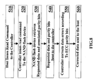
- Figure 8 shows a flowchart describing a method wherein a host 110A (e.g. a host including a NAND controller 114 within the device) reads data (e.g. a page of data) from a NAND storage device 120A via an external NAND controller 130.
- the host 110A issues 410 a read command to the external controller 130 (e.g. a read command issued using the NAND interface protocol, including command bytes and address bytes).
- the host 110A is not necessarily aware of the fact it is issuing the command to an external controller 130, and may assume it is interfacing with a standard NAND device of the type it is capable of handling.
- the external NAND controller 130 receives the read command issued by the host (e.g. via the host-side NAND interface 144). After receiving the read command, the external controller 130 issues 520 a read command (e.g. via the device-side NAND interface 142) to the NAND device 120A. Again, the command is issued according to the NAND interface protocol, including command bytes and address bytes.
- the NAND flash storage device 120A retrieves the requested data from the non-volatile cells array, where the host data is accompanied by the ECC parity bits calculated when the data had been stored.
- step 540 the data bytes and the accompanying parity bits are sent to the external NAND controller.
- This sending is done according to the NAND interface protocol by a series of read strobes generated by the controller, each sequentially reading into the controller one byte or one word (depending on whether the NAND interface used is 8 bits wide or 16 bits wide).
- the external NAND controller 130 uses the parity bits for correcting errors in the data bytes (e.g. with the ECC module 132).
- the corrected data bytes are sent to the host via the host side NAND interface 144.
- the sending is again done according to the NAND interface protocol by a series of read strobes generated by the host.
- the host 110A now has the same data bytes it originally stored into the flash memory.
- this invention allows one to benefit from the cost advantage of new NAND devices, while using a host processor incorporating a built-in NAND controller designed to support a previous generation of NAND devices.
- each of the verbs, "comprise” “include” and “have”, and conjugates thereof, are used to indicate that the object or objects of the verb are not necessarily a complete listing of members, components, elements or parts of the subject or subjects of the verb.
Landscapes
- Engineering & Computer Science (AREA)
- Theoretical Computer Science (AREA)
- Physics & Mathematics (AREA)
- General Engineering & Computer Science (AREA)
- General Physics & Mathematics (AREA)
- Quality & Reliability (AREA)
- Microelectronics & Electronic Packaging (AREA)
- Techniques For Improving Reliability Of Storages (AREA)
- Read Only Memory (AREA)
Abstract

Description
- The present invention relates to NAND flash memory controllers that export to the host computer the same type of interface that is exported by a standard NAND flash memory device.
- Flash memory devices have been known for many years. Typically, each memory cell within a flash memory device stores one bit of information. The traditional way to store a bit in a flash memory cell has been by supporting two states of the memory cell. One state represents a logical "0" and the other state represents a logical "1".
- In a flash memory cell, the two states are implemented by having a floating gate situated above the cell's channel (the area connecting the source and drain elements of the cell's transistor), and having two valid states for the amount of charge stored within the floating gate. Typically, one state is with zero charge in the floating gate and is the unwritten state of the cell after being erased (commonly defined to represent the "1" state) and the other state is with some amount of negative charge in the floating gate (commonly defined to represent the "0" state). Having negative charge in the gate causes the threshold voltage of the cell's transistor (i.e. the voltage that has to be applied to the transistor's control gate in order to cause the transistor to conduct) to increase. It is possible to read the stored bit by checking the threshold voltage of the cell. If the threshold voltage is in the higher state then the bit value is "0" and if the threshold voltage is in the lower state then the bit value is "1". Actually there is no need to accurately read the cell's threshold voltage. All that is needed is to correctly identify in which of the two states the cell is currently located. For this purpose it is sufficient to compare the threshold voltage of the cell to a reference voltage that is between the two states, and to determine if the cell's threshold voltage is below or above the reference value.
-
Figure 1A (prior art) shows graphically how this works. Specifically,Figure 1A shows a distribution of the threshold voltages of a large population of cells. Because the cells in a flash device are not exactly identical in their characteristics and behavior (due to, for example, small variations in impurity concentrations or defects in the silicon structure), applying the same programming operation to all of the cells does not cause all of the cells to have exactly the same threshold voltage. Instead, the threshold voltage is distributed as shown inFigure 1A . Cells storing a value of "1" typically have a negative threshold voltage, such that most of the cells have a threshold voltage close to the central voltage value of the left peak (labeled 1) ofFigure 1A , with fewer cells having threshold voltages lower or higher than the central voltage of the left peak. Similarly, cells storing a value of "0" typically have a positive threshold voltage, such that most of the cells have a threshold voltage close to the central voltage of the right peak (labeled 0) ofFigure 1A , with fewer cells having threshold voltages lower or higher than the central voltage of the right peak. - In recent years, a new kind of flash device has appeared on the market, using "Multi Level Cells" (MLC). The term "Multi-Level Cell" is misleading because flash memory with a single bit per cell uses multiple i.e. two levels, as described above. Therefore, the term "Single Bit Cell" (SBC) is used hereinafter to refer to a memory cell of two levels and the term "Multi-Bit Cell" (MBC) is used hereinafter to refer to a memory cell of more than two levels, i.e. more than one bit per cell. The most common MBC flash memories at present are ones with two bits per cell, and therefore examples are given below using such MBC memories. It should however be understood that the present invention is equally applicable to flash memory devices that support more than two bits per cell. A single MBC cell storing two bits of information is in one of four different states. As the cell's "state" is represented by the cell's threshold voltage, an MBC cell supports four different valid ranges for the cell's threshold voltage.
Figure 1B (prior art) shows the threshold voltage distribution for a typical MBC cell of two bits per cell. As expected,Figure 1B has four peaks, each peak corresponding to one state. As for the SBC, each state is actually a voltage range and not a single voltage. When reading the cell's contents, the cell's threshold voltage must be correctly identified in a definite voltage range. For a prior art example of an MBC flash device seeUS Patent No. 5,434,825 to Harari that is included by reference for all purposes as if fully set forth herein. - A cell designed for MBC operation e.g. in four states is typically operable as an SBC cell with two states. For example,
Conley et al. in US Patent No. 6,426,893 incorporated by reference for all purposes as if fully set forth herein, disclosed the use of both MBC and SBC modes within the same device, and selecting certain parts of the device to operate with highest density in MBC mode, while other parts are used in SBC mode to provide better performance. - MBC devices provide a significant cost advantage. An MBC device with two bits per cell requires about half the area of a silicon wafer than an SBC of similar capacity. However, there are drawbacks to using MBC flash. Average read and write times of MBC memories are longer than of SBC memories, resulting in worse performance. Also, the reliability of MBC is lower than SBC. The differences between the threshold voltage ranges in MBC are much smaller than in SBC. Thus, a disturbance in the threshold voltage (e.g. leakage of stored charge causing a threshold voltage drift or interference from operating neighboring cells) that are insignificant in SBC because of the large gap between the two states, may cause an MBC cell to move from one state to another, resulting in an erroneous bit. The end result is a lower performance specification of MBC cells in terms of data retention time or the endurance of the device to many write/erase cycles.
- Flash memory devices are typically divided into NOR devices and NAND devices, the names being derived from the way the individual memory cells are interconnected within the cells array. NOR devices are random access - a host computer accessing a NOR flash device can provide the device any address on its address pins and immediately retrieve data stored in that address on the device's data pins. This is much like SRAM or EPROM memories operate. NAND devices, on the other hand, are not random access but serial access. It is not possible to access any random address in the way described above for NOR - instead the host has to write into the device a sequence of bytes which identifies both the type of the requested command (e.g. read, write, erase, etc.) and the address to be used for that command. The address identifies a page (the smallest chunk of flash memory that can we written in a single operation) or a block (the smallest chunk of flash memory that can be erased in a single operation), and not a single byte or word. It is true that the read and write command sequences contain addresses of single bytes or words, but in reality the NAND flash device always reads from the memory cells and writes to the memory cells complete pages. After a page of data is read from the array into a buffer inside the device, the host can access the data bytes or words one by one by serially clocking them out using a strobe signal.
- Because of the non-random access of NAND devices, they cannot be used for running code directly from the flash memory. This is contrary to NOR devices which support direct code execution (typically called "eXecution In Place" or "XIP"). Therefore NOR devices are the ones typically used for code storage. However, NAND devices have advantages that make them very useful for data storage. NAND devices are cheaper than NOR devices of the same bit capacity, or equivalently - NAND devices provide many more bits of storage than NOR devices for the same cost. Also, the write and erase performance of NAND devices is much faster than of NOR devices. These advantages make the NAND·flash memory technology the technology of choice for storing data.
- A typical SBC NAND device is Toshiba TC58NVG1S3B that provides 2Gbit of storage. A typical MBC NAND device is Toshiba TC58NVG2D4B that provides 4Gbit of storage. The data sheets of both devices are incorporated by reference for all purposes as if fully set forth herein.
- As can be seen from the aforementioned data sheets, those two NAND devices have a similar interface. These NAND devices use the same electrical signals for coordinating commands and data transfer between the NAND flash device and a host device. Those signals include data lines and a few control signals - ALE (Address Latch Enable), CLE (Command Latch Enable), WE\ (Write Enable), and more. The SBC and MBC devices are not fully identical in their behavior - the time it takes to write an MBC page is much longer than time it takes to write an SBC page. However, the electrical signals used in both devices and their functionalities are the same. This type of interface protocol is known in the art as "NAND interface". Even though the "NAND interface protocol" has not, to date, been formally standardized by a standardization body, the manufacturers of NAND flash devices all follow the same protocol for supporting the basic subset of NAND flash functionality. This is done so that customers using NAND devices within their electronic products could use NAND devices from any manufacturer without having to tailor their hardware or software for operating with the devices of a specific vendor. It is noted that even NAND vendors that provide extra functionality beyond this basic subset of functionality ensure that the basic functionality is provided in order to provide compatibility with the protocol used by the other vendors, at least to some extent.
- In this application the term "NAND Interface protocol" (or "NAND interface" in short) means an interface protocol between an initiating device and a responding device that in general follows the protocol between a host device and a NAND flash device for the basic read, write and erase operations, even if it is not fully compatible with all timing parameters, not fully compatible with respect to other commands supported by NAND devices, or contains additional commands not supported by NAND devices. In other words, the term "NAND interface" refers to any interface protocol that uses sequences of transferred bytes equivalent in functionality to the sequences of bytes used when interfacing with the Toshiba TC58NVG1S3B NAND device for reading (opcode 00H), writing (opcode 80H) and erasing (opcode 60H), and also uses control signals equivalent in functionality to the CLE, ALE, CE, WE and RE signals of the above NAND device.
- It is noted that the "NAND interface protocol" is not symmetric. Thus, it is always the host device which initiates the interaction over a NAND interface, and never the flash device.
- A given device (e.g. a controller, flash device, host device, etc.) is said to comprise, include or have a "NAND interface" if the given device includes elements (e.g. hardware, software, firmware or any combination thereof) necessary for supporting the NAND interface protocol (e.g. for interacting with another device using a NAND interface protocol).
- An interface (e.g. a NAND interface or ,an interface associated with another protocol) of a given device (e.g. a controller device) may be a "host-side interface" (e.g. the given device is adapted to interact with a host device using the host-side interface) or the interface of the given device may be a "flash memory device-side interface" (e.g. the given device is adapted to interact with a flash memory device using the flash memory device-side interface). The terms "flash memory device-side interface", "flash device-side interface" and "flash-side interface" are used herein interchangeably.
- These terms (i.e. "host-side interface" and "flash device-side interface") should not be confused with the terms "host-type interface" and "flash-type interface" which are terminology used herein to differentiate between the two sides of a NAND interface protocol, as this protocol is not symmetric. Furthermore, because it is always the host that initiates the interaction, we note that a given device is said to have a "host-type interface" if the device includes the necessary hardware and/or software for implementing the host side of the NAND interface protocol (i.e. for presenting a NAND host, and initiating the NAND protocol interaction). Similarly, because the flash device never initiates the interaction, we note that a given device is said to have a "flash-type interface" if the device includes the necessary hardware and/or software for implementing the flash side of the NAND protocol (i.e. for presenting a NAND flash device).
- Typically, "host-type interfaces" (i.e. those which play the role of the host) are "flash device-side interfaces" (i.e. they interact with flash devices or with hardware emulating a flash device) while "flash device-type interfaces" (i.e. those which play the role of the flash device) are typically "hosts-side interfaces" (i.e. they interact with host devices or with hardware emulating a host device). In this application the term "host device" (or "host" in short) means any device that has processing power and is capable of interfacing with a flash memory device. A host device may be a personal computer, a PDA, a cellular phone, a game console, etc.
- Typically, NAND devices are relatively difficult to interface and work with. One reason for that is the relatively complex (compared to NOR devices) protocol for accessing them, as described above. Another difficulty is the existence of errors in the data read from NAND devices, In contrast, NOR devices that can be assumed to always return correct data. This inherent non-reliability of NAND devices requires the use of Error Detection Codes (EDC) and Error Correction Codes (ECC).
- Manufacturers of SBC NAND flash devices typically advise users to apply an Error Correction Code capable of correcting 1 bit error in each page of 512 bytes of data. But data sheets of MBC NAND flash devices typically advise applying an ECC capable of correcting 4 bit errors in each page of 512 bytes of data. For pages of size 2048 bytes such as in the case of the NAND devices mentioned above (known as "large block devices"), the suggestion is to apply error correction per each portion of 512 bytes of the page. In this application the term "N-bit ECC" refers to an ECC scheme capable of correcting N bit errors in 512 bytes of data, regardless if the 512 bytes are the size of one page, less than one page, or more than one page.
- Because of those complexities of NAND devices, it is the common practice to use a "NAND controller" for controlling the use of a NAND device in an electronic system. It is true that it is possible to operate and use a NAND device directly by a host device with no intervening NAND controller, and there are systems that actually operate like this. However, this architecture suffers from many disadvantages. First, the host has to individually manipulate each one of the NAND device's control signals (e.g. CLE or ALE), which is cumbersome and time-consuming for the host. Second, the support of EDC and ECC puts a severe burden on the host - parity bits have to be calculated for each page written, and error detection calculations (and sometimes also error correction calculations) must be performed by the host. All this makes such "no controller" architecture relatively slow and inefficient.
- Using a NAND controller significantly simplifies the host's tasks when using the NAND device. The processor interacts with the controller using a protocol that is much more convenient to use - a request for writing a page may be sent as a single command code followed by address and data, instead of having to bother with the complex sequencing of control lines and NAND command codes. The controller then converts the host-controller protocol into the equivalent NAND protocol sequences, while the host is free to do other tasks (or just to wait for the NAND operation to complete, if so desired).
- There are several options in the prior art regarding the location where the NAND controller resides within the system. A first approach is shown in
Figure 2 . Here theNAND controller 114 is physically located within thehost processor 112A of thehost device 110A. If thehost processor 112A is implemented as a single die, then thecontroller 114 is incorporated on the same die. This is for example the case in some of the OMAP processors manufactured and sold by Texas Instruments. In a system built using this architecture the host processor typically interacts with the NAND controller using some proprietary protocol, as the interaction is internal to the host processor and there is no benefit in using a standard protocol. - A second prior art approach is shown in
Figures 3A-3B . Here theNAND controller 116 is a separate physical element, residing between thehost processor 112B of thehost 110B and theNAND device 120A. This is for example the case in portable USB Flash Drives (UFDs), such as the DiskOnKey manufactured and sold by M-Systems Flash Disk Pioneers, where there is aNAND controller 116 packaged inside the UFD and interacting using a deviceside NAND interface 124 with theNAND device 120A on one side and with thehost processor 112B on the other side (using a hostside USB interface 122 which uses the USB protocol). In a system built using this architecture the host processor typically interacts with the NAND controller using a standard protocol such as USB or ATA, as the interaction is external to the processor and it is more convenient to use standard protocols that are already supported by the processor for other purposes. - Note that according to the terminology previously defined,
NAND interface 124 is a "flash memory device side NAND interface" (i.e. adapted to interact withNAND flash device 120A) but at the sametime NAND interface 124 is also a host-type NAND interface (i.e. adapted to initiate the NAND protocol interaction). - A third prior art approach is shown in
Figure 4 . Here theNAND controller 118 is physically located within theNAND device 120B. The flash device and the controller may even be implemented on the same die. This is for example the case in some of the MDOC storages devices manufactured and sold by M-Systems Flash Disk Pioneers and in the OneNAND devices manufactured and sold by Samsung Electronics. In a system built using this architecture thehost processor 112B typically interacts with the NAND controller using either a standard protocol such as USB or a semi-standard protocol as is the case in the MDOC and OneNAND examples mentioned above. - We can deduce from the above that a prior art stand-alone NAND controller (that is not integrated with neither the NAND device nor the host processor) will typically have some standard interface on its host side, and a NAND interface on its flash memory device side (for example, see
Figure 3B ). Indeed one can find in the market NAND controllers exporting many interface types - USB, SD (SecureDigital), MMC (MultiMediaCard), and more. However, one cannot currently find a stand-alone NAND controller that exports NAND interface to the host. Indeed, this is reasonable to expect - a host processor that does not have built-in NAND support and requires an external controller for that purpose, typically does not have a NAND interface and cannot directly connect to a device exporting a NAND interface and therefore has no use of a controller with host-side NAND interface. On the other hand, a host processor that has built-in NAND support typically also includes a built-in NAND controller and can connect directly to a NAND device, and therefore has no need for an external NAND controller. - The prior art described above leaves one problem unsolved. Assume that there is a host processor incorporating a built-in NAND controller and a NAND interface as in
Figure 2 . The built-in controller is designed to work with NAND devices of a certain level of reliability. This is so because a NAND controller provides a certain level of error detection and correction, and therefore cannot support NAND devices with lower reliability. For example, a NAND controller having a 1-bit ECC can work with SBC NAND devices that are specified by their manufacturers to require only this level of error correction. Such controller cannot work with two-bit-per-cell MBC NAND devices because they require 4-bit ECC, and therefore some data might not be read correctly into the processor. Similarly, a NAND controller providing 4-bit ECC can work with current two-bit-per-cell MBC NAND, but will not work with next generation MBC NAND devices that will most probably require a higher level of ECC capability. - This is so because future MBC NAND devices are expected to be less reliable than current MBC devices and to require a much stronger ECC capability. The reasons for the reduced reliability and increased error rate are twofold:
- a. The process used for manufacturing NAND devices is continuously being improved to yield smaller memory cells. While a few years ago NAND devices used 0.4 micron process, currently they use 90 nm and 70 nm technology, and this shrinking trend is expected to continue. With shrinking dimensions of the memory cells comes lower reliability, as the small dimensions make the cells more sensitive to physical effects and phenomena that previously were not important.
- b. When MBC cells with more than two bits per cell will become commercially available, they will necessarily be much less reliable than SBC cells and two-bit-per-cell MBC cells. The larger number of states that have to be represented by the cell's threshold voltage imply that the margins between states are smaller and even smaller disturbances and drifts result in incorrect reading of data. This effect could already be witnessed in the comparison between SLC and two-bit-per-cell MBC, where the ECC requirements increased from 1-bit ECC to 4-bit ECC.
- Returning now to the
host processor 112A with the built-inNAND controller 114, suppose thecontroller 114 supports only 1-bit ECC. Then this processor might not be able to use MBC NAND even though this is highly desirable because of the MBC NAND lower cost. If the MBC NAND is connected to the NAND interface of the built-in controller of the processor, which might be the only way to connect it to the processor, then the MBC NAND generates too many errors for the limited-capability ECC of the built-in controller to correct. - Similarly, if the built-in controller supports 4-bit ECC, it can use both SLC and two-bit-per-cell MBC NAND. But when NAND devices with lower reliability appear in the market, the processor is not able to benefit from their lower price because its built-in controller is not able to provide the required level of error correction.
- Therefore we see that the state of the prior art does not provide a good solution to the problem of benefiting from the cost advantage of a new NAND device, while using a host processor incorporating a built-in NAND controller designed to support a previous generation of NAND devices.
- There is an ongoing need for devices and methods that provide compatibility between a host device having an onboard NAND controller and successive generations of NAND flash memory devices.
- The aforementioned needs are satisfied by several aspects of the present invention.
- It is now disclosed for the first time a controller for interfacing between a host device and a flash memory device (e.g. a NAND flash memory device) fabricated on a flash die. The presently disclosed controller includes (a) electronic circuitry fabricated on a controller die, the controller die being distinct from the flash die, (b) a first interface (for example, a host-type interface) for interfacing between the electronic circuitry and the flash memory device (e.g. the NAND flash memory device), and (c) a second interface (for example, a flash-type interface) for interfacing between the controller and the host device, wherein the second interface is a NAND interface.
- According to some embodiments, the first interface is an inter-die interface.
- According to some embodiments, the first interface is a NAND interface.
- According to some embodiments, the presently disclosed controller further includes (d) an error correction module for providing error correction for data received through one of the first and second interface.
- According to some embodiments, the presently disclosed controller further includes (d) at least one additional host-side interface for interfacing with the host device.
- It is now disclosed for the first time a data storage system including (a) a flash memory device fabricated on a flash die, and (b) the presently disclosed NAND controller, where the controller is operative to communicate with the flash memory device through the first interface.
- According to some embodiments, the presently disclosed system further includes (c) a common packaging, wherein the flash memory device and the controller are both provided within the common packaging.
- According to some embodiments, the presently disclosed system further includes (c) separate respective packagings, wherein each of the flash memory device and the controller is provided within a respective packaging.
- According to some embodiments, the presently disclosed system further includes (c) a printed circuit board on which the flash memory device and the controller are mounted, wherein the flash die is directly mounted on the printed circuit board without a package.
- According to some embodiments, the presently disclosed system further includes (c) a printed circuit board on which the flash memory device and the controller are mounted, wherein the controller die is directly mounted on the printed circuit board without a package.
- It is now disclosed for the first time a data storage system including (a) a host device, (b) a flash memory device fabricated on a flash die, and (c) the presently disclosed NAND controller operative to communicate with both the flash memory device through the first interface and with the host device through the second interface.
- It is now disclosed a method of writing data from a host device including the steps of: (a) providing a flash memory device fabricated on a flash die and a controller fabricated on a controller die, the flash die being distinct from the controller die, (b) issuing a write command from the host device to the controller according to a NAND interface protocol, and (c) issuing a write command from the controller to the flash memory device according to a NAND interface protocol.
- According to some embodiments, the presently disclosed method further includes the step of (d) calculating parity bits by the controller.
- It is now disclosed a method of reading data to a host device including the steps of: (a) providing a flash memory device fabricated on a flash die and a controller fabricated on a controller die, the flash die being distinct from the controller die, (b) issuing a read command from the host device to the controller according to a NAND interface protocol, and (c) issuing a read command from the controller to the flash memory device according to a NAND interface protocol.
- According to some embodiments, the presently disclosed method further includes the steps of (d) retrieving the data from the flash memory device to the controller, (e) retrieving parity bits associated with the retrieved data from the flash memory device to the controller, (f) correcting the retrieved data according to the retrieved parity bits, thereby generating corrected data, and (g) retrieving the corrected data from the controller to the host device.
- It is now disclosed for the first time a method of creating a data storage system including the steps of (a) providing a flash memory device fabricated on a flash die, (b) providing the presently disclosed NAND controller, and (c) deploying the flash controller to the flash memory device such that the flash controller is operative to communicate with the flash memory device through the first interface.
- According to some embodiments, the presently disclosed method further includes the step of (d) packaging the flash controller and the flash memory device within a single package.
- According to some embodiments, the flash memory device and the flash controller reside within separate respective packages, and the deploying includes engaging the respective packages to each other.
- According to some embodiments, the presently disclosed method further includes the step of (d) mounting the flash memory device and the controller onto a printed circuit board, wherein the mounting includes directly mounting the flash memory die onto the printed circuit board without a package..
- According to some embodiments, the presently disclosed method further includes the step of (d) mounting the flash memory device and the controller onto a printed circuit board, wherein the mounting includes directly mounting the controller die onto the printed circuit board without a package.
- According to some embodiments, the presently disclosed method further includes the step of (d) deploying the data storage system to a host device such that the flash controller is operative to communicate with the host device through the second interface.
- These and further embodiments will be apparent from the detailed description and examples that follow.
-
-
Figures 1A-1B provide a graphical illustration of distributions of thresholds voltages of a large population of memory cells (prior art). -
Figure 2 provides a block diagram of a prior art system including a host device and a NAND flash device. -
Figure 3A provides a block diagram of a prior art system including a host device, a NAND controller and a NAND flash device. -
Figure 3B provides a block diagram of a prior art NAND controller having a USB interface on the host side and a NAND interface on the flash memory device side. -
Figure 4 provides a block diagram of a prior art system including a host device and a NAND flash device. -
Figure 5A provides a block diagram of a NAND controller having a NAND interface on the host side and a NAND interface on the flash memory device side in accordance with exemplary embodiments of the present invention. -
Figure 5B provides a block diagram of a system including a host device, the NAND controller ofFigure 5A , and a NAND flash device in accordance with exemplary embodiments of the present invention. -
Figure 6A illustrates an exemplary die configuration of the exemplary system described inFigure 5B . -
Figure 6B illustrates an exemplary configuration of the exemplary system described inFigure 5B where the NAND controller and the NAND flash device reside within a single multi-chip package. -
Figure 6C illustrates an exemplary configuration of the exemplary system described inFigure 5B where the NAND controller and the NAND flash device reside within separate respective packages. -
Figure 7 shows a flow chart describing a method wherein a host writes data to a NAND storage device via an external NAND controller. -
Figure 8 shows a flowchart describing a method wherein a host reads data from a NAND storage device 120 via an external NAND controller. - The present invention will now be described in terms of specific, example embodiments. It is to be understood that the invention is not limited to the example embodiments disclosed. It should also be understood that not every feature of the controllers, systems including controllers, and methods of reading and data described is necessary to implement the invention as claimed in any particular one of the appended claims. Various elements and features of devices are described to fully enable the invention. It should also be understood that throughout this disclosure, where a process or method is shown or described, the steps of the method may be performed in any order or simultaneously, unless it is clear from the context that one step depends on another being performed first.
- The present inventor is disclosing for the first time a new type of NAND controller, characterized by the fact that the interface it exports to the host side is a NAND interface. In some embodiments, this presently disclosed controller has NAND interfaces on both sides - on the flash memory device side, where the controller plays the role of a host towards the NAND device, and on the host device side, where the controller plays the role of a NAND device towards the host.
- For the purposes of this disclosure, a "NAND flash memory device" is defined as electronic circuitry including a plurality of NAND flash memory cells and any necessary control circuitry (e.g. circuitry for providing a flash-type interface) for storing data within the NAND flash memory cells. It is noted that the "NAND flash memory device" does not necessarily have its own dedicated housing, and may reside with another "device" such as a controller within a single housing. In some embodiments, the "NAND flash memory device" is directly mounted onto a printed circuit board without any packing.
- Furthermore, in some embodiments, the controller includes an error correction capability that is sufficient for correcting the many errors of a lower-reliability NAND device. Because these errors are corrected by the controller, the controller can present to the host a flash device having no errors at all, or having a smaller number of errors - small enough for the error correction capability of the host's built-in NAND controller to handle.
- Attention is now called to
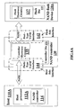
Figure 5A , which provides a schematic block diagram of a controller in accordance with some embodiments of the present invention.Controller 130 includes a flash memory device-side NAND interface 142 for interfacing to a NAND flash device. Furthermore, it is noted that flash memory device-side NAND interface 142 is also a host-type NAND interface (i.e. adapted to initiate the interaction over the NAND interface, and to present a host device to a NAND flash device). - The
controller 130 also includes a hostside NAND interface 144 for interfacing to a host that supports a NAND interface protocol. This host side NAND interface is also a flash memory-type NAND interface (e.g. thecontroller 130 is adapted to present to the host a NAND flash memory storage device). The controller may optionally include one or more additional host-side interfaces 146, for interfacing the controller to hosts using non-NAND interfaces, such as USB or MMC interfaces. - As shown in
Figure 5A , the controller further includes anECC module 132 for detecting and correcting all or some of the errors in the data retrieved from the NAND device through device-side interface 142. TheECC module 132 may include hardware, software, firmware or any combination thereof. TheECC module 132 may correct all errors, in which case theNAND controller 130 exports to the host an error-free NAND device. Alternatively, theECC module 132 may correct only some of the errors found in the data retrieved from the NAND device through the flash memory device-side NAND interface 142. - In one example, the NAND device may have a reliability that requires 4-bit ECC, and the
ECC module 142 corrects enough of the errors to increase the data reliability up to the level that enables a 1-bit ECC module in the host's built-in NAND controller to handle the data. - It is noted that
NAND controller 130 may optionally also include one or more modules 134 (e.g. including hardware, software, firmware or any combination thereof) for providing other functionality, such as encryption functionality or address mapping that maps logical flash addresses received from the host into physical flash addresses sent to the flash device. - Attention is now called to
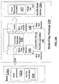
Figure 5B which shows a schematic block diagram of an exemplary system including the external NAND controller 130 (e.g. a controller separate from the host device) described inFigure 5A . Through deviceside NAND interface 142 theexternal NAND controller 130 interfaces withNAND flash device 120A. Through hostside NAND interface 144, theNAND controller 130 interfaces withhost device 110A. - One should note that the way
external controller 130 interfaces through the twoNAND interfaces - Using device
side NAND interface 142,external NAND controller 130 acts as the host-type part of the NAND interface protocol and theNAND device 130 acts as the flash-type part of the NAND interface protocol. Usinghost side interface 144,external controller 130 acts as the flash-type part of the NAND interface protocol and host 110A acts as the host-type part of the NAND interface protocol. - Attention is now called to
Figure 6A which shows an exemplary die configuration of the exemplary system described inFigure 5A . Thus, it is noted that theNAND controller 130 includeselectronic circuitry 135 fabricated on a controller die 131 while theNAND flash device 120A includeselectronic circuitry 137 fabricated on aflash die 133. The controller die 131 and the flash die 133 are distinct dies. - It is noted that elements within the
NAND controller 130 as described inFigure 5A (i.e. theECC module 132, the flash-type NAND interface 144, the host-type NAND interfaces) are implemented at least in part by the controllerelectronic circuitry 135 residing on the controller die. - The
interface 142 between the controllerelectronic circuitry 135 and the flashelectronic circuitry 137 is an "inter-die" interface. As used herein, an "inter-die interface" (e.g. an inter-die NAND interface) is operative to interface between two distinct units of electronic circuitry residing on distinct dies (e.g. to provide the necessary physical and logical infrastructure for the distinct units of electronic circuitry to communicate with each other, for example, using one or more specific protocols). Thus, the inter-die interface includes the necessary physical elements (pads, output and input drivers, etc) for interfacing between the two distinct units of electronic circuitry residing on separate dies. - According to some embodiments, an inter-die interface may interface between electronic circuitry fabricated on two distinct dies that are packaged in a common package. This example is illustrated in
Figure 6B , wherein both theNAND controller 130 and theNAND flash device 120A reside within acommon multi-chip package 139. - Alternatively, the inter-die interface may interface between electronic circuitry fabricated on two distinct dies packaged in distinct packages (for example, where each die is packaged in its own package). This example is illustrated in
Figure 6C , wherein theNAND controller 130 and theNAND flash device 120A reside in separate respective packages. In particular, theNAND controller 130 resides withincontroller package 141, while theNAND flash device 120A resides withinflash package 143. Thus, as illustrated inFigure 6C ,interface 142 is an "inter-package interface." - It is noted that the examples where the dies reside in a common package (for example, as shown in
Figure 6A ) and where the dies reside in separate packages (for example, as shown inFigure 6B ) are not the only possible configurations. - Thus, alternatively, in some embodiments, the inter-die interface may interface between electronic circuitry fabricated on two distinct dies, where one or both of these dies has no package at all. For example, in many applications, due to a need to conserve space, memory dies are provided (e.g. mounted, for example, directly mounted) on boards with no packaging at all. Thus, in one example, it is noted that in the new generation of memory cards for phones, memory dies are often mounted on boards with no packaging at all. As used herein, a die which is "directly mounted" onto a printed circuit board is mounted on the printed circuit board without being packaged first.
-
Figure 7 shows a flow chart describing a method wherein ahost 110A (e.g. a host including aNAND controller 114 within the device) writes data (e.g. a page of data) to aNAND storage device 120A via anexternal NAND controller 130. As shown inFigure 7 , thehost 110A issues 410 a write command to the external controller 130 (e.g. a write command issued using the NAND interface protocol, including command bytes, address bytes and data bytes). Thehost 110A is not necessarily aware of the fact it is issuing the command to acontroller 130, and may assume it is interfacing with a standard NAND flash storage device of the type it is capable of handling. - The
NAND controller 130 receives the write command issued by the host (e.g. via the host-side NAND interface 144). After receiving the write command, the controller calculates ECC parity bits 420 (e.g. using ECC module 132) corresponding to the data bytes, and issues 430 a write command to the NAND device (e.g. via the flash memory device side interface 142). Again, the command is issued according to the NAND interface protocol, including command bytes, address bytes and data bytes that contain both the host's data bytes and the corresponding ECC parity bits. The NAND flash storage device is not necessarily aware that it received the command indirectly via theNAND controller 130 and not directly from thehost device 110A. Instep 440 the NANDflash storage device 120A stores the data bytes it received into the non-volatile memory cells, thus fulfilling the host's 110A request. -
Figure 8 shows a flowchart describing a method wherein ahost 110A (e.g. a host including aNAND controller 114 within the device) reads data (e.g. a page of data) from aNAND storage device 120A via anexternal NAND controller 130. Thus, thehost 110A issues 410 a read command to the external controller 130 (e.g. a read command issued using the NAND interface protocol, including command bytes and address bytes). As in the write command above, thehost 110A is not necessarily aware of the fact it is issuing the command to anexternal controller 130, and may assume it is interfacing with a standard NAND device of the type it is capable of handling. - The
external NAND controller 130 receives the read command issued by the host (e.g. via the host-side NAND interface 144). After receiving the read command, theexternal controller 130 issues 520 a read command (e.g. via the device-side NAND interface 142) to theNAND device 120A. Again, the command is issued according to the NAND interface protocol, including command bytes and address bytes. Instep 530 the NANDflash storage device 120A retrieves the requested data from the non-volatile cells array, where the host data is accompanied by the ECC parity bits calculated when the data had been stored. Instep 540 the data bytes and the accompanying parity bits are sent to the external NAND controller. This sending is done according to the NAND interface protocol by a series of read strobes generated by the controller, each sequentially reading into the controller one byte or one word (depending on whether the NAND interface used is 8 bits wide or 16 bits wide). Instep 550 theexternal NAND controller 130 uses the parity bits for correcting errors in the data bytes (e.g. with the ECC module 132). Instep 560 the corrected data bytes are sent to the host via the hostside NAND interface 144. The sending is again done according to the NAND interface protocol by a series of read strobes generated by the host. Thehost 110A now has the same data bytes it originally stored into the flash memory. - It can now be seen that this invention allows one to benefit from the cost advantage of new NAND devices, while using a host processor incorporating a built-in NAND controller designed to support a previous generation of NAND devices.
- In the description and claims of the present application, each of the verbs, "comprise" "include" and "have", and conjugates thereof, are used to indicate that the object or objects of the verb are not necessarily a complete listing of members, components, elements or parts of the subject or subjects of the verb.
- The present invention has been described using detailed descriptions of embodiments thereof that are provided by way of example and are not intended to limit the scope of the invention. The described embodiments comprise different features, not all of which are required in all embodiments of the invention. Some embodiments of the present invention utilize only some of the features or possible combinations of the features. Variations of embodiments of the present invention that are described and embodiments of the present invention comprising different combinations of features noted in the described embodiments will occur to persons of the art.
Claims (35)
- A controller for interfacing between a host controller in a host device and a flash memory device, the controller comprising:a first NAND interface configured to transfer data between the host controller and the controller using a NAND interface protocol, wherein the first NAND interface is further configured to receive, from the host controller, (i) one of a read command and a write command and (ii) a logical address;an address conversion module configured to convert the logical address received from the host controller to a physical address of the flash memory device;a second NAND interface configured to transfer data between the controller and the flash memory device using a NAND interface protocol in accordance with the one of the read command and the write command received from the host controller; andan error correction code (ECC) module configured to calculate ECC bits for data received through at least one of the first and second NAND interfaces.
- The controller of Claim 1 further comprising an encryption module.
- The controller of Claim 1 or 2, wherein the NAND interface protocol used by the first NAND interface is the same as the NAND interface protocol used by the second NAND interface.
- The controller of Claim 1 or 2, wherein the NAND interface protocol used by the first NAND interface is different from the NAND interface protocol used by the second NAND interface.
- The controller of any one preceding Claim, wherein a bus between the host device and the controller is different from a bus between the controller and the flash memory device.
- The controller of any one preceding Claim, wherein the controller and the flash memory device both reside within a common multi-chip package.
- The controller of any one of Claims 1 to 5, wherein the controller and the flash memory device are packaged in different packages.
- The controller of any one of Claims 1 to 6, wherein the controller and the flash memory device are integrated on a same die.
- A controller for interfacing between a host controller in a host device and a flash memory device, the controller comprising:a first NAND interface configured to transfer data between the host controller and the controller using a NAND interface protocol, wherein the first NAND interface is further configured to receive, from the host controller, (i) one of a read command and a write command and (ii) a physical address of the flash memory device;a second NAND interface configured to transfer data between the controller and the flash memory device using a NAND interface protocol in accordance with the one of the read command and the write command received from the host controller; andan error correction code (ECC) module configured to calculate ECC bits for data received through at least one of the first and second NAND interfaces.
- The controller of Claim 9 further comprising an additional functionality module.
- The controller of Claim 10, wherein the additional functionality module comprises an encryption module.
- The controller of Claim 10 or 11, wherein the additional functionality module comprises an address mapping module.
- The controller of any one of Claims 9 to 12, wherein the NAND interface protocol used by the first NAND interface is the same as the NAND interface protocol used by the second NAND interface.
- The controller of any one of Claims 9 to 12, wherein the NAND interface protocol used by the first NAND interface is different from the NAND
- The controller of any one of Claims 9 to 14, wherein a bus between the host device and the controller is different from a bus between the controller and the flash memory device.
- The controller of any one of Claims 9 to 15, wherein the controller and the flash memory device both reside within a common multi-chip package.
- The controller of any one of Claims 9 to 15, wherein the controller and the flash memory device are packaged in different packages.
- The controller of any one of Claims 9 to 16, wherein the controller and the flash memory device are integrated on a same die.
- A method for interfacing between a host controller in a host device and a flash memory device, the method comprising:performing in a controller in communication with the host controller and the flash memory device:receiving (i) one of a read command and a write command and (ii) a logical address, wherein (i) the one of the read command and the write command and (ii) the logical address are received through a first NAND interface of the controller using a NAND interface protocol;converting the logical address received from the host controller to a physical address of the flash memory device;transferring data between the host controller and the controller in accordance with the one of the read command and the write command received from the host controller, wherein the data is transferred through the first NAND interface of the controller using the NAND interface protocol;transferring data between the controller and the physical address of the flash memory device in accordance with the one of the read command and the write command received from the host controller, wherein the data is transferred through a second NAND interface of the controller using a NAND interface protocol; andcalculating error correction code (ECC) bits for the data received through at least one of the first and second NAND interfaces.
- The method of Claim 19 further comprising performing an encryption function on data received through at least one of the first and second NAND interfaces.
- The method of Claim 19 or 20, wherein the NAND interface protocol used by the first NAND interface is the same as the NAND interface protocol used by the second NAND interface.
- The method of Claim 19 or 20, wherein the NAND interface protocol used by the first NAND interface is different from the NAND interface protocol used by the second NAND interface.
- The method of any one of Claims 19 to 22, wherein a bus between the host device and the controller is different from a bus between the controller and the flash memory device.
- The method of any one of Claims 19 to 23, wherein the controller and the flash memory device both reside within a common multi-chip package.
- The method of any one of Claims 19 to 23, wherein the controller and the flash memory device are packaged in different packages.
- The method of any one of Claims 19 to 24, wherein the controller and the flash memory device are integrated on a same die.
- A method for interfacing between a host controller in a host device and a flash memory device, the method comprising:performing in a controller in communication with the host controller and the flash memory device:receiving (i) one of a read command and a write command and (ii) a physical address of the flash memory device from the host controller, wherein (i) the one of the read command and the write command and (ii) the physical address are received through a first NAND interface of the controller using a NAND interface protocol;transferring data between the host controller and the controller in accordance with the one of the read command and the write command received from the host controller, wherein the data is transferred through the first NAND interface of the controller using the NAND interface protocol;transferring data between the controller and the physical address of the flash memory device in accordance with the one of the read command and the write command received from the host controller, wherein the data is transferred through a second NAND interface of the controller using a NAND interface protocol; andcalculating error correction code (ECC) bits for the data received through at least one of the first and second NAND interfaces.
- The method of Claim 27 further comprising performing an additional function using an additional functionality module of the controller.
- The method of Claim 28, wherein performing the additional function comprises performing an encryption function on data received through at least one of the first and second NAND interfaces.
- The method of Claim 27, 28 or 29, wherein the NAND interface protocol used by the first NAND interface is the same as the NAND interface protocol used by the second NAND interface.
- The method of Claim 27, 28 or 29, wherein the NAND interface protocol used by the first NAND interface is different from the NAND interface protocol used by the second NAND interface.
- The method of any one of Claims 27 to 31, wherein a bus between the host device and the controller is different from a bus between the controller and the flash memory device.
- The method of any one of Claims 27 to 32, wherein the controller and the flash memory device both reside within a common multi-chip package.
- The method of any one of Claims 27 to 32, wherein the controller and the flash memory device are packaged in different packages.
- The method of any one of Claims 27 to 33, wherein the controller and the flash memory device are integrated on a same die.
Applications Claiming Priority (3)
| Application Number | Priority Date | Filing Date | Title |
|---|---|---|---|
| US72009805P | 2005-09-26 | 2005-09-26 | |
| US11/326,336 US7631245B2 (en) | 2005-09-26 | 2006-01-06 | NAND flash memory controller exporting a NAND interface |
| EP06796108A EP1929483A4 (en) | 2005-09-26 | 2006-09-20 | A nand flash memory controller exporting a nand interface |
Related Parent Applications (1)
| Application Number | Title | Priority Date | Filing Date |
|---|---|---|---|
| EP06796108A Division EP1929483A4 (en) | 2005-09-26 | 2006-09-20 | A nand flash memory controller exporting a nand interface |
Publications (1)
| Publication Number | Publication Date |
|---|---|
| EP2110746A1 true EP2110746A1 (en) | 2009-10-21 |
Family
ID=37889248
Family Applications (2)
| Application Number | Title | Priority Date | Filing Date |
|---|---|---|---|
| EP09009022A Ceased EP2110746A1 (en) | 2005-09-26 | 2006-09-20 | A nand flash memory controller exporting a nand interface |
| EP06796108A Withdrawn EP1929483A4 (en) | 2005-09-26 | 2006-09-20 | A nand flash memory controller exporting a nand interface |
Family Applications After (1)
| Application Number | Title | Priority Date | Filing Date |
|---|---|---|---|
| EP06796108A Withdrawn EP1929483A4 (en) | 2005-09-26 | 2006-09-20 | A nand flash memory controller exporting a nand interface |
Country Status (6)
| Country | Link |
|---|---|
| US (2) | US7631245B2 (en) |
| EP (2) | EP2110746A1 (en) |
| JP (1) | JP2009510560A (en) |
| KR (2) | KR20100021497A (en) |
| CN (1) | CN101366182B (en) |
| WO (1) | WO2007034481A2 (en) |
Families Citing this family (172)
| Publication number | Priority date | Publication date | Assignee | Title |
|---|---|---|---|---|
| JP4818812B2 (en) * | 2006-05-31 | 2011-11-16 | 株式会社日立製作所 | Flash memory storage system |
| US7012835B2 (en) | 2003-10-03 | 2006-03-14 | Sandisk Corporation | Flash memory data correction and scrub techniques |
| US7424659B2 (en) * | 2003-10-31 | 2008-09-09 | Sandisk Il Ltd. | System-in-package and method of testing thereof |
| US20060077119A1 (en) * | 2004-10-08 | 2006-04-13 | Sharp Laboratories Of America, Inc. | Methods and systems for receiving content at an imaging device |
| US8291295B2 (en) | 2005-09-26 | 2012-10-16 | Sandisk Il Ltd. | NAND flash memory controller exporting a NAND interface |
| US7631245B2 (en) * | 2005-09-26 | 2009-12-08 | Sandisk Il Ltd. | NAND flash memory controller exporting a NAND interface |
| JP4997798B2 (en) * | 2006-03-15 | 2012-08-08 | ソニー株式会社 | Nonvolatile semiconductor memory device and memory system |
| WO2007132457A2 (en) | 2006-05-12 | 2007-11-22 | Anobit Technologies Ltd. | Combined distortion estimation and error correction coding for memory devices |
| WO2007132456A2 (en) | 2006-05-12 | 2007-11-22 | Anobit Technologies Ltd. | Memory device with adaptive capacity |
| CN103208309B (en) | 2006-05-12 | 2016-03-09 | 苹果公司 | Distortion estimation in memory device and elimination |
| US7697326B2 (en) * | 2006-05-12 | 2010-04-13 | Anobit Technologies Ltd. | Reducing programming error in memory devices |
| US7511646B2 (en) * | 2006-05-15 | 2009-03-31 | Apple Inc. | Use of 8-bit or higher A/D for NAND cell value |
| US7701797B2 (en) * | 2006-05-15 | 2010-04-20 | Apple Inc. | Two levels of voltage regulation supplied for logic and data programming voltage of a memory device |
| US8000134B2 (en) | 2006-05-15 | 2011-08-16 | Apple Inc. | Off-die charge pump that supplies multiple flash devices |
| US7639542B2 (en) * | 2006-05-15 | 2009-12-29 | Apple Inc. | Maintenance operations for multi-level data storage cells |
| US7639531B2 (en) * | 2006-05-15 | 2009-12-29 | Apple Inc. | Dynamic cell bit resolution |
| US7568135B2 (en) | 2006-05-15 | 2009-07-28 | Apple Inc. | Use of alternative value in cell detection |
| US7551486B2 (en) * | 2006-05-15 | 2009-06-23 | Apple Inc. | Iterative memory cell charging based on reference cell value |
| US7911834B2 (en) * | 2006-05-15 | 2011-03-22 | Apple Inc. | Analog interface for a flash memory die |
| US7613043B2 (en) * | 2006-05-15 | 2009-11-03 | Apple Inc. | Shifting reference values to account for voltage sag |
| US7852690B2 (en) * | 2006-05-15 | 2010-12-14 | Apple Inc. | Multi-chip package for a flash memory |
| JP2007323321A (en) * | 2006-05-31 | 2007-12-13 | Toshiba Corp | Semiconductor storage device and its data transmission method |
| US7567461B2 (en) | 2006-08-18 | 2009-07-28 | Micron Technology, Inc. | Method and system for minimizing number of programming pulses used to program rows of non-volatile memory cells |
| US20080046641A1 (en) * | 2006-08-21 | 2008-02-21 | Sandisk Il Ltd. | NAND flash memory controller exporting a logical sector-based interface |
| US20080046630A1 (en) * | 2006-08-21 | 2008-02-21 | Sandisk Il Ltd. | NAND flash memory controller exporting a logical sector-based interface |
| WO2008026203A2 (en) | 2006-08-27 | 2008-03-06 | Anobit Technologies | Estimation of non-linear distortion in memory devices |
| US7886204B2 (en) | 2006-09-27 | 2011-02-08 | Sandisk Corporation | Methods of cell population distribution assisted read margining |
| US7821826B2 (en) | 2006-10-30 | 2010-10-26 | Anobit Technologies, Ltd. | Memory cell readout using successive approximation |
| WO2008053472A2 (en) | 2006-10-30 | 2008-05-08 | Anobit Technologies Ltd. | Reading memory cells using multiple thresholds |
| US7924648B2 (en) * | 2006-11-28 | 2011-04-12 | Anobit Technologies Ltd. | Memory power and performance management |
| US8151163B2 (en) | 2006-12-03 | 2012-04-03 | Anobit Technologies Ltd. | Automatic defect management in memory devices |
| US7593263B2 (en) * | 2006-12-17 | 2009-09-22 | Anobit Technologies Ltd. | Memory device with reduced reading latency |
| US7900102B2 (en) | 2006-12-17 | 2011-03-01 | Anobit Technologies Ltd. | High-speed programming of memory devices |
| US8151166B2 (en) | 2007-01-24 | 2012-04-03 | Anobit Technologies Ltd. | Reduction of back pattern dependency effects in memory devices |
| US7751240B2 (en) | 2007-01-24 | 2010-07-06 | Anobit Technologies Ltd. | Memory device with negative thresholds |
| WO2008111058A2 (en) | 2007-03-12 | 2008-09-18 | Anobit Technologies Ltd. | Adaptive estimation of memory cell read thresholds |
| US20080250192A1 (en) * | 2007-04-05 | 2008-10-09 | Phison Electronics Corp. | Integrating flash memory system |
| US8001320B2 (en) | 2007-04-22 | 2011-08-16 | Anobit Technologies Ltd. | Command interface for memory devices |
| US8234545B2 (en) | 2007-05-12 | 2012-07-31 | Apple Inc. | Data storage with incremental redundancy |
| WO2008139441A2 (en) * | 2007-05-12 | 2008-11-20 | Anobit Technologies Ltd. | Memory device with internal signal processing unit |
| US20080306723A1 (en) * | 2007-06-08 | 2008-12-11 | Luca De Ambroggi | Emulated Combination Memory Device |
| US8504897B2 (en) * | 2007-06-21 | 2013-08-06 | Megachips Corporation | Memory controller |
| US7966547B2 (en) * | 2007-07-02 | 2011-06-21 | International Business Machines Corporation | Multi-bit error correction scheme in multi-level memory storage system |
| US7925936B1 (en) | 2007-07-13 | 2011-04-12 | Anobit Technologies Ltd. | Memory device with non-uniform programming levels |
| US9207661B2 (en) * | 2007-07-20 | 2015-12-08 | GM Global Technology Operations LLC | Dual core architecture of a control module of an engine |
| US8259497B2 (en) | 2007-08-06 | 2012-09-04 | Apple Inc. | Programming schemes for multi-level analog memory cells |
| US8174905B2 (en) | 2007-09-19 | 2012-05-08 | Anobit Technologies Ltd. | Programming orders for reducing distortion in arrays of multi-level analog memory cells |
| US7773413B2 (en) | 2007-10-08 | 2010-08-10 | Anobit Technologies Ltd. | Reliable data storage in analog memory cells in the presence of temperature variations |
| US8103936B2 (en) * | 2007-10-17 | 2012-01-24 | Micron Technology, Inc. | System and method for data read of a synchronous serial interface NAND |
| US8068360B2 (en) | 2007-10-19 | 2011-11-29 | Anobit Technologies Ltd. | Reading analog memory cells using built-in multi-threshold commands |
| WO2009050703A2 (en) | 2007-10-19 | 2009-04-23 | Anobit Technologies | Data storage in analog memory cell arrays having erase failures |
| US8000141B1 (en) | 2007-10-19 | 2011-08-16 | Anobit Technologies Ltd. | Compensation for voltage drifts in analog memory cells |
| WO2009063450A2 (en) | 2007-11-13 | 2009-05-22 | Anobit Technologies | Optimized selection of memory units in multi-unit memory devices |
| US8225181B2 (en) | 2007-11-30 | 2012-07-17 | Apple Inc. | Efficient re-read operations from memory devices |
| US8209588B2 (en) | 2007-12-12 | 2012-06-26 | Anobit Technologies Ltd. | Efficient interference cancellation in analog memory cell arrays |
| US8456905B2 (en) | 2007-12-16 | 2013-06-04 | Apple Inc. | Efficient data storage in multi-plane memory devices |
| US20090172246A1 (en) * | 2007-12-26 | 2009-07-02 | Sandisk Il Ltd. | Device and method for managing initialization thereof |
| US8085586B2 (en) | 2007-12-27 | 2011-12-27 | Anobit Technologies Ltd. | Wear level estimation in analog memory cells |
| US8068365B2 (en) * | 2008-02-04 | 2011-11-29 | Mosaid Technologies Incorporated | Non-volatile memory device having configurable page size |
| US8156398B2 (en) | 2008-02-05 | 2012-04-10 | Anobit Technologies Ltd. | Parameter estimation based on error correction code parity check equations |
| US7924587B2 (en) | 2008-02-21 | 2011-04-12 | Anobit Technologies Ltd. | Programming of analog memory cells using a single programming pulse per state transition |
| US7864573B2 (en) * | 2008-02-24 | 2011-01-04 | Anobit Technologies Ltd. | Programming analog memory cells for reduced variance after retention |
| US8230300B2 (en) | 2008-03-07 | 2012-07-24 | Apple Inc. | Efficient readout from analog memory cells using data compression |
| US8099539B2 (en) * | 2008-03-10 | 2012-01-17 | Lsi Corporation | Method and system of a shared bus architecture |
| US8059457B2 (en) | 2008-03-18 | 2011-11-15 | Anobit Technologies Ltd. | Memory device with multiple-accuracy read commands |
| US8400858B2 (en) | 2008-03-18 | 2013-03-19 | Apple Inc. | Memory device with reduced sense time readout |
| US8521979B2 (en) * | 2008-05-29 | 2013-08-27 | Micron Technology, Inc. | Memory systems and methods for controlling the timing of receiving read data |
| US7979757B2 (en) | 2008-06-03 | 2011-07-12 | Micron Technology, Inc. | Method and apparatus for testing high capacity/high bandwidth memory devices |
| US8756486B2 (en) * | 2008-07-02 | 2014-06-17 | Micron Technology, Inc. | Method and apparatus for repairing high capacity/high bandwidth memory devices |
| US8289760B2 (en) * | 2008-07-02 | 2012-10-16 | Micron Technology, Inc. | Multi-mode memory device and method having stacked memory dice, a logic die and a command processing circuit and operating in direct and indirect modes |
| US7855931B2 (en) | 2008-07-21 | 2010-12-21 | Micron Technology, Inc. | Memory system and method using stacked memory device dice, and system using the memory system |
| US7924613B1 (en) | 2008-08-05 | 2011-04-12 | Anobit Technologies Ltd. | Data storage in analog memory cells with protection against programming interruption |
| US7995388B1 (en) | 2008-08-05 | 2011-08-09 | Anobit Technologies Ltd. | Data storage using modified voltages |
| US8127204B2 (en) | 2008-08-15 | 2012-02-28 | Micron Technology, Inc. | Memory system and method using a memory device die stacked with a logic die using data encoding, and system using the memory system |
| US8169825B1 (en) | 2008-09-02 | 2012-05-01 | Anobit Technologies Ltd. | Reliable data storage in analog memory cells subjected to long retention periods |
| US8949684B1 (en) | 2008-09-02 | 2015-02-03 | Apple Inc. | Segmented data storage |
| US8482978B1 (en) | 2008-09-14 | 2013-07-09 | Apple Inc. | Estimation of memory cell read thresholds by sampling inside programming level distribution intervals |
| US8000135B1 (en) | 2008-09-14 | 2011-08-16 | Anobit Technologies Ltd. | Estimation of memory cell read thresholds by sampling inside programming level distribution intervals |
| JP5650116B2 (en) | 2008-10-09 | 2015-01-07 | マイクロン テクノロジー, インク. | Virtualized ECC-NAND |
| TWI475378B (en) * | 2008-10-09 | 2015-03-01 | Micron Technology Inc | Storage system to couple to a host, controller to interface with nand memory in storage system, and method of managing a stack of nand memory devices |
| US8239734B1 (en) | 2008-10-15 | 2012-08-07 | Apple Inc. | Efficient data storage in storage device arrays |
| US8261159B1 (en) | 2008-10-30 | 2012-09-04 | Apple, Inc. | Data scrambling schemes for memory devices |
| TWI396202B (en) * | 2008-11-14 | 2013-05-11 | Phison Electronics Corp | Error correcting controller and flash memory chip system and error correcting method thereof |
| US8208304B2 (en) | 2008-11-16 | 2012-06-26 | Anobit Technologies Ltd. | Storage at M bits/cell density in N bits/cell analog memory cell devices, M>N |
| US8316201B2 (en) * | 2008-12-18 | 2012-11-20 | Sandisk Il Ltd. | Methods for executing a command to write data from a source location to a destination location in a memory device |
| US8248831B2 (en) | 2008-12-31 | 2012-08-21 | Apple Inc. | Rejuvenation of analog memory cells |
| US8174857B1 (en) | 2008-12-31 | 2012-05-08 | Anobit Technologies Ltd. | Efficient readout schemes for analog memory cell devices using multiple read threshold sets |
| US8924661B1 (en) | 2009-01-18 | 2014-12-30 | Apple Inc. | Memory system including a controller and processors associated with memory devices |
| US8228701B2 (en) | 2009-03-01 | 2012-07-24 | Apple Inc. | Selective activation of programming schemes in analog memory cell arrays |
| US8259506B1 (en) | 2009-03-25 | 2012-09-04 | Apple Inc. | Database of memory read thresholds |
| US8832354B2 (en) | 2009-03-25 | 2014-09-09 | Apple Inc. | Use of host system resources by memory controller |
| US8238157B1 (en) | 2009-04-12 | 2012-08-07 | Apple Inc. | Selective re-programming of analog memory cells |
| US8479080B1 (en) | 2009-07-12 | 2013-07-02 | Apple Inc. | Adaptive over-provisioning in memory systems |
| US20110040924A1 (en) * | 2009-08-11 | 2011-02-17 | Selinger Robert D | Controller and Method for Detecting a Transmission Error Over a NAND Interface Using Error Detection Code |
| US20110041039A1 (en) * | 2009-08-11 | 2011-02-17 | Eliyahou Harari | Controller and Method for Interfacing Between a Host Controller in a Host and a Flash Memory Device |
| US20110041005A1 (en) * | 2009-08-11 | 2011-02-17 | Selinger Robert D | Controller and Method for Providing Read Status and Spare Block Management Information in a Flash Memory System |
| US8205038B2 (en) * | 2009-10-14 | 2012-06-19 | Giga-Byte Technology Co., Ltd. | Flash memory accessing apparatus and accessing method thereof |
| US8495465B1 (en) | 2009-10-15 | 2013-07-23 | Apple Inc. | Error correction coding over multiple memory pages |
| US8677054B1 (en) | 2009-12-16 | 2014-03-18 | Apple Inc. | Memory management schemes for non-volatile memory devices |
| US8443263B2 (en) | 2009-12-30 | 2013-05-14 | Sandisk Technologies Inc. | Method and controller for performing a copy-back operation |
| US8595411B2 (en) | 2009-12-30 | 2013-11-26 | Sandisk Technologies Inc. | Method and controller for performing a sequence of commands |
| US8694814B1 (en) | 2010-01-10 | 2014-04-08 | Apple Inc. | Reuse of host hibernation storage space by memory controller |
| US8677203B1 (en) | 2010-01-11 | 2014-03-18 | Apple Inc. | Redundant data storage schemes for multi-die memory systems |
| KR101096268B1 (en) | 2010-04-01 | 2011-12-22 | 주식회사 하이닉스반도체 | Command decoder and semiconductor memory device |
| US8694853B1 (en) | 2010-05-04 | 2014-04-08 | Apple Inc. | Read commands for reading interfering memory cells |
| CN101908131B (en) * | 2010-06-01 | 2013-03-27 | 福建新大陆电脑股份有限公司 | Bar-code decoder based on USB interface |
| US8572423B1 (en) | 2010-06-22 | 2013-10-29 | Apple Inc. | Reducing peak current in memory systems |
| US8595591B1 (en) | 2010-07-11 | 2013-11-26 | Apple Inc. | Interference-aware assignment of programming levels in analog memory cells |
| US8555050B2 (en) | 2010-07-15 | 2013-10-08 | Broadcom Corporation | Apparatus and method thereof for reliable booting from NAND flash memory |
| US9104580B1 (en) | 2010-07-27 | 2015-08-11 | Apple Inc. | Cache memory for hybrid disk drives |
| US8645794B1 (en) | 2010-07-31 | 2014-02-04 | Apple Inc. | Data storage in analog memory cells using a non-integer number of bits per cell |
| US8856475B1 (en) | 2010-08-01 | 2014-10-07 | Apple Inc. | Efficient selection of memory blocks for compaction |
| US8694854B1 (en) | 2010-08-17 | 2014-04-08 | Apple Inc. | Read threshold setting based on soft readout statistics |
| US9021181B1 (en) | 2010-09-27 | 2015-04-28 | Apple Inc. | Memory management for unifying memory cell conditions by using maximum time intervals |
| KR101401379B1 (en) * | 2010-10-13 | 2014-05-30 | 한국전자통신연구원 | Nand flash memory io method and embedded system using the same |
| US8400808B2 (en) | 2010-12-16 | 2013-03-19 | Micron Technology, Inc. | Phase interpolators and push-pull buffers |
| US20120167100A1 (en) * | 2010-12-23 | 2012-06-28 | Yan Li | Manual suspend and resume for non-volatile memory |
| US8819328B2 (en) | 2010-12-30 | 2014-08-26 | Sandisk Technologies Inc. | Controller and method for performing background operations |
| US20120297248A1 (en) * | 2011-05-17 | 2012-11-22 | Alan David Bennett | Block write handling after corruption |
| US8694719B2 (en) | 2011-06-24 | 2014-04-08 | Sandisk Technologies Inc. | Controller, storage device, and method for power throttling memory operations |
| US9406346B2 (en) | 2011-06-30 | 2016-08-02 | Sandisk Technologies Llc | Smart bridge for memory core |
| US9003102B2 (en) | 2011-08-26 | 2015-04-07 | Sandisk Technologies Inc. | Controller with extended status register and method of use therewith |
| US8700834B2 (en) | 2011-09-06 | 2014-04-15 | Western Digital Technologies, Inc. | Systems and methods for an enhanced controller architecture in data storage systems |
| US9195530B1 (en) | 2011-09-06 | 2015-11-24 | Western Digital Technologies, Inc. | Systems and methods for improved data management in data storage systems |
| US8713357B1 (en) | 2011-09-06 | 2014-04-29 | Western Digital Technologies, Inc. | Systems and methods for detailed error reporting in data storage systems |
| US8707104B1 (en) | 2011-09-06 | 2014-04-22 | Western Digital Technologies, Inc. | Systems and methods for error injection in data storage systems |
| JP2013061799A (en) * | 2011-09-13 | 2013-04-04 | Toshiba Corp | Memory device, control method for memory device and controller |
| KR101300443B1 (en) * | 2011-09-22 | 2013-08-27 | 서울대학교산학협력단 | Flash memory device capable of verifying reliability using bypass path, and system and method of verifying reliability using that device |
| CN102436426A (en) * | 2011-11-04 | 2012-05-02 | 忆正存储技术(武汉)有限公司 | Embedded memorizer and embedded memorizer system |
| US8687421B2 (en) | 2011-11-21 | 2014-04-01 | Sandisk Technologies Inc. | Scrub techniques for use with dynamic read |
| US8700961B2 (en) | 2011-12-20 | 2014-04-15 | Sandisk Technologies Inc. | Controller and method for virtual LUN assignment for improved memory bank mapping |
| US9208070B2 (en) * | 2011-12-20 | 2015-12-08 | Sandisk Technologies Inc. | Wear leveling of multiple memory devices |
| US9141308B2 (en) | 2011-12-30 | 2015-09-22 | Sandisk Technologies Inc. | Controller and method for using a transaction flag for page protection |
| US9116620B2 (en) | 2011-12-30 | 2015-08-25 | Sandisk Technologies Inc. | Controller and method for memory aliasing for different flash memory types |
| US20130191580A1 (en) * | 2012-01-23 | 2013-07-25 | Menahem Lasser | Controller, System, and Method for Mapping Logical Sector Addresses to Physical Addresses |
| US9058419B2 (en) | 2012-03-14 | 2015-06-16 | GM Global Technology Operations LLC | System and method for verifying the integrity of a safety-critical vehicle control system |
| US9053008B1 (en) | 2012-03-26 | 2015-06-09 | Western Digital Technologies, Inc. | Systems and methods for providing inline parameter service in data storage devices |
| US8760922B2 (en) | 2012-04-10 | 2014-06-24 | Sandisk Technologies Inc. | System and method for micro-tiering in non-volatile memory |
| KR101979732B1 (en) * | 2012-05-04 | 2019-08-28 | 삼성전자 주식회사 | Non-volatile memory controller and non-volatile memory system |
| US8856431B2 (en) * | 2012-08-02 | 2014-10-07 | Lsi Corporation | Mixed granularity higher-level redundancy for non-volatile memory |
| US8938656B2 (en) | 2012-09-14 | 2015-01-20 | Sandisk Technologies Inc. | Data storage device with intermediate ECC stage |
| US9471484B2 (en) | 2012-09-19 | 2016-10-18 | Novachips Canada Inc. | Flash memory controller having dual mode pin-out |
| CN102929655A (en) * | 2012-09-26 | 2013-02-13 | 瑞斯康达科技发展股份有限公司 | Method for writing data files into flash memory chip as well as pre-treatment method and device |
| US8990670B2 (en) * | 2012-09-28 | 2015-03-24 | Intel Corporation | Endurance aware error-correcting code (ECC) protection for non-volatile memories |
| US9257203B2 (en) | 2012-12-06 | 2016-02-09 | Micron Technology, Inc. | Setting a default read signal based on error correction |
| US9171597B2 (en) | 2013-08-30 | 2015-10-27 | Micron Technology, Inc. | Apparatuses and methods for providing strobe signals to memories |
| CN104425014B (en) * | 2013-09-02 | 2018-02-27 | 华邦电子股份有限公司 | List type NAND-type flash memory, flash memory device and its operating method |
| US9230689B2 (en) | 2014-03-17 | 2016-01-05 | Sandisk Technologies Inc. | Finding read disturbs on non-volatile memories |
| KR20150116352A (en) | 2014-04-07 | 2015-10-15 | 삼성전자주식회사 | Memory control method and system |
| KR102211709B1 (en) | 2014-05-19 | 2021-02-02 | 삼성전자주식회사 | Non-volatile Memory System and Host Device improving a signal characteristic and Operating Method of thereof |
| JP2014238871A (en) * | 2014-08-01 | 2014-12-18 | マイクロン テクノロジー, インク. | Controller providing single virtualized ecc algorithm, storage system including this controller, and method of managing this storage system |
| US9767045B2 (en) | 2014-08-29 | 2017-09-19 | Memory Technologies Llc | Control for authenticated accesses to a memory device |
| US9552171B2 (en) | 2014-10-29 | 2017-01-24 | Sandisk Technologies Llc | Read scrub with adaptive counter management |
| US9978456B2 (en) | 2014-11-17 | 2018-05-22 | Sandisk Technologies Llc | Techniques for reducing read disturb in partially written blocks of non-volatile memory |
| US9349479B1 (en) | 2014-11-18 | 2016-05-24 | Sandisk Technologies Inc. | Boundary word line operation in nonvolatile memory |
| US9449700B2 (en) | 2015-02-13 | 2016-09-20 | Sandisk Technologies Llc | Boundary word line search and open block read methods with reduced read disturb |
| TWI567633B (en) * | 2015-07-07 | 2017-01-21 | 鈺群科技股份有限公司 | Activation method of a universal serial bus compatible flash device and related universal serial bus compatible flash device |
| US9653154B2 (en) | 2015-09-21 | 2017-05-16 | Sandisk Technologies Llc | Write abort detection for multi-state memories |
| US9940028B2 (en) * | 2015-11-13 | 2018-04-10 | Samsung Electronics Co., Ltd | Multimode storage device |
| US9946642B2 (en) | 2015-11-13 | 2018-04-17 | Samsung Electronics Co., Ltd | Distributed multimode storage management |
| JP2018022383A (en) * | 2016-08-04 | 2018-02-08 | 東芝メモリ株式会社 | Memory system |
| US10740174B2 (en) * | 2016-11-29 | 2020-08-11 | Taiwan Semiconductor Manufacturing Company, Ltd. | Memory address protection circuit and method |
| CN108958961B (en) * | 2017-05-22 | 2021-11-30 | 上海宝存信息科技有限公司 | Data storage device and data error management method |
| US11099789B2 (en) | 2018-02-05 | 2021-08-24 | Micron Technology, Inc. | Remote direct memory access in multi-tier memory systems |
| US10782908B2 (en) | 2018-02-05 | 2020-09-22 | Micron Technology, Inc. | Predictive data orchestration in multi-tier memory systems |
| US20190243787A1 (en) * | 2018-02-05 | 2019-08-08 | Micron Technology, Inc. | Memory Systems having Controllers Embedded in Packages of Integrated Circuit Memory |
| US11416395B2 (en) | 2018-02-05 | 2022-08-16 | Micron Technology, Inc. | Memory virtualization for accessing heterogeneous memory components |
| US10852949B2 (en) | 2019-04-15 | 2020-12-01 | Micron Technology, Inc. | Predictive data pre-fetching in a data storage device |
| US11861022B2 (en) * | 2020-05-20 | 2024-01-02 | Silicon Motion, Inc. | Method and computer program product and apparatus for encrypting and decrypting physical-address information |
| US11556416B2 (en) | 2021-05-05 | 2023-01-17 | Apple Inc. | Controlling memory readout reliability and throughput by adjusting distance between read thresholds |
| US11847342B2 (en) | 2021-07-28 | 2023-12-19 | Apple Inc. | Efficient transfer of hard data and confidence levels in reading a nonvolatile memory |
| US11822813B2 (en) | 2021-12-28 | 2023-11-21 | Samsung Electronics Co., Ltd. | Storage device, operation method of storage device, and storage system using the same |
Citations (7)
| Publication number | Priority date | Publication date | Assignee | Title |
|---|---|---|---|---|
| US5434825A (en) | 1988-06-08 | 1995-07-18 | Harari; Eliyahou | Flash EEPROM system cell array with more than two storage states per memory cell |
| US6119245A (en) * | 1997-08-06 | 2000-09-12 | Oki Electric Industry Co., Ltd. | Semiconductor storage device and method of controlling it |
| US20010028523A1 (en) * | 2000-04-11 | 2001-10-11 | Kabushiki Kaisha Toshiba | Data storage device and method for controlling the device |
| US6426893B1 (en) | 2000-02-17 | 2002-07-30 | Sandisk Corporation | Flash eeprom system with simultaneous multiple data sector programming and storage of physical block characteristics in other designated blocks |
| US20030051118A1 (en) * | 2001-09-11 | 2003-03-13 | Kun-Ho Wu | Address converter apparatus and method to support various kinds of memory chips and application system thereof |
| US20040205418A1 (en) * | 2003-02-28 | 2004-10-14 | Kenji Sakaue | ECC control apparatus |
| US20050050235A1 (en) * | 2003-09-02 | 2005-03-03 | Soo-Hwan Choi | System having insertable and removable storage and a control method thereof |
Family Cites Families (87)
| Publication number | Priority date | Publication date | Assignee | Title |
|---|---|---|---|---|
| US5430859A (en) | 1991-07-26 | 1995-07-04 | Sundisk Corporation | Solid state memory system including plural memory chips and a serialized bus |
| US6230233B1 (en) | 1991-09-13 | 2001-05-08 | Sandisk Corporation | Wear leveling techniques for flash EEPROM systems |
| US5532962A (en) | 1992-05-20 | 1996-07-02 | Sandisk Corporation | Soft errors handling in EEPROM devices |
| US5404485A (en) | 1993-03-08 | 1995-04-04 | M-Systems Flash Disk Pioneers Ltd. | Flash file system |
| US5799168A (en) | 1996-01-05 | 1998-08-25 | M-Systems Flash Disk Pioneers Ltd. | Standardized flash controller |
| US5818757A (en) | 1996-07-22 | 1998-10-06 | Invox Technology | Analog and multi-level memory with reduced program disturb |
| US5937425A (en) | 1997-10-16 | 1999-08-10 | M-Systems Flash Disk Pioneers Ltd. | Flash file system optimized for page-mode flash technologies |
| US5943283A (en) | 1997-12-05 | 1999-08-24 | Invox Technology | Address scrambling in a semiconductor memory |
| JP3638770B2 (en) * | 1997-12-05 | 2005-04-13 | 東京エレクトロンデバイス株式会社 | Storage device with test function |
| JPH11297066A (en) * | 1998-04-10 | 1999-10-29 | Ricoh Co Ltd | Semiconductor device |
| US6034882A (en) | 1998-11-16 | 2000-03-07 | Matrix Semiconductor, Inc. | Vertically stacked field programmable nonvolatile memory and method of fabrication |
| US6498851B1 (en) | 1998-11-25 | 2002-12-24 | Sandisk Corporation | Data encryption and signal scrambling using programmable data conversion arrays |
| US6181599B1 (en) | 1999-04-13 | 2001-01-30 | Sandisk Corporation | Method for applying variable row BIAS to reduce program disturb in a flash memory storage array |
| DE60037877T2 (en) | 2000-04-13 | 2009-01-29 | A-DATA TECHNOLOGY Co., Ltd., Chung Ho City | Multi-interface memory card and adapter module for it |
| US6420215B1 (en) | 2000-04-28 | 2002-07-16 | Matrix Semiconductor, Inc. | Three-dimensional memory array and method of fabrication |
| US6631085B2 (en) | 2000-04-28 | 2003-10-07 | Matrix Semiconductor, Inc. | Three-dimensional memory array incorporating serial chain diode stack |
| US20030120858A1 (en) | 2000-09-15 | 2003-06-26 | Matrix Semiconductor, Inc. | Memory devices and methods for use therewith |
| US7020739B2 (en) | 2000-12-06 | 2006-03-28 | Tdk Corporation | Memory controller, flash memory system having memory controller and method for controlling flash memory device |
| US6591330B2 (en) | 2001-06-18 | 2003-07-08 | M-Systems Flash Disk Pioneers Ltd. | System and method for flexible flash file |
| US6760805B2 (en) | 2001-09-05 | 2004-07-06 | M-Systems Flash Disk Pioneers Ltd. | Flash management system for large page size |
| GB0123415D0 (en) * | 2001-09-28 | 2001-11-21 | Memquest Ltd | Method of writing data to non-volatile memory |
| GB0123412D0 (en) | 2001-09-28 | 2001-11-21 | Memquest Ltd | Memory system sectors |
| GB0123416D0 (en) * | 2001-09-28 | 2001-11-21 | Memquest Ltd | Non-volatile memory control |
| US6778436B2 (en) * | 2001-10-10 | 2004-08-17 | Fong Piau | Apparatus and architecture for a compact flash memory controller |
| US6859856B2 (en) | 2001-10-23 | 2005-02-22 | Flex P Industries Sdn. Bhd | Method and system for a compact flash memory controller |
| US6704852B2 (en) | 2001-11-16 | 2004-03-09 | Key Technology Corporation | Control device applicable to flash memory card and method for building partial lookup table |
| US6977847B2 (en) | 2001-11-23 | 2005-12-20 | M-Systems Flash Disk Pioneers Ltd. | Detecting partially erased units in flash devices |
| TWI240861B (en) | 2002-01-11 | 2005-10-01 | Integrated Circuit Solution In | Data access method and architecture of flash memory |
| US6683817B2 (en) | 2002-02-21 | 2004-01-27 | Qualcomm, Incorporated | Direct memory swapping between NAND flash and SRAM with error correction coding |
| US20030206442A1 (en) | 2002-05-02 | 2003-11-06 | Jerry Tang | Flash memory bridiging device, method and application system |
| US6721820B2 (en) | 2002-05-15 | 2004-04-13 | M-Systems Flash Disk Pioneers Ltd. | Method for improving performance of a flash-based storage system using specialized flash controllers |
| US7081377B2 (en) | 2002-06-27 | 2006-07-25 | Sandisk 3D Llc | Three-dimensional memory |
| KR100448905B1 (en) * | 2002-07-29 | 2004-09-16 | 삼성전자주식회사 | Computer system with nand flash memory for booting and storagement |
| JP4129381B2 (en) * | 2002-09-25 | 2008-08-06 | 株式会社ルネサステクノロジ | Nonvolatile semiconductor memory device |
| CN100483552C (en) | 2002-10-28 | 2009-04-29 | 桑迪士克股份有限公司 | Automated wear leveling in non-volatile storage systems |
| US7171536B2 (en) | 2002-10-28 | 2007-01-30 | Sandisk Corporation | Unusable block management within a non-volatile memory system |
| US7096313B1 (en) * | 2002-10-28 | 2006-08-22 | Sandisk Corporation | Tracking the least frequently erased blocks in non-volatile memory systems |
| US20050055479A1 (en) | 2002-11-21 | 2005-03-10 | Aviad Zer | Multi-module circuit card with inter-module direct memory access |
| US8037229B2 (en) | 2002-11-21 | 2011-10-11 | Sandisk Technologies Inc. | Combination non-volatile memory and input-output card with direct memory access |
| WO2004049168A1 (en) * | 2002-11-28 | 2004-06-10 | Renesas Technology Corp. | Memory module, memory system, and information device |
| US7225357B2 (en) * | 2003-01-21 | 2007-05-29 | Zentek Technology Japan, Inc. | SDIO card development system |
| US7069370B2 (en) | 2003-01-31 | 2006-06-27 | Toshiba Corporation | USB memory storage apparatus with integrated circuit in a connector |
| JP2004355163A (en) * | 2003-05-28 | 2004-12-16 | Renesas Technology Corp | Data processor, and electronic apparatus |
| US6988175B2 (en) | 2003-06-30 | 2006-01-17 | M-Systems Flash Disk Pioneers Ltd. | Flash memory management method that is resistant to data corruption by power loss |
| US7012835B2 (en) | 2003-10-03 | 2006-03-14 | Sandisk Corporation | Flash memory data correction and scrub techniques |
| TWI226643B (en) | 2003-10-31 | 2005-01-11 | C One Technology Corp | Simulated SmartMedia/xD-Picture memory card using any nonvolatile memory |
| US7594135B2 (en) | 2003-12-31 | 2009-09-22 | Sandisk Corporation | Flash memory system startup operation |
| CN100559507C (en) * | 2004-01-29 | 2009-11-11 | 群联电子股份有限公司 | The minisize storage device of tool write-protection function |
| US7350044B2 (en) | 2004-01-30 | 2008-03-25 | Micron Technology, Inc. | Data move method and apparatus |
| US7136973B2 (en) | 2004-02-04 | 2006-11-14 | Sandisk Corporation | Dual media storage device |
| US8019928B2 (en) | 2004-02-15 | 2011-09-13 | Sandisk Il Ltd. | Method of managing a multi-bit-cell flash memory |
| JP4398750B2 (en) * | 2004-02-17 | 2010-01-13 | 株式会社東芝 | NAND flash memory |
| KR100648243B1 (en) | 2004-03-19 | 2006-11-24 | 삼성전자주식회사 | Memory card using nand flash memory |
| US7177977B2 (en) | 2004-03-19 | 2007-02-13 | Sandisk Corporation | Operating non-volatile memory without read disturb limitations |
| JP4357331B2 (en) * | 2004-03-24 | 2009-11-04 | 東芝メモリシステムズ株式会社 | Microprocessor boot-up control device and information processing system |
| US7406572B1 (en) | 2004-03-26 | 2008-07-29 | Cypress Semiconductor Corp. | Universal memory circuit architecture supporting multiple memory interface options |
| US7057939B2 (en) | 2004-04-23 | 2006-06-06 | Sandisk Corporation | Non-volatile memory and control with improved partial page program capability |
| US7139199B2 (en) | 2004-06-28 | 2006-11-21 | Intel Corporation | Flash memory file system with transacted operations |
| JP2008511929A (en) * | 2004-08-30 | 2008-04-17 | シリコン ストレージ テクノロジー、 インク. | System and method for managing non-volatile memory of a mobile phone |
| JP4406339B2 (en) * | 2004-09-21 | 2010-01-27 | 株式会社東芝 | Controller, memory card and control method thereof |
| US7149119B2 (en) | 2004-09-30 | 2006-12-12 | Matrix Semiconductor, Inc. | System and method of controlling a three-dimensional memory |
| JP4828816B2 (en) * | 2004-10-25 | 2011-11-30 | 株式会社東芝 | Memory card, semiconductor device, and memory card control method |
| US7149111B2 (en) * | 2004-12-17 | 2006-12-12 | Msystems Ltd. | Method of handling limitations on the order of writing to a non-volatile memory |
| US20060239450A1 (en) | 2004-12-21 | 2006-10-26 | Michael Holtzman | In stream data encryption / decryption and error correction method |
| US6980471B1 (en) | 2004-12-23 | 2005-12-27 | Sandisk Corporation | Substrate electron injection techniques for programming non-volatile charge storage memory cells |
| US7177191B2 (en) | 2004-12-30 | 2007-02-13 | Sandisk 3D Llc | Integrated circuit including memory array incorporating multiple types of NAND string structures |
| US7187583B2 (en) | 2005-01-25 | 2007-03-06 | Phison Electronics Corp. | Method for reducing data error when flash memory storage device using copy back command |
| JP4198124B2 (en) * | 2005-04-27 | 2008-12-17 | 株式会社ハギワラシスコム | 1-chip type semiconductor memory device |
| JP2006323739A (en) * | 2005-05-20 | 2006-11-30 | Renesas Technology Corp | Memory module, memory system and information apparatus |
| US7362604B2 (en) | 2005-07-11 | 2008-04-22 | Sandisk 3D Llc | Apparatus and method for programming an array of nonvolatile memory cells including switchable resistor memory elements |
| US7345907B2 (en) | 2005-07-11 | 2008-03-18 | Sandisk 3D Llc | Apparatus and method for reading an array of nonvolatile memory cells including switchable resistor memory elements |
| US7362611B2 (en) | 2005-08-30 | 2008-04-22 | Micron Technology, Inc. | Non-volatile memory copy back |
| US7170788B1 (en) | 2005-09-09 | 2007-01-30 | Sandisk Corporation | Last-first mode and apparatus for programming of non-volatile memory with reduced program disturb |
| US7218552B1 (en) | 2005-09-09 | 2007-05-15 | Sandisk Corporation | Last-first mode and method for programming of non-volatile memory with reduced program disturb |
| US7631245B2 (en) | 2005-09-26 | 2009-12-08 | Sandisk Il Ltd. | NAND flash memory controller exporting a NAND interface |
| US7640424B2 (en) | 2005-10-13 | 2009-12-29 | Sandisk Corporation | Initialization of flash storage via an embedded controller |
| US7379330B2 (en) | 2005-11-08 | 2008-05-27 | Sandisk Corporation | Retargetable memory cell redundancy methods |
| US7349258B2 (en) | 2005-12-06 | 2008-03-25 | Sandisk Corporation | Reducing read disturb for non-volatile storage |
| US7262994B2 (en) | 2005-12-06 | 2007-08-28 | Sandisk Corporation | System for reducing read disturb for non-volatile storage |
| US7355889B2 (en) | 2005-12-19 | 2008-04-08 | Sandisk Corporation | Method for programming non-volatile memory with reduced program disturb using modified pass voltages |
| US7355888B2 (en) | 2005-12-19 | 2008-04-08 | Sandisk Corporation | Apparatus for programming non-volatile memory with reduced program disturb using modified pass voltages |
| KR20070076849A (en) | 2006-01-20 | 2007-07-25 | 삼성전자주식회사 | Apparatus and method for accomplishing copy-back operation in memory card |
| US7852690B2 (en) | 2006-05-15 | 2010-12-14 | Apple Inc. | Multi-chip package for a flash memory |
| US20080046641A1 (en) | 2006-08-21 | 2008-02-21 | Sandisk Il Ltd. | NAND flash memory controller exporting a logical sector-based interface |
| US20080046630A1 (en) | 2006-08-21 | 2008-02-21 | Sandisk Il Ltd. | NAND flash memory controller exporting a logical sector-based interface |
| US8127200B2 (en) | 2006-12-24 | 2012-02-28 | Sandisk Il Ltd. | Flash memory device and system with randomizing for suppressing errors |
| US7865473B2 (en) | 2007-04-02 | 2011-01-04 | International Business Machines Corporation | Generating and indicating incremental backup copies from virtual copies of a data set |
-
2006
- 2006-01-06 US US11/326,336 patent/US7631245B2/en active Active
- 2006-09-20 JP JP2008531880A patent/JP2009510560A/en active Pending
- 2006-09-20 EP EP09009022A patent/EP2110746A1/en not_active Ceased
- 2006-09-20 KR KR1020097027656A patent/KR20100021497A/en not_active Application Discontinuation
- 2006-09-20 WO PCT/IL2006/001101 patent/WO2007034481A2/en active Application Filing
- 2006-09-20 CN CN2006800356310A patent/CN101366182B/en active Active
- 2006-09-20 EP EP06796108A patent/EP1929483A4/en not_active Withdrawn
- 2006-09-20 KR KR1020087007225A patent/KR20080050433A/en not_active Application Discontinuation
-
2009
- 2009-11-02 US US12/610,868 patent/US7886212B2/en active Active
Patent Citations (7)
| Publication number | Priority date | Publication date | Assignee | Title |
|---|---|---|---|---|
| US5434825A (en) | 1988-06-08 | 1995-07-18 | Harari; Eliyahou | Flash EEPROM system cell array with more than two storage states per memory cell |
| US6119245A (en) * | 1997-08-06 | 2000-09-12 | Oki Electric Industry Co., Ltd. | Semiconductor storage device and method of controlling it |
| US6426893B1 (en) | 2000-02-17 | 2002-07-30 | Sandisk Corporation | Flash eeprom system with simultaneous multiple data sector programming and storage of physical block characteristics in other designated blocks |
| US20010028523A1 (en) * | 2000-04-11 | 2001-10-11 | Kabushiki Kaisha Toshiba | Data storage device and method for controlling the device |
| US20030051118A1 (en) * | 2001-09-11 | 2003-03-13 | Kun-Ho Wu | Address converter apparatus and method to support various kinds of memory chips and application system thereof |
| US20040205418A1 (en) * | 2003-02-28 | 2004-10-14 | Kenji Sakaue | ECC control apparatus |
| US20050050235A1 (en) * | 2003-09-02 | 2005-03-03 | Soo-Hwan Choi | System having insertable and removable storage and a control method thereof |
Also Published As
| Publication number | Publication date |
|---|---|
| KR20100021497A (en) | 2010-02-24 |
| US7886212B2 (en) | 2011-02-08 |
| KR20080050433A (en) | 2008-06-05 |
| CN101366182B (en) | 2012-04-18 |
| WO2007034481A2 (en) | 2007-03-29 |
| CN101366182A (en) | 2009-02-11 |
| US20100049909A1 (en) | 2010-02-25 |
| JP2009510560A (en) | 2009-03-12 |
| EP1929483A2 (en) | 2008-06-11 |
| US20070074093A1 (en) | 2007-03-29 |
| US7631245B2 (en) | 2009-12-08 |
| EP1929483A4 (en) | 2009-06-03 |
| WO2007034481A3 (en) | 2007-09-07 |
Similar Documents
| Publication | Publication Date | Title |
|---|---|---|
| US7631245B2 (en) | NAND flash memory controller exporting a NAND interface | |
| US20080046630A1 (en) | NAND flash memory controller exporting a logical sector-based interface | |
| CN107305530B (en) | Data storage device and operation method thereof | |
| US20080046641A1 (en) | NAND flash memory controller exporting a logical sector-based interface | |
| US8291295B2 (en) | NAND flash memory controller exporting a NAND interface | |
| WO2016137546A1 (en) | Method and apparatus for configuring a memory device | |
| CN113220220B (en) | Controller, operation method of controller and storage device comprising controller | |
| US10878924B2 (en) | Data storage device intergrating host read commands and method of operating the same | |
| US11520694B2 (en) | Data storage device and operating method thereof | |
| US20130191580A1 (en) | Controller, System, and Method for Mapping Logical Sector Addresses to Physical Addresses | |
| US10861576B2 (en) | Nonvolatile memory device, operating method thereof and data storage device including the same | |
| US11281590B2 (en) | Controller, operating method thereof and storage device including the same | |
| TWI387878B (en) | A nand flash memory controller exporting a logical sector-based interface | |
| US10490293B2 (en) | Non-volatile memory device, method for operating the same and data storage device including the same | |
| US11609710B2 (en) | Host, data storage device, data processing system and data processing method | |
| US11194512B2 (en) | Data storage device which selectively performs a cache read or a normal read operation depending on work load and operating method thereof | |
| US10726938B2 (en) | Data storage device and operating method thereof | |
| US11314461B2 (en) | Data storage device and operating method of checking success of garbage collection operation | |
| CN111324302B (en) | Data storage device and method of operating the same | |
| US10719270B2 (en) | Raising usage rates of memory blocks with a free MSB page list |
Legal Events
| Date | Code | Title | Description |
|---|---|---|---|
| PUAI | Public reference made under article 153(3) epc to a published international application that has entered the european phase |
Free format text: ORIGINAL CODE: 0009012 |
|
| AC | Divisional application: reference to earlier application |
Ref document number: 1929483 Country of ref document: EP Kind code of ref document: P |
|
| AK | Designated contracting states |
Kind code of ref document: A1 Designated state(s): AT BE BG CH CY CZ DE DK EE ES FI FR GB GR HU IE IS IT LI LT LU LV MC NL PL PT RO SE SI SK TR |
|
| 17P | Request for examination filed |
Effective date: 20100128 |
|
| 17Q | First examination report despatched |
Effective date: 20100504 |
|
| STAA | Information on the status of an ep patent application or granted ep patent |
Free format text: STATUS: THE APPLICATION HAS BEEN REFUSED |
|
| 18R | Application refused |
Effective date: 20121211 |