EP2104178A1 - Antenna unit and wireless communication apparatus - Google Patents
Antenna unit and wireless communication apparatus Download PDFInfo
- Publication number
- EP2104178A1 EP2104178A1 EP07831161A EP07831161A EP2104178A1 EP 2104178 A1 EP2104178 A1 EP 2104178A1 EP 07831161 A EP07831161 A EP 07831161A EP 07831161 A EP07831161 A EP 07831161A EP 2104178 A1 EP2104178 A1 EP 2104178A1
- Authority
- EP
- European Patent Office
- Prior art keywords
- antenna
- antenna unit
- radiation electrode
- circuit
- disposed
- Prior art date
- Legal status (The legal status is an assumption and is not a legal conclusion. Google has not performed a legal analysis and makes no representation as to the accuracy of the status listed.)
- Withdrawn
Links
Images


Classifications
-
- H—ELECTRICITY
- H01—ELECTRIC ELEMENTS
- H01Q—ANTENNAS, i.e. RADIO AERIALS
- H01Q1/00—Details of, or arrangements associated with, antennas
- H01Q1/12—Supports; Mounting means
- H01Q1/22—Supports; Mounting means by structural association with other equipment or articles
- H01Q1/24—Supports; Mounting means by structural association with other equipment or articles with receiving set
- H01Q1/241—Supports; Mounting means by structural association with other equipment or articles with receiving set used in mobile communications, e.g. GSM
- H01Q1/242—Supports; Mounting means by structural association with other equipment or articles with receiving set used in mobile communications, e.g. GSM specially adapted for hand-held use
- H01Q1/243—Supports; Mounting means by structural association with other equipment or articles with receiving set used in mobile communications, e.g. GSM specially adapted for hand-held use with built-in antennas
-
- H—ELECTRICITY
- H01—ELECTRIC ELEMENTS
- H01Q—ANTENNAS, i.e. RADIO AERIALS
- H01Q1/00—Details of, or arrangements associated with, antennas
- H01Q1/36—Structural form of radiating elements, e.g. cone, spiral, umbrella; Particular materials used therewith
- H01Q1/38—Structural form of radiating elements, e.g. cone, spiral, umbrella; Particular materials used therewith formed by a conductive layer on an insulating support
-
- H—ELECTRICITY
- H01—ELECTRIC ELEMENTS
- H01Q—ANTENNAS, i.e. RADIO AERIALS
- H01Q21/00—Antenna arrays or systems
- H01Q21/28—Combinations of substantially independent non-interacting antenna units or systems
-
- H—ELECTRICITY
- H01—ELECTRIC ELEMENTS
- H01Q—ANTENNAS, i.e. RADIO AERIALS
- H01Q5/00—Arrangements for simultaneous operation of antennas on two or more different wavebands, e.g. dual-band or multi-band arrangements
- H01Q5/40—Imbricated or interleaved structures; Combined or electromagnetically coupled arrangements, e.g. comprising two or more non-connected fed radiating elements
-
- H—ELECTRICITY
- H01—ELECTRIC ELEMENTS
- H01Q—ANTENNAS, i.e. RADIO AERIALS
- H01Q9/00—Electrically-short antennas having dimensions not more than twice the operating wavelength and consisting of conductive active radiating elements
- H01Q9/04—Resonant antennas
- H01Q9/06—Details
- H01Q9/14—Length of element or elements adjustable
- H01Q9/145—Length of element or elements adjustable by varying the electrical length
-
- H—ELECTRICITY
- H01—ELECTRIC ELEMENTS
- H01Q—ANTENNAS, i.e. RADIO AERIALS
- H01Q1/00—Details of, or arrangements associated with, antennas
- H01Q1/52—Means for reducing coupling between antennas; Means for reducing coupling between an antenna and another structure
- H01Q1/521—Means for reducing coupling between antennas; Means for reducing coupling between an antenna and another structure reducing the coupling between adjacent antennas
- H01Q1/523—Means for reducing coupling between antennas; Means for reducing coupling between an antenna and another structure reducing the coupling between adjacent antennas between antennas of an array
-
- H—ELECTRICITY
- H01—ELECTRIC ELEMENTS
- H01Q—ANTENNAS, i.e. RADIO AERIALS
- H01Q23/00—Antennas with active circuits or circuit elements integrated within them or attached to them
-
- H—ELECTRICITY
- H01—ELECTRIC ELEMENTS
- H01Q—ANTENNAS, i.e. RADIO AERIALS
- H01Q9/00—Electrically-short antennas having dimensions not more than twice the operating wavelength and consisting of conductive active radiating elements
- H01Q9/04—Resonant antennas
- H01Q9/30—Resonant antennas with feed to end of elongated active element, e.g. unipole
- H01Q9/42—Resonant antennas with feed to end of elongated active element, e.g. unipole with folded element, the folded parts being spaced apart a small fraction of the operating wavelength
Definitions
- the present invention relates to frequency-adjustable antenna devices, and particularly to an antenna device and a wireless communication apparatus for multisystem communication.
- Patent Document 1 Examples of known techniques relating to antenna devices of this type are described in Patent Document 1 and Patent Document 2.
- Patent Document 1 describes a frequency variable antenna having a loop-shaped radiation electrode that performs a monopole antenna operation.
- the frequency variable antenna is provided with a frequency variable circuit in the middle of the radiation electrode.
- Patent Document 2 describes an antenna device having an antenna main body and a variable capacitance diode that forms a resonant circuit at a base of the antenna main body. By applying a tuning voltage to vary the electrostatic capacitance of the variable capacitance diode, a desired frequency can be obtained.
- antenna units having close fundamental frequencies are located close together or if a first antenna unit and a second antenna unit having a fundamental frequency close to a frequency of harmonics in the first antenna unit are located close together, interference may occur and cause degradation in characteristics of these antenna units.
- antenna units having close frequencies need to be arranged close together.
- a current density in a radiation electrode extending from a power feeder to a frequency variable circuit is very high. Therefore, if a number of such antennas are arranged close together, currents flowing through bases of antennas having close fundamental frequencies may cause very strong coupling of magnetic fields, and interference may occur between these antennas. This may result in deterioration in isolation between antennas and degradation of antenna gain.
- components are mounted on a surface of a substrate to form a frequency variable circuit, these components protrude from the surface of the substrate by the thicknesses of these components. This not only hinders a size reduction in the direction of thickness of the mobile phone, but also causes a problem of strength of component mounting.
- Patent Documents 1 and 2 it is difficult to simultaneously solve the problem of interference between fundamental frequencies and the problem of interference between the frequency of harmonics and a fundamental frequency. Even if a number of these antenna devices are mounted, it is not possible to meet the expectation described above.
- An object of the present invention is to provide a compact and low-cost antenna device in which no interference occurs even if many antenna units corresponding to various systems are mounted close together in a small area, and further to provide a wireless communication apparatus including the antenna device.
- an antenna device includes a plurality of antenna units each having a power feeder and a radiation electrode, a circuit board having an antenna mounting area on which the plurality of antenna units are mounted, and a dielectric base on which the whole or part of the radiation electrodes of the respective antenna units is formed.
- a first antenna unit having a lowest fundamental frequency is disposed at an end of the antenna mounting area
- a second antenna unit having a fundamental frequency closest to a frequency of harmonics in the first antenna unit is disposed more distantly from the first antenna unit than the other one or more antenna units are from the first antenna unit, and the other one or more antenna units are interposed between the first and second antenna units in parallel therewith.
- a current-density control circuit capable of controlling a current density in the radiation electrode is interposed between the radiation electrode and the power feeder of the first antenna unit, while a reactance circuit for adjusting a frequency by varying an electrical length of the radiation electrode of the first antenna unit is disposed in the middle of the radiation electrode of the first antenna unit.
- the plurality of antenna units allow communication in different systems. Specifically, the first antenna unit allows communication at lowest frequencies, the second antenna unit allows communication at higher frequencies, and the other one or more antenna units allow communication at the other frequencies.
- the power feeder of one of the other one or more antenna units having a fundamental frequency close to that of the first antenna unit is located close to the first antenna unit, since current densities at the basis of the radiation electrodes of the respective antenna units are high, the currents may cause magnetic field coupling, and thus, the performance of the first antenna unit and the antenna gain of the first antenna unit may be degraded.
- the current-density control circuit is disposed between the radiation electrode and the power feeder of the first antenna unit.
- the current-density control circuit it is possible to set such that the current density in the radiation electrode is reduced.
- magnetic field coupling between the first antenna unit and the other antenna unit close to the first antenna unit can be prevented. Therefore, by providing the first antenna unit at an end of the antenna mounting area and providing the other antenna unit near the power feeder of the first antenna unit, many antenna units can be mounted within a small antenna mounting area.
- the harmonics in the first antenna unit may cause electric and magnetic field coupling. Therefore, the second antenna unit is disposed more distantly from the first antenna unit than the other one or more antenna units are from the first antenna unit. However, depending on the size of the antenna mounting area, the distance between the first antenna unit and the second antenna unit may not be sufficient. As a result, the second antenna unit may be electrically coupled with harmonics in the first antenna unit.
- the reactance circuit is disposed in the middle of the radiation electrode of the first antenna unit. With the reactance circuit, it is possible to set such that the frequency of harmonics in the first antenna unit is separated from the fundamental frequency of the second antenna unit. Thus, electrical coupling between the first antenna unit and the second antenna unit can be prevented.
- the whole or part of the radiation electrodes of the respective antenna units is formed on the single dielectric base, while one or more notches for reducing capacitance between radiation electrodes of any of the first antenna unit, the second antenna unit, and the other one or more antenna units are disposed at a portion of the dielectric base and between the radiation electrodes.
- the manufacturing costs can be made lower than those in the case where the radiation electrodes of the respective antenna units are disposed on different dielectric bases. Moreover, since there is no need for adjustment of each antenna unit, a simple manufacturing process can be realized. At the same time, since capacitance between the radiation electrodes by which the one or more notches are interposed is reduced, interference between these radiation electrodes can be reduced.
- a recess is provided on a surface of the dielectric base, and a substrate on which the reactance circuit is formed is disposed inside the recess.
- the reactance circuit can be easily mounted in the middle of the radiation electrode of the first antenna unit.
- the components of the reactance circuit are hidden inside the recess and do not protrude from the dielectric base. Also, mounting on the curved surface of the dielectric base is made possible.
- the current-density control circuit is a current-density control coil connected in series between the power feeder and the radiation electrode of the first antenna unit.
- the reactance circuit is a series resonant circuit or a parallel resonant circuit and includes one or more capacitors and one or more inductors.
- any or all of the one or more capacitors in the reactance circuit are replaced with one or more variable capacitance elements, and a control voltage is applied to vary each capacitance value of the one or more variable capacitance elements, and thus vary a reactance value of the reactance circuit.
- one or more branched radiation electrodes are branched from the radiation electrode of the first antenna unit via the reactance circuit, and the whole or part of the one or more branched radiation electrodes is disposed on the dielectric base.
- the first antenna unit can serve as a multi-resonant antenna, and the number of fundamental frequencies that can be obtained from a single power feeder increases.
- a portion of the radiation electrode of the first antenna unit, the portion extending from the reactance circuit and being adjacent to an extremity of the antenna device, or any of the one or more branched radiation electrodes is disposed on an exposed surface of the dielectric base, and the portion of the radiation electrode or the branched radiation electrode is electrically connected to the reactance circuit via a conductive path extending from a bottom of the recess to the exposed surface.
- part of the radiation electrode of the first antenna unit or the branched radiation electrode can be disposed on an exposed surface different from the surface where the radiation electrode is disposed.
- a wireless communication apparatus includes the antenna device according to any one of Claim 1 to Claim 8.
- the current-density control circuit makes it possible to reduce a current density in the radiation electrode of the first antenna unit, it is possible to prevent magnetic field coupling between the first antenna unit and another antenna unit having a fundamental frequency close to that of the first antenna unit.
- the second antenna unit having a fundamental frequency close to the frequency of harmonics in the first antenna unit is disposed at a position most distant from the first antenna unit and, at the same time, the reactance circuit is provided, interference between the first and second antenna units can be prevented. Therefore, many antenna units can be densely mounted on a small antenna mounting area. This has an excellent effect of realizing a high-density and compact antenna device.
- Claim 2 of the present invention since the whole or part of the radiation electrodes of the respective antenna units is formed on the single dielectric base, reduced manufacturing costs and an easier manufacturing process can be realized. Additionally, the one or more notches make it possible to effectively reduce interference between radiation electrodes.
- the substrate having the reactance circuit thereon can be easily mounted on the surface of the dielectric base.
- the dielectric base can be shaped to match the shape of terminal equipment without being limited by mounting of the reactance circuit, and thus a compact antenna device can be realized.
- Claim 5 of the present invention it is possible to effectively control the frequency of harmonics produced in the first antenna unit.
- the electrical length of the radiation electrode of the first antenna unit can be freely changed. Therefore, with the reactance circuit, it is possible to compensate for a reduction in bandwidth associated with a reduction in size of the antenna device, and thus to provide a compact antenna device having a wide bandwidth.
- the first antenna unit can be configured as a multi-resonant antenna, the number of power feeders becomes smaller than that of radiation electrodes. This makes it possible to increase the distance between power feeders and reduce coupling between radiation elements. Additionally, since the first antenna unit configured as a multi-resonant antenna has a wider bandwidth, it is possible to provide a compact and wideband antenna device.
- Claim 8 of the present invention since part of the radiation electrode of the first antenna unit or the branched radiation electrode can be disposed on any exposed surface different from the surface where the radiation electrode is disposed, it is possible to increase the degree of freedom of arrangement of the branched radiation electrode and the like, further reduce the size of the antenna device, improve antenna efficiency, and reduce interference between antenna units.
- Claim 9 of the present invention it is possible to provide a compact and high-density wireless communication apparatus capable of performing multisystem communication.
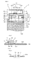
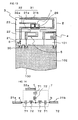
- Fig. 1 is a perspective view of an antenna device according to a first embodiment of the present invention.
- Fig. 2 is a plan view of the antenna device.
- Fig. 3 is a cross section as viewed in the direction of arrow A-A of Fig. 1 .
- an antenna device 1 of the present embodiment is a multisystem antenna device included in a wireless communication apparatus, such as a mobile phone or a PC card, and mounted on a circuit board 100 included in the wireless communication apparatus.
- the antenna device 1 is formed by providing a single dielectric base 2 on a non-ground region 101, which serves as an antenna mounting area, and mounting three antenna units 3, 4, and 5 on the dielectric base 2.
- the dielectric base 2 is integrally molded with dielectric material, positioned near an extremity of the antenna device 1 (i.e., on the upper side of Fig. 1 ), and secured to the non-ground region 101.
- the dielectric base 2 has a vertical front surface 21, a horizontal upper surface 22, an inclined surface 23 continuous with the upper surface 22 and extending downward toward the extremity of the antenna device 1. At the same time, the dielectric base 2 has a notch 20 on the boundary between the upper surface 22 and the inclined surface 23.
- the antenna unit 3 serves as a first antenna unit having the lowest fundamental frequency.
- the antenna unit 3 is an antenna for digital terrestrial television and has a fundamental frequency range of 470 MHz to 770 MHz.
- the antenna unit 3 includes a power feeder 30 and a radiation electrode 31 and is located at the left end of the non-ground region 101.
- a current-density control coil 6 serving as a current-density control circuit is connected in series between a base of the radiation electrode 31 and the power feeder 30, while a matching-circuit parallel coil 61 which is grounded is connected between the current-density control coil 6 and the power feeder 30.
- the current-density control coil 6 is provided to reduce current density between the base of the radiation electrode 31 and a reactance circuit 7 described below.
- the radiation electrode 31 is mostly formed on the dielectric base 2. Specifically, on the dielectric base 2, the radiation electrode 31 extends from the front surface 21 to the upper surface 22, passes inside the notch 20, and further extends up to the inclined surface 23. On the inclined surface 23, the radiation electrode 31 is bent to the right, extends downward along the right edge of the inclined surface 23 to the bottom end, and then extends leftward along the edge of the extremity of the inclined surface 23 until the tip of the radiation electrode 31 reaches the left corner at the extremity of the inclined surface 23.
- the reactance circuit 7 is disposed in the middle of the radiation electrode 31.
- the reactance circuit 7 is a circuit for varying the electric length of the radiation electrode 31 to adjust the frequency of the antenna unit 3.
- Fig. 4 is a circuit diagram illustrating the reactance circuit 7 of the present embodiment.
- the reactance circuit 7 to which the present embodiment is applied is a series resonant circuit including a capacitor 71 and an inductor 72.
- the reactance circuit 7 is formed on a dielectric substrate 70 and inserted into a recess 29 in the inclined surface 23 of the dielectric base 2.
- the recess 29 is located on the radiation electrode 31 and formed near the second point at which the current density of harmonics in the antenna unit 3 is highest. Therefore, as illustrated in Fig. 2 , the radiation electrode 31 is divided at the recess 29 into a base portion 31a near the base of the radiation electrode 31 and an extremity portion 31b near the extremity of the antenna device 1. Then, the dielectric substrate 70 on which the reactance circuit 7 is formed is inserted into the recess 29, an open end (located on the left in Fig.
- the capacitor 71 is connected to the base portion 31a of the radiation electrode 31, an open end (located on the right in Fig. 4 ) of the inductor 72 is connected to the extremity portion 31b of the radiation electrode 31, and thus the base and extremity portions 31a and 31b of the radiation electrode 31 are electrically connected to each other via the reactance circuit 7.
- the dielectric substrate 70 having the reactance circuit 7 formed thereon in a different process is inserted into the recess 29 of the dielectric base 2, and thus mounting of the reactance circuit 7 is simplified. Therefore, the capacitor 71 and the inductor 72, which are components of the reactance circuit 7, are hidden inside the recess 29 and do not protrude from the dielectric base 2. As a result, as illustrated in Fig. 1 and Fig. 3 , the shape of the dielectric base 2 can be determined without being limited by mounting of the reactance circuit 7.
- the upper surface of the dielectric base 2 is a bent surface including the upper surface 22 extending horizontally and the inclined surface 23 extending downward, and thus compactness of the antenna device 1 can be achieved.
- the antenna unit 4 illustrated in Fig. 1 serves as a second antenna unit having a fundamental frequency closest to the frequency of harmonics in the antenna unit 3.
- the antenna unit 4 is an antenna for global positioning system (GPS) communication and has a fundamental frequency of about 1575 MHz.
- GPS global positioning system
- the antenna unit 4 includes a power feeder 40 and a radiation electrode 41 and is located at the right end of the non-ground region 101. That is, to avoid interference caused by harmonics in the antenna unit 3, the antenna unit 4 is disposed at a position most distant from the antenna unit 3.
- the antenna unit 4 is a magnetic-field radiation antenna terminated with large capacitance by the non-ground region 101. An end of the radiation electrode 41 is grounded to the non-ground region 101 and power from the power feeder 40 is input via a capacitive part 42.
- the degree of coupling of a magnetic-field radiation antenna of this type with adjacent antennas is small. Therefore, when the antenna unit 4 is disposed away from the other antenna units, the degree of coupling can be further reduced.
- the radiation electrode 41 of the antenna unit 4 is also mostly formed on the dielectric base 2. Specifically, an electrode part 43 electrically connected to the power feeder 40 is formed at a right corner of the upper surface 22 of the dielectric base 2. With a base portion of the radiation electrode 41 disposed opposite the electrode part 43, the radiation electrode 41 extends toward the extremity of the antenna device 1 up to a right corner of the upper surface 22. Then, the radiation electrode 41 is bent to the left, extends further, and is bent back to the front. Then, the radiation electrode 41 extends downward along the front surface 21. Thus, the leading end of the radiation electrode 41 is electrically connected to a ground region 102 via a conductive trace 110 formed on the non-ground region 101.
- the antenna unit 5 serves as the other antenna unit having a fundamental frequency between the frequencies of the antenna unit 3 and the antenna unit 4.
- the antenna unit 5 is a dual-resonant antenna for evolution data only (EVDO) communication and has a fundamental frequency range of 843 MHz to 875 MHz and a frequency range of harmonics of 2.115 GHz to 2.130 GHz.
- EVDO evolution data only
- the antenna unit 5 includes a power feeder 50 and a radiation electrode 51 and is located on the left side of the non-ground region 101. That is, the antenna unit 5 is disposed between the antenna unit 3 and the antenna unit 4.
- the radiation electrode 51 of the antenna unit 5 is also mostly formed on the dielectric base 2. Specifically, while being connected to the power feeder 50, the radiation electrode 51 extends from a base of the front surface 21, the base being located at a lower end of the front surface 21. The radiation electrode 51 extends upward along the front surface 21, further extends straight along the upper surface 22 toward the extremity of the antenna device 1, and is bent to form an inverted C shape at one side of the notch 20 distant from the extremity of the antenna device 1.
- the capacitance of the radiation electrodes 31, 41, and 51 of the three antenna units 3, 4, and 5, respectively, is reduced by the notch 20.
- capacitance between the base portion 31a of the radiation electrode 31 and the radiation electrode 51 is reduced by a left portion of the notch 20, while capacitance between the extremity portion 31b of the radiation electrode 31 and the radiation electrode 41 is reduced by a right portion of the notch 20.
- most parts of the radiation electrodes 31, 41, and 51 of the antenna units 3, 4, and 5, respectively, are formed on the single dielectric base 2. This not only reduces manufacturing costs, but also simplifies the manufacturing process.
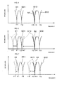
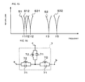
- Fig. 5 is a graph showing return losses of antenna units in a state where the current-density control coil 6 and the reactance circuit 7 are not present.
- Fig. 6 is a graph showing return losses of the antenna units in a state where adjustment is made by the current-density control coil 6.
- Fig. 7 is a graph showing return losses of the antenna units in a state where adjustment is made by the current-density control coil 6 and the reactance circuit 7.
- the antenna unit 3 can be used at a fundamental frequency f1 in the 470 MHz to 770 MHz range (return loss curve S1), the antenna unit 4 can be used at a fundamental frequency f3 of about 1575 MHz (return loss curve S2), and the antenna unit 5 can be used at a frequency f2 in the 843 MHz to 875 MHz range (return loss curve S31) and at a frequency f5 in the 2.115 GHz to 2.130 GHz range (return loss curve S32).
- a communication apparatus such as a mobile phone, including the antenna device 1 of the present embodiment
- the fundamental frequency f1 of the antenna unit 3 and the frequency f2 of the antenna unit 5 are close to each other.
- the antenna units 3 and 5 may be strongly electrically coupled to each other, and thus antenna gain may be degraded.
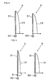
- Fig. 8 is a schematic view showing distributions of current densities at the fundamental frequencies of the antenna unit 3 and antenna unit 5.
- Fig. 9 is a schematic view showing distributions of current densities adjusted by the current-density control coil 6.
- the antenna units 3 and 5 having close fundamental frequencies exhibit similar distributions of high current densities I3 and I5.
- the current densities I3 and I5 in base parts of the radiation electrodes 31 and 51 i.e., in portions of the radiation electrodes 31 and 51, the portions being formed on the front surface 21 of the dielectric base 2) are high, currents that flow through these base parts cause magnetic field coupling between the radiation electrodes 31 and 51.
- the radiation electrode 31 is provided with the current-density control coil 6. Therefore, it is possible to set the inductance value of the current-density control coil 6 such that the current density in the radiation electrode 31 is reduced.
- the current density I3 in the radiation electrode 31 becomes smaller than the current density I5 in the radiation electrode 51 of the antenna unit 5, and magnetic field coupling between the radiation electrodes 31 and 51 can be prevented.
- harmonics (return loss curve S13) having a frequency f4 that is three times the fundamental frequency f1 are generated and may interfere with the antenna unit 4 having the fundamental frequency f3 closest to the frequency f4 of the harmonics.
- Fig. 10 is a schematic view for illustrating an interference phenomenon caused by harmonics.
- the current density I3 of harmonics in the antenna unit 3 is high.
- the current density I3 for the frequency f4 of the harmonics and a current density I4 for the fundamental frequency f3 of the antenna unit 4 cause strong coupling of magnetic fields.
- a maximum electric field point P appears at the base of the radiation electrode 31. Therefore, if the antenna units 3 and 4 are located close to each other, the degree of coupling between the electric field E3 of the harmonics and an electric field E4 of the antenna unit 4 is high.
- the antenna unit 4 since the antenna unit 4 is disposed at a position most distant from the antenna unit 3, adverse effects of such electric fields and magnetic fields can be reduced.
- the antenna unit 4 may be affected by the harmonics in the antenna unit 3.
- the current-density control coil 6 is provided to allow the fundamental frequency f1 to be slightly shifted. Therefore, accordingly, the frequency f4 is shifted away from the fundamental frequency f3.
- the frequency f4 is shifted by an amount as much as three times the amount of shift of the fundamental frequency f1. Therefore, if the current-density control coil 6 lowers the fundamental frequency f1, the frequency f4 of the harmonics approaches a frequency f4' near the frequency f2, as indicated by a dashed line in Fig. 6 , and thus may cause interference. However, if the fundamental frequency f1 is lowered by an amount that does not cause the frequency f4 to approach the frequency f2, a current density in the power feeder cannot be reduced. Therefore, magnetic field coupling between the antenna unit 3 and the antenna unit 5 cannot be avoided. In other words, the fundamental frequency f1 of the antenna unit 3 and the frequency f4 cannot be simultaneously shifted to their respective desired values only by the current-density control coil 6.
- the reactance circuit 7 is provided in the middle of the radiation electrode 31 of the antenna unit 3. Therefore, by setting a reactance value of the reactance circuit 7 to a desired value, the amount of shift of the frequency f4 of harmonics can be adjusted.
- the reactance circuit 7 when configured as a series resonant circuit including the capacitor 71 and the inductor 72, different reactance values can be provided for respective frequencies, and thus the frequency f4 of harmonics can be lowered by a desired amount. Therefore, as shown in Fig. 7 , the fundamental frequency f1 of the antenna unit 3 can be sufficiently shifted away from the frequency f2 of the antenna unit 5, and the frequency f4 of harmonics can be shifted to the frequency f4' that is sufficiently distant from the frequency f2 of the antenna unit 5 and is not close to the frequency f2 of the antenna unit 5. As a result, interference caused by harmonics of the antenna unit 3 can be substantially completely avoided.
- the three antenna units 3 to 5 can be densely mounted in a small antenna mounting area without interference among them.
- high-density mounting of components and compactness of the antenna device 1 can be achieved.
- a series resonant circuit including the capacitor 71 and the inductor 72 is used as the reactance circuit 7.
- a parallel resonant circuit including the capacitor 71 and the inductor 72 may be used as the reactance circuit 7.
- the frequency f4 of harmonics in the antenna unit 3 can be shifted to lower values, as shown in Fig. 7 .
- the frequency f4 of harmonics in the antenna unit 3 can be shifted to higher values, as shown in Fig. 12 . Therefore, depending on the arrangement of a plurality of antenna units of the antenna device 1, either one of a series resonant circuit and a parallel resonant circuit can be used as the reactance circuit 7.
- the reactance circuit 7 may be either a series resonant circuit or a parallel resonant circuit, as long as the circuit includes one or more capacitors and one or more inductors, and is not limited to one specific series resonant circuit or parallel resonant circuit.
- a reactance circuit formed by combining the series resonant circuit of Fig. 4 and the parallel resonant circuit of Fig. 11 may also be used as the reactance circuit 7.
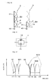
- Fig. 13 is a plan view of an antenna device according to the second embodiment of the present invention.
- Fig. 14 is a circuit diagram illustrating the reactance circuit 7 of the second embodiment.
- the antenna device of the present embodiment is different from that of the first embodiment in that a branched radiation electrode 32a is added to the antenna unit 3.
- the branched radiation electrode 32a is horizontally formed on the inclined surface 23 of the dielectric base 2 and connected to the reactance circuit 7. Then, the reactance circuit 7 is configured to allow the branched radiation electrode 32a to be connected to the base portion 31a of the radiation electrode 31.
- each series resonant circuit including the capacitor 71 and the inductor 72 are connected to each other.
- another series resonant circuit having the same configuration as that of the other two series resonant circuits is connected to a point of connection between the two series resonant circuits to form the reactance circuit 7.
- the base portion 31a of the radiation electrode 31, the extremity portion 31b of the radiation electrode 31, and the branched radiation electrode 32a are connected to three open ends a, b, and c, respectively.
- a radiation electrode 32 including the base portion 31a of the radiation electrode 31 and the branched radiation electrode 32a is connected to the power feeder 30, and thus the antenna unit 3 of dual-resonant type is formed.
- Fig. 15 is a graph showing return losses of the antenna units in the antenna device of the present embodiment.
- a frequency f12 (return loss curve S12) between the fundamental frequency f1 (return loss curve S1) and the fundamental frequency f3 of the antenna unit 4, as well as the fundamental frequency f1, can be obtained.
- the bandwidth of the antenna unit 3 can thus be increased, a wideband antenna device can be realized. Although a size reduction of an antenna unit may lead to a narrow bandwidth, such a disadvantage can be overcome by increasing the bandwidth of the antenna unit, as in the case of the present embodiment.
- a series resonant circuit formed by combining three series resonant circuits, each including the capacitor 71 and the inductor 72, is used as the reactance circuit 7.
- a parallel resonant circuit formed by combining three parallel resonant circuits, each including the capacitor 71 and the inductor 72 may be used as the reactance circuit 7, so that the amount of change in the reactance value of the reactance circuit 7 can be increased.
- the reactance circuit 7 may be either a series resonant circuit or a parallel resonant circuit, as long as the circuit includes one or more capacitors and one or more inductors.
- a reactance circuit formed by combining the series resonant circuit of Fig. 14 and the parallel resonant circuit of Fig. 16 may also be used as the reactance circuit 7.
- Fig. 17 is a plan view of an antenna device according to the third embodiment of the present invention.
- Fig. 18 is a partial enlarged cross-sectional view of the antenna device.
- the present embodiment is different from the second embodiment in that the branched radiation electrode 32a is disposed not on the inclined surface 23 of the dielectric base 2, but on any exposed surface.
- the branched radiation electrode 32a is horizontally disposed on an exposed surface 24 which is an exposed surface of the dielectric base 2 and on which the radiation electrodes 31, 41, and 51 of the antenna units 3, 4, and 5, respectively, are not disposed. Then, a conductive path 121 is connected to the open end c (see Fig. 16 ) of the reactance circuit 7, extends from the bottom of the recess 29 to the exposed surface 24 which is an inner surface of the notch 20, and then is connected to an end of the branched radiation electrode 32a.
- the branched radiation electrode 32a is disposed on the surface where the radiation electrodes 31, 41, and 51 are not disposed, the degree of freedom of arrangement of the branched radiation electrode 32a is increased.
- the branched radiation electrode 32a is disposed on the exposed surface 24 of the dielectric base 2. However, as indicated by dashed lines in Fig. 18 , the branched radiation electrode 32a may be disposed on an exposed surface 25 opposite the exposed surface 24 and connected to the reactance circuit 7 via a conductive path 122.
- the extremity portion 31b of the radiation electrode 31 and the like may also be disposed on any exposed surface.
- Fig. 19 is a plan view of an antenna device according to the fourth embodiment of the present invention.
- Fig. 20 is a circuit diagram illustrating the reactance circuit 7 of the present embodiment.
- the present embodiment is different from the second embodiment in that a variable capacitance element is included in the reactance circuit.
- a reactance circuit 7' including variable capacitance elements is inserted into the recess 29 to form a dual-resonant structure.
- Vc control voltage
- a direct-current power supply 60 for the control voltage Vc is connected to a connection point d of the three inductors 72 via a resistor 73 for cutting harmonics.
- Reference numeral 74 denotes a capacitor for allowing harmonics to pass through.
- the antenna device of the present embodiment is a dual-resonant antenna in which resonance occurs, via the reactance circuit 7', in the antenna unit including the base portion 31a and extremity portion 31b of the radiation electrode 31 and the power feeder 30 and in the antenna unit including the base portion 31a of the radiation electrode 31, the branched radiation electrode 32a, and the power feeder 30.
- the capacitance values of the respective variable capacitance capacitors 71' can be varied, and thus the electrical length of the radiation electrode 31 including the base portion 31a and the extremity portion 31b and the electrical length of the radiation electrode 32 including the base portion 31a of the radiation electrode 31 and the branched radiation electrode 32a can be varied.
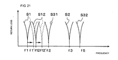
- Fig. 21 is a graph for illustrating frequency changes associated with use of the reactance circuit 7'.
- the fundamental frequency f1 (return loss curve S1) and the frequency f12 (return loss curve S12) for dual-resonance can be shifted to a fundamental frequency f1' and a frequency f12', respectively, as indicated by dashed lines in Fig. 21 .
- the antenna device of the present embodiment since frequencies can be changed even after insertion of the reactance circuit 7' into the recess 29, an individual adjustment corresponding to each product can be made. At the same time, since the fundamental frequency f1 and the frequency f2 for dual-resonance can be varied, a bandwidth wider than that of the antenna device of the second embodiment can be ensured.
- the reactance circuit 7' is composed of three series resonant circuits, each including the variable capacitance capacitor 71' and the inductor 72.
- the reactance circuit 7' may be composed of three parallel resonant circuits, each including the variable capacitance capacitor 71' and the inductor 72.
- the reactance circuit 7' may be formed by combining series and parallel resonant circuits.
- any one or more capacitors in the reactance circuit are replaced with one or more variable capacitance elements, such as the variable capacitance capacitors 71'
- the reactance value of the reactance circuit can be changed by application of a control voltage.
- one or two capacitors 71 may be replaced with one or two variable capacitance capacitors 71'.
- variable capacitance capacitor 71' a variable capacitance diode, a micro electro mechanical systems (MEMS) element, a barium-strontium-titanate (BST (ferroelectric material)) element, or the like may be used as a variable capacitance element.
- MEMS micro electro mechanical systems
- BST barium-strontium-titanate
- the non-ground region 101 serves as an antenna mounting area
- the dielectric base 2 is mounted on the non-ground region 101.
- the antenna mounting area refers not only to the non-ground region, but also refers to all mounting areas including the ground region 102. Therefore, an invention in which antenna units for different systems are disposed on the backside of the non-ground region 101 and/or on the ground region 102 is also included in the scope of the present invention.
- the radiation electrodes 31, 41, and 51 of the antenna units 3, 4, and 5, respectively, and the branched radiation electrode 32a are mostly formed on the dielectric base 2.
- an invention of an antenna device in which the radiation electrodes 31, 41, and 51 of the antenna units 3, 4, and 5, respectively, and the branched radiation electrode 32a are partially formed on the dielectric base 2 and mostly formed, as a pattern, on the non-ground region 101 and the like may also included in the scope of the present invention.
- the radiation electrode 31 and the like are formed on the single dielectric base 2.
- an invention in which radiation electrodes of respective antenna units are formed on a plurality of different dielectric bases is not to be excluded from the scope of the present invention.
- the three antenna units 3 to 5 are mounted in the embodiments described above, an invention of an antenna device in which four or more antenna units corresponding to four or more different systems are mounted is also within the scope of the present invention.
- the current-density control coil 6 is used as a current-density control circuit in the embodiments described above, any circuit capable of controlling the current density in the antenna unit 3 can be used.
- a magnetic-field radiation antenna is used as the antenna unit 4 serving as a second antenna unit.
- the type of antenna is not limited to this. Any type of antenna, including a monopole antenna, can be used as the antenna unit 4.
- branched radiation electrode 32a Although one branched radiation electrode 32a is added in the second to fourth embodiments described above, it should be understood that the number of branched radiation electrodes is not limited to this.
Abstract
Description
- The present invention relates to frequency-adjustable antenna devices, and particularly to an antenna device and a wireless communication apparatus for multisystem communication.
- Examples of known techniques relating to antenna devices of this type are described in
Patent Document 1 andPatent Document 2. -
Patent Document 1 describes a frequency variable antenna having a loop-shaped radiation electrode that performs a monopole antenna operation. The frequency variable antenna is provided with a frequency variable circuit in the middle of the radiation electrode. Thus, by externally applying a voltage to the frequency variable circuit to vary a reactance component of the frequency variable circuit, it is possible to vary the frequency while maintaining good gain. -
Patent Document 2 describes an antenna device having an antenna main body and a variable capacitance diode that forms a resonant circuit at a base of the antenna main body. By applying a tuning voltage to vary the electrostatic capacitance of the variable capacitance diode, a desired frequency can be obtained. - Recently, as mobile phones have become multifunctional, it has become necessary to mount various systems of different frequencies on the same substrate. To realize such a multifunctional mobile phone, it is necessary to mount many antenna units corresponding to various systems close together in a small antenna mounting area.
- However, when a plurality of antenna units are mounted, if antenna units having close fundamental frequencies are located close together or if a first antenna unit and a second antenna unit having a fundamental frequency close to a frequency of harmonics in the first antenna unit are located close together, interference may occur and cause degradation in characteristics of these antenna units.
- However, because of enhanced multifunctionality of mobile phones, since a substrate is mostly occupied by functional circuits other than radiation electrodes of antenna units, a mounting area for mounting the radiation electrodes is reduced. At the same time, as the size of mobile phones shrinks, a mounting area for mounting radiation electrodes becomes extremely small.
- Thus, under circumstances where it is necessary to mount radiation electrodes of antenna units for various systems in a very small area, antenna units having close frequencies need to be arranged close together.
- Therefore, it is hoped that there will be developed an antenna device in which no interference occurs even if many antenna units corresponding to various systems are mounted close together in a small area.
- Patent Document 1: PCT International Publication No.
WO2004/109850 - Patent Document 2: Japanese Unexamined Patent Application Publication No.
2002-232313 - However, with the foregoing known techniques, it is difficult to meet the expectation described above.
- Specifically, in the frequency variable antenna described in
Patent Document 1, a current density in a radiation electrode extending from a power feeder to a frequency variable circuit is very high. Therefore, if a number of such antennas are arranged close together, currents flowing through bases of antennas having close fundamental frequencies may cause very strong coupling of magnetic fields, and interference may occur between these antennas. This may result in deterioration in isolation between antennas and degradation of antenna gain. - Additionally, since components are mounted on a surface of a substrate to form a frequency variable circuit, these components protrude from the surface of the substrate by the thicknesses of these components. This not only hinders a size reduction in the direction of thickness of the mobile phone, but also causes a problem of strength of component mounting.
- In the antenna device described in
Patent Document 2, current densities of both fundamental waves and harmonics are very high at the base of the antenna main body. Therefore, by increasing the inductance of a matching circuit at the base of the antenna main body, fundamental waves and harmonics can be changed simultaneously. However, if a fundamental frequency is changed, the frequency of the corresponding harmonics is changed by an amount as much as several times greater than the amount of change of the fundamental frequency. Thus, since fundamental waves and harmonics cannot be independently controlled, the frequency of the harmonics may overlap with the fundamental frequency of another system, and thus, mutual interference may occur. - Thus, with the techniques described in
Patent Documents - Moreover, in the techniques described above, when many antenna units are put together in one place, radiation electrodes and the like of the respective antenna units are disposed on different substrates. This means that costs involved in forming a radiation electrode and the like on each substrate are multiplied by the number of antenna units. Additionally, when antenna units individually designed are integrated into one place, since their characteristics may be changed depending on the installation conditions, each antenna unit needs to be adjusted in response to the changes in characteristics. This makes the process more complicated.
- The present invention has been made to solve the problems described above. An object of the present invention is to provide a compact and low-cost antenna device in which no interference occurs even if many antenna units corresponding to various systems are mounted close together in a small area, and further to provide a wireless communication apparatus including the antenna device.
- To solve the problems described above, an antenna device according to
Claim 1 of the present invention includes a plurality of antenna units each having a power feeder and a radiation electrode, a circuit board having an antenna mounting area on which the plurality of antenna units are mounted, and a dielectric base on which the whole or part of the radiation electrodes of the respective antenna units is formed. Of the plurality of antenna units, a first antenna unit having a lowest fundamental frequency is disposed at an end of the antenna mounting area, a second antenna unit having a fundamental frequency closest to a frequency of harmonics in the first antenna unit is disposed more distantly from the first antenna unit than the other one or more antenna units are from the first antenna unit, and the other one or more antenna units are interposed between the first and second antenna units in parallel therewith. A current-density control circuit capable of controlling a current density in the radiation electrode is interposed between the radiation electrode and the power feeder of the first antenna unit, while a reactance circuit for adjusting a frequency by varying an electrical length of the radiation electrode of the first antenna unit is disposed in the middle of the radiation electrode of the first antenna unit. - With this configuration, the plurality of antenna units allow communication in different systems. Specifically, the first antenna unit allows communication at lowest frequencies, the second antenna unit allows communication at higher frequencies, and the other one or more antenna units allow communication at the other frequencies.
- When communication is performed using the first antenna unit, if the power feeder of one of the other one or more antenna units having a fundamental frequency close to that of the first antenna unit is located close to the first antenna unit, since current densities at the basis of the radiation electrodes of the respective antenna units are high, the currents may cause magnetic field coupling, and thus, the performance of the first antenna unit and the antenna gain of the first antenna unit may be degraded.
- However, in the present invention, the current-density control circuit is disposed between the radiation electrode and the power feeder of the first antenna unit. With the current-density control circuit, it is possible to set such that the current density in the radiation electrode is reduced. Thus, magnetic field coupling between the first antenna unit and the other antenna unit close to the first antenna unit can be prevented. Therefore, by providing the first antenna unit at an end of the antenna mounting area and providing the other antenna unit near the power feeder of the first antenna unit, many antenna units can be mounted within a small antenna mounting area.
- In the second antenna unit having a fundamental frequency greatly different from that of the first antenna unit but closest to the frequency of harmonics in the first antenna unit, the harmonics in the first antenna unit may cause electric and magnetic field coupling. Therefore, the second antenna unit is disposed more distantly from the first antenna unit than the other one or more antenna units are from the first antenna unit. However, depending on the size of the antenna mounting area, the distance between the first antenna unit and the second antenna unit may not be sufficient. As a result, the second antenna unit may be electrically coupled with harmonics in the first antenna unit.
- However, in the present invention, the reactance circuit is disposed in the middle of the radiation electrode of the first antenna unit. With the reactance circuit, it is possible to set such that the frequency of harmonics in the first antenna unit is separated from the fundamental frequency of the second antenna unit. Thus, electrical coupling between the first antenna unit and the second antenna unit can be prevented.
- According to
Claim 2 of the present invention, in the antenna device described inClaim 1, the whole or part of the radiation electrodes of the respective antenna units is formed on the single dielectric base, while one or more notches for reducing capacitance between radiation electrodes of any of the first antenna unit, the second antenna unit, and the other one or more antenna units are disposed at a portion of the dielectric base and between the radiation electrodes. - With this configuration, since the whole or part of the radiation electrodes of the respective antenna units is formed on the single dielectric base, the manufacturing costs can be made lower than those in the case where the radiation electrodes of the respective antenna units are disposed on different dielectric bases. Moreover, since there is no need for adjustment of each antenna unit, a simple manufacturing process can be realized. At the same time, since capacitance between the radiation electrodes by which the one or more notches are interposed is reduced, interference between these radiation electrodes can be reduced.
- According to
Claim 3 of the present invention, in the antenna device described inClaim 1 orClaim 2, a recess is provided on a surface of the dielectric base, and a substrate on which the reactance circuit is formed is disposed inside the recess. - In this configuration, components are mounted on the substrate in a different process to form the reactance circuit, and then, the substrate is inserted into the recess on the surface of the dielectric base. Therefore, the reactance circuit can be easily mounted in the middle of the radiation electrode of the first antenna unit. With this configuration, the components of the reactance circuit are hidden inside the recess and do not protrude from the dielectric base. Also, mounting on the curved surface of the dielectric base is made possible.
- According to
Claim 4 of the present invention, in the antenna device described in any one ofClaim 1 toClaim 3, the current-density control circuit is a current-density control coil connected in series between the power feeder and the radiation electrode of the first antenna unit. - With this configuration, magnetic field coupling between the first antenna unit and another antenna unit having a fundamental frequency close to that of the first antenna unit can be prevented with a simple structure.
- According to
Claim 5 of the present invention, in the antenna device described in any one ofClaim 1 to Claim 4, the reactance circuit is a series resonant circuit or a parallel resonant circuit and includes one or more capacitors and one or more inductors. - With this configuration, in which a series resonant circuit or a parallel resonant circuit is used as the reactance circuit, high impedance can be applied to the radiation electrode of the first antenna unit at specific frequencies. Thus, it is possible to effectively control the frequency of harmonics produced in the first antenna unit.
- According to
Claim 6 of the present invention, in the antenna device described inClaim 5, any or all of the one or more capacitors in the reactance circuit are replaced with one or more variable capacitance elements, and a control voltage is applied to vary each capacitance value of the one or more variable capacitance elements, and thus vary a reactance value of the reactance circuit. - In this configuration, after the reactance circuit is mounted inside the recess, a control voltage is applied to the one or more variable capacitance elements, and thus the electrical length of the radiation electrode of the first antenna unit can be freely changed.
- According to
Claim 7 of the present invention, in the antenna device described in any one ofClaim 1 to Claim 6, one or more branched radiation electrodes are branched from the radiation electrode of the first antenna unit via the reactance circuit, and the whole or part of the one or more branched radiation electrodes is disposed on the dielectric base. - With this configuration, the first antenna unit can serve as a multi-resonant antenna, and the number of fundamental frequencies that can be obtained from a single power feeder increases.
- According to Claim 8 of the present invention, in the antenna device described in any one of
Claim 1 to Claim 7, a portion of the radiation electrode of the first antenna unit, the portion extending from the reactance circuit and being adjacent to an extremity of the antenna device, or any of the one or more branched radiation electrodes is disposed on an exposed surface of the dielectric base, and the portion of the radiation electrode or the branched radiation electrode is electrically connected to the reactance circuit via a conductive path extending from a bottom of the recess to the exposed surface. - With this configuration, part of the radiation electrode of the first antenna unit or the branched radiation electrode can be disposed on an exposed surface different from the surface where the radiation electrode is disposed.
- A wireless communication apparatus according to Claim 9 of the present invention includes the antenna device according to any one of
Claim 1 to Claim 8. - As described above in detail, in the antenna device of the present invention, since the current-density control circuit makes it possible to reduce a current density in the radiation electrode of the first antenna unit, it is possible to prevent magnetic field coupling between the first antenna unit and another antenna unit having a fundamental frequency close to that of the first antenna unit. Additionally, since the second antenna unit having a fundamental frequency close to the frequency of harmonics in the first antenna unit is disposed at a position most distant from the first antenna unit and, at the same time, the reactance circuit is provided, interference between the first and second antenna units can be prevented. Therefore, many antenna units can be densely mounted on a small antenna mounting area. This has an excellent effect of realizing a high-density and compact antenna device.
- According to
Claim 2 of the present invention, since the whole or part of the radiation electrodes of the respective antenna units is formed on the single dielectric base, reduced manufacturing costs and an easier manufacturing process can be realized. Additionally, the one or more notches make it possible to effectively reduce interference between radiation electrodes. - According to
Claim 3 of the present invention, unlike the case where components are directly mounted on the surface of the dielectric base, even if the surface of the dielectric base is curved, the substrate having the reactance circuit thereon can be easily mounted on the surface of the dielectric base. Moreover, since the components do not protrude from the dielectric base, the dielectric base can be shaped to match the shape of terminal equipment without being limited by mounting of the reactance circuit, and thus a compact antenna device can be realized. - According to
Claim 4 of the present invention, magnetic field coupling between the first antenna unit and another antenna unit having a fundamental frequency close to that of the first antenna unit can be prevented with a simple structure. - According to
Claim 5 of the present invention, it is possible to effectively control the frequency of harmonics produced in the first antenna unit. - According to
Claim 6 of the present invention, by applying a control voltage to the one or more variable capacitance elements, the electrical length of the radiation electrode of the first antenna unit can be freely changed. Therefore, with the reactance circuit, it is possible to compensate for a reduction in bandwidth associated with a reduction in size of the antenna device, and thus to provide a compact antenna device having a wide bandwidth. - According to
Claim 7 of the present invention, since the first antenna unit can be configured as a multi-resonant antenna, the number of power feeders becomes smaller than that of radiation electrodes. This makes it possible to increase the distance between power feeders and reduce coupling between radiation elements. Additionally, since the first antenna unit configured as a multi-resonant antenna has a wider bandwidth, it is possible to provide a compact and wideband antenna device. - According to Claim 8 of the present invention, since part of the radiation electrode of the first antenna unit or the branched radiation electrode can be disposed on any exposed surface different from the surface where the radiation electrode is disposed, it is possible to increase the degree of freedom of arrangement of the branched radiation electrode and the like, further reduce the size of the antenna device, improve antenna efficiency, and reduce interference between antenna units.
- According to Claim 9 of the present invention, it is possible to provide a compact and high-density wireless communication apparatus capable of performing multisystem communication.
-
-
Fig. 1 is a perspective view of an antenna device according to a first embodiment of the present invention. -
Fig. 2 is a plan view of the antenna device. -
Fig. 3 is a cross section as viewed in the direction of arrow A-A ofFig. 1 . -
Fig. 4 is a circuit diagram illustrating a reactance circuit of the first embodiment. -
Fig. 5 is a graph showing return losses of antenna units in a state where a current-density control coil and the reactance circuit are not present. -
Fig. 6 is a graph showing return losses of the antenna units in a state where adjustment is made by the current-density control coil. -
Fig. 7 is a graph showing return losses of the antenna units in a state where adjustment is made by the current-density control coil and the reactance circuit. -
Fig. 8 is a schematic view showing distributions of current densities at the fundamental frequencies of the antenna units. -
Fig. 9 is a schematic view showing distributions of current densities adjusted by the current-density control coil. -
Fig. 10 is a schematic view for illustrating an interference phenomenon caused by harmonics. -
Fig. 11 is a circuit diagram illustrating a modification of the reactance circuit used in the first embodiment. -
Fig. 12 is a graph for illustrating changes in harmonics, the changes being associated with use of a parallel resonant circuit. -
Fig. 13 is a plan view of an antenna device according to a second embodiment of the present invention. -
Fig. 14 is a circuit diagram illustrating a reactance circuit of the second embodiment. -
Fig. 15 is a graph showing return losses of antenna units in the antenna device of the second embodiment. -
Fig. 16 is a circuit diagram illustrating a modification of the reactance circuit used in the second embodiment. -
Fig. 17 is a plan view of an antenna device according to a third embodiment of the present invention. -
Fig. 18 is a partial enlarged cross-sectional view of the antenna device. -
Fig. 19 is a plan view of an antenna device according to a fourth embodiment of the present invention. -
Fig. 20 is a circuit diagram illustrating a reactance circuit of the fourth embodiment. -
Fig. 21 is a graph for illustrating frequency changes associated with use of the reactance circuit of the fourth embodiment. -
- 1: antenna device
- 2: dielectric base
- 3 to 5: antenna unit
- 6: current-density control coil
- 7, 7': reactance circuit
- 20: notch
- 21: front surface
- 22: upper surface
- 23: inclined surface
- 24, 25: exposed surface
- 29: recess
- 30, 40, 50: power feeder
- 31, 32, 41, 51: radiation electrode
- 31a: base portion of radiation electrode
- 31b: extremity portion of radiation electrode
- 32a: branched radiation electrode
- 60: direct-current power supply
- 70: dielectric substrate
- 71: capacitor
- 71': variable capacitance capacitor
- 72: inductor
- 73: resistor
- 100: circuit board
- 101: non-ground region
- 102: ground region
- Vc: control voltage
- Best modes for carrying out the present invention will now be described with reference to the drawings.
-
Fig. 1 is a perspective view of an antenna device according to a first embodiment of the present invention.Fig. 2 is a plan view of the antenna device.Fig. 3 is a cross section as viewed in the direction of arrow A-A ofFig. 1 . - As illustrated in
Fig. 1 , anantenna device 1 of the present embodiment is a multisystem antenna device included in a wireless communication apparatus, such as a mobile phone or a PC card, and mounted on acircuit board 100 included in the wireless communication apparatus. - Specifically, the
antenna device 1 is formed by providing asingle dielectric base 2 on anon-ground region 101, which serves as an antenna mounting area, and mounting threeantenna units dielectric base 2. - The
dielectric base 2 is integrally molded with dielectric material, positioned near an extremity of the antenna device 1 (i.e., on the upper side ofFig. 1 ), and secured to thenon-ground region 101. - Specifically, the
dielectric base 2 has a verticalfront surface 21, a horizontalupper surface 22, aninclined surface 23 continuous with theupper surface 22 and extending downward toward the extremity of theantenna device 1. At the same time, thedielectric base 2 has anotch 20 on the boundary between theupper surface 22 and theinclined surface 23. - Of the three antenna units, the
antenna unit 3 serves as a first antenna unit having the lowest fundamental frequency. In the present embodiment, theantenna unit 3 is an antenna for digital terrestrial television and has a fundamental frequency range of 470 MHz to 770 MHz. - As illustrated in
Fig. 1 andFig. 2 , theantenna unit 3 includes apower feeder 30 and aradiation electrode 31 and is located at the left end of thenon-ground region 101. - Specifically, a current-
density control coil 6 serving as a current-density control circuit is connected in series between a base of theradiation electrode 31 and thepower feeder 30, while a matching-circuit parallel coil 61 which is grounded is connected between the current-density control coil 6 and thepower feeder 30. The current-density control coil 6 is provided to reduce current density between the base of theradiation electrode 31 and areactance circuit 7 described below. - The
radiation electrode 31 is mostly formed on thedielectric base 2. Specifically, on thedielectric base 2, theradiation electrode 31 extends from thefront surface 21 to theupper surface 22, passes inside thenotch 20, and further extends up to theinclined surface 23. On theinclined surface 23, theradiation electrode 31 is bent to the right, extends downward along the right edge of theinclined surface 23 to the bottom end, and then extends leftward along the edge of the extremity of theinclined surface 23 until the tip of theradiation electrode 31 reaches the left corner at the extremity of theinclined surface 23. - The
reactance circuit 7 is disposed in the middle of theradiation electrode 31. Thereactance circuit 7 is a circuit for varying the electric length of theradiation electrode 31 to adjust the frequency of theantenna unit 3. -
Fig. 4 is a circuit diagram illustrating thereactance circuit 7 of the present embodiment. - As illustrated in
Fig. 4 , thereactance circuit 7 to which the present embodiment is applied is a series resonant circuit including acapacitor 71 and aninductor 72. - As illustrated in
Fig. 2 and Fig. 3 , thereactance circuit 7 is formed on adielectric substrate 70 and inserted into arecess 29 in theinclined surface 23 of thedielectric base 2. Specifically, therecess 29 is located on theradiation electrode 31 and formed near the second point at which the current density of harmonics in theantenna unit 3 is highest. Therefore, as illustrated inFig. 2 , theradiation electrode 31 is divided at therecess 29 into a base portion 31a near the base of theradiation electrode 31 and anextremity portion 31b near the extremity of theantenna device 1. Then, thedielectric substrate 70 on which thereactance circuit 7 is formed is inserted into therecess 29, an open end (located on the left inFig. 4 ) of thecapacitor 71 is connected to the base portion 31a of theradiation electrode 31, an open end (located on the right inFig. 4 ) of theinductor 72 is connected to theextremity portion 31b of theradiation electrode 31, and thus the base andextremity portions 31a and 31b of theradiation electrode 31 are electrically connected to each other via thereactance circuit 7. - In the present embodiment, as described above, the
dielectric substrate 70 having thereactance circuit 7 formed thereon in a different process is inserted into therecess 29 of thedielectric base 2, and thus mounting of thereactance circuit 7 is simplified. Therefore, thecapacitor 71 and theinductor 72, which are components of thereactance circuit 7, are hidden inside therecess 29 and do not protrude from thedielectric base 2. As a result, as illustrated inFig. 1 andFig. 3 , the shape of thedielectric base 2 can be determined without being limited by mounting of thereactance circuit 7. In the present embodiment, the upper surface of thedielectric base 2 is a bent surface including theupper surface 22 extending horizontally and theinclined surface 23 extending downward, and thus compactness of theantenna device 1 can be achieved. - The
antenna unit 4 illustrated inFig. 1 serves as a second antenna unit having a fundamental frequency closest to the frequency of harmonics in theantenna unit 3. In the present embodiment, theantenna unit 4 is an antenna for global positioning system (GPS) communication and has a fundamental frequency of about 1575 MHz. - As illustrated in
Fig. 1 andFig. 2 , theantenna unit 4 includes apower feeder 40 and aradiation electrode 41 and is located at the right end of thenon-ground region 101. That is, to avoid interference caused by harmonics in theantenna unit 3, theantenna unit 4 is disposed at a position most distant from theantenna unit 3. - The
antenna unit 4 is a magnetic-field radiation antenna terminated with large capacitance by thenon-ground region 101. An end of theradiation electrode 41 is grounded to thenon-ground region 101 and power from thepower feeder 40 is input via acapacitive part 42. The degree of coupling of a magnetic-field radiation antenna of this type with adjacent antennas is small. Therefore, when theantenna unit 4 is disposed away from the other antenna units, the degree of coupling can be further reduced. - The
radiation electrode 41 of theantenna unit 4 is also mostly formed on thedielectric base 2. Specifically, anelectrode part 43 electrically connected to thepower feeder 40 is formed at a right corner of theupper surface 22 of thedielectric base 2. With a base portion of theradiation electrode 41 disposed opposite theelectrode part 43, theradiation electrode 41 extends toward the extremity of theantenna device 1 up to a right corner of theupper surface 22. Then, theradiation electrode 41 is bent to the left, extends further, and is bent back to the front. Then, theradiation electrode 41 extends downward along thefront surface 21. Thus, the leading end of theradiation electrode 41 is electrically connected to aground region 102 via aconductive trace 110 formed on thenon-ground region 101. - The
antenna unit 5 serves as the other antenna unit having a fundamental frequency between the frequencies of theantenna unit 3 and theantenna unit 4. In the present embodiment, theantenna unit 5 is a dual-resonant antenna for evolution data only (EVDO) communication and has a fundamental frequency range of 843 MHz to 875 MHz and a frequency range of harmonics of 2.115 GHz to 2.130 GHz. - As illustrated in
Fig. 1 andFig. 2 , theantenna unit 5 includes apower feeder 50 and aradiation electrode 51 and is located on the left side of thenon-ground region 101. That is, theantenna unit 5 is disposed between theantenna unit 3 and theantenna unit 4. - The
radiation electrode 51 of theantenna unit 5 is also mostly formed on thedielectric base 2. Specifically, while being connected to thepower feeder 50, theradiation electrode 51 extends from a base of thefront surface 21, the base being located at a lower end of thefront surface 21. Theradiation electrode 51 extends upward along thefront surface 21, further extends straight along theupper surface 22 toward the extremity of theantenna device 1, and is bent to form an inverted C shape at one side of thenotch 20 distant from the extremity of theantenna device 1. - The capacitance of the
radiation electrodes antenna units notch 20. - Specifically, as illustrated in
Fig. 2 , capacitance between the base portion 31a of theradiation electrode 31 and theradiation electrode 51 is reduced by a left portion of thenotch 20, while capacitance between theextremity portion 31b of theradiation electrode 31 and theradiation electrode 41 is reduced by a right portion of thenotch 20. - While not applied in the present embodiment, by providing a notch 20' (indicated by a chain double-dashed line in
Fig. 2 ) between the bases of theradiation electrode 41 andradiation electrode 51 that are strongly electrically coupled to each other, it is possible to further effectively prevent interference between theantenna units - As described above, in the present embodiment, most parts of the
radiation electrodes antenna units single dielectric base 2. This not only reduces manufacturing costs, but also simplifies the manufacturing process. - Next, the operation and effects of the antenna device of the present embodiment will be described.
-
Fig. 5 is a graph showing return losses of antenna units in a state where the current-density control coil 6 and thereactance circuit 7 are not present.Fig. 6 is a graph showing return losses of the antenna units in a state where adjustment is made by the current-density control coil 6.Fig. 7 is a graph showing return losses of the antenna units in a state where adjustment is made by the current-density control coil 6 and thereactance circuit 7. - As shown in
Fig. 5 , when the current-density control coil 6 and thereactance circuit 7 that are connected to theradiation electrode 31 of theantenna unit 3 are not present, theantenna unit 3 can be used at a fundamental frequency f1 in the 470 MHz to 770 MHz range (return loss curve S1), theantenna unit 4 can be used at a fundamental frequency f3 of about 1575 MHz (return loss curve S2), and theantenna unit 5 can be used at a frequency f2 in the 843 MHz to 875 MHz range (return loss curve S31) and at a frequency f5 in the 2.115 GHz to 2.130 GHz range (return loss curve S32). - That is, when a communication apparatus, such as a mobile phone, including the
antenna device 1 of the present embodiment is used, it is possible to simultaneously execute digital terrestrial television, GPS communication, and EVDO communication. - As shown in
Fig. 5 , the fundamental frequency f1 of theantenna unit 3 and the frequency f2 of theantenna unit 5 are close to each other. In this state, theantenna units -
Fig. 8 is a schematic view showing distributions of current densities at the fundamental frequencies of theantenna unit 3 andantenna unit 5.Fig. 9 is a schematic view showing distributions of current densities adjusted by the current-density control coil 6. - That is, as shown in
Fig. 8 , theantenna units radiation electrodes 31 and 51 (i.e., in portions of theradiation electrodes front surface 21 of the dielectric base 2) are high, currents that flow through these base parts cause magnetic field coupling between theradiation electrodes - However, as illustrated in
Fig. 1 andFig. 2 , in theantenna device 1 of the present embodiment, theradiation electrode 31 is provided with the current-density control coil 6. Therefore, it is possible to set the inductance value of the current-density control coil 6 such that the current density in theradiation electrode 31 is reduced. - Thus, as shown in
Fig. 9 , the current density I3 in theradiation electrode 31 becomes smaller than the current density I5 in theradiation electrode 51 of theantenna unit 5, and magnetic field coupling between theradiation electrodes - As shown in
Fig. 5 , in theantenna unit 3, harmonics (return loss curve S13) having a frequency f4 that is three times the fundamental frequency f1 are generated and may interfere with theantenna unit 4 having the fundamental frequency f3 closest to the frequency f4 of the harmonics. -
Fig. 10 is a schematic view for illustrating an interference phenomenon caused by harmonics. - As shown in
Fig. 10 , the current density I3 of harmonics in theantenna unit 3 is high. Thus, the current density I3 for the frequency f4 of the harmonics and a current density I4 for the fundamental frequency f3 of theantenna unit 4 cause strong coupling of magnetic fields. Moreover, as indicated by a chain double-dashed line, since an electric field E3 of the harmonics is generated in theradiation electrode 31, a maximum electric field point P appears at the base of theradiation electrode 31. Therefore, if theantenna units antenna unit 4 is high. However, in the present embodiment, since theantenna unit 4 is disposed at a position most distant from theantenna unit 3, adverse effects of such electric fields and magnetic fields can be reduced. - However, if the
non-ground region 101 serving as an antenna mounting area is very small, no matter how distant theantenna unit 4 is from theantenna unit 3, theantenna unit 4 may be affected by the harmonics in theantenna unit 3. - Therefore, in such a case, it is necessary to shift the frequency f4 of the harmonics in the
antenna unit 3 away from the fundamental frequency f3 of theantenna unit 4. - In the present embodiment, the current-
density control coil 6 is provided to allow the fundamental frequency f1 to be slightly shifted. Therefore, accordingly, the frequency f4 is shifted away from the fundamental frequency f3. - However, the frequency f4 is shifted by an amount as much as three times the amount of shift of the fundamental frequency f1. Therefore, if the current-
density control coil 6 lowers the fundamental frequency f1, the frequency f4 of the harmonics approaches a frequency f4' near the frequency f2, as indicated by a dashed line inFig. 6 , and thus may cause interference. However, if the fundamental frequency f1 is lowered by an amount that does not cause the frequency f4 to approach the frequency f2, a current density in the power feeder cannot be reduced. Therefore, magnetic field coupling between theantenna unit 3 and theantenna unit 5 cannot be avoided. In other words, the fundamental frequency f1 of theantenna unit 3 and the frequency f4 cannot be simultaneously shifted to their respective desired values only by the current-density control coil 6. - However, in the present embodiment, the
reactance circuit 7 is provided in the middle of theradiation electrode 31 of theantenna unit 3. Therefore, by setting a reactance value of thereactance circuit 7 to a desired value, the amount of shift of the frequency f4 of harmonics can be adjusted. - Specifically, when the
reactance circuit 7 is configured as a series resonant circuit including thecapacitor 71 and theinductor 72, different reactance values can be provided for respective frequencies, and thus the frequency f4 of harmonics can be lowered by a desired amount. Therefore, as shown inFig. 7 , the fundamental frequency f1 of theantenna unit 3 can be sufficiently shifted away from the frequency f2 of theantenna unit 5, and the frequency f4 of harmonics can be shifted to the frequency f4' that is sufficiently distant from the frequency f2 of theantenna unit 5 and is not close to the frequency f2 of theantenna unit 5. As a result, interference caused by harmonics of theantenna unit 3 can be substantially completely avoided. - As described above, in the antenna device of the present embodiment, the three
antenna units 3 to 5 can be densely mounted in a small antenna mounting area without interference among them. Thus, high-density mounting of components and compactness of theantenna device 1 can be achieved. - As illustrated in
Fig. 4 , in the present embodiment, a series resonant circuit including thecapacitor 71 and theinductor 72 is used as thereactance circuit 7. However, as illustrated inFig. 11 , a parallel resonant circuit including thecapacitor 71 and theinductor 72 may be used as thereactance circuit 7. - By increasing the reactance of the series resonant circuit used in the present embodiment, the frequency f4 of harmonics in the
antenna unit 3 can be shifted to lower values, as shown inFig. 7 . On the other hand, by increasing the reactance of a parallel resonant circuit, the frequency f4 of harmonics in theantenna unit 3 can be shifted to higher values, as shown inFig. 12 . Therefore, depending on the arrangement of a plurality of antenna units of theantenna device 1, either one of a series resonant circuit and a parallel resonant circuit can be used as thereactance circuit 7. - The
reactance circuit 7 may be either a series resonant circuit or a parallel resonant circuit, as long as the circuit includes one or more capacitors and one or more inductors, and is not limited to one specific series resonant circuit or parallel resonant circuit. A reactance circuit formed by combining the series resonant circuit ofFig. 4 and the parallel resonant circuit ofFig. 11 may also be used as thereactance circuit 7. - Next, a second embodiment of the present invention will be described.
-
Fig. 13 is a plan view of an antenna device according to the second embodiment of the present invention.Fig. 14 is a circuit diagram illustrating thereactance circuit 7 of the second embodiment. - The antenna device of the present embodiment is different from that of the first embodiment in that a branched
radiation electrode 32a is added to theantenna unit 3. - Specifically, as illustrated in
Fig. 13 , the branchedradiation electrode 32a is horizontally formed on theinclined surface 23 of thedielectric base 2 and connected to thereactance circuit 7. Then, thereactance circuit 7 is configured to allow the branchedradiation electrode 32a to be connected to the base portion 31a of theradiation electrode 31. - Specifically, as illustrated in
Fig. 14 , two series resonant circuits reversely oriented with respect to each other, each series resonant circuit including thecapacitor 71 and theinductor 72, are connected to each other. Then, another series resonant circuit having the same configuration as that of the other two series resonant circuits is connected to a point of connection between the two series resonant circuits to form thereactance circuit 7. Then, the base portion 31a of theradiation electrode 31, theextremity portion 31b of theradiation electrode 31, and the branchedradiation electrode 32a are connected to three open ends a, b, and c, respectively. - That is, as illustrated in
Fig. 13 , in addition to theoriginal radiation electrode 31, aradiation electrode 32 including the base portion 31a of theradiation electrode 31 and the branchedradiation electrode 32a is connected to thepower feeder 30, and thus theantenna unit 3 of dual-resonant type is formed. -
Fig. 15 is a graph showing return losses of the antenna units in the antenna device of the present embodiment. - As shown in
Fig. 15 , since theantenna unit 3 is configured as a dual-resonant antenna unit, a frequency f12 (return loss curve S12) between the fundamental frequency f1 (return loss curve S1) and the fundamental frequency f3 of theantenna unit 4, as well as the fundamental frequency f1, can be obtained. - Since the bandwidth of the
antenna unit 3 can thus be increased, a wideband antenna device can be realized. Although a size reduction of an antenna unit may lead to a narrow bandwidth, such a disadvantage can be overcome by increasing the bandwidth of the antenna unit, as in the case of the present embodiment. - As illustrated in
Fig. 14 , in the present embodiment, a series resonant circuit formed by combining three series resonant circuits, each including thecapacitor 71 and theinductor 72, is used as thereactance circuit 7. However, as illustrated inFig. 16 , a parallel resonant circuit formed by combining three parallel resonant circuits, each including thecapacitor 71 and theinductor 72, may be used as thereactance circuit 7, so that the amount of change in the reactance value of thereactance circuit 7 can be increased. - Again, the
reactance circuit 7 may be either a series resonant circuit or a parallel resonant circuit, as long as the circuit includes one or more capacitors and one or more inductors. A reactance circuit formed by combining the series resonant circuit ofFig. 14 and the parallel resonant circuit ofFig. 16 may also be used as thereactance circuit 7. - The other configurations, operations, and effects of the present embodiment are the same as those of the first embodiment, and thus their description will be omitted. Third Embodiment
- Next, a third embodiment of the present invention will be described.
-
Fig. 17 is a plan view of an antenna device according to the third embodiment of the present invention.Fig. 18 is a partial enlarged cross-sectional view of the antenna device. - The present embodiment is different from the second embodiment in that the branched
radiation electrode 32a is disposed not on theinclined surface 23 of thedielectric base 2, but on any exposed surface. - Specifically, as illustrated in
Fig. 17 and Fig. 18 , the branchedradiation electrode 32a is horizontally disposed on an exposedsurface 24 which is an exposed surface of thedielectric base 2 and on which theradiation electrodes antenna units conductive path 121 is connected to the open end c (seeFig. 16 ) of thereactance circuit 7, extends from the bottom of therecess 29 to the exposedsurface 24 which is an inner surface of thenotch 20, and then is connected to an end of the branchedradiation electrode 32a. - Since the branched
radiation electrode 32a is disposed on the surface where theradiation electrodes radiation electrode 32a is increased. - In the present embodiment, the branched
radiation electrode 32a is disposed on the exposedsurface 24 of thedielectric base 2. However, as indicated by dashed lines inFig. 18 , the branchedradiation electrode 32a may be disposed on an exposedsurface 25 opposite the exposedsurface 24 and connected to thereactance circuit 7 via aconductive path 122. - Besides the branched
radiation electrode 32a, theextremity portion 31b of theradiation electrode 31 and the like may also be disposed on any exposed surface. - Also, by providing many electrodes branched from the
radiation electrode 41 on the exposed surfaces 24 and 25, a compact multi-resonant antenna device can be realized. - The other configurations, operations, and effects of the present embodiment are the same as those of the second embodiment, and thus their description will be omitted. Fourth Embodiment
- Next, a fourth embodiment of the present invention will be described.
-
Fig. 19 is a plan view of an antenna device according to the fourth embodiment of the present invention.Fig. 20 is a circuit diagram illustrating thereactance circuit 7 of the present embodiment. - The present embodiment is different from the second embodiment in that a variable capacitance element is included in the reactance circuit.
- That is, as illustrated in
Fig. 19 , a reactance circuit 7' including variable capacitance elements is inserted into therecess 29 to form a dual-resonant structure. At the same time, by using a control voltage Vc to vary the reactance value of the reactance circuit 7', each resonant frequency can be changed later on. - Specifically, in the
reactance circuit 7 illustrated inFig. 14 , all thecapacitors 71 are replaced with variable capacitance capacitors 71' serving as variable capacitance elements to form the reactance circuit 7' illustrated inFig. 20 . Then, a direct-current power supply 60 for the control voltage Vc is connected to a connection point d of the threeinductors 72 via aresistor 73 for cutting harmonics.Reference numeral 74 denotes a capacitor for allowing harmonics to pass through. - Like the antenna device of the second embodiment, the antenna device of the present embodiment is a dual-resonant antenna in which resonance occurs, via the reactance circuit 7', in the antenna unit including the base portion 31a and
extremity portion 31b of theradiation electrode 31 and thepower feeder 30 and in the antenna unit including the base portion 31a of theradiation electrode 31, the branchedradiation electrode 32a, and thepower feeder 30. - Thus, by applying, from the direct-
current power supply 60, the control voltage Vc having a predetermined value to the variable capacitance capacitors 71' in the reactance circuit 7', the capacitance values of the respective variable capacitance capacitors 71' can be varied, and thus the electrical length of theradiation electrode 31 including the base portion 31a and theextremity portion 31b and the electrical length of theradiation electrode 32 including the base portion 31a of theradiation electrode 31 and the branchedradiation electrode 32a can be varied. -
Fig. 21 is a graph for illustrating frequency changes associated with use of the reactance circuit 7'. - As described above, by using the control voltage Vc to vary the reactance values of the reactance circuits 7' and the electrical lengths of the
radiation electrode 31 andradiation electrode 32, the fundamental frequency f1 (return loss curve S1) and the frequency f12 (return loss curve S12) for dual-resonance can be shifted to a fundamental frequency f1' and a frequency f12', respectively, as indicated by dashed lines inFig. 21 . - Thus, unlike the antenna device of the second embodiment, in the antenna device of the present embodiment, since frequencies can be changed even after insertion of the reactance circuit 7' into the
recess 29, an individual adjustment corresponding to each product can be made. At the same time, since the fundamental frequency f1 and the frequency f2 for dual-resonance can be varied, a bandwidth wider than that of the antenna device of the second embodiment can be ensured. - In the present embodiment, the reactance circuit 7' is composed of three series resonant circuits, each including the variable capacitance capacitor 71' and the
inductor 72. However, the reactance circuit 7' may be composed of three parallel resonant circuits, each including the variable capacitance capacitor 71' and theinductor 72. Alternatively, the reactance circuit 7' may be formed by combining series and parallel resonant circuits. - At the same time, when any one or more capacitors in the reactance circuit are replaced with one or more variable capacitance elements, such as the variable capacitance capacitors 71', the reactance value of the reactance circuit can be changed by application of a control voltage. For example, instead of replacing all the
capacitors 71 ofFig. 14 with the variable capacitance capacitors 71', one or twocapacitors 71 may be replaced with one or two variable capacitance capacitors 71'. Moreover, instead of the variable capacitance capacitor 71', a variable capacitance diode, a micro electro mechanical systems (MEMS) element, a barium-strontium-titanate (BST (ferroelectric material)) element, or the like may be used as a variable capacitance element. In other words, any element can be used as long as the element is capable of controlling the capacitance value with a direct-current control voltage. - It should be understood that the present embodiment can also be modified, as in the case of the third embodiment.
- The other configurations, operations, and effects of the present embodiment are the same as those of the first to third embodiments, and thus their description will be omitted.
- The present invention is not limited to the above-described embodiments and their modifications, but can be variously modified and changed within the scope of the present invention.
- For example, in the embodiments described above, the
non-ground region 101 serves as an antenna mounting area, and thedielectric base 2 is mounted on thenon-ground region 101. However, the antenna mounting area refers not only to the non-ground region, but also refers to all mounting areas including theground region 102. Therefore, an invention in which antenna units for different systems are disposed on the backside of thenon-ground region 101 and/or on theground region 102 is also included in the scope of the present invention. - Also, in the embodiments described above, the
radiation electrodes antenna units radiation electrode 32a are mostly formed on thedielectric base 2. However, an invention of an antenna device in which theradiation electrodes antenna units radiation electrode 32a are partially formed on thedielectric base 2 and mostly formed, as a pattern, on thenon-ground region 101 and the like may also included in the scope of the present invention. - In the embodiments described above, the
radiation electrode 31 and the like are formed on thesingle dielectric base 2. However, an invention in which radiation electrodes of respective antenna units are formed on a plurality of different dielectric bases is not to be excluded from the scope of the present invention. - Moreover, although the three
antenna units 3 to 5 are mounted in the embodiments described above, an invention of an antenna device in which four or more antenna units corresponding to four or more different systems are mounted is also within the scope of the present invention. - Although the current-
density control coil 6 is used as a current-density control circuit in the embodiments described above, any circuit capable of controlling the current density in theantenna unit 3 can be used. - In the embodiments described above, a magnetic-field radiation antenna is used as the
antenna unit 4 serving as a second antenna unit. However, the type of antenna is not limited to this. Any type of antenna, including a monopole antenna, can be used as theantenna unit 4. - Although one branched
radiation electrode 32a is added in the second to fourth embodiments described above, it should be understood that the number of branched radiation electrodes is not limited to this.
Claims (9)
- An antenna device comprising:a plurality of antenna units each including a power feeder and a radiation electrode;a circuit board having an antenna mounting area on which the plurality of antenna units are mounted; anda dielectric base on which the whole or part of the radiation electrodes of the respective antenna units is formed,wherein, of the plurality of antenna units, a first antenna unit having a lowest fundamental frequency is disposed at an end of the antenna mounting area;a second antenna unit having a fundamental frequency closest to a frequency of harmonics in the first antenna unit is disposed more distantly from the first antenna unit than the other one or more antenna units are from the first antenna unit;the other one or more antenna units are interposed between the first and second antenna units in parallel therewith; anda current-density control circuit capable of controlling a current density in the radiation electrode is interposed between the radiation electrode and the power feeder of the first antenna unit, while a reactance circuit for adjusting a frequency by varying an electrical length of the radiation electrode of the first antenna unit is disposed in the middle of the radiation electrode of the first antenna unit.
- The antenna device according to Claim 1, wherein the whole or part of the radiation electrodes of the respective antenna units is formed on the single dielectric base, while one or more notches for reducing capacitance between radiation electrodes of any of the first antenna unit, the second antenna unit, and the other one or more antenna units are disposed at a portion of the dielectric base and between the radiation electrodes.
- The antenna device according to Claim 1 or Claim 2, wherein a recess is provided on a surface of the dielectric base, and a substrate on which the reactance circuit is formed is disposed inside the recess.
- The antenna device according to any one of Claim 1 to Claim 3, wherein the current-density control circuit is a current-density control coil connected in series between the power feeder and the radiation electrode of the first antenna unit.
- The antenna device according to any one of Claim 1 to Claim 4, wherein the reactance circuit is a series resonant circuit or a parallel resonant circuit and includes one or more capacitors and one or more inductors.
- The antenna device according to Claim 5, wherein any or all of the one or more capacitors in the reactance circuit are replaced with one or more variable capacitance elements, and a control voltage is applied to vary each capacitance value of the one or more variable capacitance elements, vary a reactance value of the reactance circuit, and thus vary the electrical length of the radiation electrode of the first antenna unit.
- The antenna device according to any one of Claim 1 to Claim 6, wherein one or more branched radiation electrodes are branched from the radiation electrode of the first antenna unit via the reactance circuit, and the whole or part of the one or more branched radiation electrodes is disposed on the dielectric base.
- The antenna device according to any one of Claim 1 to Claim 7, wherein a portion of the radiation electrode of the first antenna unit, the portion extending from the reactance circuit and being adjacent to an extremity of the antenna device, or any of the one or more branched radiation electrodes is disposed on an exposed surface of the dielectric base, and the portion of the radiation electrode or the branched radiation electrode is electrically connected to the reactance circuit via a conductive path extending from a bottom of the recess to the exposed surface.
- A wireless communication apparatus comprising the antenna device according to any one of Claim 1 to Claim 8.
Applications Claiming Priority (2)
| Application Number | Priority Date | Filing Date | Title |
|---|---|---|---|
| JP2007010139 | 2007-01-19 | ||
| PCT/JP2007/071427 WO2008087780A1 (en) | 2007-01-19 | 2007-11-02 | Antenna unit and wireless communication apparatus |
Publications (2)
| Publication Number | Publication Date |
|---|---|
| EP2104178A1 true EP2104178A1 (en) | 2009-09-23 |
| EP2104178A4 EP2104178A4 (en) | 2014-05-28 |
Family
ID=39635786
Family Applications (1)
| Application Number | Title | Priority Date | Filing Date |
|---|---|---|---|
| EP07831161.0A Withdrawn EP2104178A4 (en) | 2007-01-19 | 2007-11-02 | Antenna unit and wireless communication apparatus |
Country Status (5)
| Country | Link |
|---|---|
| US (1) | US8279121B2 (en) |
| EP (1) | EP2104178A4 (en) |
| JP (1) | JP4793701B2 (en) |
| CN (1) | CN101573831B (en) |
| WO (1) | WO2008087780A1 (en) |
Cited By (4)
| Publication number | Priority date | Publication date | Assignee | Title |
|---|---|---|---|---|
| DE112009001935B4 (en) * | 2008-08-05 | 2013-06-27 | Murata Manufacturing Co., Ltd. | Antenna and radio communication device |
| EP2665125A1 (en) * | 2012-05-18 | 2013-11-20 | BlackBerry Limited | Compact multi-band antenna for worldwide mobile handset applications |
| EP3073566A1 (en) * | 2015-03-24 | 2016-09-28 | HTC Corporation | Mobile device and manufacturing method thereof |
| US9847580B2 (en) | 2013-07-31 | 2017-12-19 | Huawei Device Co., Ltd. | Printed antenna and terminal device |
Families Citing this family (42)
| Publication number | Priority date | Publication date | Assignee | Title |
|---|---|---|---|---|
| WO2009130748A1 (en) * | 2008-04-25 | 2009-10-29 | パナソニック株式会社 | Mobile radio device |
| JP4784636B2 (en) | 2008-10-28 | 2011-10-05 | Tdk株式会社 | Surface mount antenna, antenna device using the same, and radio communication device |
| JP2010147636A (en) * | 2008-12-17 | 2010-07-01 | Toshiba Corp | Antenna device and radio apparatus |
| WO2010140427A1 (en) * | 2009-06-03 | 2010-12-09 | 株式会社 村田製作所 | Antenna module |
| JP5442362B2 (en) * | 2009-08-27 | 2014-03-12 | 京セラ株式会社 | Mobile communication device |
| JP5692086B2 (en) * | 2009-11-13 | 2015-04-01 | 日立金属株式会社 | Frequency variable antenna circuit, antenna component constituting the same, and wireless communication device using them |
| JP5399866B2 (en) * | 2009-11-16 | 2014-01-29 | 三菱電線工業株式会社 | Antenna device substrate and antenna device |
| CN102763274B (en) * | 2010-02-24 | 2015-07-01 | 夏普株式会社 | Antenna assembly and portable wireless terminal |
| US8238831B2 (en) * | 2010-03-26 | 2012-08-07 | Apple Inc. | Wireless interference mitigation |
| US8805397B2 (en) * | 2010-03-26 | 2014-08-12 | Apple Inc. | Wireless interference mitigation |
| JP5602484B2 (en) * | 2010-04-26 | 2014-10-08 | 京セラ株式会社 | Portable electronic devices |
| WO2011145324A1 (en) * | 2010-05-17 | 2011-11-24 | パナソニック株式会社 | Antenna device and portable wireless terminal equipped with same |
| US8588696B2 (en) * | 2010-06-04 | 2013-11-19 | Apple Inc. | Adaptive cellular power control |
| US8896488B2 (en) * | 2011-03-01 | 2014-11-25 | Apple Inc. | Multi-element antenna structure with wrapped substrate |
| KR101872269B1 (en) * | 2012-03-09 | 2018-06-28 | 삼성전자주식회사 | Built-in antenna for mobile electronic device |
| US9337532B2 (en) | 2012-09-18 | 2016-05-10 | Futurewei Technologies, Inc. | Multi layer 3D antenna carrier arrangement for electronic devices |
| TWI566472B (en) * | 2012-09-25 | 2017-01-11 | 群邁通訊股份有限公司 | Antenna assembly |
| KR20140060404A (en) * | 2012-11-09 | 2014-05-20 | 삼성전자주식회사 | Antenna utilizing open slot in portable devices |
| US8842047B2 (en) * | 2012-11-29 | 2014-09-23 | Htc Corporation | Portable communication device and adjustable antenna thereof |
| US9153869B1 (en) * | 2012-12-18 | 2015-10-06 | Amazon Technologies, Inc. | Harmonic suppressed dual feed antenna |
| JP2014146851A (en) * | 2013-01-25 | 2014-08-14 | Panasonic Corp | Antenna device and portable terminal including the antenna device |
| CN103138043B (en) * | 2013-01-28 | 2015-08-12 | 瑞声精密制造科技(常州)有限公司 | Antenna modules and mobile terminal thereof |
| US9124003B2 (en) * | 2013-02-21 | 2015-09-01 | Qualcomm Incorporated | Multiple antenna system |
| TW201442340A (en) * | 2013-04-18 | 2014-11-01 | Ind Tech Res Inst | Multi-antenna system |
| TWI577081B (en) * | 2013-04-24 | 2017-04-01 | 宏碁股份有限公司 | Mobile device |
| WO2014181569A1 (en) * | 2013-05-10 | 2014-11-13 | 株式会社村田製作所 | Antenna apparatus |
| US10044110B2 (en) * | 2013-07-01 | 2018-08-07 | Qualcomm Incorporated | Antennas with shared grounding structure |
| JP5711318B2 (en) * | 2013-08-05 | 2015-04-30 | Tdk株式会社 | ANTENNA DEVICE AND RADIO COMMUNICATION DEVICE USING THE SAME |
| CN104347959A (en) * | 2013-08-09 | 2015-02-11 | 无锡村田电子有限公司 | Antenna device |
| CN103441333B (en) * | 2013-08-21 | 2017-02-08 | 深圳汉阳天线设计有限公司 | Synchronous dual-frequency circuit board radiating antenna |
| TWI557997B (en) | 2013-10-02 | 2016-11-11 | 宏碁股份有限公司 | Mobile communication device |
| CN104836030B (en) * | 2014-02-12 | 2019-01-22 | 宏碁股份有限公司 | Mobile communications device |
| EP3035442B1 (en) | 2014-03-28 | 2018-09-19 | Huawei Device (Dongguan) Co., Ltd. | Antenna and mobile terminal |
| GB2532315B (en) * | 2014-09-05 | 2019-04-17 | Smart Antenna Tech Limited | Compact antenna array configured for signal isolation between the antenna element ports |
| GB2529886A (en) * | 2014-09-05 | 2016-03-09 | Smart Antenna Technologies Ltd | Reconfigurable multi-band antenna with four to ten ports |
| GB2529884B (en) | 2014-09-05 | 2017-09-13 | Smart Antenna Tech Ltd | Reconfigurable multi-band antenna with independent control |
| US9722325B2 (en) * | 2015-03-27 | 2017-08-01 | Intel IP Corporation | Antenna configuration with coupler(s) for wireless communication |
| CN107658556B (en) * | 2017-09-04 | 2020-09-25 | 深圳市盛路物联通讯技术有限公司 | Wireless communication device |
| KR102434001B1 (en) * | 2017-11-15 | 2022-08-19 | 현대자동차주식회사 | Antenna apparatus, control method of antenna apparatus, vehicle comprising the antenna apparatus |
| CN108039584B (en) * | 2017-12-01 | 2021-01-08 | Oppo广东移动通信有限公司 | Antenna assembly and electronic equipment |
| KR102431462B1 (en) * | 2018-06-14 | 2022-08-11 | 삼성전자주식회사 | Antenna including conductive pattern and electronic device including the same |
| US10938121B2 (en) | 2018-09-04 | 2021-03-02 | Mediatek Inc. | Antenna module of improved performances |
Citations (5)
| Publication number | Priority date | Publication date | Assignee | Title |
|---|---|---|---|---|
| JP2004112397A (en) * | 2002-09-19 | 2004-04-08 | Yokohama Tlo Co Ltd | Multi-frequency shared antenna and multi-band transmitter-receiver |
| EP1414108A2 (en) * | 2002-10-23 | 2004-04-28 | Murata Manufacturing Co., Ltd. | Surface mount antenna, antenna device and communication device using the same |
| US20050243001A1 (en) * | 2004-04-28 | 2005-11-03 | Akira Miyata | Antenna and radio communication apparatus |
| JP2006060384A (en) * | 2004-08-18 | 2006-03-02 | Murata Mfg Co Ltd | Variable frequency type antenna and wireless communication device |
| WO2006080141A1 (en) * | 2005-01-27 | 2006-08-03 | Murata Manufacturing Co., Ltd. | Antenna and wireless communication device |
Family Cites Families (20)
| Publication number | Priority date | Publication date | Assignee | Title |
|---|---|---|---|---|
| JPS5997204A (en) * | 1982-11-26 | 1984-06-05 | Matsushita Electric Ind Co Ltd | Inverted l-type antenna |
| ATE57214T1 (en) | 1988-04-13 | 1990-10-15 | Plasser Bahnbaumasch Franz | TRACK MOBILE MACHINE FOR CLEANING A TRACK SUPERSTRUCTURE WITH SUCTION DEVICE. |
| JPH0216476A (en) * | 1988-07-01 | 1990-01-19 | Mitsubishi Electric Corp | Radar equipment |
| US6281850B1 (en) * | 1996-02-16 | 2001-08-28 | Intermec Ip Corp. | Broadband multiple element antenna system |
| CA2426497C (en) * | 1999-09-09 | 2005-06-28 | Murata Manufacturing Co., Ltd. | Surface-mount antenna and communication device with surface-mount antenna |
| JP3658639B2 (en) | 2000-04-11 | 2005-06-08 | 株式会社村田製作所 | Surface mount type antenna and radio equipped with the antenna |
| JP4432254B2 (en) * | 2000-11-20 | 2010-03-17 | 株式会社村田製作所 | Surface mount antenna structure and communication device including the same |
| US20020075186A1 (en) * | 2000-12-20 | 2002-06-20 | Hiroki Hamada | Chip antenna and method of manufacturing the same |
| JP4019639B2 (en) | 2001-02-07 | 2007-12-12 | 松下電器産業株式会社 | Antenna device |
| JP2002314330A (en) | 2001-04-10 | 2002-10-25 | Murata Mfg Co Ltd | Antenna device |
| JP2002374115A (en) * | 2001-06-15 | 2002-12-26 | Nec Corp | Antennal element, antenna device and rapid communication device |
| DE112004000869T5 (en) | 2003-06-04 | 2006-03-16 | Murata Mfg. Co., Ltd., Nagaokakyo | Variable frequency antenna and communication device comprising the same |
| JP4871516B2 (en) * | 2004-05-18 | 2012-02-08 | パナソニック株式会社 | ANTENNA DEVICE AND RADIO DEVICE USING ANTENNA DEVICE |
| TWM260888U (en) * | 2004-06-25 | 2005-04-01 | Hon Hai Prec Ind Co Ltd | Dual-band antenna |
| JP4359198B2 (en) * | 2004-06-30 | 2009-11-04 | 株式会社日立製作所 | IC tag mounting substrate manufacturing method |
| EP1892799A4 (en) | 2005-06-17 | 2010-03-10 | Murata Manufacturing Co | Antenna device and wireless communication device |
| US20070139282A1 (en) * | 2005-12-20 | 2007-06-21 | Samsung Electronics Co., Ltd. | Antenna and portable wireless apparatus including the same |
| TWI277238B (en) * | 2006-02-20 | 2007-03-21 | Chant Sincere Co Ltd | Connection apparatus for chip antenna |
| US7710325B2 (en) * | 2006-08-15 | 2010-05-04 | Intel Corporation | Multi-band dielectric resonator antenna |
| US7369092B1 (en) * | 2006-10-20 | 2008-05-06 | Research In Motion Limited | Mobile Wireless Communications device with multiple RF transceivers using a common antenna at a same time and related methods |
-
2007
- 2007-11-02 JP JP2008528266A patent/JP4793701B2/en not_active Expired - Fee Related
- 2007-11-02 EP EP07831161.0A patent/EP2104178A4/en not_active Withdrawn
- 2007-11-02 WO PCT/JP2007/071427 patent/WO2008087780A1/en active Application Filing
- 2007-11-02 CN CN2007800490507A patent/CN101573831B/en not_active Expired - Fee Related
-
2009
- 2009-07-16 US US12/504,367 patent/US8279121B2/en not_active Expired - Fee Related
Patent Citations (5)
| Publication number | Priority date | Publication date | Assignee | Title |
|---|---|---|---|---|
| JP2004112397A (en) * | 2002-09-19 | 2004-04-08 | Yokohama Tlo Co Ltd | Multi-frequency shared antenna and multi-band transmitter-receiver |
| EP1414108A2 (en) * | 2002-10-23 | 2004-04-28 | Murata Manufacturing Co., Ltd. | Surface mount antenna, antenna device and communication device using the same |
| US20050243001A1 (en) * | 2004-04-28 | 2005-11-03 | Akira Miyata | Antenna and radio communication apparatus |
| JP2006060384A (en) * | 2004-08-18 | 2006-03-02 | Murata Mfg Co Ltd | Variable frequency type antenna and wireless communication device |
| WO2006080141A1 (en) * | 2005-01-27 | 2006-08-03 | Murata Manufacturing Co., Ltd. | Antenna and wireless communication device |
Non-Patent Citations (1)
| Title |
|---|
| See also references of WO2008087780A1 * |
Cited By (6)
| Publication number | Priority date | Publication date | Assignee | Title |
|---|---|---|---|---|
| DE112009001935B4 (en) * | 2008-08-05 | 2013-06-27 | Murata Manufacturing Co., Ltd. | Antenna and radio communication device |
| EP2665125A1 (en) * | 2012-05-18 | 2013-11-20 | BlackBerry Limited | Compact multi-band antenna for worldwide mobile handset applications |
| US9000987B2 (en) | 2012-05-18 | 2015-04-07 | Blackberry Limited | Compact multi-band antenna for worldwide mobile handset applications |
| US9847580B2 (en) | 2013-07-31 | 2017-12-19 | Huawei Device Co., Ltd. | Printed antenna and terminal device |
| EP3073566A1 (en) * | 2015-03-24 | 2016-09-28 | HTC Corporation | Mobile device and manufacturing method thereof |
| US10044096B2 (en) | 2015-03-24 | 2018-08-07 | Htc Corporation | Mobile device and manufacturing method thereof |
Also Published As
| Publication number | Publication date |
|---|---|
| US20090273531A1 (en) | 2009-11-05 |
| JP4793701B2 (en) | 2011-10-12 |
| US8279121B2 (en) | 2012-10-02 |
| JPWO2008087780A1 (en) | 2010-05-06 |
| CN101573831A (en) | 2009-11-04 |
| CN101573831B (en) | 2012-11-21 |
| WO2008087780A1 (en) | 2008-07-24 |
| EP2104178A4 (en) | 2014-05-28 |
Similar Documents
| Publication | Publication Date | Title |
|---|---|---|
| EP2104178A1 (en) | Antenna unit and wireless communication apparatus | |
| US7119749B2 (en) | Antenna and radio communication apparatus | |
| US11195647B2 (en) | Tuning systems, devices and methods | |
| JP3738577B2 (en) | ANTENNA DEVICE AND MOBILE COMMUNICATION DEVICE | |
| US8199057B2 (en) | Antenna device and wireless communication apparatus | |
| CN101171721B (en) | Antenna structure, and radio communication device having the structure | |
| US8094080B2 (en) | Antenna and radio communication apparatus | |
| CN101461092B (en) | An antenna arrangement | |
| JP2001284954A (en) | Surface mount antenna, frequency control and setting method for dual resonance therefor and communication equipment provided with surface mount antenna | |
| KR20070007966A (en) | Multi-band antenna, circuit substrate, and communication device | |
| KR20110122849A (en) | Antenna arrangement, printed circuit board, portable electronic device & conversion kit | |
| US9142884B2 (en) | Antenna device | |
| EP3050156A1 (en) | Techniques of tuning an antenna by weak coupling of a variable impedance component | |
| KR20110121792A (en) | Mimo antenna apparatus | |
| CN112421211B (en) | Antenna and electronic equipment | |
| US20110140978A1 (en) | Antenna device | |
| JP4645603B2 (en) | Antenna structure and wireless communication apparatus including the same | |
| CN103299483A (en) | Substrate for antenna device and antenna device | |
| JP2004153569A (en) | Antenna mounted printed circuit board | |
| JP6825429B2 (en) | Multi-band antenna and wireless communication device | |
| JP5234094B2 (en) | Antenna device | |
| JP2011124878A (en) | Antenna device | |
| KR102329605B1 (en) | Automotive Antenna Module Capable of Controlling Radiation Pattern | |
| KR101992517B1 (en) | Antenna device use board and antenna device | |
| CN116762232A (en) | Multi-feed antenna arrangement for electronic devices |
Legal Events
| Date | Code | Title | Description |
|---|---|---|---|
| PUAI | Public reference made under article 153(3) epc to a published international application that has entered the european phase |
Free format text: ORIGINAL CODE: 0009012 |
|
| 17P | Request for examination filed |
Effective date: 20090604 |
|
| AK | Designated contracting states |
Kind code of ref document: A1 Designated state(s): AT BE BG CH CY CZ DE DK EE ES FI FR GB GR HU IE IS IT LI LT LU LV MC MT NL PL PT RO SE SI SK TR |
|
| DAX | Request for extension of the european patent (deleted) | ||
| A4 | Supplementary search report drawn up and despatched |
Effective date: 20140430 |
|
| RIC1 | Information provided on ipc code assigned before grant |
Ipc: H01Q 21/28 20060101ALI20140424BHEP Ipc: H01Q 9/14 20060101ALN20140424BHEP Ipc: H01Q 1/24 20060101ALN20140424BHEP Ipc: H01Q 5/00 20060101AFI20140424BHEP Ipc: H01Q 1/52 20060101ALN20140424BHEP Ipc: H01Q 23/00 20060101ALN20140424BHEP Ipc: H01Q 1/38 20060101ALN20140424BHEP Ipc: H01Q 9/42 20060101ALN20140424BHEP |
|
| STAA | Information on the status of an ep patent application or granted ep patent |
Free format text: STATUS: THE APPLICATION HAS BEEN WITHDRAWN |
|
| 18W | Application withdrawn |
Effective date: 20160203 |