JP5602484B2 - Portable electronic devices - Google Patents
Portable electronic devices Download PDFInfo
- Publication number
- JP5602484B2 JP5602484B2 JP2010100978A JP2010100978A JP5602484B2 JP 5602484 B2 JP5602484 B2 JP 5602484B2 JP 2010100978 A JP2010100978 A JP 2010100978A JP 2010100978 A JP2010100978 A JP 2010100978A JP 5602484 B2 JP5602484 B2 JP 5602484B2
- Authority
- JP
- Japan
- Prior art keywords
- unit
- loop
- antenna
- resonance frequency
- signal
- Prior art date
- Legal status (The legal status is an assumption and is not a legal conclusion. Google has not performed a legal analysis and makes no representation as to the accuracy of the status listed.)
- Expired - Fee Related
Links
- 238000001514 detection method Methods 0.000 claims description 75
- 238000000926 separation method Methods 0.000 claims description 41
- 239000003990 capacitor Substances 0.000 claims description 33
- 230000007274 generation of a signal involved in cell-cell signaling Effects 0.000 claims description 31
- 230000035945 sensitivity Effects 0.000 claims description 11
- 238000012545 processing Methods 0.000 description 38
- 230000006854 communication Effects 0.000 description 31
- 238000004891 communication Methods 0.000 description 30
- 238000000034 method Methods 0.000 description 20
- 230000001413 cellular effect Effects 0.000 description 18
- 230000006870 function Effects 0.000 description 14
- 230000005540 biological transmission Effects 0.000 description 7
- 230000008569 process Effects 0.000 description 6
- 238000005259 measurement Methods 0.000 description 5
- 239000000758 substrate Substances 0.000 description 5
- 230000006866 deterioration Effects 0.000 description 4
- 230000007246 mechanism Effects 0.000 description 4
- 238000010586 diagram Methods 0.000 description 3
- RYGMFSIKBFXOCR-UHFFFAOYSA-N Copper Chemical compound [Cu] RYGMFSIKBFXOCR-UHFFFAOYSA-N 0.000 description 2
- 230000005672 electromagnetic field Effects 0.000 description 2
- 230000005674 electromagnetic induction Effects 0.000 description 2
- 230000006698 induction Effects 0.000 description 2
- 229920000139 polyethylene terephthalate Polymers 0.000 description 2
- 239000005020 polyethylene terephthalate Substances 0.000 description 2
- 230000001960 triggered effect Effects 0.000 description 2
- 238000004804 winding Methods 0.000 description 2
- 230000009471 action Effects 0.000 description 1
- 230000032683 aging Effects 0.000 description 1
- 230000008901 benefit Effects 0.000 description 1
- 230000015556 catabolic process Effects 0.000 description 1
- 230000008859 change Effects 0.000 description 1
- 238000012790 confirmation Methods 0.000 description 1
- 229910052802 copper Inorganic materials 0.000 description 1
- 239000010949 copper Substances 0.000 description 1
- 238000010168 coupling process Methods 0.000 description 1
- 238000006731 degradation reaction Methods 0.000 description 1
- 230000009977 dual effect Effects 0.000 description 1
- 230000000694 effects Effects 0.000 description 1
- 230000001747 exhibiting effect Effects 0.000 description 1
- 230000000737 periodic effect Effects 0.000 description 1
- 230000002093 peripheral effect Effects 0.000 description 1
- -1 polyethylene terephthalate Polymers 0.000 description 1
- 230000002194 synthesizing effect Effects 0.000 description 1
Images


Classifications
-
- H—ELECTRICITY
- H04—ELECTRIC COMMUNICATION TECHNIQUE
- H04B—TRANSMISSION
- H04B1/00—Details of transmission systems, not covered by a single one of groups H04B3/00 - H04B13/00; Details of transmission systems not characterised by the medium used for transmission
- H04B1/38—Transceivers, i.e. devices in which transmitter and receiver form a structural unit and in which at least one part is used for functions of transmitting and receiving
- H04B1/40—Circuits
-
- H—ELECTRICITY
- H01—ELECTRIC ELEMENTS
- H01Q—ANTENNAS, i.e. RADIO AERIALS
- H01Q7/00—Loop antennas with a substantially uniform current distribution around the loop and having a directional radiation pattern in a plane perpendicular to the plane of the loop
-
- H—ELECTRICITY
- H01—ELECTRIC ELEMENTS
- H01Q—ANTENNAS, i.e. RADIO AERIALS
- H01Q1/00—Details of, or arrangements associated with, antennas
- H01Q1/12—Supports; Mounting means
- H01Q1/22—Supports; Mounting means by structural association with other equipment or articles
- H01Q1/24—Supports; Mounting means by structural association with other equipment or articles with receiving set
-
- H—ELECTRICITY
- H01—ELECTRIC ELEMENTS
- H01Q—ANTENNAS, i.e. RADIO AERIALS
- H01Q5/00—Arrangements for simultaneous operation of antennas on two or more different wavebands, e.g. dual-band or multi-band arrangements
- H01Q5/30—Arrangements for providing operation on different wavebands
- H01Q5/378—Combination of fed elements with parasitic elements
-
- H—ELECTRICITY
- H01—ELECTRIC ELEMENTS
- H01Q—ANTENNAS, i.e. RADIO AERIALS
- H01Q5/00—Arrangements for simultaneous operation of antennas on two or more different wavebands, e.g. dual-band or multi-band arrangements
- H01Q5/50—Feeding or matching arrangements for broad-band or multi-band operation
-
- H—ELECTRICITY
- H01—ELECTRIC ELEMENTS
- H01Q—ANTENNAS, i.e. RADIO AERIALS
- H01Q7/00—Loop antennas with a substantially uniform current distribution around the loop and having a directional radiation pattern in a plane perpendicular to the plane of the loop
- H01Q7/005—Loop antennas with a substantially uniform current distribution around the loop and having a directional radiation pattern in a plane perpendicular to the plane of the loop with variable reactance for tuning the antenna
-
- H04B5/48—
Landscapes
- Engineering & Computer Science (AREA)
- Computer Networks & Wireless Communication (AREA)
- Signal Processing (AREA)
- Support Of Aerials (AREA)
- Telephone Set Structure (AREA)
Description
本発明は、他の端末と通信を行う携帯電子機器に関する。 The present invention relates to a portable electronic device that communicates with another terminal.
現在、機能性向上のために、非接触IC(Integrated Circuit)チップであるRFID(Radio Frequency Identification)等により外部と通信を行うための第1アンテナ部と、通信及び通話を行うための第2アンテナ部が筐体に内蔵された携帯無線機が増えてきている(例えば、特許文献1参照)。 Currently, in order to improve functionality, a first antenna unit for communicating with the outside by RFID (Radio Frequency Identification), which is a non-contact IC (Integrated Circuit) chip, and a second antenna for performing communication and talking There are an increasing number of portable wireless devices having a built-in part in a housing (for example, see Patent Document 1).
ところで、第1のアンテナ部と、第2のアンテナ部とは、異なる使用周波数帯域を使用しているが、干渉による影響を抑制するため、両アンテナをできるだけ離して配置する構造が採られている。このため、筐体内のスペースの効率化が困難となり、筐体の小型化等が妨げられる結果になっている。 By the way, although the 1st antenna part and the 2nd antenna part use the different use frequency band, in order to suppress the influence by interference, the structure which arrange | positions both antennas as much as possible is taken. . For this reason, it is difficult to increase the efficiency of the space in the housing, and the miniaturization of the housing is hindered.
ここで、第1アンテナ部と第2アンテナ部を内蔵しつつ、第1アンテナ部の高次の副次共振点の影響が第2アンテナ部に影響を与えないように、第1アンテナ部の使用周波数帯である第1の使用周波数帯の高次の副次共振点が、第2アンテナ部の使用周波数帯である第2の使用周波数帯に重ならないように構成する技術が提案されている(特許文献2を参照。)。 Here, the first antenna unit and the second antenna unit are built in, and the first antenna unit is used so that the influence of the high-order secondary resonance point of the first antenna unit does not affect the second antenna unit. A technique has been proposed in which a high-order secondary resonance point in a first use frequency band that is a frequency band does not overlap a second use frequency band that is a use frequency band of the second antenna unit ( (See Patent Document 2).
ところで、第1アンテナ部の使用周波数帯(第1使用周波数帯)の高次の副次共振点が、第2アンテナ部の使用周波数帯(第2使用周波数帯)に重ならないようにする新たな構成が望まれている。 By the way, a new secondary resonance point of the use frequency band (first use frequency band) of the first antenna unit is not newly overlapped with the use frequency band (second use frequency band) of the second antenna unit. A configuration is desired.
本発明は、第1アンテナ部の使用周波数帯の高次の副次共振点が、第2アンテナ部の使用周波数帯に重ならないようにできる新たな構成を提供することを目的とする。 An object of the present invention is to provide a new configuration capable of preventing a high-order secondary resonance point in the use frequency band of the first antenna unit from overlapping the use frequency band of the second antenna unit.
本発明に係る携帯電子機器は、上記課題を解決するために、筐体と、前記筐体に配置され、第1使用周波数帯の信号を送受信する第1アンテナ部と、前記筐体に配置され、前記第1使用周波数帯よりも高い周波数帯である第2使用周波数帯の信号を送受信する第2アンテナ部と、前記第1アンテナ部の共振周波数を調整する調整部と、前記第1使用周波数帯の信号の受信感度に基づいて前記第1アンテナ部のリアクタンス値を特定すると共に、前記特定されたリアクタンス値に基づいて前記第1アンテナ部の高次の共振周波数が前記第2使用周波数帯から離間するように前記調整部により前記第1アンテナ部の共振周波数を調整する制御部とを有する構成である。 In order to solve the above-described problem, a portable electronic device according to the present invention is disposed in a housing, a first antenna unit that is disposed in the housing and transmits / receives a signal in a first use frequency band, and the housing. A second antenna unit that transmits and receives a signal in a second used frequency band that is a higher frequency band than the first used frequency band, an adjustment unit that adjusts a resonance frequency of the first antenna unit, and the first used frequency A reactance value of the first antenna unit is specified based on a reception sensitivity of a band signal, and a higher-order resonance frequency of the first antenna unit is determined from the second use frequency band based on the specified reactance value. And a control unit that adjusts the resonance frequency of the first antenna unit by the adjustment unit so as to be separated from each other.
また、携帯電子機器では、前記制御部は、前記第2アンテナ部により前記第2使用周波数帯の信号の受信を行ったときの受信感度が所定値を下回った場合、前記第1アンテナ部の高次の共振周波数が前記第2使用周波数帯から離間するように前記調整部により前記第1アンテナ部の共振周波数を調整する構成が好ましい。 In the portable electronic device, when the reception sensitivity when the signal of the second used frequency band is received by the second antenna unit is lower than a predetermined value, the control unit increases the first antenna unit. Preferably, the adjustment unit adjusts the resonance frequency of the first antenna unit so that the next resonance frequency is separated from the second use frequency band.
また、携帯電子機器では、前記第1アンテナ部を、所定回数よりも少ない周回数である第1の周回数周回する第1のループ部と、前記所定回数から前記第1の周回数を減じて得られる周回数である第2の周回数周回する第2のループ部とに分離する分離部と、前記第1のループ部と前記第2のループ部の一方に接続され、当該接続された側のループ部から基準周波数の信号を発生させる信号発生部と、前記第1のループ部と前記第2のループ部の他方に接続され、当該接続されたループ部の電気的特性を検出する検出部を備え、前記調整部は、前記第1のループ部と前記第2のループ部の他方に接続され、当該接続されたループ部の共振周波数を調整し、前記制御部は、前記分離部により、前記第1アンテナ部を前記第1のループ部と前記第2のループ部に分離すると共に、前記信号発生部により、前記第1のループ部と前記第2のループ部の一方から基準周波数の信号を発生し、かつ、前記検出部により、前記第1のループ部と前記第2のループ部の他方の電気的特性を検出し、さらに、前記調整部により、前記検出部の検出結果に応じて前記第1のループ部と前記第2のループ部の他方の共振周波数を調整する構成が好ましい。 Further, in the portable electronic device, the first antenna unit is configured to circulate a first loop that is less than a predetermined number of times, and the first number of laps is subtracted from the predetermined number of times. A separation part that separates into a second loop part that circulates a second number of turns that is the obtained number of turns, and is connected to one of the first loop part and the second loop part, and the connected side A signal generating unit for generating a signal of a reference frequency from the loop unit of the first and a detecting unit connected to the other of the first loop unit and the second loop unit and detecting an electrical characteristic of the connected loop unit The adjustment unit is connected to the other of the first loop unit and the second loop unit, and adjusts a resonance frequency of the connected loop unit, and the control unit is configured by the separation unit, The first antenna section is connected to the first loop section and the first antenna section. A signal having a reference frequency from one of the first loop and the second loop is generated by the signal generator, and the first loop is generated by the detector. And the other electrical characteristic of the second loop portion is detected by the adjusting portion, and the other of the first loop portion and the second loop portion is detected by the adjustment portion according to the detection result of the detection portion. A configuration for adjusting the resonance frequency is preferable.
また、携帯電子機器では、操作を検出する操作検出部を有し、前記制御部は、前記操作検出部に対して所定の操作が行われると、前記分離部により、前記第1アンテナ部を前記第1のループ部と前記第2のループ部に分離すると共に、前記信号発生部により、前記第1のループ部と前記第2のループ部の一方から基準周波数の信号を発生し、かつ、前記検出部により、前記第1のループ部と前記第2のループ部の他方の電気的特性を検出し、さらに、前記調整部により、前記検出部の検出結果に応じて前記第1のループ部と前記第2のループ部の他方の共振周波数を調整する構成が好ましい。 Further, the portable electronic device has an operation detection unit that detects an operation, and when the control unit performs a predetermined operation on the operation detection unit, the separation unit causes the first antenna unit to be inserted into the first antenna unit. Separating the first loop portion and the second loop portion, the signal generating portion generates a signal of a reference frequency from one of the first loop portion and the second loop portion, and The detection unit detects the other electrical characteristic of the first loop unit and the second loop unit, and the adjustment unit detects the first loop unit according to the detection result of the detection unit. A configuration in which the other resonance frequency of the second loop portion is adjusted is preferable.
また、携帯電子機器では、前記制御部は、定期的に、前記分離部により、前記第1アンテナ部を前記第1のループ部と前記第2のループ部に分離すると共に、前記信号発生部により、前記第1のループ部と前記第2のループ部の一方から基準周波数の信号を発生し、かつ、前記検出部により、前記第1のループ部と前記第2のループ部の他方の電気的特性を検出し、さらに、前記調整部により、前記検出部の検出結果に応じて前記第1のループ部と前記第2のループ部の他方の共振周波数を調整する構成が好ましい。 In the portable electronic device, the control unit periodically separates the first antenna unit into the first loop unit and the second loop unit by the separation unit, and uses the signal generation unit. A signal of a reference frequency is generated from one of the first loop unit and the second loop unit, and the other electrical part of the first loop unit and the second loop unit is generated by the detection unit. It is preferable that the characteristic is detected, and the adjustment unit adjusts the other resonance frequency of the first loop unit and the second loop unit according to the detection result of the detection unit.
また、携帯電子機器では、前記信号発生部、前記検出部及び前記調整部は、前記第1のループ部と前記第2のループ部の両方に接続可能に構成され、前記制御部は、前記分離部により、前記第1アンテナ部を前記第1のループ部と前記第2のループ部に分離すると共に、前記信号発生部により、前記第1のループ部と前記第2のループ部の両方から基準周波数の信号を発生し、かつ、前記検出部により、前記第1のループ部と前記第2のループ部の両方の電気的特性を検出し、その後、前記調整部により、前記検出部の検出結果に応じて前記第1のループ部と前記第2のループ部の両方の共振周波数を調整する構成が好ましい。 In the portable electronic device, the signal generation unit, the detection unit, and the adjustment unit are configured to be connectable to both the first loop unit and the second loop unit, and the control unit includes the separation unit. The first antenna unit is separated into the first loop unit and the second loop unit by a unit, and the reference is generated from both the first loop unit and the second loop unit by the signal generation unit. A frequency signal is generated, and the detection unit detects the electrical characteristics of both the first loop unit and the second loop unit, and then the adjustment unit detects the detection result of the detection unit. A configuration in which the resonance frequencies of both the first loop portion and the second loop portion are adjusted according to the above is preferable.
また、携帯電子機器では、前記制御部は、前記分離部による分離を解除すると共に、前記調整部により、前記検出部により検出された前記第1のループ部と前記第2のループ部の両方の電気的特性に応じて前記第1アンテナ部の共振周波数を調整する構成が好ましい。 In the portable electronic device, the control unit releases the separation by the separation unit, and the adjustment unit detects both the first loop unit and the second loop unit detected by the detection unit. A configuration in which the resonance frequency of the first antenna unit is adjusted according to electrical characteristics is preferable.
また、携帯電子機器では、前記分離部は、前記第1の周回数と前記第2の周回数が同一となるように、前記第1アンテナ部を前記第1のループ部と前記第2のループ部とに分離する構成が好ましい。 In the portable electronic device, the separation unit may connect the first antenna unit to the first loop unit and the second loop so that the first number of turns and the second number of turns are the same. The structure which isolate | separates into a part is preferable.
また、携帯電子機器では、前記第1アンテナ部に接続された可変型のコンデンサを備え、前記制御部は、前記コンデンサの容量を調整することにより、前記第1アンテナ部の高次の共振周波数が前記第2使用周波数帯から離間するように前記調整部により前記第1アンテナ部の共振周波数を調整する構成が好ましい。 The portable electronic device includes a variable capacitor connected to the first antenna unit, and the control unit adjusts the capacitance of the capacitor so that a higher-order resonance frequency of the first antenna unit is increased. It is preferable that the resonance frequency of the first antenna unit is adjusted by the adjustment unit so as to be separated from the second use frequency band.
本発明によれば、第1アンテナ部の使用周波数帯の高次の副次共振点が、第2アンテナ部の使用周波数帯に重ならないようにできる新たな構成を提供することができる。 ADVANTAGE OF THE INVENTION According to this invention, the new structure which can prevent the high-order secondary resonance point of the use frequency band of a 1st antenna part from overlapping with the use frequency band of a 2nd antenna part can be provided.
以下、本発明の実施の形態について説明する。図1は、本発明に係る携帯端末の一例である携帯電話装置1の外観斜視図を示す。なお、図1は、いわゆる折り畳み型の携帯電話装置の形態を示しているが、本発明に係る携帯電話装置の形態としては特にこれに限られない。例えば、両筐体を重ね合わせた状態から一方の筐体を一方向にスライドさせるようにしたスライド式や、重ね合せ方向に沿う軸線を中心に一方の筐体を回転させるようにした回転式(ターンタイプ)や、操作部と表示部とが一つの筐体に配置され、連結部を有さない形式(ストレートタイプ)でも良い。
Embodiments of the present invention will be described below. FIG. 1 is an external perspective view of a
携帯電話装置1は、図1に示すように、操作部側筐体部2と、表示部側筐体部3とを備えて構成される。操作部側筐体部2は、表面部10に、操作ボタン群11と、携帯電話装置1の使用者が通話時に発した音声が入力される音声入力部12とを備えて構成される。操作ボタン群11は、各種設定や電話帳機能やメール機能等の各種機能を作動させるための機能設定操作ボタン13と、電話番号の数字やメール等の文字等を入力するための入力操作ボタン14と、各種操作における決定やスクロール等を行う決定操作ボタン15とから構成されている。
As shown in FIG. 1, the
また、表示部側筐体部3は、表面部20に、各種情報を表示するためのディスプレイ21と、通話の相手側の音声を出力する音声出力部22とを備えて構成されている。
また、上述した操作ボタン群11、音声入力部12、ディスプレイ21及び音声出力部22は、詳細は後述する処理部71の一部を構成している。
In addition, the display unit
The
また、操作部側筐体部2の上端部と表示部側筐体部3の下端部とは、ヒンジ機構4を介して連結されている。また、携帯電話装置1は、ヒンジ機構4を介して連結された操作部側筐体部2と表示部側筐体部3とを相対的に回転することにより、操作部側筐体部2と表示部側筐体部3とが互いに開いた状態(開放状態)と、操作部側筐体部2と表示部側筐体部3とを折り畳んだ状態(折畳み状態)との間を相対移動可能に構成される。
Further, the upper end of the operation
また、図2は、操作部側筐体部2の一部を分解した斜視図を示している。操作部側筐体部2は、図2に示すように、基板40と、RFID用アンテナ部41と、リアケース部42と、充電池43と、充電池カバー44とによって構成されている。
FIG. 2 is an exploded perspective view of a part of the operation
基板40は、詳細は後述する、所定の演算処理を行う制御部72や、RFIDチップ52が実装されている。制御部72は、操作ボタン群11がユーザにより操作されたときに、所定の信号が供給され、所定の機能を発揮する。
The
RFID用アンテナ部41は、基板40に実装されているRFIDチップ52と、後述する調整部53と協調して動作することによって、第1の使用周波数帯(例えば、13.56MHzを中心周波数とする周波数帯)を利用して、外部機器と磁界通信を行う。RFIDチップ52は、RFID用アンテナ部41を介して送受信される情報に対して所定の処理を行う。なお、以下では、RFID用アンテナ部41と、RFIDチップ52と、調整部53から構成される処理部をRFID処理部51という。
The
また、本実施の形態では、RFIDチップ52は、リアケース部42と基板40とが組み合わされたときに、リアケース部42に収納されているRFID用アンテナ部41の接続端子41aと最短距離で接続されるように、接続端子41aと対向する基板40上の位置に実装されているものするが、特にこの形態に限られない。
In the present embodiment, the
リアケース部42は、ヒンジ機構4を固定するヒンジ機構固定部42Aと、第1の使用周波数帯よりも高い周波数帯である第2の使用周波数帯(例えば、800MHzを中心周波数とする周波数帯)により通信を行うメインアンテナ部62を収納するメインアンテナ収納部42Bと、充電池43を格納する充電池格納部42Cと、RFID用アンテナ部41を固定するRFID用アンテナ固定部42Dとを備えている。
The
また、図3は、携帯電話装置1の機能を示す機能ブロック図である。携帯電話装置1は、図3に示すように、RFID処理部51と、通信部61と、処理部71とを備えている。
FIG. 3 is a functional block diagram showing functions of the
RFID処理部51は、上述したように、第1の使用周波数帯(例えば、13.56MHz)により外部機器と磁界通信を行うRFID用アンテナ部41と、RFIDチップ52と、調整部53とにより構成される。
As described above, the
RFID用アンテナ部41は、例えば、PET(polyethylene terephthalate)材料からなるシート上に、所定の直径(例えば、0.1mm程度)を有する銅線等が、所定の大きさのループを描くように複数回渦巻き状に巻かれてコイルを形成してアンテナエレメントが構成され、一定条件下に、外部機器との間で第1の使用周波数帯の信号を送受信する。ここで、一定条件とは、例えば、調整部53によって、所定の信号を送受信できるようにチューニングされることを意味している。
The
RFIDチップ52は、給電部54と、電源回路部55と、RF回路部56と、制御部57と、メモリ58とを備えている。
電源回路部55は、例えば、DC−DCコンバータにより構成されており、所定の電源電圧を生成する回路部である。RF回路部56は、RFID用アンテナ部41により通信される信号に対して変調処理又は復調処理等の信号処理を行う。制御部57は、所定の演算処理を行う。メモリ58は、所定のデータが格納されている。
The
The power
ここで、RFID処理部51の動作について説明する。
RFID用アンテナ部41は、外部に設置されているリーダ・ライタ装置(外部機器)に対して、所定距離まで接近したときに、当該外部機器から送信される信号(第1の使用周波数帯であるキャリア周波数(例えば、13.56MHz)により変調されている)を受信する。なお、調整部53は、外部機器から送信される信号がRFID用アンテナ部41を介してRF回路部56に供給されるように、リアクタンスを適宜可変し、所定の調整(チューニング)を行う。
Here, the operation of the
The
電源回路部55は、充電池43から供給された電圧に基づいて所定の電圧を生成し、RF回路部56と、制御部57と、メモリ58とに供給する。また、RF回路部56と、制御部57と、メモリ58とは、電源回路部55から所定の電圧が供給されることにより停止状態から起動状態に移行する。
The power
RF回路部56は、RFID用アンテナ部41により受信した信号に対して復調等の信号処理を行い、処理後の信号を制御部57に供給する。
制御部57は、RF回路部56から供給された信号に基づいて、メモリ58にデータを書き込む、又は、メモリ58からデータを読み出す。制御部57は、メモリ58からデータを読み出した場合には、当該データをRF回路部56に供給する。RF回路部56は、メモリ58から読み出されたデータに対して変調等の信号処理を行い、その変調された信号を、所定の搬送波(例えば、13.56MHzを中心周波数とする搬送波)に重畳させてRFID用アンテナ部41を介して外部機器に送信する。
The
The
また、RFID処理部51は、充電池43から供給された電圧に基づいて駆動する能動型(Active)であるとして説明を行ったが、これに限られず、外部機器によって発せられている電磁波を利用して電磁誘導作用により起電力が発生する、いわゆる受動型(Passive)の誘導電磁界方式(電磁誘導方式)や、受動型の相互誘導方式(電磁結合方式)や、放射電磁界方式(電波方式)等であっても良い。また、RFID処理部51のアクセス方式として、リード・ライト型であるものとして説明を行ったが、これに限られず、リードオンリー型や、ライトワンス型等であっても良い。
Further, the
また、通信部61は、図3に示すように、メインアンテナ部62と、通信処理部63とを備える。メインアンテナ部62は、第1の使用周波数帯よりも高い周波数帯である第2の使用周波数帯により基地局と通信を行うアンテナ部である。通信処理部63は、メインアンテナ部62により受信した信号に対して変調処理を行ったり、メインアンテナ部62を介して外部に送信する信号に復調処理を行う。また、通信部61は、充電池43から電源の供給を受けている。
Moreover, the
メインアンテナ部62は、通信処理部63と協調して動作することにより、第2の使用周波数帯(例えば、800MHzを中心周波数とする周波数帯)で基地局と通信を行う。なお、本実施の形態では、第2の使用周波数帯として、800MHzを中心周波数とする周波数帯とするが、これ以外の周波数帯であっても良い。また、メインアンテナ部62は、第2の使用周波数帯の他に、第3の使用周波数帯(例えば、2GHzを中心周波数とする周波数帯)にも対応できる、いわゆるデュアルバンド対応型による構成であっても良いし、さらに、第4の使用周波数帯以上にも対応できる複数バンド対応型により構成されていても良い。
The
通信処理部63は、メインアンテナ部62により受信した信号を復調処理し、処理後の信号を処理部71に供給し、また、処理部71から供給された信号を変調処理し、処理後の信号を所定の搬送波(例えば、800MHzを中心周波数とする搬送波)に重畳させてメインアンテナ部62を介して基地局に送信する。
The
また、処理部71は、図3に示すように、操作ボタン群11と、音声入力部12と、ディスプレイ21と、音声出力部22と、所定の演算処理を行う制御部72と、所定のデータが格納されているメモリ73と、所定の音処理を行う音処理部74と、所定の画像処理を行う画像処理部75と、被写体を撮像するカメラモジュール76と、着信音等が出力されるスピーカ77とを備えている。また、処理部71は、充電池43から電源の供給を受けている。なお、携帯電話装置1は、図3に示すように、制御部57と制御部72とが、信号線Sで結ばれている。したがって、RFID処理部51により処理された情報は、信号線Sと制御部72を介して画像処理部75に供給される。また、画像処理部75により処理された情報は、ディスプレイ21に供給されて表示される。
Further, as shown in FIG. 3, the
また、図2に示すように、RFID用アンテナ部41と、メインアンテナ部62とは、近接(例えば、数mm)して配置されている。このように、二つのアンテナが近接配置されていると、干渉による問題が生じる。
Further, as shown in FIG. 2, the
具体的には、RFID用アンテナ部41は、使用周波数帯(13.56MHz)以外に低次及び高次に周期的に副次共振点を有する。特に、高次の副次共振点(以下、高次共振点と呼ぶ。)がメインアンテナ部62の使用周波数帯(800MHz)に重なってしまうと、メインアンテナ部62の利得が劣化してしまう。
Specifically, the
本発明に係る携帯電話装置1は、RFID用アンテナ部41の有する高次共振点によるメインアンテナ部62への干渉を防ぎ、メインアンテナ部62の利得劣化を低減する機能を有している。
The
ここで、上述した機能を発揮するための制御部57の動作について詳細に説明する。上述したように、携帯電話装置1は、RFID用アンテナ部41(第1アンテナ部)と、メインアンテナ部62(第2アンテナ部)と、調整部53と、制御部57を有する。
Here, operation | movement of the
RFID用アンテナ部41は、操作部側筐体部2に配置され、第1使用周波数帯(例えば、13.56MHz)の信号を送受信する。メインアンテナ部62は、同様に、操作部側筐体部2に配置され、第1使用周波数帯よりも高い周波数帯である第2使用周波数帯(例えば、800MHz)の信号を送受信する。調整部53は、RFID用アンテナ部41の共振周波数を調整する。
The
制御部57は、第1使用周波数帯の信号の受信感度に基づいてRFID用アンテナ部41のリアクタンス値を特定すると共に、特定されたリアクタンス値に基づいてRFID用アンテナ部41の高次の共振周波数が第2使用周波数帯から離間するように調整部53によりRFID用アンテナ部41の共振周波数を調整する。なお、制御部57による動作は、信号線Sで結ばれている制御部72によって行われても良い。
The
詳細は、後述するが、制御部57は、特定されたリアクタンス値(L値)に基づいて、所定のテーブルを参照し、RFID用アンテナ部41の高次の共振周波数が第2使用周波数帯から離間するように調整部53によりRFID用アンテナ部41の共振周波数を調整する。
Although details will be described later, the
このように構成されるので、携帯電話装置1は、RFID用アンテナ部41の使用周波数帯(第1使用周波数帯)の高次の副次共振点が、メインアンテナ部62の使用周波数帯(第2使用周波数帯)に重ならないようにできるので、異なる周波数帯域を有する複数のアンテナが近接配置されても、アンテナ利得の劣化が低減されるため、通信品質を維持しながら筐体内のスペースを有効活用することができる。
Since the
また、制御部57は、メインアンテナ部62により第2使用周波数帯の信号の受信を行ったときの受信感度が所定値を下回った場合、RFID用アンテナ部41の高次の共振周波数が第2使用周波数帯から離間するように調整部53によりRFID用アンテナ部41の共振周波数を調整する構成が好ましい。
In addition, when the reception sensitivity when the
具体的には、制御部57は、RFID用アンテナ部41の共振周波数を調整するタイミングとして、メインアンテナ部62を使用して音声通話を行っているときに、受信感度が所定値を下回った場合、RFID用アンテナ部41の高次の共振周波数が影響していると推定して、調整部53によりRFID用アンテナ部41の共振周波数を調整する。
Specifically, the
このように構成されるので、携帯電話装置1は、メインアンテナ部62の受信感度が所定値を下回ったことを条件として、調整部53によりRFID用アンテナ部41の共振周波数を調整するので、不必要な調整に起因する処理負担を軽減しつつ、メインアンテナ部62のアンテナ利得の劣化を低減することができる。
With this configuration, the
<RFID用アンテナ部41の構成>
ここで、RFID用アンテナ部41及びその周辺部の詳細な構成について説明する。RFID用アンテナ部41は、図4に示すように、制御部57の制御にしたがって、ループ状に巻かれたアンテナ線Aを所定の周回数で分離する分離部101を有している。
<Configuration of
Here, a detailed configuration of the
RFID用アンテナ部41は、ループ状に巻かれたアンテナ線Aに、共振用のコンデンサRC1,RC2,RC3と、共振周波数調整用の回路RC4が接続されて構成される。なお、本実施例では、共振用のコンデンサは、所定の容量を有するコンデンサRC1,RC2,RC3で構成され、共振周波数調整用の回路RC4は、共振周波数を調整可能な可変コンデンサにより構成されるものとするが、これに限られない。また、共振周波数調整用の回路RC4は、調整部53に相当する機能を発揮する。
The
ここで、アンテナ線Aを3ターンで使用する場合には、制御部57は、分離部101の端子a1と端子b1が接触し、端子a2と端子b2が接触するように切り替え制御することによりアンテナ線Aを3ターンに切り替える。また、制御部57は、分離部101の端子a3と端子b3が接触し、端子a4と端子b4が接触するように切り替えて、共振用のコンデンサRC1がアンテナ線Aに接続されるように切り替え、また、分離部101の端子a9と端子b9が接触し、端子a10と端子b10が接触するように切り替えて、共振周波数調整用の回路RC4がアンテナ線Aに接続されるように切り替える(図4(a)を参照)。
Here, when the antenna wire A is used for three turns, the
なお、共振用のコンデンサRC2,RC3がアンテナ線Aに接続されないように、分離部101の端子a5と端子b5を非接触にし、端子a6と端子b6を非接触にし、端子a7と端子b7を非接触にし、端子a8と端子b8を非接触にしておく。
In order to prevent the resonance capacitors RC2 and RC3 from being connected to the antenna line A, the terminal a5 and the terminal b5 of the
つぎに、アンテナ線Aを1ターンと2ターンで使用する場合には、制御部57は、分離部101の端子a1と端子c1が接触し、端子b2と端子c2が接触するように切り替え制御することによりアンテナ線Aを1ターン(A1)と2ターン(A2)に切り替える。また、制御部57は、分離部101の端子a5と端子b5が接触し、端子a6と端子b6が接触するように切り替えて、共振用のコンデンサRC2がアンテナ線Aに接続されるように切り替え、また、分離部101の端子a7と端子b7が接触し、端子a8と端子b8が接触するように切り替えて、共振用のコンデンサRC3がアンテナ線Aに接続されるように切り替える(図4(b)を参照)。
Next, when the antenna wire A is used for one turn and two turns, the
また、アンテナ線Aを1ターンで使用する場合には、制御部57は、分離部101の端子a9と端子b9が接触し、端子a10と端子c10が接触するように切り替えて、共振周波数調整用の回路RC4がアンテナ線A(A1)に接続されるように切り替える(図4(b)を参照)。
When the antenna wire A is used for one turn, the
また、アンテナ線Aを2ターンで使用する場合には、制御部57は、分離部101の端子c9と端子b9が接触し、端子a10と端子b10が接触するように切り替えて、共振周波数調整用の回路RC4がアンテナ線A(A2)に接続されるように切り替える。
なお、共振用のコンデンサRC1がアンテナ線Aに接続されないように、分離部101の端子a3と端子b3を非接触にし、端子a4と端子b4を非接触にしておく。
Further, when the antenna wire A is used for two turns, the
In order to prevent the resonance capacitor RC1 from being connected to the antenna line A, the terminal a3 and the terminal b3 of the
なお、上述では、3ターン(A3)のアンテナ線Aを1ターン(A1)と2ターン(A2)に切り替えると説明したが、これは一例であって、nターンのアンテナ線Aをn−mターンとmターンに切り替える構成であっても良い(但し、nは2以上の自然数であり、mは1以上の自然数である。また、n>mである。)。 In the above description, the antenna wire A having 3 turns (A3) is switched to 1 turn (A1) and 2 turns (A2). However, this is an example, and the antenna wire A having n turns is represented by nm. It may be configured to switch between a turn and an m turn (however, n is a natural number of 2 or more, m is a natural number of 1 or more, and n> m).
また、上述のように構成されるRFID用アンテナ部41のターン数を切り替えて、調整する構成について説明する。
携帯電話装置1は、図5に示すように、分離部101と、信号発生部102と、検出部103を備える。
In addition, a configuration in which the number of turns of the
As shown in FIG. 5, the
分離部101は、RFID用アンテナ部41を、所定回数(例えば、3ターン)よりも少ない周回数である第1の周回数(例えば、2ターン)周回する第1のループ部と、所定回数から第1の周回数を減じて得られる周回数である第2の周回数(例えば、1ターン)周回する第2のループ部とに分離する。また、分離部101は、給電部54に接続されている。
The
信号発生部102は、第1のループ部と第2のループ部の一方に接続され、当該接続された側のループ部から基準周波数の信号を発生させる。
検出部103は、第1のループ部と第2のループ部の他方に接続され、当該接続されたループ部の電気的特性を検出する。すなわち、検出部103は、信号発生部102が接続されているループ部とは異なるループ部に接続される。
The
The
このように構成される場合には、調整部53は、第1のループ部と第2のループ部の他方に接続され、当該接続されたループ部の共振周波数を調整する。例えば、信号発生部102が第1のループ部に接続された場合には、検出部103と調整部53は、第2のループ部に接続される。
When configured in this way, the
また、制御部57は、分離部101により、RFID用アンテナ部41を第1のループ部と第2のループ部に分離すると共に、信号発生部102により、第1のループ部と第2のループ部の一方から基準周波数の信号を発生し、かつ、検出部103により、第1のループ部と第2のループ部の他方の電気的特性を検出し、さらに、調整部53により、検出部103の検出結果に応じて第1のループ部と第2のループ部の他方の共振周波数を調整する。
In addition, the
ここで、共振周波数の調整の処理について具体的に説明する。分離部101は、制御部57の制御にしたがって、RFID用アンテナ部41を第1のループ部と第2のループ部に分離する。
Here, the process of adjusting the resonance frequency will be specifically described. The
制御部57は、第1のループ部に信号発生部102を接続し、第2のループ部に検出部103と調整部53を接続する。
信号発生部102は、制御部57の制御にしたがって基準信号を発生する。第1のループ部は、信号発生部102により発生された基準信号に基づいて、所定の周波数の電波を外部に放射する。
The
The
そして、第2のループ部は、第1のループ部により放射された電波を受信する。検出部103は、第2のループ部により受信した電波に基づく電圧値を検出する。
調整部53は、制御部57の制御にしたがって、検出部103によって検出された電圧値が最大になるように、共振周波数を調整する。
なお、上述では、第1のループ部に信号発生部102が接続され、第2のループ部に検出部103と調整部53が接続される構成としたが、これに限られず、第2のループ部に信号発生部102が接続され、第1のループ部に検出部103と調整部53が接続される構成であっても良い。
And a 2nd loop part receives the electromagnetic wave radiated | emitted by the 1st loop part. The
The
In the above description, the
このようにして、携帯電話装置1は、RFID用アンテナ部41を所定の条件下に、第1のループ部と第2のループ部に分離し、信号発生部102が接続されている一方のループ部から所定の周波数の電波を放射し、放射された電波を他方のループ部により受信し、他方のループ部に接続されている検出部103により電気的特性(例えば、電圧や受信強度等)を検出し、この電気的特性が最大値となるように調整部53により調整することにより、分離された他方のループ部の共振周波数の調整を好適に行うことができる。
In this way, the
また、携帯電話装置1は、図5に示すように、操作を検出する操作検出部104を有する構成が好ましい。このような構成の場合には、制御部57は、操作検出部104に対して所定の操作が行われると、分離部101により、RFID用アンテナ部41を第1のループ部と第2のループ部に分離すると共に、信号発生部102により、第1のループ部と第2のループ部の一方から基準周波数の信号を発生し、かつ、検出部103により、第1のループ部と第2のループ部の他方の電気的特性(例えば、電圧や受信強度等)を検出し、さらに、調整部53により、検出部103の検出結果に応じて第1のループ部と第2のループ部の他方の共振周波数を調整する。
Further, as shown in FIG. 5, the
ここで、所定の操作とは、RFID処理部51の機能の発揮を促す操作である。例えば、携帯電話装置1は、省電力化やセキュリティ性の確保等のために、通常状態においては、RFID処理部51の機能が抑制されており、ユーザによる所定の操作を契機(トリガー)として、RFID処理部51の機能を発揮する構成であっても良い。また、携帯電話装置1は、所定の外部機器に近接操作されたことを契機として、RFID処理部51の機能を発揮する構成であっても良い。
Here, the predetermined operation is an operation that promotes the function of the
したがって、携帯電話装置1は、所定の操作を操作検出部104により検出したことを契機として、RFID用アンテナ部41を分離し、第1のループ部と第2のループ部の共振周波数を調整するので、好適な共振周波数で外部機器と通信を行うことができる。
Therefore, the
また、制御部57は、定期的に、分離部101により、RFID用アンテナ部41を第1のループ部と第2のループ部に分離すると共に、信号発生部102により、第1のループ部と第2のループ部の一方から基準周波数の信号を発生し、かつ、検出部103により、第1のループ部と第2のループ部の他方の電気的特性(例えば、電圧や受信強度等)を検出し、さらに、調整部53により、検出部103の検出結果に応じて第1のループ部と第2のループ部の他方の共振周波数を調整する構成が好ましい。
In addition, the
ここで、携帯電話装置1は、通信の待ち受け状態の場合には、定期的に基地局に対して着呼の確認や、メール着信等の確認を定期的に行っている。制御部57は、この定期的な確認処理に乗じてRFID用アンテナ部41を第1のループ部と第2のループ部に分離し、上述したように、第1のループ部と第2のループ部の共振周波数を調整する。
Here, when the
よって、携帯電話装置1は、定期的にRFID用アンテナ部41を分離した第1のループ部と第2のループ部の共振周波数を好適に調整するので、安定して好適な共振周波数で外部機器と通信を行うことができる。例えば、携帯電話装置1の使用に伴い、RFID用アンテナ部41の共振周波数が多少ずれた場合であっても、適切に共振周波数が調整され、外部機器との通信が好適に維持される。
Therefore, since the
また、携帯電話装置1では、信号発生部102、検出部103及び調整部53は、第1のループ部と第2のループ部の両方に接続可能に構成することが好ましい。
このように構成される場合には、制御部57は、分離部101により、RFID用アンテナ部41を第1のループ部と第2のループ部に分離すると共に、信号発生部102により、第1のループ部と第2のループ部の両方から基準周波数の信号(例えば、電波)を発生(放射)し、かつ、検出部103により、第1のループ部と第2のループ部の両方の電気的特性(例えば、電圧や受信強度等)を検出し、その後、調整部53により、検出部103の検出結果に応じて第1のループ部と第2のループ部の両方の共振周波数を調整する。
In the
In such a configuration, the
ここで、具体的な動作について説明する。制御部57は、所定の条件下に、第1のループ部に信号発生部102を接続し、第2のループ部に検出部103と調整部53を接続する。信号発生部102は、制御部57の制御にしたがって基準信号を発生する。第1のループ部は、信号発生部102により発生された基準信号に基づいて、所定の周波数の電波を外部に放射する。
Here, a specific operation will be described. The
そして、第2のループ部は、第1のループ部により放射された電波を受信する。検出部103は、第2のループ部により受信した電波に基づく電圧値を検出する。
調整部53は、制御部57の制御にしたがって、検出部103によって検出された電圧値が最大になるように、共振周波数を調整する。
And a 2nd loop part receives the electromagnetic wave radiated | emitted by the 1st loop part. The
The
つぎに、制御部57は、所定の条件下に、第2のループ部に信号発生部102を接続し、第1のループ部に検出部103と調整部53を接続するように切り替える。信号発生部102は、制御部57の制御にしたがって基準信号を発生する。第2のループ部は、信号発生部102により発生された基準信号に基づいて、所定の周波数の電波を外部に放射する。
Next, the
そして、第1のループ部は、第2のループ部により放射された電波を受信する。検出部103は、第1のループ部により受信した電波に基づく電圧値を検出する。
調整部53は、制御部57の制御にしたがって、検出部103によって検出された電圧値が最大になるように、共振周波数を調整する。
The first loop unit receives the radio wave radiated by the second loop unit. The
The
このようにして、携帯電話装置1は、RFID用アンテナ部41を所定の条件下に、第1のループ部と第2のループ部に分離し、信号発生部102を第1のループ部に接続し、検出部103と調整部53を第2のループ部に接続して、調整部53により第2ループ部の共振周波数を調整し、つぎに、信号発生部102を第2のループ部に接続し、検出部103と調整部53を第1のループ部に接続して、調整部53により第1ループ部の共振周波数を調整する。よって、携帯電話装置1は、第2のループ部を利用して第1のループ部の共振周波数を好適に調整し、第1のループ部を利用して第2のループ部の共振周波数を好適に調整することができる。
In this way, the
また、制御部57は、分離部101による分離を解除すると共に、調整部53により、検出部103により検出された第1のループ部と第2のループ部の両方の電気的特性(例えば、電圧や受信強度等)に応じてRFID用アンテナ部41の共振周波数を調整する構成が好ましい。
In addition, the
このようにして、携帯電話装置1は、分離部101による分離を解除、つまり、RFID用アンテナ部41のターン数が所定回数(例えば、3ターン)に戻し、分離状態のときに取得した第1のループ部と第2のループ部の両方の電気的特性(例えば、電圧や受信強度等)に応じてRFID用アンテナ部41の共振周波数を調整するので、RFID用アンテナ部41のターン数が所定回数のときの電気的特性を改めて測定しなくても良く、効率的にRFID用アンテナ部41の共振周波数を調整することができる。
In this way, the
また、分離部101は、第1の周回数と第2の周回数が同一となるように、RFID用アンテナ部41を第1のループ部と第2のループ部とに分離する構成が好ましい。
In addition, the
携帯電話装置1は、例えば、RFID用アンテナ部41が所定回数として6周回数(6ターン)で構成されており、分離部101により、1周回数(1ターン)である第1の周回数の第1のループ部と、5周回数(5ターン)である第2の周回数の第2のループ部に分離された場合について説明する。
In the
第1のループ部は、ターン数の多い第2のループ部に比して、アンテナのQ値が高く(大きく)なるため、通信距離を伸ばすことができるが、受信できる周波数範囲が狭くなる傾向がある。また、通信距離が長い場合には、ヌル(通信不可領域のことであり、外部機器との通信が困難になる領域のこと)が生じやすくなる。 Since the first loop section has a higher (larger) Q value than the second loop section having a large number of turns, the communication distance can be extended, but the receivable frequency range tends to be narrower. There is. Further, when the communication distance is long, a null (an area incapable of communication and an area in which communication with an external device is difficult) is likely to occur.
一方、第2のループ部は、ターン数が少ない第1のループ部に比して、アンテナのQ値が低く(小さく)なるため、広い周波数範囲の信号を受信することができるが、通信距離が短くなる傾向がある。 On the other hand, the second loop unit can receive a signal in a wide frequency range because the Q value of the antenna is lower (smaller) than the first loop unit having a smaller number of turns. Tends to be shorter.
そこで、携帯電話装置1は、分離部101により、第1の周回数と第2の周回数が同一(本実施例では、共に3周回数(3ターン)で構成される)となるように、RFID用アンテナ部41を第1のループ部と第2のループ部とに分離する。よって、携帯電話装置1は、第1のループ部と第2のループ部のアンテナのQ値を平均的な値に設定し、ヌルの発生を抑制しつつ一定の通信距離で通信を行うことができる。
Therefore, in the
また、携帯電話装置1は、分離部101により分離した第1のループ部と第2のループ部の共振周波数を、上述したように調整するので、好適な共振周波数により外部機器と通信を行うことができる。
In addition, since the
調整部53は、上述したように、RFID用アンテナ部41に接続された可変型のコンデンサ(共振周波数調整用の回路RC4)により構成されている。制御部57は、調整部53の容量を調整することにより、RFID用アンテナ部41の高次の共振周波数がメインアンテナ部62の使用周波数帯から離間するようにRFID用アンテナ部41の共振周波数を調整する。
As described above, the
このように構成されるので、携帯電話装置1は、RFID用アンテナ部41の使用周波数帯(第1使用周波数帯)の高次の副次共振点が、メインアンテナ部62の使用周波数帯(第2使用周波数帯)に重ならないようにできるので、異なる周波数帯域を有する複数のアンテナが近接配置されても、アンテナ利得の劣化が低減されるため、通信品質を維持することができる。
Since the
また、携帯電話装置1は、工場出荷後に、当初設定していたRFID用アンテナ部41の使用周波数帯が一定範囲内で変化する場合には、まず、RFID用アンテナ部41の共振周波数を当初設定していた値に戻し、その後、高次の副次共振点がメインアンテナ部62の使用周波数帯に重ならないように調整するような構成であっても良い。
In addition, when the use frequency band of the
<共振周波数の具体的な調整方法>
つぎに、RFID用アンテナ部41が分離部101によって、アンテナ線Aが1ターン(A1)で構成されるアンテナ(図6(a)を参照)と、2ターン(A2)で構成されるアンテナ(図6(b)を参照)に分割し、一方のアンテナにより他方のアンテナの共振周波数を調整する際の具体的な動作について説明する。
<Specific adjustment method of resonance frequency>
Next, the
ここで、アンテナの共振周波数f0は、下記式で表される。
fo=1/2π(√(LC))・・・(1)
ただし、Lは、アンテナ線Aのインダクタンス値であり、Cは、アンテナ線Aに接続されている共振用コンデンサRC1,RC2,RC3と共振周波数調整用の回路RC4(コンデンサ)の合成容量である。
Here, the resonance frequency f 0 of the antenna is expressed by the following equation.
f o = 1 / 2π (√ (LC)) (1)
Here, L is an inductance value of the antenna line A, and C is a combined capacity of the resonance capacitors RC1, RC2, RC3 connected to the antenna line A and a resonance frequency adjusting circuit RC4 (capacitor).
まず、1ターン(A1)で構成されるアンテナにより、2ターン(A2)で構成されるアンテナの共振周波数を調整する際の動作について説明する。
1ターン(A1)で構成されるアンテナ側には、図6(a)に示すように、基準信号を発生する信号発生部102と、共振用のコンデンサRC3と、共振周波数調整用の回路RC4とを接続する。また、2ターン(A2)で構成されるアンテナ側には、図6(b)に示すように、検出部103と、共振用のコンデンサRC2と、共振周波数調整用の回路RC4とを接続する。なお、本実施例では、共振周波数調整用の回路RC4は、適宜切り替えることによって、1ターン(A1)で構成されるアンテナ側と、2ターン(A2)で構成されるアンテナ側とで共用されるものとするが、それぞれ専用の共振周波数調整用の回路を備える構成であっても良い。
First, the operation when the resonance frequency of the antenna constituted by two turns (A2) is adjusted by the antenna constituted by one turn (A1) will be described.
On the antenna side constituted by one turn (A1), as shown in FIG. 6A, a
信号発生部102は、制御部57の制御にしたがって基準信号を発生する。1ターン(A1)で構成されるアンテナは、信号発生部102により発生された基準信号に基づいて、所定の周波数(例えば、13.56MHz)の電波を外部に放射する。
そして、2ターン(A2)で構成されるアンテナは、1ターン(A1)で構成されるアンテナにより放射された電波を受信する。検出部103は、2ターン(A2)で構成されるアンテナにより受信した電波に基づく電圧値を検出する。
The
And the antenna comprised by 2 turns (A2) receives the electromagnetic wave radiated | emitted by the antenna comprised by 1 turn (A1). The
制御部57は、検出部103によって検出された電圧値が最大になるように、2ターン(A2)で構成されるアンテナ側に接続されている共振周波数調整用の回路RC4の容量値を可変させる。また、制御部57は、検出部103によって検出された電圧値が最大となる共振周波数調整用の回路RC4の容量値に基づいて、2ターン(A2)で構成されるアンテナのL2値を(2)式から算出する。
L2=1/4π2f0 2C・・・(2)
ただし、Cは、2ターン(A2)で構成されるアンテナ側に接続されている共振用のコンデンサRC2と、共振周波数調整用の回路RC4の容量を合成した容量値である。
The
L2 = 1 / 4π 2 f 0 2 C (2)
However, C is a capacitance value obtained by synthesizing the capacitance of the resonance capacitor RC2 connected to the antenna side constituted by two turns (A2) and the resonance frequency adjustment circuit RC4.
つぎに、2ターン(A2)で構成されるアンテナにより、1ターン(A1)で構成されるアンテナの共振周波数を調整する際の動作について説明する。
1ターン(A1)で構成されるアンテナ側には、図7(a)に示すように、検出部103と、共振用のコンデンサRC3と、共振周波数調整用の回路RC4とを接続する。また、2ターン(A2)で構成されるアンテナ側には、図7(b)に示すように、基準信号を発生する信号発生部102と、共振用のコンデンサRC2と、共振周波数調整用の回路RC4とを接続する。なお、本実施例では、共振周波数調整用の回路RC4は、適宜切り替えることによって、1ターン(A1)で構成されるアンテナ側と、2ターン(A2)で構成されるアンテナ側とで共用されるものとするが、それぞれ専用の共振周波数調整用の回路を備える構成であっても良い。
Next, the operation when the resonance frequency of the antenna constituted by one turn (A1) is adjusted by the antenna constituted by two turns (A2) will be described.
As shown in FIG. 7A, a
信号発生部102は、制御部57の制御にしたがって基準信号を発生する。2ターン(A2)で構成されるアンテナは、信号発生部102により発生された基準信号に基づいて、所定の周波数(例えば、13.56MHz)の電波を外部に放射する。
そして、1ターン(A1)で構成されるアンテナは、2ターン(A2)で構成されるアンテナにより放射された電波を受信する。検出部103は、1ターン(A1)で構成されるアンテナにより受信した電波に基づく電圧値を検出する。
The
And the antenna comprised by 1 turn (A1) receives the electromagnetic wave radiated | emitted by the antenna comprised by 2 turns (A2). The
制御部57は、検出部103によって検出された電圧値が最大になるように、1ターン(A1)で構成されるアンテナ側に接続されている共振周波数調整用の回路RC4の容量値を可変させる。また、制御部57は、検出部103によって検出された電圧値が最大となる共振周波数調整用の回路RC4の容量値に基づいて、1ターン(A1)で構成されるアンテナのL1値を(3)式から算出する。
L1=1/4π2f0 2C・・・(3)
ただし、Cは、1ターン(A1)で構成されるアンテナ側に接続されている共振用のコンデンサRC3の容量と、共振周波数調整用の回路RC4の容量を合成した容量値である。
The
L1 = 1 / 4π 2 f 0 2 C (3)
However, C is a capacitance value obtained by combining the capacitance of the resonance capacitor RC3 connected to the antenna side constituted by one turn (A1) and the capacitance of the resonance frequency adjustment circuit RC4.
また、アンテナが3ターンで構成される場合には、制御部57は、(2)式により算出したL2と(3)式で算出したL1とにより合成したLを算出することにより((4)式を参照)、3ターンで構成されるアンテナの共振周波数を調整する。
L=L2+L3・・・(4)
また、制御部57は、アンテナが3ターンで構成される場合における共振用のコンデンサRC1の容量と、共振周波数調整用の回路RC4の容量の合成した容量値を、(1)式と(4)式により共振周波数f0が所定の周波数(例えば、13.56MHz)になるように共振周波数調整用の回路RC4の容量を可変させることにより算出する。
When the antenna is configured with three turns, the
L = L2 + L3 (4)
In addition, the
このようにして、携帯電話装置1は、1ターン(A1)で構成されるアンテナと、2ターン(A2)で構成されるアンテナと、3ターンで構成されるアンテナの共振周波数をそれぞれ調整することができる。
In this way, the
<高次共振周波数の影響を低減する方法>
つぎに、メインアンテナ部62へのRFID用アンテナ部41の高次共振周波数の影響を低減する具体的な方法について説明する。
なお、本実施例では、RFID用アンテナ部41は、所定の直径を有する銅線等が、所定の大きさのループを描くように3回転(ターン)程度渦巻き状に巻かれてコイルを形成しているものとする。また、本実施例では、RFID用アンテナ部41のターン数は、3ターンとして説明するが、これに限られず、2ターンでも良いし、4ターンでも良いし、その他のターン数であっても良い。
<Method to reduce the effect of higher-order resonance frequency>
Next, a specific method for reducing the influence of the higher-order resonance frequency of the
In this embodiment, the
メインアンテナ部62を用いてCDMAの通信を行う場合、CDMAで使用する帯域の一つには、次の周波数帯がある。
受信周波数帯:843〜846MHz、860〜870MHz
送信周波数帯:898〜901MHz、915〜925MHz
CDMA方式の通信は、FDD方式(周波数分割複信方式)で通信を行うため、例えば、843MHzで受信している場合には、同時に898MHzで送信を行う。したがって、RFID用アンテナ部41の高次共振周波数がCDMA通信周波数に当たらない、すなわち影響を受けないようにするには、843MHzと898MHzの両方の周波数を避けるようにRFID用アンテナ部41の共振周波数を設定する必要がある。
When performing CDMA communication using the
Reception frequency band: 843-846MHz, 860-870MHz
Transmission frequency band: 898-901MHz, 915-925MHz
Since the CDMA communication is performed by the FDD method (frequency division duplex method), for example, when receiving at 843 MHz, transmission is performed at 898 MHz at the same time. Therefore, to prevent the higher-order resonance frequency of the
ここで、RFID用アンテナ部41を3ターンで使用し、アンテナのL値が(4)式により3μHと算出され、共振周波数が13.548MHzに設定したとすると、共振用のコンデンサの容量(共振用のコンデンサRC1,RC2,RC3と、共振周波数調整用の回路RC4の合成容量)は、(1)式より約46pFになる。
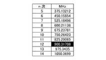
このときの、RFID用アンテナ部41の60次〜69次までの高次共振周波数は、図8に示すような特定の周波数に現れる。
Here, assuming that the
At this time, the high-order resonance frequencies from the 60th order to the 69th order of the
図8に示すように、64次及び68次の周波数は、上述したCDMAで使用する受信周波数帯「860〜870MHz」と送信周波数帯「915〜925MHz」にそれぞれ当ることになる。したがって、携帯電話装置1は、受信周波数帯「860〜870MHz」と送信周波数帯「915〜925MHz」でメインアンテナ部62を使って通信を行う場合に、共振用のコンデンサの容量を変更する。
As shown in FIG. 8, the 64th and 68th frequencies correspond to the reception frequency band “860 to 870 MHz” and the transmission frequency band “915 to 925 MHz” used in the above-described CDMA, respectively. Therefore, the
また、共振用のコンデンサの容量を変える場合、容量値をできるだけ小さくした方が、RFID用アンテナ部41の共振周波数が上がり、高次共振周波数の間隔が広くなるため、メインアンテナ部62の送受信に対する影響を避ける上で有利になる。
In addition, when changing the capacitance of the resonance capacitor, reducing the capacitance value as much as possible increases the resonance frequency of the
携帯電話装置1は、共振用のコンデンサRC1,RC2,RC3と、共振周波数調整用の回路RC4のそれぞれを分離部101で切り替えられる構成にしているため、共振用のコンデンサに可能な限り小さな容量(例えば、1pF)を設定しておけば、その容量まで共振用のコンデンサの容量を下げることができる。
Since the
例えば、共振用のコンデンサの容量を1.5pFにした場合には、RFID用アンテナ部41の共振周波数foは、75.026MHzになる。また、RFID用アンテナ部41の5次〜14次までの高次共振周波数は、図9に示す周波数になる。
For example, when the capacitance of the resonance capacitor is 1.5 pF, the resonance frequency fo of the
これより、受信周波数帯「860〜870MHz」と送信周波数帯「915〜925MHz」でメインアンテナ部62を使って通信を行う場合には、RFID用アンテナ部41の影響は無くなる。
Accordingly, when communication is performed using the
また、図9に示すように、携帯電話装置1は、受信周波数帯「843〜846MHz」と送信周波数帯「898〜901MHz」でメインアンテナ部62を使って通信を行う場合、RFID用アンテナ部41の12次の周波数が当ることになるので、共振用のコンデンサの容量を1pFに設定することで、RFID用アンテナ部41の影響を与えないようにすることができる(図10を参照)。
As shown in FIG. 9, when the
このようにして、携帯電話装置1は、メインアンテナ部62で通信する周波数帯によって、RFID用アンテナ部41の共振用コンデンサの容量を変化させるので、RFID用アンテナ部41の高次共振周波数の影響をメインアンテナ部62に与えないようにすることができる。
In this manner, the
また、携帯電話装置1は、RFID用アンテナ部41の共振周波数の変化(調整)を、メインアンテナ部62において通信を行う場合に使用される周波数帯に応じて行うので、メインアンテナ部62で通信を行わない場合には、RFID用アンテナ部41の共振周波数は変化(調整)せずにRFID用の共振周波数に合わせておいても良い。したがって、携帯電話装置1は、いつでもRFIDの機能が使用可能な状態にある。
In addition, since the
また、図11には、本実施例の方法によりRFID用アンテナ部41の共振周波数を調整した後において、500MHz〜2.5GHzの周波数によりVSWR(Voltage Standing Wave Ratio)を測定したときの結果を示し、また、図12には、RFID用アンテナ部41の共振周波数の調整前において、500MHz〜2.5GHzの周波数によりVSWRを測定したときの結果を示す。なお、測定においては、携帯電話装置1のメインアンテナ部62の給電点に測定装置(ネットワークアナライザ)を接続して行った。また、使用周波数帯の帯域幅がCDMAで使用する受信周波数帯と送信周波数帯をカバーする843MHz〜925MHz(図11及び図12中のA点〜B点)と、1.92GHz〜2.18GHz(図11及び図12中のC点〜D点)の携帯電話装置を使用して測定を行った。
Further, FIG. 11 shows a result when VSWR (Voltage Standing Wave Ratio) is measured at a frequency of 500 MHz to 2.5 GHz after adjusting the resonance frequency of the
図11及び図12から分かるように、RFID用アンテナ部41の共振周波数の調整前(図12)には、843MHz〜925MHz(図12中のA点〜B点)内にRFID用アンテナ部41の高次共振点の影響が現れているが(図12中のX)、RFID用アンテナ部41の共振周波数の調整後(図11)には、843MHz〜925MHz(図11中のA点〜B点)内にRFID用アンテナ部41の高次共振点の影響が消失している。
As can be seen from FIGS. 11 and 12, before the resonance frequency of the
したがって、携帯電話装置1は、本実施例の方法によりRFID用アンテナ部41のL値を変化させることで共振周波数を調整すると共に、当該調整後のRFID用アンテナ部41のL値を変化させることで、RFID用アンテナ部41の有する高次共振点の位置を、メインアンテナ部62で使用する周波数帯域からずらすことができるので、経年変化や落下等によってRFID用アンテナ部41の共振周波数f0にばらつきが生じた場合であっても、メインアンテナ部62への影響を低減することができ、メインアンテナ部62の利得劣化を低減することができる。
Therefore, the
また、携帯電話装置1は、上述したように、RFID用アンテナ部41の共振周波数f0を所定の周波数に調整することができるので、経年変化や落下等によってRFID用アンテナ部41の共振周波数f0にばらつきが生じ、感度が劣化した場合でも、いつでも工場出荷時の周波数に調整することができるので、良好な感度を維持することができる。
The
また、携帯電話装置1は、調整部53によりRFID用アンテナ部41の共振周波数を調整する際には、所定のスペック範囲内(RFID用アンテナ部41により通信が行える範囲内)で調整を行うことが好ましい。
In addition, when the
また、本実施例においては、RFID用アンテナ部41のターン数を切り替えることによって、RFID用アンテナ部41の共振周波数の調整を行うように説明したが、これに限られない。例えば、携帯電話装置1は、基準周波数(例えば、13.56MHz)を放射する基準周波数放射部を備えておき、当該基準周波数放射部により放射される信号をRFID用アンテナ部41で受信し、受信感度が最も良くなるように調整部53によりRFID用アンテナ部41の共振周波数を調整するような構成であっても良い。
Further, in this embodiment, the description has been made so that the resonance frequency of the
1 携帯電話装置
41 RFID用アンテナ部
51 RFID処理部
53 調整部
57、72 制御部
61 通信部
62 メインアンテナ部
71 処理部
101 分離部
102 信号発生部
103 検出部
104 操作検出部
DESCRIPTION OF
Claims (8)
前記筐体に配置され、第1使用周波数帯の信号を送受信する第1アンテナ部と、
前記筐体に配置され、前記第1使用周波数帯よりも高い周波数帯である第2使用周波数帯の信号を送受信する第2アンテナ部と、
前記第1アンテナ部の共振周波数を調整する調整部と、
前記第1使用周波数帯の信号の受信感度に基づいて前記第1アンテナ部のリアクタンス値を特定すると共に、前記特定されたリアクタンス値に基づいて前記第1アンテナ部の高次の共振周波数が前記第2使用周波数帯から離間するように前記調整部により前記第1アンテナ部の共振周波数を調整する制御部とを有し、
前記制御部は、前記第2アンテナ部により前記第2使用周波数帯の信号の受信を行ったときの受信感度が所定値を下回った場合、前記第1アンテナ部の高次の共振周波数が前記第2使用周波数帯から離間するように前記調整部により前記第1アンテナ部の共振周波数を調整する携帯電子機器。 A housing,
A first antenna unit disposed in the housing for transmitting and receiving signals in a first use frequency band;
A second antenna unit that is disposed in the housing and transmits / receives a signal in a second used frequency band that is a higher frequency band than the first used frequency band;
An adjustment unit for adjusting a resonance frequency of the first antenna unit;
The reactance value of the first antenna unit is specified based on the reception sensitivity of the signal in the first use frequency band, and the higher-order resonance frequency of the first antenna unit is determined based on the specified reactance value. by the adjusting unit so as to be separated from the 2 using the frequency band have a control unit to adjust the resonance frequency of the first antenna unit,
When the reception sensitivity when the signal of the second used frequency band is received by the second antenna unit is lower than a predetermined value, the control unit has a higher-order resonance frequency of the first antenna unit. 2. A portable electronic device that adjusts a resonance frequency of the first antenna unit by the adjusting unit so as to be separated from a use frequency band .
前記第1のループ部と前記第2のループ部の一方に接続され、当該接続された側のループ部から基準周波数の信号を発生させる信号発生部と、A signal generating unit connected to one of the first loop unit and the second loop unit, and generating a signal of a reference frequency from the connected loop unit;
前記第1のループ部と前記第2のループ部の他方に接続され、当該接続されたループ部の電気的特性を検出する検出部を備え、A detection unit connected to the other of the first loop unit and the second loop unit and detecting an electrical characteristic of the connected loop unit;
前記調整部は、前記第1のループ部と前記第2のループ部の他方に接続され、当該接続されたループ部の共振周波数を調整し、The adjustment unit is connected to the other of the first loop unit and the second loop unit, and adjusts the resonance frequency of the connected loop unit,
前記制御部は、前記分離部により、前記第1アンテナ部を前記第1のループ部と前記第2のループ部に分離すると共に、前記信号発生部により、前記第1のループ部と前記第2のループ部の一方から基準周波数の信号を発生し、かつ、前記検出部により、前記第1のループ部と前記第2のループ部の他方の電気的特性を検出し、さらに、前記調整部により、前記検出部の検出結果に応じて前記第1のループ部と前記第2のループ部の他方の共振周波数を調整する請求項1記載の携帯電子機器。The control unit separates the first antenna unit into the first loop unit and the second loop unit by the separation unit, and the first loop unit and the second loop by the signal generation unit. A reference frequency signal is generated from one of the loop sections, and the other electrical characteristics of the first loop section and the second loop section are detected by the detection section, and further, the adjustment section The portable electronic device according to claim 1, wherein the resonance frequency of the other of the first loop unit and the second loop unit is adjusted according to a detection result of the detection unit.
前記制御部は、前記操作検出部に対して所定の操作が行われると、前記分離部により、前記第1アンテナ部を前記第1のループ部と前記第2のループ部に分離すると共に、前記信号発生部により、前記第1のループ部と前記第2のループ部の一方から基準周波数の信号を発生し、かつ、前記検出部により、前記第1のループ部と前記第2のループ部の他方の電気的特性を検出し、さらに、前記調整部により、前記検出部の検出結果に応じて前記第1のループ部と前記第2のループ部の他方の共振周波数を調整する請求項2記載の携帯電子機器。When a predetermined operation is performed on the operation detection unit, the control unit separates the first antenna unit into the first loop unit and the second loop unit by the separation unit, and A signal generation unit generates a signal of a reference frequency from one of the first loop unit and the second loop unit, and the detection unit generates a signal of the first loop unit and the second loop unit. The other electrical characteristic is detected, and further, the resonance frequency of the other of the first loop portion and the second loop portion is adjusted by the adjustment unit according to a detection result of the detection unit. Portable electronic devices.
前記制御部は、前記分離部により、前記第1アンテナ部を前記第1のループ部と前記第2のループ部に分離すると共に、前記信号発生部により、前記第1のループ部と前記第2のループ部の両方から基準周波数の信号を発生し、かつ、前記検出部により、前記第1のループ部と前記第2のループ部の両方の電気的特性を検出し、その後、前記調整部により、前記検出部の検出結果に応じて前記第1のループ部と前記第2のループ部の両方の共振周波数を調整する請求項2乃至請求項4のいずれか一項に記載の携帯電子機器。 The control unit separates the first antenna unit into the first loop unit and the second loop unit by the separation unit, and the first loop unit and the second loop by the signal generation unit. The reference frequency signal is generated from both of the loop portions, and the electrical characteristics of both the first loop portion and the second loop portion are detected by the detection portion, and then the adjustment portion The portable electronic device according to claim 2, wherein the resonance frequencies of both the first loop unit and the second loop unit are adjusted according to a detection result of the detection unit.
前記制御部は、前記コンデンサの容量を調整することにより、前記第1アンテナ部の高次の共振周波数が前記第2使用周波数帯から離間するように前記調整部により前記第1アンテナ部の共振周波数を調整する請求項1乃至請求項7のいずれか一項に記載の携帯電子機器。The control unit adjusts the capacitance of the capacitor so that the higher-order resonance frequency of the first antenna unit is separated from the second use frequency band by the adjustment unit. The portable electronic device according to any one of claims 1 to 7, which adjusts the frequency.
Priority Applications (3)
| Application Number | Priority Date | Filing Date | Title |
|---|---|---|---|
| JP2010100978A JP5602484B2 (en) | 2010-04-26 | 2010-04-26 | Portable electronic devices |
| US13/094,405 US8816920B2 (en) | 2010-04-26 | 2011-04-26 | Mobile electronic device |
| KR1020110038899A KR101206617B1 (en) | 2010-04-26 | 2011-04-26 | Mobile electronic device |
Applications Claiming Priority (1)
| Application Number | Priority Date | Filing Date | Title |
|---|---|---|---|
| JP2010100978A JP5602484B2 (en) | 2010-04-26 | 2010-04-26 | Portable electronic devices |
Publications (3)
| Publication Number | Publication Date |
|---|---|
| JP2011234021A JP2011234021A (en) | 2011-11-17 |
| JP2011234021A5 JP2011234021A5 (en) | 2013-03-14 |
| JP5602484B2 true JP5602484B2 (en) | 2014-10-08 |
Family
ID=44815366
Family Applications (1)
| Application Number | Title | Priority Date | Filing Date |
|---|---|---|---|
| JP2010100978A Expired - Fee Related JP5602484B2 (en) | 2010-04-26 | 2010-04-26 | Portable electronic devices |
Country Status (3)
| Country | Link |
|---|---|
| US (1) | US8816920B2 (en) |
| JP (1) | JP5602484B2 (en) |
| KR (1) | KR101206617B1 (en) |
Families Citing this family (9)
| Publication number | Priority date | Publication date | Assignee | Title |
|---|---|---|---|---|
| JP5640655B2 (en) * | 2010-10-29 | 2014-12-17 | ソニー株式会社 | Portable communication device, reader / writer device, and resonance frequency adjusting method |
| FR2984020B1 (en) | 2011-12-13 | 2014-02-14 | Continental Automotive France | DEVICE AND METHOD FOR CONFIGURING ANTENNA |
| US9041617B2 (en) | 2011-12-20 | 2015-05-26 | Apple Inc. | Methods and apparatus for controlling tunable antenna systems |
| EP2669999B1 (en) * | 2012-05-31 | 2018-11-14 | Nxp B.V. | Adjustable antenna |
| TWI502817B (en) * | 2012-10-04 | 2015-10-01 | Acer Inc | Communication device |
| US20150115881A1 (en) * | 2013-10-25 | 2015-04-30 | Samsung Electro-Mechanics Co., Ltd. | Wireless power transceiver and portable terminal having the same |
| JP5839629B1 (en) * | 2014-07-18 | 2016-01-06 | デクセリアルズ株式会社 | Non-contact communication device, antenna circuit, antenna drive device, non-contact power supply device, tuning method, discovery method, and program for realizing these methods |
| JP6380441B2 (en) * | 2016-03-23 | 2018-08-29 | Smk株式会社 | Film with antenna and touch panel |
| US10186769B1 (en) * | 2017-07-20 | 2019-01-22 | Apple Inc. | Electronic device with shared control and power lines for antenna tuning circuits |
Family Cites Families (21)
| Publication number | Priority date | Publication date | Assignee | Title |
|---|---|---|---|---|
| JP3678167B2 (en) * | 2001-05-02 | 2005-08-03 | 株式会社村田製作所 | ANTENNA DEVICE AND RADIO COMMUNICATION DEVICE HAVING THE ANTENNA DEVICE |
| JP2004193875A (en) * | 2002-12-10 | 2004-07-08 | Murata Mfg Co Ltd | Antenna structure and communication apparatus provided with the same |
| JP2004227046A (en) | 2003-01-20 | 2004-08-12 | Hitachi Ltd | Portable information device |
| JP4181067B2 (en) * | 2003-09-18 | 2008-11-12 | Dxアンテナ株式会社 | Multi-frequency band antenna |
| JP2005150937A (en) * | 2003-11-12 | 2005-06-09 | Murata Mfg Co Ltd | Antenna structure and communication apparatus provided with the same |
| JP4466827B2 (en) * | 2003-12-11 | 2010-05-26 | 日本電気株式会社 | ANTENNA DEVICE AND WIRELESS COMMUNICATION DEVICE |
| KR101074240B1 (en) * | 2004-01-30 | 2011-10-14 | 가부시키가이샤 고쿠사이 덴키 츠신 기소 기주츠 겐큐쇼 | Receiver capable of receiving radio signal with high quality |
| JP4508190B2 (en) * | 2005-01-27 | 2010-07-21 | 株式会社村田製作所 | Antenna and wireless communication device |
| JP4951964B2 (en) * | 2005-12-28 | 2012-06-13 | 富士通株式会社 | Antenna and wireless communication device |
| WO2008007489A1 (en) * | 2006-07-13 | 2008-01-17 | Murata Manufacturing Co., Ltd. | Antenna device and wireless communication apparatus |
| EP2065975A1 (en) * | 2006-09-20 | 2009-06-03 | Murata Manufacturing Co. Ltd. | Antenna structure and wireless communication device employing the same |
| US20080081574A1 (en) * | 2006-09-28 | 2008-04-03 | Kai Shih | Embedded antenna |
| US8219143B2 (en) * | 2006-09-28 | 2012-07-10 | Kyocera Corporation | Mobile radio device |
| JP4752771B2 (en) * | 2007-01-19 | 2011-08-17 | 株式会社村田製作所 | Method for suppressing unwanted wave radiation of antenna structure, antenna structure, and radio communication apparatus including the same |
| JP4793701B2 (en) * | 2007-01-19 | 2011-10-12 | 株式会社村田製作所 | ANTENNA DEVICE AND RADIO COMMUNICATION DEVICE |
| WO2008120756A1 (en) * | 2007-03-29 | 2008-10-09 | Kyocera Corporation | Portable wireless device |
| WO2008120757A1 (en) * | 2007-03-29 | 2008-10-09 | Kyocera Corporation | Portable wireless device |
| JP5009361B2 (en) | 2007-03-29 | 2012-08-22 | 京セラ株式会社 | Portable radio |
| US8264412B2 (en) * | 2008-01-04 | 2012-09-11 | Apple Inc. | Antennas and antenna carrier structures for electronic devices |
| JP5150369B2 (en) * | 2008-05-28 | 2013-02-20 | 京セラ株式会社 | Communication equipment |
| WO2010110517A1 (en) * | 2009-03-23 | 2010-09-30 | Industry-University Cooperation Foundation Hanyang University | Antenna using a reactive element |
-
2010
- 2010-04-26 JP JP2010100978A patent/JP5602484B2/en not_active Expired - Fee Related
-
2011
- 2011-04-26 KR KR1020110038899A patent/KR101206617B1/en active IP Right Grant
- 2011-04-26 US US13/094,405 patent/US8816920B2/en not_active Expired - Fee Related
Also Published As
| Publication number | Publication date |
|---|---|
| KR20110119572A (en) | 2011-11-02 |
| JP2011234021A (en) | 2011-11-17 |
| US8816920B2 (en) | 2014-08-26 |
| US20110260940A1 (en) | 2011-10-27 |
| KR101206617B1 (en) | 2012-11-29 |
Similar Documents
| Publication | Publication Date | Title |
|---|---|---|
| JP5602484B2 (en) | Portable electronic devices | |
| JP5192385B2 (en) | Portable radio | |
| JP5681010B2 (en) | Portable electronic devices | |
| JP4466827B2 (en) | ANTENNA DEVICE AND WIRELESS COMMUNICATION DEVICE | |
| JP5009361B2 (en) | Portable radio | |
| JP4257349B2 (en) | Antenna device and wireless communication terminal | |
| US7589673B2 (en) | Antenna and mobile wireless equipment using the same | |
| JP5622612B2 (en) | Portable electronic devices | |
| JP5150369B2 (en) | Communication equipment | |
| JP2007060076A (en) | Mobile communication device | |
| JP5117607B2 (en) | Portable radio | |
| JP2009164772A (en) | Mobile phone | |
| JP4927162B2 (en) | Portable radio | |
| JP5468356B2 (en) | Mobile device | |
| WO2006043326A1 (en) | Sliding portable radio | |
| WO2004102822A1 (en) | Portable radio | |
| JP5448760B2 (en) | Mobile terminal and adjustment method | |
| JP5144419B2 (en) | Portable radio | |
| JP5289908B2 (en) | Communication equipment |
Legal Events
| Date | Code | Title | Description |
|---|---|---|---|
| RD04 | Notification of resignation of power of attorney |
Free format text: JAPANESE INTERMEDIATE CODE: A7424 Effective date: 20120803 |
|
| A521 | Request for written amendment filed |
Free format text: JAPANESE INTERMEDIATE CODE: A523 Effective date: 20130130 |
|
| A621 | Written request for application examination |
Free format text: JAPANESE INTERMEDIATE CODE: A621 Effective date: 20130215 |
|
| A977 | Report on retrieval |
Free format text: JAPANESE INTERMEDIATE CODE: A971007 Effective date: 20131225 |
|
| A131 | Notification of reasons for refusal |
Free format text: JAPANESE INTERMEDIATE CODE: A131 Effective date: 20140128 |
|
| A521 | Request for written amendment filed |
Free format text: JAPANESE INTERMEDIATE CODE: A523 Effective date: 20140324 |
|
| TRDD | Decision of grant or rejection written | ||
| A01 | Written decision to grant a patent or to grant a registration (utility model) |
Free format text: JAPANESE INTERMEDIATE CODE: A01 Effective date: 20140729 |
|
| A61 | First payment of annual fees (during grant procedure) |
Free format text: JAPANESE INTERMEDIATE CODE: A61 Effective date: 20140820 |
|
| R150 | Certificate of patent or registration of utility model |
Ref document number: 5602484 Country of ref document: JP Free format text: JAPANESE INTERMEDIATE CODE: R150 |
|
| LAPS | Cancellation because of no payment of annual fees |