EP2093811A2 - Package structure of compound semiconductor device and fabricating method thereof - Google Patents
Package structure of compound semiconductor device and fabricating method thereof Download PDFInfo
- Publication number
- EP2093811A2 EP2093811A2 EP09153073A EP09153073A EP2093811A2 EP 2093811 A2 EP2093811 A2 EP 2093811A2 EP 09153073 A EP09153073 A EP 09153073A EP 09153073 A EP09153073 A EP 09153073A EP 2093811 A2 EP2093811 A2 EP 2093811A2
- Authority
- EP
- European Patent Office
- Prior art keywords
- die
- conductive film
- bonding
- semiconductor device
- compound semiconductor
- Prior art date
- Legal status (The legal status is an assumption and is not a legal conclusion. Google has not performed a legal analysis and makes no representation as to the accuracy of the status listed.)
- Granted
Links
Images




Classifications
-
- H—ELECTRICITY
- H10—SEMICONDUCTOR DEVICES; ELECTRIC SOLID-STATE DEVICES NOT OTHERWISE PROVIDED FOR
- H10H—INORGANIC LIGHT-EMITTING SEMICONDUCTOR DEVICES HAVING POTENTIAL BARRIERS
- H10H20/00—Individual inorganic light-emitting semiconductor devices having potential barriers, e.g. light-emitting diodes [LED]
- H10H20/80—Constructional details
- H10H20/85—Packages
- H10H20/8506—Containers
-
- H—ELECTRICITY
- H10—SEMICONDUCTOR DEVICES; ELECTRIC SOLID-STATE DEVICES NOT OTHERWISE PROVIDED FOR
- H10F—INORGANIC SEMICONDUCTOR DEVICES SENSITIVE TO INFRARED RADIATION, LIGHT, ELECTROMAGNETIC RADIATION OF SHORTER WAVELENGTH OR CORPUSCULAR RADIATION
- H10F77/00—Constructional details of devices covered by this subclass
- H10F77/50—Encapsulations or containers
-
- H—ELECTRICITY
- H10—SEMICONDUCTOR DEVICES; ELECTRIC SOLID-STATE DEVICES NOT OTHERWISE PROVIDED FOR
- H10W—GENERIC PACKAGES, INTERCONNECTIONS, CONNECTORS OR OTHER CONSTRUCTIONAL DETAILS OF DEVICES COVERED BY CLASS H10
- H10W72/00—Interconnections or connectors in packages
- H10W72/50—Bond wires
- H10W72/551—Materials of bond wires
- H10W72/552—Materials of bond wires comprising metals or metalloids, e.g. silver
- H10W72/5522—Materials of bond wires comprising metals or metalloids, e.g. silver comprising gold [Au]
-
- H—ELECTRICITY
- H10—SEMICONDUCTOR DEVICES; ELECTRIC SOLID-STATE DEVICES NOT OTHERWISE PROVIDED FOR
- H10W—GENERIC PACKAGES, INTERCONNECTIONS, CONNECTORS OR OTHER CONSTRUCTIONAL DETAILS OF DEVICES COVERED BY CLASS H10
- H10W72/00—Interconnections or connectors in packages
- H10W72/851—Dispositions of multiple connectors or interconnections
- H10W72/874—On different surfaces
- H10W72/884—Die-attach connectors and bond wires
-
- H—ELECTRICITY
- H10—SEMICONDUCTOR DEVICES; ELECTRIC SOLID-STATE DEVICES NOT OTHERWISE PROVIDED FOR
- H10W—GENERIC PACKAGES, INTERCONNECTIONS, CONNECTORS OR OTHER CONSTRUCTIONAL DETAILS OF DEVICES COVERED BY CLASS H10
- H10W72/00—Interconnections or connectors in packages
- H10W72/90—Bond pads, in general
-
- H—ELECTRICITY
- H10—SEMICONDUCTOR DEVICES; ELECTRIC SOLID-STATE DEVICES NOT OTHERWISE PROVIDED FOR
- H10W—GENERIC PACKAGES, INTERCONNECTIONS, CONNECTORS OR OTHER CONSTRUCTIONAL DETAILS OF DEVICES COVERED BY CLASS H10
- H10W72/00—Interconnections or connectors in packages
- H10W72/90—Bond pads, in general
- H10W72/931—Shapes of bond pads
- H10W72/932—Plan-view shape, i.e. in top view
-
- H—ELECTRICITY
- H10—SEMICONDUCTOR DEVICES; ELECTRIC SOLID-STATE DEVICES NOT OTHERWISE PROVIDED FOR
- H10W—GENERIC PACKAGES, INTERCONNECTIONS, CONNECTORS OR OTHER CONSTRUCTIONAL DETAILS OF DEVICES COVERED BY CLASS H10
- H10W72/00—Interconnections or connectors in packages
- H10W72/90—Bond pads, in general
- H10W72/941—Dispositions of bond pads
- H10W72/9415—Dispositions of bond pads relative to the surface, e.g. recessed, protruding
-
- H—ELECTRICITY
- H10—SEMICONDUCTOR DEVICES; ELECTRIC SOLID-STATE DEVICES NOT OTHERWISE PROVIDED FOR
- H10W—GENERIC PACKAGES, INTERCONNECTIONS, CONNECTORS OR OTHER CONSTRUCTIONAL DETAILS OF DEVICES COVERED BY CLASS H10
- H10W74/00—Encapsulations, e.g. protective coatings
-
- H—ELECTRICITY
- H10—SEMICONDUCTOR DEVICES; ELECTRIC SOLID-STATE DEVICES NOT OTHERWISE PROVIDED FOR
- H10W—GENERIC PACKAGES, INTERCONNECTIONS, CONNECTORS OR OTHER CONSTRUCTIONAL DETAILS OF DEVICES COVERED BY CLASS H10
- H10W90/00—Package configurations
- H10W90/701—Package configurations characterised by the relative positions of pads or connectors relative to package parts
- H10W90/721—Package configurations characterised by the relative positions of pads or connectors relative to package parts of bump connectors
- H10W90/726—Package configurations characterised by the relative positions of pads or connectors relative to package parts of bump connectors between a chip and a stacked lead frame, conducting package substrate or heat sink
-
- H—ELECTRICITY
- H10—SEMICONDUCTOR DEVICES; ELECTRIC SOLID-STATE DEVICES NOT OTHERWISE PROVIDED FOR
- H10W—GENERIC PACKAGES, INTERCONNECTIONS, CONNECTORS OR OTHER CONSTRUCTIONAL DETAILS OF DEVICES COVERED BY CLASS H10
- H10W90/00—Package configurations
- H10W90/701—Package configurations characterised by the relative positions of pads or connectors relative to package parts
- H10W90/731—Package configurations characterised by the relative positions of pads or connectors relative to package parts of die-attach connectors
- H10W90/736—Package configurations characterised by the relative positions of pads or connectors relative to package parts of die-attach connectors between a chip and a stacked lead frame, conducting package substrate or heat sink
-
- H—ELECTRICITY
- H10—SEMICONDUCTOR DEVICES; ELECTRIC SOLID-STATE DEVICES NOT OTHERWISE PROVIDED FOR
- H10W—GENERIC PACKAGES, INTERCONNECTIONS, CONNECTORS OR OTHER CONSTRUCTIONAL DETAILS OF DEVICES COVERED BY CLASS H10
- H10W90/00—Package configurations
- H10W90/701—Package configurations characterised by the relative positions of pads or connectors relative to package parts
- H10W90/751—Package configurations characterised by the relative positions of pads or connectors relative to package parts of bond wires
- H10W90/756—Package configurations characterised by the relative positions of pads or connectors relative to package parts of bond wires between a chip and a stacked lead frame, conducting package substrate or heat sink
Definitions
- the present invention relates to a package structure of a compound semiconductor device and fabricating method thereof, and more particularly, to a thin package structure and fabricating method of a photoelectric semiconductor device.
- LED light emitting diode
- LCD liquid crystal display
- FIG. 1 is a schematic cross sectional diagram of the conventional SMD (surface mount device) of an LED device.
- An LED die 12 is mounted on an N-type conductive copper foil 13b covering an insulation layer 13c through die bonding paste 11, and is electrically connected to a P-type conductive copper foil 13a and the N-type conductive copper foil 13b through metal wires 15.
- the assembly of the P-type conductive copper foil 13a, N-type conductive copper foil 13b and insulation layer 13c is on a substrate 13.
- a transparent encapsulation material 14 covers the substrate 13, metal wires 15 and die 12 so that the whole LED device 10 can be protected against damage from environmental and external forces.
- the LED device 10 utilizes a common printed circuit board (PCB) as the substrate 13.
- PCB printed circuit board
- the total thickness of the LED device 10 is limited by the insulation layer 13c of the substrate 13, and thus cannot be reduced further.
- the insulation layer 13c is made mostly of epoxy resin with poor heat dissipation, and therefore is not suitable for a high power chemical compound semiconductor as a heat-transferring path.
- FIG. 2 is a schematic cross sectional diagram of a high integral package structure disclosed by U.S. Patent Publication No. 2004/0090756 .
- the package structure has an insulating layer coated on a temporary substrate, and has electrical circuits which have been previously designed and laid out on the insulating layer. Subsequently, LED dies 221 and 222 are adhered to a substrate 23, and the LED dies 221, 222 and the internal leads of the substrate 23 are connected to each other through metal wires 25 by the wire bonding (or through bumps by flip-chip bonding). Conventional epoxy resin covers the LED dies 221 and 222 by using a molding process. In order to reduce the thickness of the whole package, the temporary substrate is removed from the insulating layer by the illumination of laser light or UV light. Tin balls 26 are soldered to the default soldering pads. Thus, a highly integral and thinner package is obtained. However, the manufacturing processes of the package are complicated so that the cost of manufacture is high.
- the consumer electronics market is in urgent need of a photoelectric compound semiconductor device with a thin type package.
- the device not only needs to have a reduced thickness for saving space, but also needs to address the heat dissipation problem. With such a device, reliable, high power electronics products which can be more easily manufactured.
- One aspect of the present invention provides the package structure of a compound semiconductor device and fabricating method thereof.
- the semiconductor device has external electrodes or contacts uncovered by an encapsulation material. There is no printed circuit board between a die and external electrodes for transmitting electrical signals, so the heat dissipation of the device is improved.
- Another aspect of the present invention provides the package structure of a very thin semiconductor device and fabricating method thereof.
- the thickness of the device can be reduced for saving space due to the use of a thin substrate or a metallic film.
- the present invention discloses the package structure of a compound semiconductor device comprising a thin film substrate, a die and a transparent encapsulation material.
- the thin film substrate comprises a first conductive film, a second conductive film, and an insulating dielectric material.
- the die is mounted on the surface of the first conductive film.
- the transparent encapsulation material overlays the first conductive film, second conductive film, and die.
- the surfaces of the first conductive film and second conductive film which is opposite the transparent encapsulation material act as electrodes.
- the insulating dielectric material is between the first conductive film and the second conductive film.
- the thickness of the thin film substrate preferably ranges between 20-50 ⁇ m.
- the insulating dielectric material is SiO, SiN, SiON, TaO, AlO, TiO, AlN, TiN, epoxy resin, silicone or insulating polymer.
- the die is an LED die, a laser diode die or a photodiode die.
- the package structure of the compound semiconductor device further comprises at least one metal wire electrically connecting the die and thin film substrate.
- the first conductive film further comprises a first wire-bonding groove for bonding the metal wire
- the second conductive film further comprises a second wire-bonding groove for bonding the metal wire.
- the package structure of the compound semiconductor device further comprises a plurality of bumps electrically connecting the die and thin film substrate.
- the first conductive film further comprises a die-bonding groove on which the die is mounted.
- a reflecting layer is overlaid on the surfaces of the die-bonding groove.
- the package structure of the compound semiconductor device further comprises a patterned insulating material layer stacked on the thin film substrate.
- the insulating material layer comprises a die-bonding groove for bonding the die and a wire-bonding groove for bonding the metal wire.
- the present invention discloses the manufacturing method of the package structure of a compound semiconductor device comprising the steps of: providing a thin film substrate comprising a first conductive film, a second conductive film, and an insulating dielectric material; mounting a die onto the first conductive film, electrically connecting an anode of the die to the first conductive film, electrically connecting a cathode of the die to the second conductive film; and overlaying a transparent encapsulation material on the die.
- the thin film substrate is manufactured by the following steps: providing a sheet; forming at least one slot to divide the sheet into the first conductive film and second conductive film, and filling the insulating dielectric material in the slot.
- the slot is formed by a drilling process, an etching process or a punching process.
- the manufacturing method further comprises a step of forming a die-bonding groove on the first conductive film.
- the manufacturing method further comprises a step of forming a plurality of wire-bonding grooves on the first conductive film and second conductive film, wherein each of the wire-bonding grooves is formed where at least one of the metal wires is bonded.
- the manufacturing method further comprises a step of stacking a patterned insulating material layer on the thin film substrate, wherein the insulating material layer comprises a die-bonding groove for bonding the die and a plurality of wire-bonding grooves for bonding at least one metal wire.
- the step of mounting the die onto the thin film substrate further electrically connects the die to the thin film substrate by wire bonding or flip-chip bonding.
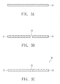
- FIGS. 3A-3C are schematic illustrations showing the manufacturing steps of a thin film substrate in accordance with the present invention.
- a sheet 34 with a thickness of between 20-50 ⁇ m is provided; for instance copper foil or a metal film with superior conductivity.
- a slot 33 is formed on the sheet 34 by a drilling process, an etching process or a punching process.
- the slot 33 separates a first conductive film 31 at one side from a second conductive film 32 at another side, that is, they are electrically isolated from each other, as shown in FIG. 3B .
- an insulating dielectric material 35 is filled in the slot 33 so that the manufacture of a thin film substrate 30 is finished.
- the insulating dielectric material 35 can be SiO, SiN, SiON, TaO, AlO, TiO, AlN, TiN, epoxy resin, silicone or polymer.
- the electrical insulation between the first conductive film 31 and second conductive film 32 is improved, and the thin film substrate 30 is more rigid, as shown in FIG. 3C .
- FIG. 4A is a cross-sectional diagram of the package structure of a compound semiconductor device in accordance with the present invention.
- a compound semiconductor device 40 utilizes the die-bonding technology to adhere a compound semiconductor die 43 to the first conductive film 31 of the thin film substrate 30, that is, the die 43 is mounted on the surface of the first conductive film 31 by a die-bonding adhesive 47.
- the die 43 can be an LED die, a laser diode die or a photodiode die.
- the die 43 and thin film substrate 30 are electrically connected to each other through metal wires 44 so that the thin film substrate 30 acts as the package carrier of the die 43 and metal wires 44.
- a transparent encapsulation material 46 overlays the die 43, metal wires 44, and thin film substrate 30 in order to provide anti-moisture and protection effects.
- the transparent encapsulation material 46 can be epoxy resin or silicone.
- FIG. 4B is a top view of the compound semiconductor device in FIG. 4A .
- a portion of the transparent encapsulation material 46 is removed.
- Two metal wires 44 respectively go from the surface of the die 43 toward the first conductive film 31 and the second conductive film 32, and connect them.
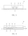
- FIG. 5 is a cross-sectional diagram of the package structure of a compound semiconductor device in accordance with another embodiment of the present invention.
- the compound semiconductor device 50 utilizes a flip-chip bonding process to mount the die 43 on the thin film substrate 30 through bumps 54.
- the active surface of the die 43 faces the thin film substrate 30, and tin balls are utilized to connect the bonding pads of the die 43 and thin film substrate 30 to form the bumps 54.
- the bumps 54 are melted due to solder flux after a reflow process, and solidify to electrically connect them.
- a transparent encapsulation material 46 overlays the die 43, metal wires 44, and thin film substrate 30 in order to have anti-moisture and protection effects.
- there are several advantages such as short current paths and excellent heat dissipation.
- the present invention can reduce the loop height of the metal wires.
- FIG. 6 is a cross-sectional diagram of the package structure of a compound semiconductor device in accordance with another embodiment of the present invention.
- the thickness of the package structure is further reduced and the illumination brightness of the device is increased.
- a die-bonding groove 411 is formed on the first conductive film 31' of the thin film substrate 30a, and a reflecting layer 412 is deposited on the sidewalls and bottom of the die-bonding groove 411.
- the die-bonding groove 411 can be formed by a photolithography etching process, an electroforming process and a drilling process.
- the die 43 is adhered to the bottom of the die-bonding groove 411, and the die-bonding groove 411 acts as a cup-like reflective cavity.
- the brightness of the compound semiconductor device 60 is improved.
- another advantage is that when the die 43 is placed in the die-bonding groove 411 and the metal wires 44 electrically connect the die 44 and thin film substrate 30a, the height of the wire loop of the gold wires is significantly reduced so as to further reduce the thickness of the entire package structure.
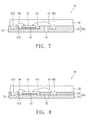
- FIG. 7 is a cross-sectional diagram of the package structure of a compound semiconductor device in accordance with another embodiment of the present invention. Compared with the previous embodiment, this embodiment further reduces the thickness of the package structure.
- a wire-bonding groove 413 is formed on the first conductive film 31'' of the thin film substrate 30b for one of the metal wires 44 to indicate the melting location of a second bond.
- a wire-bonding groove 421 is formed on the second conductive film 32' for another of the metal wires 44 to indicate the melting location of a second bond. Because the second bond of the metal wire 44 is descended to the wire-bonding groove, the thickness of the package structure of the compound semiconductor device 60 is reduced.
- the die-bonding groove and wire-bonding groove are formed by a photolithography etching process, an electroforming process and a drilling process. Furthermore, a patterned insulating material layer 36 can be formed on the thin film substrate 30, and a die-bonding groove 411 and wire-bonding grooves 413 and 421 are formed on the insulating material layer 36, as shown in FIG. 8 . Therefore, the thickness of the package structure of the compound semiconductor device 80 is reduced, which can prevent the metal wire 44 connected to the second conductive film 32 from short-circuit resulting from improperly contacting the first conductive film 31.
- FIGS. 9A-9D are schematic illustrations showing the formation of a die-bonding groove or a wire-bonding groove by an electroforming process.
- a patterned insulating material layer 36' such as a photoresist material is formed on the thin film substrate 30.
- a metal layer 37 is gradually grown on the surfaces of the first conductive film 31 and the second conductive film 32 uncovered by the insulating material layer 36' by an electroforming process.
- the insulating material layer 36' is removed (for example, a photoresist striping step) to expose the die-bonding groove 411 and wire-bonding grooves 413 and 421.
- a package structure of a compound semiconductor device comprising a thin film substrate, a die, at least one metal wire and a transparent encapsulation material.
- the thin film substrate comprises a first conductive film, a second conductive film, and an insulating dielectric material.
- the die is mounted on the surface of the first conductive film, and is electrically connected to the first conductive film and the second conductive film through the metal wire.
- the transparent encapsulation material overlays the first conductive film, second conductive film, and die.
- the surfaces of the first conductive film and second conductive film which is opposite the transparent encapsulation material act as electrodes.
- the insulating dielectric material is between the first conductive film and second conductive film.
Landscapes
- Led Device Packages (AREA)
- Structures Or Materials For Encapsulating Or Coating Semiconductor Devices Or Solid State Devices (AREA)
Abstract
Description
- The present invention relates to a package structure of a compound semiconductor device and fabricating method thereof, and more particularly, to a thin package structure and fabricating method of a photoelectric semiconductor device.
- Because the light emitting diode (LED) pertaining to the photoelectric device has advantages of a small body, high efficiency and long life, it is expected to be an excellent illumination source into the next generation. In addition, LCD (liquid crystal display) technology is developing rapidly and full color is the current trend in electronic product displays. Therefore, white series LEDs are not only applicable to indication lights and large size display screens but also to most consumer electronic products such as mobile phones and personal digital assistants (PDA).
-
FIG. 1 is a schematic cross sectional diagram of the conventional SMD (surface mount device) of an LED device. AnLED die 12 is mounted on an N-typeconductive copper foil 13b covering aninsulation layer 13c through diebonding paste 11, and is electrically connected to a P-typeconductive copper foil 13a and the N-typeconductive copper foil 13b throughmetal wires 15. The assembly of the P-typeconductive copper foil 13a, N-typeconductive copper foil 13b andinsulation layer 13c is on asubstrate 13. Furthermore, atransparent encapsulation material 14 covers thesubstrate 13,metal wires 15 and die 12 so that thewhole LED device 10 can be protected against damage from environmental and external forces. - The
LED device 10 utilizes a common printed circuit board (PCB) as thesubstrate 13. The total thickness of theLED device 10 is limited by theinsulation layer 13c of thesubstrate 13, and thus cannot be reduced further. However, the current trend of consumer electronic products is toward lightweight, small packages. Accordingly, each of the internal devices of the consumer electronics product and its shell needs to be miniaturized. On the other hand, theinsulation layer 13c is made mostly of epoxy resin with poor heat dissipation, and therefore is not suitable for a high power chemical compound semiconductor as a heat-transferring path. -
FIG. 2 is a schematic cross sectional diagram of a high integral package structure disclosed byU.S. Patent Publication No. 2004/0090756 . The package structure has an insulating layer coated on a temporary substrate, and has electrical circuits which have been previously designed and laid out on the insulating layer. Subsequently, LED dies 221 and 222 are adhered to a substrate 23, and the LED dies 221, 222 and the internal leads of the substrate 23 are connected to each other throughmetal wires 25 by the wire bonding (or through bumps by flip-chip bonding). Conventional epoxy resin covers theLED dies Tin balls 26 are soldered to the default soldering pads. Thus, a highly integral and thinner package is obtained. However, the manufacturing processes of the package are complicated so that the cost of manufacture is high. - In view of the above, the consumer electronics market is in urgent need of a photoelectric compound semiconductor device with a thin type package. The device not only needs to have a reduced thickness for saving space, but also needs to address the heat dissipation problem. With such a device, reliable, high power electronics products which can be more easily manufactured.
- One aspect of the present invention provides the package structure of a compound semiconductor device and fabricating method thereof. The semiconductor device has external electrodes or contacts uncovered by an encapsulation material. There is no printed circuit board between a die and external electrodes for transmitting electrical signals, so the heat dissipation of the device is improved.
- Another aspect of the present invention provides the package structure of a very thin semiconductor device and fabricating method thereof. The thickness of the device can be reduced for saving space due to the use of a thin substrate or a metallic film.
- According the aforesaid aspects, the present invention discloses the package structure of a compound semiconductor device comprising a thin film substrate, a die and a transparent encapsulation material. The thin film substrate comprises a first conductive film, a second conductive film, and an insulating dielectric material. The die is mounted on the surface of the first conductive film. The transparent encapsulation material overlays the first conductive film, second conductive film, and die. The surfaces of the first conductive film and second conductive film which is opposite the transparent encapsulation material act as electrodes. The insulating dielectric material is between the first conductive film and the second conductive film.
- The thickness of the thin film substrate preferably ranges between 20-50µm.
- The insulating dielectric material is SiO, SiN, SiON, TaO, AlO, TiO, AlN, TiN, epoxy resin, silicone or insulating polymer.
- The die is an LED die, a laser diode die or a photodiode die.
- The package structure of the compound semiconductor device further comprises at least one metal wire electrically connecting the die and thin film substrate. The first conductive film further comprises a first wire-bonding groove for bonding the metal wire, and the second conductive film further comprises a second wire-bonding groove for bonding the metal wire.
- The package structure of the compound semiconductor device further comprises a plurality of bumps electrically connecting the die and thin film substrate.
- The first conductive film further comprises a die-bonding groove on which the die is mounted. A reflecting layer is overlaid on the surfaces of the die-bonding groove.
- The package structure of the compound semiconductor device further comprises a patterned insulating material layer stacked on the thin film substrate. The insulating material layer comprises a die-bonding groove for bonding the die and a wire-bonding groove for bonding the metal wire.
- The present invention discloses the manufacturing method of the package structure of a compound semiconductor device comprising the steps of: providing a thin film substrate comprising a first conductive film, a second conductive film, and an insulating dielectric material; mounting a die onto the first conductive film, electrically connecting an anode of the die to the first conductive film, electrically connecting a cathode of the die to the second conductive film; and overlaying a transparent encapsulation material on the die.
- The thin film substrate is manufactured by the following steps: providing a sheet; forming at least one slot to divide the sheet into the first conductive film and second conductive film, and filling the insulating dielectric material in the slot.
- The slot is formed by a drilling process, an etching process or a punching process.
- The manufacturing method further comprises a step of forming a die-bonding groove on the first conductive film.
- The manufacturing method further comprises a step of forming a plurality of wire-bonding grooves on the first conductive film and second conductive film, wherein each of the wire-bonding grooves is formed where at least one of the metal wires is bonded.
- The manufacturing method further comprises a step of stacking a patterned insulating material layer on the thin film substrate, wherein the insulating material layer comprises a die-bonding groove for bonding the die and a plurality of wire-bonding grooves for bonding at least one metal wire.
- The step of mounting the die onto the thin film substrate further electrically connects the die to the thin film substrate by wire bonding or flip-chip bonding.
- The objectives and advantages of the present invention will become apparent upon reading the following description and upon reference to the accompanying drawings in which:
- FIG. 1
- is a schematic cross sectional diagram of the conventional SMD (surface mount device) of an LED device;
- FIG. 2
- is a schematic cross sectional diagram of a highly integral package structure disclosed by
U.S. Patent Publication No. 2004/0090756 ; - FIGS. 3A-3C
- are schematic illustrations showing the manufacturing steps of a thin film substrate in accordance with the present invention;
- FIG. 4A
- is a cross-sectional diagram of the package structure of a compound semiconductor device in accordance with the present invention;
- FIG. 4B
- is a top view of the compound semiconductor device in
FIG. 4A ; - FIG. 5
- is a cross-sectional diagram of the package structure of a compound semiconductor device in accordance with another embodiment of the present invention;
- FIG. 6
- is a cross-sectional diagram of the package structure of a compound semiconductor device in accordance with another embodiment of the present invention;
- FIG. 7
- is a cross-sectional diagram of the package structure of a compound semiconductor device in accordance with another embodiment of the present invention;
- FIG. 8
- is a cross-sectional diagram of the package structure of a compound semiconductor device in accordance with another embodiment of the present invention; and
- FIGS. 9A-9D
- are schematic illustrations showing the formation of a die-bonding groove or a wire-bonding groove by an electroforming process.
-
FIGS. 3A-3C are schematic illustrations showing the manufacturing steps of a thin film substrate in accordance with the present invention. As shown inFIG. 3A , asheet 34 with a thickness of between 20-50µm is provided; for instance copper foil or a metal film with superior conductivity. Moreover, aslot 33 is formed on thesheet 34 by a drilling process, an etching process or a punching process. Theslot 33 separates a firstconductive film 31 at one side from a secondconductive film 32 at another side, that is, they are electrically isolated from each other, as shown inFIG. 3B . Subsequently, an insulatingdielectric material 35 is filled in theslot 33 so that the manufacture of athin film substrate 30 is finished. The insulatingdielectric material 35 can be SiO, SiN, SiON, TaO, AlO, TiO, AlN, TiN, epoxy resin, silicone or polymer. In this regard, the electrical insulation between the firstconductive film 31 and secondconductive film 32 is improved, and thethin film substrate 30 is more rigid, as shown inFIG. 3C . -
FIG. 4A is a cross-sectional diagram of the package structure of a compound semiconductor device in accordance with the present invention. Acompound semiconductor device 40 utilizes the die-bonding technology to adhere a compound semiconductor die 43 to the firstconductive film 31 of thethin film substrate 30, that is, thedie 43 is mounted on the surface of the firstconductive film 31 by a die-bonding adhesive 47. The die 43 can be an LED die, a laser diode die or a photodiode die. Moreover, thedie 43 andthin film substrate 30 are electrically connected to each other throughmetal wires 44 so that thethin film substrate 30 acts as the package carrier of thedie 43 andmetal wires 44. Final, by a molding process, atransparent encapsulation material 46 overlays thedie 43,metal wires 44, andthin film substrate 30 in order to provide anti-moisture and protection effects. Thetransparent encapsulation material 46 can be epoxy resin or silicone. -
FIG. 4B is a top view of the compound semiconductor device inFIG. 4A . For clearly illustrating the connection between the die 43,metal wires 44, andthin film substrate 30, a portion of thetransparent encapsulation material 46 is removed. Twometal wires 44 respectively go from the surface of the die 43 toward the firstconductive film 31 and the secondconductive film 32, and connect them. -
FIG. 5 is a cross-sectional diagram of the package structure of a compound semiconductor device in accordance with another embodiment of the present invention. Thecompound semiconductor device 50 utilizes a flip-chip bonding process to mount the die 43 on thethin film substrate 30 throughbumps 54. Compared withFIG. 4A , the active surface of the die 43 faces thethin film substrate 30, and tin balls are utilized to connect the bonding pads of thedie 43 andthin film substrate 30 to form thebumps 54. Thebumps 54 are melted due to solder flux after a reflow process, and solidify to electrically connect them. Final, by a molding process, atransparent encapsulation material 46 overlays thedie 43,metal wires 44, andthin film substrate 30 in order to have anti-moisture and protection effects. In this embodiment, there are several advantages such as short current paths and excellent heat dissipation. In addition, compared with the previous embodiment, the present invention can reduce the loop height of the metal wires. -
FIG. 6 is a cross-sectional diagram of the package structure of a compound semiconductor device in accordance with another embodiment of the present invention. Regarding this embodiment, the thickness of the package structure is further reduced and the illumination brightness of the device is increased. A die-bonding groove 411 is formed on the first conductive film 31' of the thin film substrate 30a, and a reflectinglayer 412 is deposited on the sidewalls and bottom of the die-bonding groove 411. The die-bonding groove 411 can be formed by a photolithography etching process, an electroforming process and a drilling process. Thedie 43 is adhered to the bottom of the die-bonding groove 411, and the die-bonding groove 411 acts as a cup-like reflective cavity. Lateral light emitted from the die 43 can be effectively reflected by the reflectinglayer 412, and redirected towards the upper side. Therefore, the brightness of thecompound semiconductor device 60 is improved. In this embodiment, another advantage is that when thedie 43 is placed in the die-bonding groove 411 and themetal wires 44 electrically connect thedie 44 and thin film substrate 30a, the height of the wire loop of the gold wires is significantly reduced so as to further reduce the thickness of the entire package structure. -
FIG. 7 is a cross-sectional diagram of the package structure of a compound semiconductor device in accordance with another embodiment of the present invention. Compared with the previous embodiment, this embodiment further reduces the thickness of the package structure. A wire-bonding groove 413 is formed on the first conductive film 31'' of thethin film substrate 30b for one of themetal wires 44 to indicate the melting location of a second bond. Similarly, a wire-bonding groove 421 is formed on the second conductive film 32' for another of themetal wires 44 to indicate the melting location of a second bond. Because the second bond of themetal wire 44 is descended to the wire-bonding groove, the thickness of the package structure of thecompound semiconductor device 60 is reduced. - In the above embodiments, the die-bonding groove and wire-bonding groove are formed by a photolithography etching process, an electroforming process and a drilling process. Furthermore, a patterned insulating
material layer 36 can be formed on thethin film substrate 30, and a die-bonding groove 411 and wire-bonding grooves material layer 36, as shown inFIG. 8 . Therefore, the thickness of the package structure of thecompound semiconductor device 80 is reduced, which can prevent themetal wire 44 connected to the secondconductive film 32 from short-circuit resulting from improperly contacting the firstconductive film 31. -
FIGS. 9A-9D are schematic illustrations showing the formation of a die-bonding groove or a wire-bonding groove by an electroforming process. A patterned insulating material layer 36' such as a photoresist material is formed on thethin film substrate 30. Ametal layer 37 is gradually grown on the surfaces of the firstconductive film 31 and the secondconductive film 32 uncovered by the insulating material layer 36' by an electroforming process. Moreover, the insulating material layer 36' is removed (for example, a photoresist striping step) to expose the die-bonding groove 411 and wire-bonding grooves - In summary there is disclosed a package structure of a compound semiconductor device comprising a thin film substrate, a die, at least one metal wire and a transparent encapsulation material. The thin film substrate comprises a first conductive film, a second conductive film, and an insulating dielectric material. The die is mounted on the surface of the first conductive film, and is electrically connected to the first conductive film and the second conductive film through the metal wire. The transparent encapsulation material overlays the first conductive film, second conductive film, and die. The surfaces of the first conductive film and second conductive film which is opposite the transparent encapsulation material act as electrodes. The insulating dielectric material is between the first conductive film and second conductive film.
- The above-described embodiments of the present invention are intended to be illustrative only. Those skilled in the art may devise numerous alternative embodiments without departing from the scope of the following claims.
Claims (15)
- A package structure of a compound semiconductor device, comprising:a thin film substrate including a first conductive film, a second conductive film, and an insulating dielectric material, wherein the insulating dielectric material is between the first conductive film and the second conductive film;a die mounted on a surface of the first conductive film; anda transparent encapsulation material overlaying the first conductive film, the second conductive film, and the die.
- The package structure of the compound semiconductor device of Claim 1, wherein the thickness of the thin film substrate ranges between 20-50µm.
- The package structure of the compound semiconductor device of Claim 1 or 2, wherein the material of the insulating dielectric material is SiO, SiN, SiON, TaO, AlO, TiO, AlN, TiN, epoxy resin, silicone or insulating polymer.
- The package structure of a compound semiconductor device of one of the preceding Claims, wherein the die is an LED, a laser LED or a photodiode die.
- The package structure of a compound semiconductor device of one of the preceding Claims, further comprising:at least one metal wire electrically connecting the die and the thin film substrate, and/ora plurality of bumps electrically connecting the die and the thin film substrate.
- The package structure of a compound semiconductor device of one of the preceding Claims, wherein the first conductive film further comprises a die-bonding groove on which the die is mounted.
- The package structure of a compound semiconductor device of Claim 6, further comprising a reflecting layer overlaid on the die-bonding groove.
- The package structure of a compound semiconductor device of Claim 5, wherein the first conductive film further comprises a first wire-bonding groove for bonding the metal wire, and the second conductive film further comprises a second wire-bonding groove for bonding the metal wire.
- The package structure of a compound semiconductor device of one of the preceding Claims, further comprising:a patterned insulating material layer stacked on the thin film substrate, wherein the insulating material layer comprises a die-bonding groove for bonding the die, and/or a patterned insulating material layer stacked on the thin film substrate, wherein the insulating material layer comprises a die-bonding groove for bonding the die and at least one wire-bonding groove for bonding the metal wire.
- A manufacturing method of a package structure of a compound semiconductor device, comprising the steps of:providing a thin film substrate comprising a first conductive film, a second conductive film, and an insulating dielectric material;mounting a die onto the first conductive film, electrically connecting an anode of the die to the first conductive film, and electrically connecting a cathode of the die to the second conductive film; andoverlaying a transparent encapsulation material on the die.
- The manufacturing method of a package structure of a compound semiconductor device of Claim 10,
wherein thin film substrate is manufactured by the following steps:providing a sheet;forming at least one slot on the sheet to divide the sheet into the first conductive film and the second conductive film; andfilling the insulating dielectric material in the slot. - The manufacturing method of a package structure of a compound semiconductor device of Claim 11,
wherein the slot is formed by a drilling process, an etching process or a punching process; and/or the method is further comprising a step of forming a die-bonding groove on the first conductive film; and/or the method is further comprising a step of stacking a patterned insulating material layer on the thin film substrate, wherein the insulating material layer comprises a die-bonding groove for bonding the die and a plurality of wire-bonding grooves for bonding at least one metal wire. - The manufacturing method of a package structure of a compound semiconductor device of Claim 12,
wherein the die is mounted onto the die-bonding groove; and/or the method is further comprising a step of forming a plurality of wire-bonding grooves on the first conductive film and the second conductive film, wherein each of the wire-bonding grooves is formed where at least one of the metal wires is bonded. - The manufacturing method of a package structure of a compound semiconductor device of Claim 10, wherein the step of mounting the die onto the first conductive film further comprises a sub-step of electrically connecting the die to the thin film substrate by wire bonding or flip-chip bonding.
- The manufacturing method of a package structure of a compound semiconductor device of Claim 14, wherein the wire-bonding grooves are formed by a photolithography etching process, an electroforming process and a drilling process.
Applications Claiming Priority (1)
| Application Number | Priority Date | Filing Date | Title |
|---|---|---|---|
| TW097105846A TW200937667A (en) | 2008-02-20 | 2008-02-20 | Package structure of chemical compound semiconductor device and fabricating method thereof |
Publications (3)
| Publication Number | Publication Date |
|---|---|
| EP2093811A2 true EP2093811A2 (en) | 2009-08-26 |
| EP2093811A3 EP2093811A3 (en) | 2013-05-29 |
| EP2093811B1 EP2093811B1 (en) | 2017-01-11 |
Family
ID=40433921
Family Applications (1)
| Application Number | Title | Priority Date | Filing Date |
|---|---|---|---|
| EP09153073.3A Not-in-force EP2093811B1 (en) | 2008-02-20 | 2009-02-18 | Package structure of compound semiconductor device |
Country Status (3)
| Country | Link |
|---|---|
| US (2) | US7893528B2 (en) |
| EP (1) | EP2093811B1 (en) |
| TW (1) | TW200937667A (en) |
Cited By (1)
| Publication number | Priority date | Publication date | Assignee | Title |
|---|---|---|---|---|
| US8502257B2 (en) | 2009-11-05 | 2013-08-06 | Visera Technologies Company Limited | Light-emitting diode package |
Families Citing this family (16)
| Publication number | Priority date | Publication date | Assignee | Title |
|---|---|---|---|---|
| TWI398933B (en) * | 2008-03-05 | 2013-06-11 | 榮創能源科技股份有限公司 | Package structure of integrated circuit component and manufacturing method thereof |
| KR20110018777A (en) * | 2009-08-18 | 2011-02-24 | 삼성엘이디 주식회사 | Light emitting diode package |
| TW201131708A (en) * | 2010-03-08 | 2011-09-16 | Harvatek Corp | LED package structure for increasing heat-dissipating efficiency and method of manufacturing the same |
| US8598612B2 (en) * | 2010-03-30 | 2013-12-03 | Micron Technology, Inc. | Light emitting diode thermally enhanced cavity package and method of manufacture |
| TWI472067B (en) * | 2010-04-28 | 2015-02-01 | Lg伊諾特股份有限公司 | Optical package and method of manufacturing same |
| KR101114719B1 (en) | 2010-08-09 | 2012-02-29 | 엘지이노텍 주식회사 | Light emitting device and lighting system having same |
| KR101114197B1 (en) * | 2010-08-09 | 2012-02-22 | 엘지이노텍 주식회사 | Light emitting device and lighting system having same |
| TWI533483B (en) * | 2010-08-09 | 2016-05-11 | Lg伊諾特股份有限公司 | Illuminating device |
| TWI425680B (en) * | 2010-10-29 | 2014-02-01 | Advanced Optoelectronic Tech | Light emitting diode package |
| TWI424591B (en) * | 2011-08-23 | 2014-01-21 | Jentech Prec Ind Co Ltd | Led package structure and manufacturing method thereof |
| CN103022011B (en) * | 2011-09-23 | 2015-10-07 | 讯芯电子科技(中山)有限公司 | Semiconductor package and manufacture method thereof |
| JP5885499B2 (en) * | 2011-12-27 | 2016-03-15 | 株式会社ディスコ | Tool cutting method |
| KR20150031849A (en) * | 2013-09-17 | 2015-03-25 | (주)포인트엔지니어링 | Substrate for mounting a chip and chip package |
| EP3818298B1 (en) | 2018-07-03 | 2024-10-23 | Glowgadget, LLC | Flexible lighting panel and lighting fixture |
| JP7450466B2 (en) | 2020-06-22 | 2024-03-15 | スタンレー電気株式会社 | Light-emitting device and method for manufacturing the light-emitting device |
| CN120417582B (en) * | 2025-07-02 | 2025-09-09 | 上海芯龙半导体技术股份有限公司 | Photoelectric device packaging structure and manufacturing method thereof |
Citations (1)
| Publication number | Priority date | Publication date | Assignee | Title |
|---|---|---|---|---|
| US20040090756A1 (en) | 2002-11-07 | 2004-05-13 | Kwun-Yo Ho | Chip packaging structure and manufacturing process thereof |
Family Cites Families (13)
| Publication number | Priority date | Publication date | Assignee | Title |
|---|---|---|---|---|
| JP4215306B2 (en) | 1998-08-27 | 2009-01-28 | シチズン電子株式会社 | Semiconductor package and manufacturing method thereof |
| JP3945037B2 (en) * | 1998-09-04 | 2007-07-18 | 松下電器産業株式会社 | Photoelectric conversion element and manufacturing method thereof |
| JP2002232018A (en) * | 2000-11-28 | 2002-08-16 | Nippon Telegr & Teleph Corp <Ntt> | Method for producing ultraviolet light source, ultraviolet light source component, and method for producing optical device |
| DE10228634A1 (en) * | 2002-06-26 | 2004-01-22 | Osram Opto Semiconductors Gmbh | Surface-mountable miniature luminescence and / or photo diode and process for their production |
| JP2005535144A (en) * | 2002-07-31 | 2005-11-17 | オスラム オプト セミコンダクターズ ゲゼルシャフト ミット ベシュレンクテル ハフツング | Surface-mountable semiconductor device and method for manufacturing the semiconductor device |
| JP3910171B2 (en) | 2003-02-18 | 2007-04-25 | シャープ株式会社 | Semiconductor light emitting device, method for manufacturing the same, and electronic imaging device |
| US7276782B2 (en) | 2003-10-31 | 2007-10-02 | Harvatek Corporation | Package structure for semiconductor |
| DE10353679A1 (en) * | 2003-11-17 | 2005-06-02 | Siemens Ag | Cost-effective, miniaturized assembly and connection technology for LEDs and other optoelectronic modules |
| US7183588B2 (en) * | 2004-01-08 | 2007-02-27 | Avago Technologies Ecbu Ip (Singapore) Pte. Ltd. | Light emission device |
| JP4608294B2 (en) | 2004-11-30 | 2011-01-12 | 日亜化学工業株式会社 | RESIN MOLDED BODY, SURFACE MOUNTED LIGHT EMITTING DEVICE AND METHOD FOR PRODUCING THEM |
| US20060131708A1 (en) * | 2004-12-16 | 2006-06-22 | Ng Kee Y | Packaged electronic devices, and method for making same |
| US7301225B2 (en) * | 2006-02-28 | 2007-11-27 | Freescale Semiconductor, Inc. | Multi-row lead frame |
| US20090026470A1 (en) * | 2007-07-23 | 2009-01-29 | Novalite Optronics Corp. | Super thin side-view light-emitting diode (led) package and fabrication method thereof |
-
2008
- 2008-02-20 TW TW097105846A patent/TW200937667A/en unknown
-
2009
- 2009-02-13 US US12/370,923 patent/US7893528B2/en active Active - Reinstated
- 2009-02-18 EP EP09153073.3A patent/EP2093811B1/en not_active Not-in-force
-
2010
- 2010-08-13 US US12/856,052 patent/US8298861B2/en not_active Expired - Fee Related
Patent Citations (1)
| Publication number | Priority date | Publication date | Assignee | Title |
|---|---|---|---|---|
| US20040090756A1 (en) | 2002-11-07 | 2004-05-13 | Kwun-Yo Ho | Chip packaging structure and manufacturing process thereof |
Cited By (1)
| Publication number | Priority date | Publication date | Assignee | Title |
|---|---|---|---|---|
| US8502257B2 (en) | 2009-11-05 | 2013-08-06 | Visera Technologies Company Limited | Light-emitting diode package |
Also Published As
| Publication number | Publication date |
|---|---|
| US8298861B2 (en) | 2012-10-30 |
| EP2093811A3 (en) | 2013-05-29 |
| TW200937667A (en) | 2009-09-01 |
| US20100304535A1 (en) | 2010-12-02 |
| US7893528B2 (en) | 2011-02-22 |
| EP2093811B1 (en) | 2017-01-11 |
| US20090206358A1 (en) | 2009-08-20 |
Similar Documents
| Publication | Publication Date | Title |
|---|---|---|
| EP2093811B1 (en) | Package structure of compound semiconductor device | |
| EP2897182B1 (en) | Light emitting device | |
| US20090022198A1 (en) | Package structure of compound semiconductor device and fabricating method thereof | |
| JP6131048B2 (en) | LED module | |
| US8344406B2 (en) | Light emitting diode package and manufacturing method thereof | |
| JP2005322937A (en) | Semiconductor light emitting device with flexible substrate | |
| US9425373B2 (en) | Light emitting module | |
| US20100096746A1 (en) | Package module structure of compound semiconductor devices and fabricating method thereof | |
| US8017964B2 (en) | Light emitting device | |
| US20120056223A1 (en) | Led package structure and packaging method thereof | |
| US20070290307A1 (en) | Light emitting diode module | |
| CN102160197A (en) | Photoelectric component packaging base | |
| CN101630668A (en) | Encapsulation structure of compound semiconductor element and photoelectric element and manufacturing method thereof | |
| JP2012109521A (en) | Led module device and manufacturing method thereof | |
| CN101728370B (en) | Encapsulation modular structure of compound semiconductor elements and manufacturing method thereof | |
| CN101546737B (en) | Package structure of compound semiconductor component and manufacturing method thereof | |
| KR101363980B1 (en) | Optical module and manufacturing method thereof | |
| JP2012165016A (en) | Light-emitting device | |
| TWI393273B (en) | Method for manufacturing light emitting diode assembly | |
| KR101129002B1 (en) | Optical package and manufacturing method of the same | |
| JP2007005722A (en) | Envelope for optical semiconductor element and optical semiconductor device using the same | |
| US12040434B2 (en) | Diode package structure and manufacturing method thereof | |
| JP5861356B2 (en) | Lead frame with reflecting member for optical semiconductor device, lead frame for optical semiconductor device, lead frame substrate for optical semiconductor device, optical semiconductor device, method for manufacturing lead frame with reflecting member for optical semiconductor device, and optical semiconductor device Production method | |
| TW201025676A (en) | Compound semiconductor device package module structure and fabricating method thereof | |
| KR101146659B1 (en) | Optical package and manufacturing method of the same |
Legal Events
| Date | Code | Title | Description |
|---|---|---|---|
| PUAI | Public reference made under article 153(3) epc to a published international application that has entered the european phase |
Free format text: ORIGINAL CODE: 0009012 |
|
| AK | Designated contracting states |
Kind code of ref document: A2 Designated state(s): AT BE BG CH CY CZ DE DK EE ES FI FR GB GR HR HU IE IS IT LI LT LU LV MC MK MT NL NO PL PT RO SE SI SK TR |
|
| AX | Request for extension of the european patent |
Extension state: AL BA RS |
|
| PUAL | Search report despatched |
Free format text: ORIGINAL CODE: 0009013 |
|
| AK | Designated contracting states |
Kind code of ref document: A3 Designated state(s): AT BE BG CH CY CZ DE DK EE ES FI FR GB GR HR HU IE IS IT LI LT LU LV MC MK MT NL NO PL PT RO SE SI SK TR |
|
| AX | Request for extension of the european patent |
Extension state: AL BA RS |
|
| RIC1 | Information provided on ipc code assigned before grant |
Ipc: H01L 31/0203 20060101AFI20130424BHEP Ipc: H01L 33/48 20100101ALI20130424BHEP |
|
| 17P | Request for examination filed |
Effective date: 20131129 |
|
| RBV | Designated contracting states (corrected) |
Designated state(s): AT BE BG CH CY CZ DE DK EE ES FI FR GB GR HR HU IE IS IT LI LT LU LV MC MK MT NL NO PL PT RO SE SI SK TR |
|
| RBV | Designated contracting states (corrected) |
Designated state(s): AT BE BG CH CY CZ DE DK EE ES FI FR GB GR HR HU IE IS IT LI LT LU LV MC MK MT NL NO PL PT RO SE SI SK TR |
|
| AKX | Designation fees paid |
Designated state(s): AT BE BG CH CY CZ DE DK EE ES FI FR GB GR HR HU IE IS IT LI LT LU LV MC MK MT NL NO PL PT RO SE SI SK TR |
|
| 17Q | First examination report despatched |
Effective date: 20160428 |
|
| REG | Reference to a national code |
Ref country code: DE Ref legal event code: R079 Ref document number: 602009043642 Country of ref document: DE Free format text: PREVIOUS MAIN CLASS: H01L0033000000 Ipc: H01L0031020300 |
|
| GRAP | Despatch of communication of intention to grant a patent |
Free format text: ORIGINAL CODE: EPIDOSNIGR1 |
|
| RIC1 | Information provided on ipc code assigned before grant |
Ipc: H01L 33/62 20100101ALI20160829BHEP Ipc: H01L 31/0203 20060101AFI20160829BHEP Ipc: H01L 33/48 20100101ALI20160829BHEP |
|
| INTG | Intention to grant announced |
Effective date: 20161005 |
|
| GRAS | Grant fee paid |
Free format text: ORIGINAL CODE: EPIDOSNIGR3 |
|
| GRAA | (expected) grant |
Free format text: ORIGINAL CODE: 0009210 |
|
| AK | Designated contracting states |
Kind code of ref document: B1 Designated state(s): AT BE BG CH CY CZ DE DK EE ES FI FR GB GR HR HU IE IS IT LI LT LU LV MC MK MT NL NO PL PT RO SE SI SK TR |
|
| REG | Reference to a national code |
Ref country code: GB Ref legal event code: FG4D |
|
| REG | Reference to a national code |
Ref country code: CH Ref legal event code: EP |
|
| REG | Reference to a national code |
Ref country code: AT Ref legal event code: REF Ref document number: 861977 Country of ref document: AT Kind code of ref document: T Effective date: 20170115 |
|
| REG | Reference to a national code |
Ref country code: IE Ref legal event code: FG4D |
|
| REG | Reference to a national code |
Ref country code: FR Ref legal event code: PLFP Year of fee payment: 9 |
|
| REG | Reference to a national code |
Ref country code: DE Ref legal event code: R096 Ref document number: 602009043642 Country of ref document: DE |
|
| REG | Reference to a national code |
Ref country code: LT Ref legal event code: MG4D |
|
| REG | Reference to a national code |
Ref country code: NL Ref legal event code: MP Effective date: 20170111 |
|
| PG25 | Lapsed in a contracting state [announced via postgrant information from national office to epo] |
Ref country code: BE Free format text: LAPSE BECAUSE OF NON-PAYMENT OF DUE FEES Effective date: 20170228 |
|
| REG | Reference to a national code |
Ref country code: AT Ref legal event code: MK05 Ref document number: 861977 Country of ref document: AT Kind code of ref document: T Effective date: 20170111 |
|
| PG25 | Lapsed in a contracting state [announced via postgrant information from national office to epo] |
Ref country code: NL Free format text: LAPSE BECAUSE OF FAILURE TO SUBMIT A TRANSLATION OF THE DESCRIPTION OR TO PAY THE FEE WITHIN THE PRESCRIBED TIME-LIMIT Effective date: 20170111 |
|
| PG25 | Lapsed in a contracting state [announced via postgrant information from national office to epo] |
Ref country code: IS Free format text: LAPSE BECAUSE OF FAILURE TO SUBMIT A TRANSLATION OF THE DESCRIPTION OR TO PAY THE FEE WITHIN THE PRESCRIBED TIME-LIMIT Effective date: 20170511 Ref country code: GR Free format text: LAPSE BECAUSE OF FAILURE TO SUBMIT A TRANSLATION OF THE DESCRIPTION OR TO PAY THE FEE WITHIN THE PRESCRIBED TIME-LIMIT Effective date: 20170412 Ref country code: NO Free format text: LAPSE BECAUSE OF FAILURE TO SUBMIT A TRANSLATION OF THE DESCRIPTION OR TO PAY THE FEE WITHIN THE PRESCRIBED TIME-LIMIT Effective date: 20170411 Ref country code: HR Free format text: LAPSE BECAUSE OF FAILURE TO SUBMIT A TRANSLATION OF THE DESCRIPTION OR TO PAY THE FEE WITHIN THE PRESCRIBED TIME-LIMIT Effective date: 20170111 Ref country code: FI Free format text: LAPSE BECAUSE OF FAILURE TO SUBMIT A TRANSLATION OF THE DESCRIPTION OR TO PAY THE FEE WITHIN THE PRESCRIBED TIME-LIMIT Effective date: 20170111 Ref country code: LT Free format text: LAPSE BECAUSE OF FAILURE TO SUBMIT A TRANSLATION OF THE DESCRIPTION OR TO PAY THE FEE WITHIN THE PRESCRIBED TIME-LIMIT Effective date: 20170111 |
|
| PG25 | Lapsed in a contracting state [announced via postgrant information from national office to epo] |
Ref country code: PT Free format text: LAPSE BECAUSE OF FAILURE TO SUBMIT A TRANSLATION OF THE DESCRIPTION OR TO PAY THE FEE WITHIN THE PRESCRIBED TIME-LIMIT Effective date: 20170511 Ref country code: ES Free format text: LAPSE BECAUSE OF FAILURE TO SUBMIT A TRANSLATION OF THE DESCRIPTION OR TO PAY THE FEE WITHIN THE PRESCRIBED TIME-LIMIT Effective date: 20170111 Ref country code: SE Free format text: LAPSE BECAUSE OF FAILURE TO SUBMIT A TRANSLATION OF THE DESCRIPTION OR TO PAY THE FEE WITHIN THE PRESCRIBED TIME-LIMIT Effective date: 20170111 Ref country code: LV Free format text: LAPSE BECAUSE OF FAILURE TO SUBMIT A TRANSLATION OF THE DESCRIPTION OR TO PAY THE FEE WITHIN THE PRESCRIBED TIME-LIMIT Effective date: 20170111 Ref country code: AT Free format text: LAPSE BECAUSE OF FAILURE TO SUBMIT A TRANSLATION OF THE DESCRIPTION OR TO PAY THE FEE WITHIN THE PRESCRIBED TIME-LIMIT Effective date: 20170111 Ref country code: PL Free format text: LAPSE BECAUSE OF FAILURE TO SUBMIT A TRANSLATION OF THE DESCRIPTION OR TO PAY THE FEE WITHIN THE PRESCRIBED TIME-LIMIT Effective date: 20170111 Ref country code: BG Free format text: LAPSE BECAUSE OF FAILURE TO SUBMIT A TRANSLATION OF THE DESCRIPTION OR TO PAY THE FEE WITHIN THE PRESCRIBED TIME-LIMIT Effective date: 20170411 |
|
| REG | Reference to a national code |
Ref country code: CH Ref legal event code: PL |
|
| REG | Reference to a national code |
Ref country code: DE Ref legal event code: R097 Ref document number: 602009043642 Country of ref document: DE |
|
| PG25 | Lapsed in a contracting state [announced via postgrant information from national office to epo] |
Ref country code: SK Free format text: LAPSE BECAUSE OF FAILURE TO SUBMIT A TRANSLATION OF THE DESCRIPTION OR TO PAY THE FEE WITHIN THE PRESCRIBED TIME-LIMIT Effective date: 20170111 Ref country code: CZ Free format text: LAPSE BECAUSE OF FAILURE TO SUBMIT A TRANSLATION OF THE DESCRIPTION OR TO PAY THE FEE WITHIN THE PRESCRIBED TIME-LIMIT Effective date: 20170111 Ref country code: EE Free format text: LAPSE BECAUSE OF FAILURE TO SUBMIT A TRANSLATION OF THE DESCRIPTION OR TO PAY THE FEE WITHIN THE PRESCRIBED TIME-LIMIT Effective date: 20170111 Ref country code: RO Free format text: LAPSE BECAUSE OF FAILURE TO SUBMIT A TRANSLATION OF THE DESCRIPTION OR TO PAY THE FEE WITHIN THE PRESCRIBED TIME-LIMIT Effective date: 20170111 Ref country code: CH Free format text: LAPSE BECAUSE OF NON-PAYMENT OF DUE FEES Effective date: 20170228 Ref country code: LI Free format text: LAPSE BECAUSE OF NON-PAYMENT OF DUE FEES Effective date: 20170228 Ref country code: IT Free format text: LAPSE BECAUSE OF FAILURE TO SUBMIT A TRANSLATION OF THE DESCRIPTION OR TO PAY THE FEE WITHIN THE PRESCRIBED TIME-LIMIT Effective date: 20170111 |
|
| PLBE | No opposition filed within time limit |
Free format text: ORIGINAL CODE: 0009261 |
|
| STAA | Information on the status of an ep patent application or granted ep patent |
Free format text: STATUS: NO OPPOSITION FILED WITHIN TIME LIMIT |
|
| REG | Reference to a national code |
Ref country code: IE Ref legal event code: MM4A |
|
| PG25 | Lapsed in a contracting state [announced via postgrant information from national office to epo] |
Ref country code: MC Free format text: LAPSE BECAUSE OF FAILURE TO SUBMIT A TRANSLATION OF THE DESCRIPTION OR TO PAY THE FEE WITHIN THE PRESCRIBED TIME-LIMIT Effective date: 20170111 Ref country code: DK Free format text: LAPSE BECAUSE OF FAILURE TO SUBMIT A TRANSLATION OF THE DESCRIPTION OR TO PAY THE FEE WITHIN THE PRESCRIBED TIME-LIMIT Effective date: 20170111 |
|
| 26N | No opposition filed |
Effective date: 20171012 |
|
| GBPC | Gb: european patent ceased through non-payment of renewal fee |
Effective date: 20170411 |
|
| PG25 | Lapsed in a contracting state [announced via postgrant information from national office to epo] |
Ref country code: LU Free format text: LAPSE BECAUSE OF NON-PAYMENT OF DUE FEES Effective date: 20170218 |
|
| REG | Reference to a national code |
Ref country code: FR Ref legal event code: PLFP Year of fee payment: 10 |
|
| REG | Reference to a national code |
Ref country code: BE Ref legal event code: MM Effective date: 20170228 |
|
| PG25 | Lapsed in a contracting state [announced via postgrant information from national office to epo] |
Ref country code: GB Free format text: LAPSE BECAUSE OF NON-PAYMENT OF DUE FEES Effective date: 20170411 Ref country code: SI Free format text: LAPSE BECAUSE OF FAILURE TO SUBMIT A TRANSLATION OF THE DESCRIPTION OR TO PAY THE FEE WITHIN THE PRESCRIBED TIME-LIMIT Effective date: 20170111 Ref country code: IE Free format text: LAPSE BECAUSE OF NON-PAYMENT OF DUE FEES Effective date: 20170218 |
|
| PG25 | Lapsed in a contracting state [announced via postgrant information from national office to epo] |
Ref country code: MT Free format text: LAPSE BECAUSE OF NON-PAYMENT OF DUE FEES Effective date: 20170218 |
|
| PG25 | Lapsed in a contracting state [announced via postgrant information from national office to epo] |
Ref country code: HU Free format text: LAPSE BECAUSE OF FAILURE TO SUBMIT A TRANSLATION OF THE DESCRIPTION OR TO PAY THE FEE WITHIN THE PRESCRIBED TIME-LIMIT; INVALID AB INITIO Effective date: 20090218 |
|
| PG25 | Lapsed in a contracting state [announced via postgrant information from national office to epo] |
Ref country code: CY Free format text: LAPSE BECAUSE OF NON-PAYMENT OF DUE FEES Effective date: 20170111 |
|
| PG25 | Lapsed in a contracting state [announced via postgrant information from national office to epo] |
Ref country code: MK Free format text: LAPSE BECAUSE OF FAILURE TO SUBMIT A TRANSLATION OF THE DESCRIPTION OR TO PAY THE FEE WITHIN THE PRESCRIBED TIME-LIMIT Effective date: 20170111 |
|
| REG | Reference to a national code |
Ref country code: DE Ref legal event code: R082 Ref document number: 602009043642 Country of ref document: DE |
|
| PG25 | Lapsed in a contracting state [announced via postgrant information from national office to epo] |
Ref country code: TR Free format text: LAPSE BECAUSE OF FAILURE TO SUBMIT A TRANSLATION OF THE DESCRIPTION OR TO PAY THE FEE WITHIN THE PRESCRIBED TIME-LIMIT Effective date: 20170111 |
|
| PGFP | Annual fee paid to national office [announced via postgrant information from national office to epo] |
Ref country code: DE Payment date: 20200204 Year of fee payment: 12 |
|
| PGFP | Annual fee paid to national office [announced via postgrant information from national office to epo] |
Ref country code: FR Payment date: 20200127 Year of fee payment: 12 |
|
| REG | Reference to a national code |
Ref country code: DE Ref legal event code: R119 Ref document number: 602009043642 Country of ref document: DE |
|
| PG25 | Lapsed in a contracting state [announced via postgrant information from national office to epo] |
Ref country code: FR Free format text: LAPSE BECAUSE OF NON-PAYMENT OF DUE FEES Effective date: 20210228 Ref country code: DE Free format text: LAPSE BECAUSE OF NON-PAYMENT OF DUE FEES Effective date: 20210901 |