EP2089968B2 - Control method and circuit for power semiconductor devices - Google Patents
Control method and circuit for power semiconductor devices Download PDFInfo
- Publication number
- EP2089968B2 EP2089968B2 EP07804437.7A EP07804437A EP2089968B2 EP 2089968 B2 EP2089968 B2 EP 2089968B2 EP 07804437 A EP07804437 A EP 07804437A EP 2089968 B2 EP2089968 B2 EP 2089968B2
- Authority
- EP
- European Patent Office
- Prior art keywords
- voltage
- power semiconductor
- switching device
- semiconductor switching
- diode
- Prior art date
- Legal status (The legal status is an assumption and is not a legal conclusion. Google has not performed a legal analysis and makes no representation as to the accuracy of the status listed.)
- Not-in-force
Links
- 239000004065 semiconductor Substances 0.000 title claims abstract description 81
- 238000000034 method Methods 0.000 title claims abstract description 49
- 230000008859 change Effects 0.000 claims abstract description 50
- 230000002441 reversible effect Effects 0.000 claims abstract description 15
- 230000008569 process Effects 0.000 claims description 8
- 238000012544 monitoring process Methods 0.000 claims description 7
- 230000003247 decreasing effect Effects 0.000 claims description 6
- 230000001360 synchronised effect Effects 0.000 claims description 5
- 230000033228 biological regulation Effects 0.000 claims description 4
- 230000001419 dependent effect Effects 0.000 claims description 2
- 238000001514 detection method Methods 0.000 claims 2
- 230000001105 regulatory effect Effects 0.000 abstract description 4
- 238000011084 recovery Methods 0.000 description 6
- 230000003750 conditioning effect Effects 0.000 description 5
- 230000001276 controlling effect Effects 0.000 description 5
- 230000007423 decrease Effects 0.000 description 5
- 238000010586 diagram Methods 0.000 description 3
- 230000001939 inductive effect Effects 0.000 description 3
- 238000013459 approach Methods 0.000 description 2
- 230000006399 behavior Effects 0.000 description 2
- 230000003111 delayed effect Effects 0.000 description 2
- 230000003993 interaction Effects 0.000 description 2
- 230000009467 reduction Effects 0.000 description 2
- 230000001052 transient effect Effects 0.000 description 2
- 230000003044 adaptive effect Effects 0.000 description 1
- 230000008901 benefit Effects 0.000 description 1
- 230000005540 biological transmission Effects 0.000 description 1
- 230000000903 blocking effect Effects 0.000 description 1
- 239000003990 capacitor Substances 0.000 description 1
- 238000007796 conventional method Methods 0.000 description 1
- 230000005669 field effect Effects 0.000 description 1
- 230000003137 locomotive effect Effects 0.000 description 1
- 229910044991 metal oxide Inorganic materials 0.000 description 1
- 150000004706 metal oxides Chemical class 0.000 description 1
- 238000012986 modification Methods 0.000 description 1
- 230000004048 modification Effects 0.000 description 1
- 230000003287 optical effect Effects 0.000 description 1
- 238000005457 optimization Methods 0.000 description 1
- 230000010355 oscillation Effects 0.000 description 1
- 230000003071 parasitic effect Effects 0.000 description 1
- 230000004044 response Effects 0.000 description 1
- 238000004088 simulation Methods 0.000 description 1
Images



Classifications
-
- H—ELECTRICITY
- H03—ELECTRONIC CIRCUITRY
- H03K—PULSE TECHNIQUE
- H03K17/00—Electronic switching or gating, i.e. not by contact-making and –breaking
- H03K17/16—Modifications for eliminating interference voltages or currents
- H03K17/168—Modifications for eliminating interference voltages or currents in composite switches
-
- H—ELECTRICITY
- H03—ELECTRONIC CIRCUITRY
- H03K—PULSE TECHNIQUE
- H03K17/00—Electronic switching or gating, i.e. not by contact-making and –breaking
- H03K17/08—Modifications for protecting switching circuit against overcurrent or overvoltage
- H03K17/081—Modifications for protecting switching circuit against overcurrent or overvoltage without feedback from the output circuit to the control circuit
- H03K17/0814—Modifications for protecting switching circuit against overcurrent or overvoltage without feedback from the output circuit to the control circuit by measures taken in the output circuit
- H03K17/08148—Modifications for protecting switching circuit against overcurrent or overvoltage without feedback from the output circuit to the control circuit by measures taken in the output circuit in composite switches
-
- H—ELECTRICITY
- H03—ELECTRONIC CIRCUITRY
- H03K—PULSE TECHNIQUE
- H03K17/00—Electronic switching or gating, i.e. not by contact-making and –breaking
- H03K17/08—Modifications for protecting switching circuit against overcurrent or overvoltage
- H03K17/082—Modifications for protecting switching circuit against overcurrent or overvoltage by feedback from the output to the control circuit
- H03K17/0828—Modifications for protecting switching circuit against overcurrent or overvoltage by feedback from the output to the control circuit in composite switches
-
- H—ELECTRICITY
- H03—ELECTRONIC CIRCUITRY
- H03K—PULSE TECHNIQUE
- H03K17/00—Electronic switching or gating, i.e. not by contact-making and –breaking
- H03K17/16—Modifications for eliminating interference voltages or currents
- H03K17/161—Modifications for eliminating interference voltages or currents in field-effect transistor switches
- H03K17/165—Modifications for eliminating interference voltages or currents in field-effect transistor switches by feedback from the output circuit to the control circuit
- H03K17/166—Soft switching
Definitions
- This invention generally relates to the control of power semiconductor devices, and in embodiments particularly relates to the concurrent control of power semiconductor switching devices and freewheel diodes.
- Power semiconductor devices are widely in use for a large range of power applications, from low voltage chips, computers, locomotives, to high voltage transmission lines.
- freewheel diodes need to be used in relation with the power semiconductor switching devices such as IGBTs (insulated gate bipolar transistors) or MOSFETs (metal oxide semiconductor field effect transistors) for a continuous load current conduction to avoid large voltage damaging the semiconductor devices and the circuit.
- High power IGBTs are often supplied as a module with diodes that act as freewheel diodes within the module. IGBTs are typically found in parallel with the diodes. Reliable switching operation of both a power semiconductor switching device and a freewheel diodes is of primary importance.
- Granted European patent application EP0508171 B1 (Siemens Aktiengesellschaft, Niedermeier Ernst, published 14.10.1992) relates to a switched-mode power output stage for inductive loads with a freewheeling circuit, in which both the rate of voltage change at the junction between load and switching device and the rate of change of the load current flowing through the switching device are attempted to be adjusted, the latter independently of the rate of voltage change.
- a voltage proportional to the load current and a voltage proportional to the drain voltage are in each case differentiated and the signals thus obtained are superimposed on the control clock signal for the switching device.
- a first method is of controlling the commutation of a power semiconductor switching device and freewheel diode pair, the method comprising the stages of: applying, upon receipt of a switch-on command signal, a voltage function to a control terminal or the gate of the power semiconductor switching device, said voltage function allowing regulation of a current rise in the device whilst changing the voltage across the device; and substantially at the instant when the voltage across the diode (V AK ) begins to change from an on-state towards an off-state voltage, applying a voltage function to the control terminal or the gate of the power semiconductor switching device to enable the voltage change across the power semiconductor switching device to substantially track the voltage change across the diode.
- the voltage function that is the voltage shape or waveform, is in embodiments chosen to control the rate of change of the current and may comprise, a (slow) ramp or a (small) step, for example of around 10 per cent of the total change.
- a (slow) ramp or a (small) step for example of around 10 per cent of the total change.
- parasitic or other inductance in the circuit more particularly in the series connected switching device and diode, results in a gradual change of current.
- voltage feedback is employed to control the switching an approximately linear ramp of current may be achieved.
- the concept is to change the voltage on the control terminal or gate of the active switching device using an initial ramp or step to determine when the passive switching device (diode) begins to switch.
- the switching of the diode can be controlled by the active switch, thus enabling the switching of the active (IGBT) and passive (diode) switches to be synchronised.
- embodiments of the method involve watching the diode to determine when it begins to switch; this point can be identified by identifying when the voltage across the diode begins to fall towards or through zero.
- One can define a sign convention such that when the diode is on the diode voltage is called positive and when the voltage begins to fall below zero and becomes negative the diode turns off- that is when the voltage across the diode reverses.
- the voltages across the active and passive switching devices operate as a see-saw, so that as one rises the other falls, and vice versa.
- changing the voltage across the power semiconductor switching device comprises maintaining a falling voltage, at a pre-determined rate, across the device.
- changing the voltage across this device may comprise maintaining the voltage to follow a predetermined waveform which may be stepped or linear (or piecewise linear) or both.
- the method comprises synchronising the start of a voltage appearing across the freewheel diode (when the voltage across the diode begins to fall towards or through zero) with the main voltage fall of the power semiconductor switching device (that is when the diode begins switching) and a current peak in the power semiconductor switching device.
- V AK diode voltage
- the peak in I C is where the rate of change of current changes from positive to negative and thus is a conveniently identifiable feature on the diode current waveform. However it can be seen that this is not precisely coincident with the switching point of the diode although it is substantially at this instant (in embodiments we are slightly late).
- the voltage function used to control the rate of voltage decrease across the power semiconductor switching device is determined by closed loop feedback monitoring.
- the voltage function for controlling the power semiconductor switching device to track the diode voltage falling can be altered to ensure an optimum commutation process. That is in embodiments the voltage function (waveform) may be controlled to control the commutation process.
- a circuit for implementing a method as described above comprises: a gate drive circuit for providing a gate drive voltage for the power semiconductor switching device, and a control signal generating circuit, connected to the gate drive circuit, wherein upon receipt of a switch-on signal a first stage control signal is produced to control the gate drive circuit to drive the power semiconductor switching device to change said voltage across said device and a second stage control signal is generated, synchronised with the start of said voltage across said diode falling, to control the gate drive circuit to drive the voltage across the power semiconductor switching device to change substantially in synchronism with the diode voltage.
- the voltages across the diode and across the power semiconductor switching device operate as a see-saw, that is the changes in voltage across these device substantially track one another. (If absolute voltage polarities are employed this may be expressed as both voltages falling at substantially the same rate).
- control signal generating circuit comprises a closed loop voltage feedback circuit to feedback a sensed voltage from the power semiconductor switching device and freewheel diode pair to the control signal generating circuit, and a current monitoring circuit to feedback a current sense signal from the device and diode pair to the control signal generating circuit.
- first and second stage control signals are responsive to the sensed voltage and sensed current signal.
- sensed current signal senses a rate of change of the current through the device and diode pair.
- a still further related arrangement is a commutation control circuit for a chopper, said chopper comprising an active switching device and a passive switching device coupled in series, said commutation control circuit being configured to control commutation of said switching devices such that said switching devices switch substantially in synchronism, said control circuit comprising; a first sense input to receive a first sense signal from said chopper circuit; a second sense input to receive a second sense signal from said chopper circuit; and a control signal generating circuit coupled to said first and second sense inputs and having an output to control switching of said active switching device; and wherein said control signal generating circuit is configured to use said first and second sense signals to determine when said passive switch begins to switch and to control said active switching device such that said active and passive switching devices switch substantially in synchronism.
- the commutation control circuit identifies a feature in a current sense signal sensing a current through the passive switching device, for example the polarity change of the rate change of diode current (or, in more accurately synchronised embodiments, the zero crossing of the diode voltage), to determine when the passive switch begins to switch.
- the other sense signal comprises a voltage sense signal. In principle two voltage sense signals could be employed but this is less preferable because it is likely that for many applications one of the sensed voltages would be a relatively high voltage.
- control signal generating circuit comprises at least one digital control loop. For example a rate of change of current may be sensed and used to generate a (1 bit) timing control signal when the di / dt changes from positive to negative (or vice versa). This may be used to identify, approximately, a corner in the diode voltage, identifying a point at which the diode commences to switch.
- the control signal generating circuit may then generate a control signal to change the voltage on the active switch, for example the collector or emitter voltage of an IGBT, to bring this voltage down rapidly. In embodiments this may be performed by using digital circuitry to control a digital-to-analogue converter in response to the timing control signal.
- This function may be performed, for example, by high speed digital circuitry and implemented in an FPGA (field programmable gate array). Often switching times are of order nanoseconds and such an arrangement facilitates control on this timescale. Such arrangements facilitate control of the switching active and passive devices in synchronism.
- FPGA field programmable gate array
- the method comprises the stages of: applying, upon receipt of a switch-on command signal, a voltage function to the control terminal or the gate of the power semiconductor switching device that allows a regulated current rise in the device whilst maintaining the voltage across the device falling at a predetermined rate; and at substantially the instant when the voltage across the diode begins to change from the on-state towards the off-state level, applying a voltage function to the control terminal or the gate of the power semiconductor switching device to enable the voltage falling across the power semiconductor switching device to track the voltage falling across the diode in order to ensure a fast and controlled completion of the switching operation without diode reverse voltage overshoot.
- Said instant is determined by specific real-time device conditions instead of being preset.
- the gate drive automatically modifies the voltage function according to the working condition thereby accounting for the actual operating conditions.
- the particular relationship between the power switching device voltage and the diode voltage makes the method feature a so-called tracking control.
- the method is able to avoid the reverse recovery voltage overshoot of the freewheel diode and the high current spike of the power semiconductor switching device. It can therefore achieve a safe and efficient current and voltage commutation between the power semiconductor switching device and the freewheel diode with optimised switching losses and switching stresses below desired limits.
- Said two-stage voltage function applied to the gate of the power semiconductor switching device can be altered to ensure that the optimum switch-on characteristics are achieved for the particular switching device and diode being used and the conditions.
- Multiple loop feedback and monitoring of several variables such as current and voltage may be incorporated to produce said two-stage voltage function.
- the various techniques found in control theory may also be applied here with cascade control of the gate voltage as well as the power semiconductor switching device voltage, adaptive control of the features of said two-stage voltage function and so forth.
- the method is able to permit the regulation of the current rise rate of the power semiconductor switching device during its switch-on operation by circumscribing the voltage fall across the switching device in most conventional circuits which include stray inductance.
- the method achieves a reliable control of the inherently non-linear transient behaviours of a power semiconductor switching devices and a freewheel diode, and optimises the performance of both devices in their SOAs (safe operating areas).
- embodiments of the present invention are also a good solution to serial device operation for high power applications, wherein series connection of power semiconductor switching devices such as IGBTs offers an alternative to high voltage thyristors. While IGBTs connected in series are each controlled in accordance with the present method, the switch-on behaviour of individual switch device can be synchronised and the interaction with diodes can be under control. Hence, traditional bulky and expensive switch-on snubber circuit for series connection can be avoided.
- the circuit comprises: a gate drive circuit for providing the gate drive voltage to the control terminal or the gate of the power semiconductor switching device; and a control signal generating circuit, connected to the gate drive circuit, wherein, upon receipt of a switch-on signal, a first stage of control signal is produced to control the gate drive circuit to drive the power semiconductor switching device voltage to fall at a predetermined rate, and at substantially the instant when the diode voltage starts to change from the on-state towards the off-state level a second stage of control signal is generated to control the gate drive circuit to drive the power semiconductor switching device voltage to fall at the same or other rate to the diode voltage falling and to rapidly switch on the power semiconductor switching device.
- the control signal generating circuit may incorporate closed-loop circuits and voltage or current monitoring circuits.
- said instant for the circuit is determined by the change of the diode voltage, but it may instead be generated according to other variables.
- a simple self-timing method to create the two distinctive stages in said control signal is proposed in the following embodiment. In this the switching device current is monitored and the second stage of the switch-on is delayed until the current in the switching device changes the polarity of its rise rate. In embodiments this approach has the advantage of using feedback loops, making control circuit self-contained and compact.
- Figure 1 shows the circuitry of an embodiment of the present invention applied in a half-bridge circuit, wherein two pairs of power semiconductor switching devices (S 1 , S 2 ) and freewheel diodes (FWD 1 , FWD 2 ) are connected as shown in the figure.
- the half-bridge configuration is the basic topology upon which most inverters are based.
- a freewheel diode is placed in anti-parallel with each power semiconductor switching device. This arrangement normally constitutes a power module.
- the diodes FWD 1 and FWD 2 are to provide a path for the inductive load current I L .
- the current interaction between S 2 1 and FWD 1 2 is also shown.
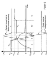
- FIG. 2 shows a typical example of the current commutation process between an IGBT in position S 2 1 and its corresponding freewheel diode FWD 1 2 during a hard switching.
- IGBTs the following description is primarily with respect to IGBTs, it is noteworthy that the circuit also suits other MOS-gated devices such as power MOSFETs.
- the voltage and current waveforms associated with the IGBT 1 and the freewheel diode 2 are usually depicted in five phases.
- the IGBT gate-emitter voltage V GE rises towards the gate threshold voltage V TH , whilst the IGBT 1 is still off.
- the IGBT collector-emitter voltage V CE starts to fall at the same time, because the rate of current change dI C / dt induces a voltage across the inductance L S . Since the load current I L is practically constant, when I C rises rapidly from zero to the level I L , the diode current I A decreases from its forward current, equal to I L , at an identical rate to zero. The excess carrier stored in the diode drift region is removed before the junction can become reverse biased.
- V CE completes its drop to the on-state voltage level in phase IV and phase V follows with the growth of V GE to V GG (on).
- a circuit diagram shows an embodiment of the present invention applied on an IGBT 1 and a freewheel diode 2. It comprises a gate drive circuit 3 and a control signal generating circuit 4.
- the gate drive circuit 3 comprising a high gain current buffer stage 31, a MOSFET drive stage 32 and a gate resistance R G 33, links the control signal generating circuit 4 and the IGBT gate terminal G.
- the control signal generating circuit 4 employs two feedback loops from the device power side: the V CE voltage feedback loop 41 and the di / dt feedback and conditioning loop 42.
- the voltage feedback loop 41 which may be composed of an array of resistors and capacitors, is attached to the collector terminal C of the IGBT 1 and the noninverting input of a very fast high-bandwidth operational amplifier 43.
- This operational amplifier 43 compares a scaled V CE with a reference function V REF 5 connected to its inverting input.
- the reference function 5 is generated by a high-speed FPGA (field programmable gate array) digital controller 44 and a DAC (digital to analogue converter) 45 in a specific manner described below, although alternative circuitry or microprocessor to perform the same function is possible.
- a self-timing method is proposed and realised via the di / dt feedback and conditioning circuit 42, which comprises a measuring means to detect said instant that is used to produce two distinctive stages according to the method and the circuit.
- the emitter Kelvin inductance L E 6 between the IGBT Kelvin terminal K and the emitter terminal E, may be used to fulfil this purpose.
- a timing control signal 46 is generated in the di / dt feedback and conditioning circuit 42 and fed back to the FPGA 44, which accordingly produces changes on the reference profile V REF 5.
- the FPGA 44 is connected through optical links or alternative means to other controllers (not shown) that can provide general on/off command signals.
- the two-stage voltage function is provided by the control signal generating circuit 4 to the IGBT gate terminal via the gate drive circuit 3.
- the reference function V REF 5 is characterised by an initial slowly-decreasing ramp 51 followed by a steeper ramp 52 and is in essence the two-stage voltage function used according to the method.
- the turning point 53 needs to coincide with said instant when the diode voltage starts to change from the on-state towards the off-state level.
- the IGBT current reaches its peak, the diode voltage has just begun to go negative.
- the self-timing method is proposed in this embodiment to detect the current rate change instead of diode voltage change.
- the timing requirement is fulfilled by the di / dt feedback and conditioning circuit 42, wherein a fast comparator may be used to monitor dI / dt and detect the instant when the voltage across the Kelvin inductance 6 changes the polarity.
- the di / dt feedback and conditioning circuit 42 generates a timing control signal 46 to instruct the FPGA 44 to terminate the first slow ramp 51 and to switch the reference function 5 to the second steeper ramp 52.
- This process features a self-timing control and therefore is the so-called self-timing method.
- alternative methods or ways may be employed to perform embodiments of a method according to the invention.
- the switching waveforms are optimised as shown in Figure 4 .
- the IGBT 1 is off and blocks a voltage equal to V DC , whilst the diode 2 is on with full current flow and a very low on-state voltage across it.
- the reference function 5 starts from a certain positive level V OFF 50 to a relatively slow ramp 51.
- the IGBT current I C rises from zero and the collector-emitter voltage V CE falls to track the reference ramp 51 according to a certain feedback ratio.
- V AK starts to change towards the off-state level
- the second steeper ramp 52 is initiated and V CE is directed to follow the diode voltage fall and to rapidly complete switch-on operation.
- V AK reaches V DC at time T 4
- the ramp 52 is terminated and the reference 5 is maintained at a negative voltage level V ON 54 until a switch-off command is given.
- an initial relatively slow ramp 51 circumscribes the decreasing rate of V CE and slows down the current rise of the IGBT 1, which results in lower current overshoots of both the IGBT 1 and the diode 2.
- the main fall of the IGBT voltage V CE is delayed until the diode 2 recovers and its voltage is ready to fall.
- controlled switching of both the IGBT 1 and the freewheel diode 2 substantially removes commonly seen diode reverse voltage overshoot and effectively reduces the current overshoots of both devices.
- the power dissipation during the switching process is optimised.
- This control process is a real-time self-optimisation independent of the operating conditions.
- the reference function 5 changes according to the real working conditions.
- both dV CE / dt and dI C / dt of the IGBT can be regulated through changing the ramp rate of the reference function 5. Close tracking between the IGBT voltage and the reference function 5 also allows devices in a series string to commence switch-on simultaneously when connected in series.
- the real-time optimisation concept and the circuit configuration also hold for the switch-off operation of a power semiconductor switching device.
- a well-controlled switch-off operation can also be realised.
- the power semiconductor switching device may be an IGBT, MOSFET, or a combination of such devices.
- the diode may be a standard recovery diode, a fast recovery diode, and a wide range of other types can also be used as freewheel diodes.
Landscapes
- Power Conversion In General (AREA)
- Electronic Switches (AREA)
- Networks Using Active Elements (AREA)
- Stabilization Of Oscillater, Synchronisation, Frequency Synthesizers (AREA)
- Amplifiers (AREA)
- Control Of Motors That Do Not Use Commutators (AREA)
Abstract
Description
- This invention generally relates to the control of power semiconductor devices, and in embodiments particularly relates to the concurrent control of power semiconductor switching devices and freewheel diodes.
- Power semiconductor devices are widely in use for a large range of power applications, from low voltage chips, computers, locomotives, to high voltage transmission lines. In most circuits, freewheel diodes need to be used in relation with the power semiconductor switching devices such as IGBTs (insulated gate bipolar transistors) or MOSFETs (metal oxide semiconductor field effect transistors) for a continuous load current conduction to avoid large voltage damaging the semiconductor devices and the circuit. High power IGBTs are often supplied as a module with diodes that act as freewheel diodes within the module. IGBTs are typically found in parallel with the diodes. Reliable switching operation of both a power semiconductor switching device and a freewheel diodes is of primary importance. Optimisation of the operation is also necessary to obtain high efficiency and low power dissipation of the whole circuit. In order to achieve these aims, one main concern is the current commutation from a freewheel diode to a power semiconductor switching device during the switch-on operation of the main switching device. Excessive diode voltage overshoot and power dissipation associated with the diode reverse recovery resulting from a poor commutation will impose high stresses on both the devices, limiting their application range. In particular, when there is a lack of good control, high power diodes may suffer from punch-through and a resulting snappy recovery with a sudden and large reverse voltage increase accompanied by high-frequency oscillation.
- Attempts have been made to control IGBTs and other power semiconductor switching devices by use of feedback control techniques including voltage, dv/dt, current and di/dt feedback control. Open loop networks are also widely employed. However, the freewheel diode cannot be directly controlled. Some lower power circuits even dispense with the diodes and use controlled switching devices in place of them. As a result, while those methods or gate drives embody some of the techniques described above, they fail to properly address the concurrent control of both the power semiconductor switching device and the conventional freewheel diode. They are frequently tailor-made to the application, where the user has to ensure that the commutation results in transient voltages and currents within bounds. Good control is difficult to achieve in many applications as the conditions such as load currents and temperatures are continuously changing. Even using feedback control, the result is highly empirical, and the need to adjust the gate drive for different operating conditions can make conventional methods very undesirable and inefficient.
- Background prior art can be found in
WO 9743832 US 2005253165 . - Granted European patent application
EP0508171 B1 (Siemens Aktiengesellschaft, Niedermeier Ernst, published 14.10.1992) relates to a switched-mode power output stage for inductive loads with a freewheeling circuit, in which both the rate of voltage change at the junction between load and switching device and the rate of change of the load current flowing through the switching device are attempted to be adjusted, the latter independently of the rate of voltage change. In this arrangement, a voltage proportional to the load current and a voltage proportional to the drain voltage are in each case differentiated and the signals thus obtained are superimposed on the control clock signal for the switching device. - Numerical Optimization of an Active Voltage Controller for Series IGBTs", Bryant et al, 2005 IEEE 36th Electronic Specialists Conference, pp. 2060-2065 describes simulations of IGBT control.
-
DE 102 11 077 A1 , Bakran et al, concerns a live method for mos - gate controlled power semiconductor devices. - According to a first aspect of the invention there is provided a method of controlling the commutation of a power semiconductor switching device and freewheel diode pair as defined in appended
independent claim 1. - According to a second aspect of the present invention, there is provided a circuit for implementing a method according to any one of appended
claims 1 to 5, the circuit for commutation of a power semiconductor switching device and freewheel diode pair as defined in appendedindependent claim 6. - Preferred embodiments are defined in the appended dependent claims.
- Preferred embodiments of the invention will now be described with reference to the accompanying drawings in which:
-
Figure 1 is a diagram showing an embodiment of a circuit according to the present invention employed in a half-bridge arm of an inverter. -
Figure 2 shows typical switching waveforms during a hard switch-on operation of an IGBT. -
Figure 3 is a diagram showing one specific circuit example of the present invention and of the circuitry inFigure 1 applied on an IGBT and freewheel diode pair. -
Figure 4 shows the voltage function generated by the circuitry ofFigure 1 or3 along with resulting switching waveforms when the method according to an embodiment of the present invention is employed. -
Figure 5 and6 show the switching waveforms without the good timing control which can be provided by embodiments of the present invention. - A first method is of controlling the commutation of a power semiconductor switching device and freewheel diode pair, the method comprising the stages of: applying, upon receipt of a switch-on command signal, a voltage function to a control terminal or the gate of the power semiconductor switching device, said voltage function allowing regulation of a current rise in the device whilst changing the voltage across the device; and substantially at the instant when the voltage across the diode (VAK) begins to change from an on-state towards an off-state voltage, applying a voltage function to the control terminal or the gate of the power semiconductor switching device to enable the voltage change across the power semiconductor switching device to substantially track the voltage change across the diode.
- The voltage function, that is the voltage shape or waveform, is in embodiments chosen to control the rate of change of the current and may comprise, a (slow) ramp or a (small) step, for example of around 10 per cent of the total change. By changing the switching device voltage in this way the current through the diode changes gradually (by contrast with a large step change in control voltage). In embodiments parasitic or other inductance in the circuit, more particularly in the series connected switching device and diode, results in a gradual change of current. In embodiments where voltage feedback is employed to control the switching an approximately linear ramp of current may be achieved.
- Broadly speaking in embodiments the concept is to change the voltage on the control terminal or gate of the active switching device using an initial ramp or step to determine when the passive switching device (diode) begins to switch. At this point the switching of the diode can be controlled by the active switch, thus enabling the switching of the active (IGBT) and passive (diode) switches to be synchronised. Thus embodiments of the method involve watching the diode to determine when it begins to switch; this point can be identified by identifying when the voltage across the diode begins to fall towards or through zero. One can define a sign convention such that when the diode is on the diode voltage is called positive and when the voltage begins to fall below zero and becomes negative the diode turns off- that is when the voltage across the diode reverses. The skilled person will appreciate, however, that the voltages across the active and passive switching devices operate as a see-saw, so that as one rises the other falls, and vice versa.
- In embodiments changing the voltage across the power semiconductor switching device comprises maintaining a falling voltage, at a pre-determined rate, across the device. However alternatively changing the voltage across this device may comprise maintaining the voltage to follow a predetermined waveform which may be stepped or linear (or piecewise linear) or both.
- In embodiments the method comprises synchronising the start of a voltage appearing across the freewheel diode (when the voltage across the diode begins to fall towards or through zero) with the main voltage fall of the power semiconductor switching device (that is when the diode begins switching) and a current peak in the power semiconductor switching device. In this way a safe and efficient current commutation substantially without diode reverse overshoot may be achieved. We illustrate later in reference to
figure 4 when the diode voltage (VAK) begins to switch (point T3 and dashed line to corner 53) but it can be seen in this figure that this point is not precisely coincident with the peak in diode current IC. The peak in IC is where the rate of change of current changes from positive to negative and thus is a conveniently identifiable feature on the diode current waveform. However it can be seen that this is not precisely coincident with the switching point of the diode although it is substantially at this instant (in embodiments we are slightly late). - In embodiments of the method the voltage function used to control the rate of voltage decrease across the power semiconductor switching device is determined by closed loop feedback monitoring. In embodiments the voltage function for controlling the power semiconductor switching device to track the diode voltage falling can be altered to ensure an optimum commutation process. That is in embodiments the voltage function (waveform) may be controlled to control the commutation process.
- A circuit for implementing a method as described above comprises: a gate drive circuit for providing a gate drive voltage for the power semiconductor switching device, and a control signal generating circuit, connected to the gate drive circuit, wherein upon receipt of a switch-on signal a first stage control signal is produced to control the gate drive circuit to drive the power semiconductor switching device to change said voltage across said device and a second stage control signal is generated, synchronised with the start of said voltage across said diode falling, to control the gate drive circuit to drive the voltage across the power semiconductor switching device to change substantially in synchronism with the diode voltage.
- As described above, in embodiments the voltages across the diode and across the power semiconductor switching device operate as a see-saw, that is the changes in voltage across these device substantially track one another. (If absolute voltage polarities are employed this may be expressed as both voltages falling at substantially the same rate).
- In embodiments the control signal generating circuit comprises a closed loop voltage feedback circuit to feedback a sensed voltage from the power semiconductor switching device and freewheel diode pair to the control signal generating circuit, and a current monitoring circuit to feedback a current sense signal from the device and diode pair to the control signal generating circuit. In embodiments both the first and second stage control signals are responsive to the sensed voltage and sensed current signal. In embodiments the sensed current signal senses a rate of change of the current through the device and diode pair.
- A further related arrangement is a circuit for controlling the commutation of a power semiconductor switching device and freewheel diode pair comprises: means for applying, upon receipt of a switch-on command signal a voltage function to a control terminal or the gate of the power semiconductor switching device, a current rise in the device whilst changing the voltage across the diode; and means for, substantially at the instant when the voltage across the diode begins to change from an on-state towards an off-state voltage, applying a voltage function to the control terminal or the gate of the power semiconductor switching device to enable the voltage change across the power semiconductor switching device to substantially track the voltage change across the diode.
- A still further related arrangement is a commutation control circuit for a chopper, said chopper comprising an active switching device and a passive switching device coupled in series, said commutation control circuit being configured to control commutation of said switching devices such that said switching devices switch substantially in synchronism, said control circuit comprising; a first sense input to receive a first sense signal from said chopper circuit; a second sense input to receive a second sense signal from said chopper circuit; and a control signal generating circuit coupled to said first and second sense inputs and having an output to control switching of said active switching device; and wherein said control signal generating circuit is configured to use said first and second sense signals to determine when said passive switch begins to switch and to control said active switching device such that said active and passive switching devices switch substantially in synchronism.
- In some preferred embodiments the commutation control circuit identifies a feature in a current sense signal sensing a current through the passive switching device, for example the polarity change of the rate change of diode current (or, in more accurately synchronised embodiments, the zero crossing of the diode voltage), to determine when the passive switch begins to switch. In embodiments the other sense signal comprises a voltage sense signal. In principle two voltage sense signals could be employed but this is less preferable because it is likely that for many applications one of the sensed voltages would be a relatively high voltage.
- In embodiments the control signal generating circuit comprises at least one digital control loop. For example a rate of change of current may be sensed and used to generate a (1 bit) timing control signal when the di/dt changes from positive to negative (or vice versa). This may be used to identify, approximately, a corner in the diode voltage, identifying a point at which the diode commences to switch. The control signal generating circuit may then generate a control signal to change the voltage on the active switch, for example the collector or emitter voltage of an IGBT, to bring this voltage down rapidly. In embodiments this may be performed by using digital circuitry to control a digital-to-analogue converter in response to the timing control signal. This function may be performed, for example, by high speed digital circuitry and implemented in an FPGA (field programmable gate array). Often switching times are of order nanoseconds and such an arrangement facilitates control on this timescale. Such arrangements facilitate control of the switching active and passive devices in synchronism.
- We will therefore describe a control method and a circuit for dynamically regulating switching operation of power semiconductor switching devices such as IGBTs or power MOSFETs, which addresses the aforementioned problems and allows control and optimisation of the commutation of a power semiconductor switching device and freewheel diode pair for a wide range of possible operating conditions.
- In embodiments the method comprises the stages of: applying, upon receipt of a switch-on command signal, a voltage function to the control terminal or the gate of the power semiconductor switching device that allows a regulated current rise in the device whilst maintaining the voltage across the device falling at a predetermined rate; and at substantially the instant when the voltage across the diode begins to change from the on-state towards the off-state level, applying a voltage function to the control terminal or the gate of the power semiconductor switching device to enable the voltage falling across the power semiconductor switching device to track the voltage falling across the diode in order to ensure a fast and controlled completion of the switching operation without diode reverse voltage overshoot.
- Said instant is determined by specific real-time device conditions instead of being preset. The gate drive automatically modifies the voltage function according to the working condition thereby accounting for the actual operating conditions. The particular relationship between the power switching device voltage and the diode voltage makes the method feature a so-called tracking control.
- By means of synchronising the start of the voltage appearing across the freewheel diode with the main voltage fall of the power semiconductor switching device during the switch-on process, the method is able to avoid the reverse recovery voltage overshoot of the freewheel diode and the high current spike of the power semiconductor switching device. It can therefore achieve a safe and efficient current and voltage commutation between the power semiconductor switching device and the freewheel diode with optimised switching losses and switching stresses below desired limits.
- Said two-stage voltage function applied to the gate of the power semiconductor switching device can be altered to ensure that the optimum switch-on characteristics are achieved for the particular switching device and diode being used and the conditions. Multiple loop feedback and monitoring of several variables such as current and voltage may be incorporated to produce said two-stage voltage function. The various techniques found in control theory may also be applied here with cascade control of the gate voltage as well as the power semiconductor switching device voltage, adaptive control of the features of said two-stage voltage function and so forth.
- In addition, the method is able to permit the regulation of the current rise rate of the power semiconductor switching device during its switch-on operation by circumscribing the voltage fall across the switching device in most conventional circuits which include stray inductance.
- Consequently, the method achieves a reliable control of the inherently non-linear transient behaviours of a power semiconductor switching devices and a freewheel diode, and optimises the performance of both devices in their SOAs (safe operating areas).
- Because of the controlled switching of both the power semiconductor switching device and the freewheel diode, embodiments of the present invention are also a good solution to serial device operation for high power applications, wherein series connection of power semiconductor switching devices such as IGBTs offers an alternative to high voltage thyristors. While IGBTs connected in series are each controlled in accordance with the present method, the switch-on behaviour of individual switch device can be synchronised and the interaction with diodes can be under control. Hence, traditional bulky and expensive switch-on snubber circuit for series connection can be avoided. We also describe a circuit for implementing a method as described above. In embodiments the circuit comprises: a gate drive circuit for providing the gate drive voltage to the control terminal or the gate of the power semiconductor switching device; and a control signal generating circuit, connected to the gate drive circuit, wherein, upon receipt of a switch-on signal, a first stage of control signal is produced to control the gate drive circuit to drive the power semiconductor switching device voltage to fall at a predetermined rate, and at substantially the instant when the diode voltage starts to change from the on-state towards the off-state level a second stage of control signal is generated to control the gate drive circuit to drive the power semiconductor switching device voltage to fall at the same or other rate to the diode voltage falling and to rapidly switch on the power semiconductor switching device.
- The control signal generating circuit may incorporate closed-loop circuits and voltage or current monitoring circuits.
- Preferably said instant for the circuit is determined by the change of the diode voltage, but it may instead be generated according to other variables. A simple self-timing method to create the two distinctive stages in said control signal is proposed in the following embodiment. In this the switching device current is monitored and the second stage of the switch-on is delayed until the current in the switching device changes the polarity of its rise rate. In embodiments this approach has the advantage of using feedback loops, making control circuit self-contained and compact.
- The skilled person will appreciate that various circuit approaches may be used for implementing the present method.
- Practical details will now be described with reference to the accompanying drawings.
-
Figure 1 shows the circuitry of an embodiment of the present invention applied in a half-bridge circuit, wherein two pairs of power semiconductor switching devices (S1, S2) and freewheel diodes (FWD1, FWD2) are connected as shown in the figure. The half-bridge configuration is the basic topology upon which most inverters are based. As shown inFigure 1 , a freewheel diode is placed in anti-parallel with each power semiconductor switching device. This arrangement normally constitutes a power module. When the upper switching device S1 is on, the lower device S2 is off, and vice-versa. The diodes FWD1 and FWD2 are to provide a path for the inductive load current IL. The current interaction betweenS 2 1 andFWD 1 2 is also shown. When the load current IL is flowing in the direction as specified inFigure 1 , the current is commutated fromFWD 1 2 toS 2 1 during a switch-on operation ofS 2 1. Agate drive circuit 3, connected to the gate terminal G2 for controllingS 2 1, is effectively a buffer circuit for a controlsignal generating circuit 4. The DC loop stray inductance LS , shown inFigure 1 , will also influence the switching, as a current change in LS will induce a voltage across it. -
Figure 2 shows a typical example of the current commutation process between an IGBT inposition S 2 1 and its correspondingfreewheel diode FWD 1 2 during a hard switching. Although the following description is primarily with respect to IGBTs, it is noteworthy that the circuit also suits other MOS-gated devices such as power MOSFETs. As shown inFigure 2 , the voltage and current waveforms associated with theIGBT 1 and thefreewheel diode 2 are usually depicted in five phases. During phase I, the IGBT gate-emitter voltage VGE rises towards the gate threshold voltage VTH, whilst theIGBT 1 is still off. As the IGBT collector current IC begins to rise at the start of phase II, the IGBT collector-emitter voltage VCE starts to fall at the same time, because the rate of current change dI C/ dt induces a voltage across the inductance LS . Since the load current IL is practically constant, when IC rises rapidly from zero to the level IL , the diode current IA decreases from its forward current, equal to IL, at an identical rate to zero. The excess carrier stored in the diode drift region is removed before the junction can become reverse biased. Thus IA falls below zero to draw reverse recovery current and IC increases above the level IL , reaching the peak IL+IRR at the end of phase II, by which point thediode 2 has begun to regain reverse blocking capability. During phase III, the growing reverse voltage across thediode 2 causes VCE to decrease rapidly. With VCE approaching zero and IC reducing, an overshoot VRR usually appears in VAK. The relationship between VAK, VCE and IC is revealed in the following equation:
- The dIC /dt occurring during the reduction in IC to the load current level IL in the absence of concurrent control over VCE and VAK makes the diode voltage reverse overshoot VRR very likely. VCE completes its drop to the on-state voltage level in phase IV and phase V follows with the growth of VGE to VGG(on).
- Referring to
Figure 3 , a circuit diagram shows an embodiment of the present invention applied on anIGBT 1 and afreewheel diode 2. It comprises agate drive circuit 3 and a controlsignal generating circuit 4. - The
gate drive circuit 3, comprising a high gaincurrent buffer stage 31, aMOSFET drive stage 32 and agate resistance R G 33, links the controlsignal generating circuit 4 and the IGBT gate terminal G. - The control
signal generating circuit 4 employs two feedback loops from the device power side: the VCEvoltage feedback loop 41 and the di/dt feedback andconditioning loop 42. Thevoltage feedback loop 41, which may be composed of an array of resistors and capacitors, is attached to the collector terminal C of theIGBT 1 and the noninverting input of a very fast high-bandwidthoperational amplifier 43. Thisoperational amplifier 43 compares a scaled VCE with areference function V REF 5 connected to its inverting input. Thereference function 5 is generated by a high-speed FPGA (field programmable gate array)digital controller 44 and a DAC (digital to analogue converter) 45 in a specific manner described below, although alternative circuitry or microprocessor to perform the same function is possible. In this embodiment a self-timing method is proposed and realised via the di/dt feedback andconditioning circuit 42, which comprises a measuring means to detect said instant that is used to produce two distinctive stages according to the method and the circuit. The emitterKelvin inductance L E 6, between the IGBT Kelvin terminal K and the emitter terminal E, may be used to fulfil this purpose. Atiming control signal 46 is generated in the di/dt feedback andconditioning circuit 42 and fed back to theFPGA 44, which accordingly produces changes on thereference profile V REF 5. TheFPGA 44 is connected through optical links or alternative means to other controllers (not shown) that can provide general on/off command signals. - According to an embodiment of the present invention, the two-stage voltage function is provided by the control
signal generating circuit 4 to the IGBT gate terminal via thegate drive circuit 3. Referring toFigure 4 , in this particular embodiment thereference function V REF 5 is characterised by an initial slowly-decreasingramp 51 followed by asteeper ramp 52 and is in essence the two-stage voltage function used according to the method. Theturning point 53 needs to coincide with said instant when the diode voltage starts to change from the on-state towards the off-state level. As observed inFigure 2 , when the IGBT current reaches its peak, the diode voltage has just begun to go negative. Furthermore, the current peak point actually happens when dICldt changes from positive to negative, inducing a voltage polarity change across theemitter Kelvin inductance 6. Consequently, the self-timing method is proposed in this embodiment to detect the current rate change instead of diode voltage change. The timing requirement is fulfilled by the di/dt feedback andconditioning circuit 42, wherein a fast comparator may be used to monitor dI/dt and detect the instant when the voltage across theKelvin inductance 6 changes the polarity. At this instant, the di/dt feedback andconditioning circuit 42 generates atiming control signal 46 to instruct theFPGA 44 to terminate the firstslow ramp 51 and to switch thereference function 5 to the secondsteeper ramp 52. This process features a self-timing control and therefore is the so-called self-timing method. Again alternative methods or ways may be employed to perform embodiments of a method according to the invention. - Under the regulation of the two-stage
voltage function V REF 5 according to an embodiment of the present invention, the switching waveforms are optimised as shown inFigure 4 . At a time zero, theIGBT 1 is off and blocks a voltage equal to VDC, whilst thediode 2 is on with full current flow and a very low on-state voltage across it. At time T1, thereference function 5 starts from a certainpositive level V OFF 50 to a relativelyslow ramp 51. From time T2, the IGBT current IC rises from zero and the collector-emitter voltage VCE falls to track thereference ramp 51 according to a certain feedback ratio. At time T3, when VAK starts to change towards the off-state level, the secondsteeper ramp 52 is initiated and VCE is directed to follow the diode voltage fall and to rapidly complete switch-on operation. After VAK reaches VDC at time T4, theramp 52 is terminated and thereference 5 is maintained at a negativevoltage level V ON 54 until a switch-off command is given. From time T1 to T3, an initial relativelyslow ramp 51 circumscribes the decreasing rate of VCE and slows down the current rise of theIGBT 1, which results in lower current overshoots of both theIGBT 1 and thediode 2. The main fall of the IGBT voltage VCE is delayed until thediode 2 recovers and its voltage is ready to fall. Such tracking reduces the voltage seen by the combination of the stray inductance LS and the diode junction capacitance. As a good synchronisation between thereference turning point 53 and the instant of the diode voltage fall is maintained by the tracking control, the decrease of VAK is a smooth reduction, which completely avoids diode reverse voltage overshoot. A slight inflexion in the middle of the diode voltage drop emerges, marking a change of the voltage decreasing rate. This can be explained according toEquation 1. While VCE, VAK and IC are falling, VAK decrease at a faster rate than VCE because of the changing voltage created across LS. When VCE has dropped to a low value, IC enters a smooth decay period. - Preferably (but not essentially) good timing between the instant when the diode voltage begins to change towards the off-state level and the reference
function turning point 53 is used in the method to obtain an optimal performance. By comparison, two scenarios without good timing control in this embodiment are shown inFigure 5 andFigure 6 . When the synchronisation between thereference turning point 53 and the desired instant cannot be realised, the optimal switching performance, as shown inFigure 4 , will be lost. InFigure 5 , when the VREF turning point 53 is lagging behind the start of the diode voltage change, there is a high current overshoot and the diode reverse voltage overshoot occurs too early, marking a kink in the middle of the diode voltage. Although the diode voltage does not overshoot beyond -VDC, both the current overshoot stress and switching power losses are increased. When theturning point 53 is leading the desired instant as shown inFigure 6 , the overshoot in the diode voltage VAK reappears accompanied by a very high IGBT current overshoot. The overall power losses may be slightly reduced compared to that under the good timing control; however, the rating margins in both current and voltage are largely reduced. - By use of embodiments of the present invention, controlled switching of both the
IGBT 1 and thefreewheel diode 2 substantially removes commonly seen diode reverse voltage overshoot and effectively reduces the current overshoots of both devices. The power dissipation during the switching process is optimised. This control process is a real-time self-optimisation independent of the operating conditions. As the self-timing control stands, thereference function 5 changes according to the real working conditions. Furthermore, both dVCE /dt and dIC /dt of the IGBT can be regulated through changing the ramp rate of thereference function 5. Close tracking between the IGBT voltage and thereference function 5 also allows devices in a series string to commence switch-on simultaneously when connected in series. - The real-time optimisation concept and the circuit configuration also hold for the switch-off operation of a power semiconductor switching device. By monitoring the power states and changing the reference function accordingly, a well-controlled switch-off operation can also be realised.
- The power semiconductor switching device may be an IGBT, MOSFET, or a combination of such devices. The diode may be a standard recovery diode, a fast recovery diode, and a wide range of other types can also be used as freewheel diodes.
- It will be understood that the invention is not limited to the described embodiments and modifications can be made within the scope of the claims appended hereto.
Claims (7)
- A method of controlling the commutation of a series-connected power semiconductor switching device (1) and freewheel diode (2) pair of a half-bridge arm of an inverter, the half-bridge arm comprising a load connection between said device and freewheel diode, the power semiconductor switching device in a lower voltage side of the load connection than the diode, the method comprising the stages of:applying, upon receipt of a switch-on command signal, a first waveform stage of a voltage function to a control terminal or the gate (G) of the power semiconductor switching device (1), said first waveform stage of said voltage function allowing regulation of a current rise in the device (1) whilst changing voltage across the device (1);detecting a feature in a current or voltage sense signal of said pair, said feature substantially at the instant when voltage (VAK) across the diode (2) begins to change from an on-state towards an off-state voltage during said applied first waveform stage of said voltage function;generating a reference function and producing a change in profile of said reference function responsive to said detection to thereby change said voltage function from said first waveform stage to a second waveform stage, wherein reference function has a first waveform portion comprising a first decreasing ramp and a second waveform portion comprising a steeper decreasing ramp and said change of said profile of said reference function is from said first ramp to said second ramp;applying substantially at said instant said second waveform stage of said voltage function to the control terminal or the gate (G) of the power semiconductor switching device (1) to enable the voltage change across the power semiconductor switching device (1) to substantially track the voltage change across the diode (2),controlling voltage change across the power semiconductor switching device (1) during applying said first and second waveform stages, on the basis of comparison of said reference function and a scaled voltage of said semiconductor switching device (1),wherein said power semiconductor switching device (1) is an Insulated Gate Bipolar Transistor, said feature is a peak current of said Insulated Gate Bipolar Transistor, and said detecting said feature comprises using a comparator to detect an instant when a voltage across an inductance between a Kelvin terminal of said Insulated Gate Bipolar Transistor (1) and an emitter terminal of said Insulated Gate Bipolar Transistor (1) changes polarity.
- A method as claimed in claim 1 wherein said changing of said voltage across said device (1) comprises maintaining said voltage falling (51) according to a predetermined rate.
- A method according to claim 1 or 2, further comprising synchronising a start of a reverse voltage appearing across the freewheel diode (2) with the start of the voltage fall of the power semiconductor switching device (1) when said diode (2) begins switching and a current peak in the power semiconductor switching device (1), such that current commutation substantially without diode-reverse overshoot is achieved.
- A method according to claim 1, 2, or 3 wherein said voltage function is determined by the use of closed-loop feedback monitoring.
- A method according to any one of claims 1 to 4 further comprising altering said voltage function to alter said commutation process.
- A circuit for commutation of a series-connected power semiconductor switching device (1) and freewheel diode (2) pair of a half-bridge arm of an inverter, the half-bridge arm comprising a load connection between said device and freewheel diode, the power semiconductor switching device in a lower voltage side of the load connection than the diode, the circuit comprising:a gate drive circuit (3) for providing a gate drive voltage for the power semiconductor switching device (1); anda control signal generating circuit (4), connected to the gate drive circuit (3), wherein said control signal generating circuit (4) is configured to:produce, upon receipt of a switch-on signal, a first stage of a control signal to control the gate drive circuit (3) to drive the power semiconductor switching device (1) to change voltage across said device (1);detect a feature in a current or voltage sense signal of said pair, said feature substantially at an instant when voltage (VAK) across the diode (2) begins to change from an on-state towards an off-state voltage during said produced first stage of said control signal; andgenerate a reference function and produce a change in profile of said reference function responsive to said detection to thereby change said control signal from said first stage to a second stage, said second stage of said control signal synchronised with the start of said voltage (VAK) across said diode (2) falling, to control the gate drive circuit (3) to drive the voltage across the power semiconductor switching device (1) to change substantially in synchronism with the diode voltage, wherein said reference function comprises a first decreasing ramp followed by a steeper decreasing ramp and said change in profile is from said first ramp to said second ramp;
wherein the circuit for commutation of a power semiconductor switching device and freewheel pair comprises:a feedback loop arranged to control voltage change across the power semiconductor switching device (1) during said first and second stages of said control signal dependent on comparison of said reference function and a scaled voltage of said semiconductor switching device (1), whereinsaid power semiconductor switching device (1) is an Insulated Gate Bipolar Transistor and said feature is a peak current of said Insulated Gate Bipolar Transistor, andthe circuit for commutation of a power semiconductor switching device and freewheel pair comprises a comparator and an inductance between a Kelvin terminal of said Insulated Gate Bipolar Transistor (1) and an emitter terminal of said Insulated Gate Bipolar Transistor (1), and wherein the control signal generating circuit is configured to use said comparator to detect an instant when a voltage across said inductance changes polarity to thereby perform said detecting said feature. - A circuit according to claim 6, wherein said control signal generating circuit (4) comprises a closed-loop voltage feedback circuit to feedback a sensed voltage from said power semiconductor switching device (1) and freewheel diode (2) pair to said control signal generating circuit (4), and a current monitoring circuit to feedback a current sense signal from said power semiconductor switching device (1) and freewheel diode (2) pair to said control signal generating circuit (4), and wherein said first and second stages of said control signal are responsive to said sensed voltage and said current sense signal.
Applications Claiming Priority (2)
| Application Number | Priority Date | Filing Date | Title |
|---|---|---|---|
| GBGB0617990.7A GB0617990D0 (en) | 2006-09-13 | 2006-09-13 | Control of power semiconductor devices |
| PCT/GB2007/050531 WO2008032113A1 (en) | 2006-09-13 | 2007-09-10 | Control method and circuit for power semiconductor devices |
Publications (3)
| Publication Number | Publication Date |
|---|---|
| EP2089968A1 EP2089968A1 (en) | 2009-08-19 |
| EP2089968B1 EP2089968B1 (en) | 2011-02-16 |
| EP2089968B2 true EP2089968B2 (en) | 2014-03-12 |
Family
ID=37232833
Family Applications (1)
| Application Number | Title | Priority Date | Filing Date |
|---|---|---|---|
| EP07804437.7A Not-in-force EP2089968B2 (en) | 2006-09-13 | 2007-09-10 | Control method and circuit for power semiconductor devices |
Country Status (8)
| Country | Link |
|---|---|
| US (1) | US8004317B2 (en) |
| EP (1) | EP2089968B2 (en) |
| JP (1) | JP5122571B2 (en) |
| CN (1) | CN101617471B (en) |
| AT (1) | ATE498945T1 (en) |
| DE (1) | DE602007012576D1 (en) |
| GB (1) | GB0617990D0 (en) |
| WO (1) | WO2008032113A1 (en) |
Families Citing this family (59)
| Publication number | Priority date | Publication date | Assignee | Title |
|---|---|---|---|---|
| US7928774B2 (en) * | 2008-09-29 | 2011-04-19 | Infineon Technologies Ag | Adaptive drive signal adjustment for bridge EMI control |
| US8985850B1 (en) * | 2009-10-30 | 2015-03-24 | Cypress Semiconductor Corporation | Adaptive gate driver strength control |
| JP5895170B2 (en) * | 2010-02-23 | 2016-03-30 | パナソニックIpマネジメント株式会社 | 2-wire AC switch |
| DE102010015399B3 (en) * | 2010-02-25 | 2011-02-17 | Siemens Aktiengesellschaft | Driver output stage for a power IGBT |
| JP5460519B2 (en) | 2010-08-09 | 2014-04-02 | 本田技研工業株式会社 | Semiconductor device driving apparatus and method |
| US8749278B2 (en) * | 2010-08-09 | 2014-06-10 | Honda Motor Co., Ltd. | Semiconductor device driving unit and method |
| GB2488778B (en) | 2011-03-07 | 2013-03-20 | Amantys Ltd | Voltage balancing for power switching devices |
| CN108964442A (en) | 2011-05-05 | 2018-12-07 | 北极砂技术有限公司 | Device for power supply conversion |
| US10680515B2 (en) | 2011-05-05 | 2020-06-09 | Psemi Corporation | Power converters with modular stages |
| DE102011077387A1 (en) | 2011-06-10 | 2012-07-12 | Siemens Aktiengesellschaft | Circuit arrangement for switching current in dependence of predeterminable switching signal, has semiconductor circuit breaker for controlling current intensity and driver circuit for receiving switching signal |
| US8760215B2 (en) * | 2011-07-15 | 2014-06-24 | Delphi Technologies, Inc. | Threshold voltage based power transistor operation |
| DE102011079552B4 (en) | 2011-07-21 | 2014-05-08 | Siemens Aktiengesellschaft | Circuit for switching a current and method for operating a semiconductor power switch |
| DE102011079545A1 (en) | 2011-07-21 | 2013-01-24 | Siemens Aktiengesellschaft | Circuit arrangement with a semiconductor switch and an associated drive circuit |
| JP5932269B2 (en) * | 2011-09-08 | 2016-06-08 | 株式会社東芝 | Power semiconductor module and driving method of power semiconductor module |
| US8743553B2 (en) | 2011-10-18 | 2014-06-03 | Arctic Sand Technologies, Inc. | Power converters with integrated capacitors |
| WO2013075749A1 (en) * | 2011-11-24 | 2013-05-30 | Ebm-Papst Mulfingen Gmbh & Co. Kg | Electronic circuit and method for triggering a semiconductor switch |
| US8723491B2 (en) | 2011-12-19 | 2014-05-13 | Arctic Sand Technologies, Inc. | Control of power converters with capacitive energy transfer |
| CN103166435B (en) * | 2011-12-19 | 2014-12-03 | 中国电力科学研究院 | Voltage self-adaptive control method based on insulated gate bipolar translator (IGBT) series connection loss optimization |
| GB2497970A (en) * | 2011-12-23 | 2013-07-03 | Amantys Ltd | Power semiconductor switching device controller |
| EP2615737B1 (en) | 2012-01-13 | 2021-05-05 | ABB Schweiz AG | Active gate drive circuit |
| GB201206921D0 (en) * | 2012-04-20 | 2012-06-06 | Amantys Ltd | Communication protocol |
| US9048831B2 (en) * | 2012-07-13 | 2015-06-02 | General Electric Company | Systems and methods for regulating semiconductor devices |
| EP2768140A1 (en) | 2013-02-13 | 2014-08-20 | Alstom Technology Ltd | Method of switching a semiconductor device |
| US8619445B1 (en) | 2013-03-15 | 2013-12-31 | Arctic Sand Technologies, Inc. | Protection of switched capacitor power converter |
| US8724353B1 (en) | 2013-03-15 | 2014-05-13 | Arctic Sand Technologies, Inc. | Efficient gate drivers for switched capacitor converters |
| DK2942870T3 (en) | 2014-05-09 | 2018-10-22 | Abb Schweiz Ag | Device and method for a power semiconductor contact |
| KR102688244B1 (en) | 2015-03-13 | 2024-07-24 | 피세미 코포레이션 | DC-DC transformer with an inductor to facilitate charge transport between insulating capacitors |
| US9793890B2 (en) * | 2015-05-07 | 2017-10-17 | Infineon Technologies Austria Ag | System and method for a switch transistor driver |
| CN108028600B (en) | 2015-07-08 | 2022-03-08 | 派更半导体公司 | Switched Capacitor Power Converters |
| CN105048773A (en) * | 2015-07-23 | 2015-11-11 | 深圳开立生物医疗科技股份有限公司 | Output voltage control circuit |
| EP3174205A1 (en) * | 2015-11-27 | 2017-05-31 | ABB Technology Oy | Control circuit with feedback |
| CN107154791A (en) * | 2016-03-02 | 2017-09-12 | 国网辽宁省电力有限公司电力科学研究院 | The electric current rate of rise detection circuit and its detection method of high-power IGBT module |
| KR102449361B1 (en) * | 2016-04-08 | 2022-09-30 | 삼성전기주식회사 | linear current driver |
| CN105790743A (en) * | 2016-04-13 | 2016-07-20 | 中国人民解放军国防科学技术大学 | Active source voltage control large power IGBT method and system |
| DE102016111449A1 (en) * | 2016-06-22 | 2017-12-28 | Infineon Technologies Ag | Circuit and method for driving a power semiconductor device |
| EP3270513B1 (en) * | 2016-07-11 | 2019-07-03 | NXP USA, Inc. | Igbt gate current slope measure to estimate miller plateau |
| CN105932864B (en) * | 2016-07-18 | 2018-11-16 | 南京埃斯顿自动控制技术有限公司 | A kind of intelligentized IGBT constant current driving device |
| CN106357252A (en) * | 2016-09-05 | 2017-01-25 | 安徽中研电气有限责任公司 | Fully digitalized IGBT (insulated gate bipolar transistor) driving controller |
| GB201620104D0 (en) * | 2016-11-28 | 2017-01-11 | Powerventure Semiconductor Ltd | A system and method of driving a switch circuit |
| EP3641113B1 (en) * | 2017-05-16 | 2022-05-11 | Fuji Electric Co., Ltd. | Control device and semiconductor apparatus |
| CN107819461B (en) * | 2017-09-29 | 2021-02-12 | 杭州飞仕得科技有限公司 | Numerical control active IGBT drive circuit |
| US10461732B1 (en) * | 2018-06-18 | 2019-10-29 | Infineon Technologies Austria Ag | System and method of driving a power switch in combination with regulated DI/DT and/or DV/DT |
| CN108964643A (en) * | 2018-06-27 | 2018-12-07 | 深圳市汇北川电子技术有限公司 | A kind of drive control circuit and control method of the power device at current mirror end |
| CN109240408B (en) * | 2018-10-31 | 2020-09-25 | 西安理工大学 | SicMOSFET gate drive voltage control circuit and control method thereof |
| CN109412394A (en) * | 2018-11-01 | 2019-03-01 | 湖南大学 | Inhibit the open loop active voltage driving circuit and method of IGBT and MOSFET electromagnetic interference |
| CN111262567B (en) * | 2018-11-30 | 2023-06-23 | 株洲中车时代半导体有限公司 | An active gate drive control circuit and control method |
| US10720913B1 (en) * | 2019-05-28 | 2020-07-21 | Infineon Technologies Austria Ag | Integrated failsafe pulldown circuit for GaN switch |
| US10958268B1 (en) | 2019-09-04 | 2021-03-23 | Infineon Technologies Austria Ag | Transformer-based driver for power switches |
| EP3849083A1 (en) * | 2020-01-07 | 2021-07-14 | Hamilton Sundstrand Corporation | Gate driver |
| US10979032B1 (en) | 2020-01-08 | 2021-04-13 | Infineon Technologies Austria Ag | Time-programmable failsafe pulldown circuit for GaN switch |
| CN111208410B (en) * | 2020-01-13 | 2025-03-28 | 北京华峰测控技术股份有限公司 | A voltage and current source test circuit and test method |
| CN111313874A (en) * | 2020-03-18 | 2020-06-19 | 上海海事大学 | Current detection device for SiC MOSFET and short-circuit protection method |
| CN111294034B (en) * | 2020-03-23 | 2024-04-02 | 广东美的白色家电技术创新中心有限公司 | Gate drive circuit, power switch circuit and electrical equipment |
| CN112953481B (en) * | 2021-01-27 | 2022-09-27 | 复旦大学 | Drive module, switching circuit and electronic equipment of GaN transistor |
| WO2022254569A1 (en) * | 2021-06-01 | 2022-12-08 | 三菱電機株式会社 | Power semiconductor element drive adjustment circuit, power module, and power conversion device |
| US12176887B2 (en) | 2022-10-17 | 2024-12-24 | Infineon Technologies Austria Ag | Transformer-based drive for GaN devices |
| CN116106716A (en) * | 2023-02-28 | 2023-05-12 | 苏州鉴芯信息科技有限公司 | A device off-time detection system for power electronic bridge arm components |
| US12368383B2 (en) | 2023-03-13 | 2025-07-22 | Infineon Technologies Austria Ag | Isolated DC/DC converter and power electronics system |
| CN116317477B (en) * | 2023-03-20 | 2025-09-19 | 武汉大学 | Gate electrode staged driving circuit based on DAC digital signal feedback |
Citations (1)
| Publication number | Priority date | Publication date | Assignee | Title |
|---|---|---|---|---|
| DE10211077A1 (en) † | 2002-03-13 | 2003-09-04 | Siemens Ag | Drive method for MOS-gate controlled power semiconductor devices, by driving with gate current that limits rate of rise of collector current, and then increasing |
Family Cites Families (12)
| Publication number | Priority date | Publication date | Assignee | Title |
|---|---|---|---|---|
| US4661766A (en) * | 1985-12-23 | 1987-04-28 | Caterpillar Inc. | Dual current sensing driver circuit |
| DE3730503A1 (en) * | 1987-09-11 | 1989-03-30 | Walter Marks | DC control circuit |
| US5055721A (en) * | 1989-04-13 | 1991-10-08 | Mitsubishi Denki Kabushiki Kaisha | Drive circuit for igbt device |
| US4967309A (en) * | 1989-12-26 | 1990-10-30 | Caterpillar Inc. | Dual current sensing driver circuit |
| EP0508171B1 (en) * | 1991-04-11 | 1997-06-25 | Siemens Aktiengesellschaft | Switching mode power output stage for inductive loads |
| GB9610098D0 (en) | 1996-05-15 | 1996-07-17 | Palmer Patrick R | Insulated gate bipolar transistor control |
| US5912552A (en) * | 1997-02-12 | 1999-06-15 | Kabushiki Kaisha Toyoda Jidoshokki Seisakusho | DC to DC converter with high efficiency for light loads |
| CN1312973A (en) * | 1998-06-12 | 2001-09-12 | 南岛分立有限公司 | Gate drive for insulated gate power semiconductors |
| US6127815A (en) * | 1999-03-01 | 2000-10-03 | Linear Technology Corp. | Circuit and method for reducing quiescent current in a switching regulator |
| DE10231198A1 (en) * | 2002-07-10 | 2004-01-29 | eupec Europäische Gesellschaft für Leistungshalbleiter mbH | Method and circuit arrangement for limiting an overvoltage |
| DE102004013108B4 (en) * | 2004-03-17 | 2011-03-10 | Beckhoff Automation Gmbh | Method for operating a supply unit for a driver circuit and supply unit for a driver circuit |
| CN101088221B (en) | 2004-04-26 | 2011-08-10 | 勒图尔纽科技钻孔系统公司 | Self-adaption gate drive circuit and method for switching devices of inverter, and inverter |
-
2006
- 2006-09-13 GB GBGB0617990.7A patent/GB0617990D0/en not_active Ceased
-
2007
- 2007-09-10 EP EP07804437.7A patent/EP2089968B2/en not_active Not-in-force
- 2007-09-10 JP JP2009527901A patent/JP5122571B2/en not_active Expired - Fee Related
- 2007-09-10 CN CN200780042245.9A patent/CN101617471B/en not_active Expired - Fee Related
- 2007-09-10 DE DE602007012576T patent/DE602007012576D1/en active Active
- 2007-09-10 US US12/441,128 patent/US8004317B2/en not_active Expired - Fee Related
- 2007-09-10 WO PCT/GB2007/050531 patent/WO2008032113A1/en not_active Ceased
- 2007-09-10 AT AT07804437T patent/ATE498945T1/en not_active IP Right Cessation
Patent Citations (1)
| Publication number | Priority date | Publication date | Assignee | Title |
|---|---|---|---|---|
| DE10211077A1 (en) † | 2002-03-13 | 2003-09-04 | Siemens Ag | Drive method for MOS-gate controlled power semiconductor devices, by driving with gate current that limits rate of rise of collector current, and then increasing |
Non-Patent Citations (3)
| Title |
|---|
| A.T. BRYANT ET AL: "Numerical Optimization of an Active Voltage Controller for Series IGBTs", IEEE 36TH ELECTRONIC SPECIALISTS CONFERENCE (PESC), 2005 - 2005, pages 2060 - 2065, XP031000424 † |
| CHRISTIAN GERSTER, PATRICK HOFER: "Gate-controlled dv/dt- and di/dt-limitation in high power IGBT converters", EPE JOURNAL, vol. 5, no. 3/4, January 1996 (1996-01-01) - January 1996 (1996-01-01), pages 11 - 16, XP002344531 † |
| Y. WANG, A.T. BRYANT ET AL.: "An Analysis of High Power IGBT Switching under Cascade Active Voltage Control", IEEE IAS, 2005 - 2005, pages 806 - 812, XP010842474 † |
Also Published As
| Publication number | Publication date |
|---|---|
| WO2008032113A1 (en) | 2008-03-20 |
| EP2089968A1 (en) | 2009-08-19 |
| DE602007012576D1 (en) | 2011-03-31 |
| CN101617471A (en) | 2009-12-30 |
| EP2089968B1 (en) | 2011-02-16 |
| CN101617471B (en) | 2012-12-19 |
| JP2010528570A (en) | 2010-08-19 |
| JP5122571B2 (en) | 2013-01-16 |
| GB0617990D0 (en) | 2006-10-18 |
| US20100060326A1 (en) | 2010-03-11 |
| ATE498945T1 (en) | 2011-03-15 |
| US8004317B2 (en) | 2011-08-23 |
Similar Documents
| Publication | Publication Date | Title |
|---|---|---|
| EP2089968B1 (en) | Control method and circuit for power semiconductor devices | |
| Zhang et al. | Advanced active gate drive for switching performance improvement and overvoltage protection of high-power IGBTs | |
| US7710187B2 (en) | Gate drive circuit | |
| US8363440B2 (en) | Power conversion circuit having off-voltage control circuit | |
| EP4102720A1 (en) | Actively tracking switching speed control and regulating switching speed of a power transistor during turn-on | |
| KR102324451B1 (en) | Actively tracking switching speed control of a power transistor | |
| KR20120030411A (en) | Gate driver for enhancement-mode and depletion-mode wide bandgap semiconductor jefts | |
| CN106463948B (en) | MOSFET Driver with Pulse Timing Mode Fault Detection and Adaptive Safe Run Region Operation Mode | |
| CN109842279B (en) | A SiC MOSFET open-loop active drive circuit | |
| US11843368B2 (en) | Method for reducing oscillation during turn on of a power transistor by regulating the gate switching speed control of its complementary power transistor | |
| US11444613B1 (en) | Actively tracking switching speed control and regulating switching speed of a power transistor during turn-on | |
| Jones et al. | Active gate drive to increase the power capacity of hard-switched IGBTs | |
| CN112821730A (en) | Novel driving topology and driving method and crosstalk suppression method thereof | |
| Wang et al. | High-frequency three-level gate driver for GaN HEMT bridge crosstalk suppression | |
| Jones et al. | Investigation of IGBT switching energy loss and peak overvoltage using digital active gate drives | |
| CN216699815U (en) | Novel driving topology | |
| Handt et al. | Fully digitised, quasi-continuous working gate-drive unit for 1200V-IGBT | |
| US11664741B2 (en) | System and method for AC power control | |
| JPH07212207A (en) | Square wave constant current generation circuit | |
| Lopez et al. | Method for the analysis of power MOSFET losses in a synchronous buck converter | |
| JPH06105448A (en) | Switch device with protection function | |
| EP4734369A1 (en) | Current source gate driver | |
| US12620905B2 (en) | Methods and apparatus for controlling switching in power converters | |
| Wang et al. | A gate drive circuit of high power IGBTs for improved turn-on characteristics under hard switching conditions | |
| Wen et al. | A di/dt and dv/dt feedback-based digital gate driver for smart switching of IGBT modules |
Legal Events
| Date | Code | Title | Description |
|---|---|---|---|
| PUAI | Public reference made under article 153(3) epc to a published international application that has entered the european phase |
Free format text: ORIGINAL CODE: 0009012 |
|
| 17P | Request for examination filed |
Effective date: 20090408 |
|
| AK | Designated contracting states |
Kind code of ref document: A1 Designated state(s): AT BE BG CH CY CZ DE DK EE ES FI FR GB GR HU IE IS IT LI LT LU LV MC MT NL PL PT RO SE SI SK TR |
|
| 17Q | First examination report despatched |
Effective date: 20090814 |
|
| DAX | Request for extension of the european patent (deleted) | ||
| GRAP | Despatch of communication of intention to grant a patent |
Free format text: ORIGINAL CODE: EPIDOSNIGR1 |
|
| GRAS | Grant fee paid |
Free format text: ORIGINAL CODE: EPIDOSNIGR3 |
|
| GRAA | (expected) grant |
Free format text: ORIGINAL CODE: 0009210 |
|
| AK | Designated contracting states |
Kind code of ref document: B1 Designated state(s): AT BE BG CH CY CZ DE DK EE ES FI FR GB GR HU IE IS IT LI LT LU LV MC MT NL PL PT RO SE SI SK TR |
|
| REG | Reference to a national code |
Ref country code: GB Ref legal event code: FG4D |
|
| REG | Reference to a national code |
Ref country code: CH Ref legal event code: EP |
|
| REG | Reference to a national code |
Ref country code: IE Ref legal event code: FG4D |
|
| REF | Corresponds to: |
Ref document number: 602007012576 Country of ref document: DE Date of ref document: 20110331 Kind code of ref document: P |
|
| REG | Reference to a national code |
Ref country code: DE Ref legal event code: R096 Ref document number: 602007012576 Country of ref document: DE Effective date: 20110331 |
|
| REG | Reference to a national code |
Ref country code: NL Ref legal event code: VDEP Effective date: 20110216 |
|
| LTIE | Lt: invalidation of european patent or patent extension |
Effective date: 20110216 |
|
| PG25 | Lapsed in a contracting state [announced via postgrant information from national office to epo] |
Ref country code: ES Free format text: LAPSE BECAUSE OF FAILURE TO SUBMIT A TRANSLATION OF THE DESCRIPTION OR TO PAY THE FEE WITHIN THE PRESCRIBED TIME-LIMIT Effective date: 20110527 Ref country code: SE Free format text: LAPSE BECAUSE OF FAILURE TO SUBMIT A TRANSLATION OF THE DESCRIPTION OR TO PAY THE FEE WITHIN THE PRESCRIBED TIME-LIMIT Effective date: 20110216 Ref country code: LT Free format text: LAPSE BECAUSE OF FAILURE TO SUBMIT A TRANSLATION OF THE DESCRIPTION OR TO PAY THE FEE WITHIN THE PRESCRIBED TIME-LIMIT Effective date: 20110216 Ref country code: PT Free format text: LAPSE BECAUSE OF FAILURE TO SUBMIT A TRANSLATION OF THE DESCRIPTION OR TO PAY THE FEE WITHIN THE PRESCRIBED TIME-LIMIT Effective date: 20110616 Ref country code: GR Free format text: LAPSE BECAUSE OF FAILURE TO SUBMIT A TRANSLATION OF THE DESCRIPTION OR TO PAY THE FEE WITHIN THE PRESCRIBED TIME-LIMIT Effective date: 20110517 Ref country code: LV Free format text: LAPSE BECAUSE OF FAILURE TO SUBMIT A TRANSLATION OF THE DESCRIPTION OR TO PAY THE FEE WITHIN THE PRESCRIBED TIME-LIMIT Effective date: 20110216 |
|
| PG25 | Lapsed in a contracting state [announced via postgrant information from national office to epo] |
Ref country code: NL Free format text: LAPSE BECAUSE OF FAILURE TO SUBMIT A TRANSLATION OF THE DESCRIPTION OR TO PAY THE FEE WITHIN THE PRESCRIBED TIME-LIMIT Effective date: 20110216 Ref country code: BG Free format text: LAPSE BECAUSE OF FAILURE TO SUBMIT A TRANSLATION OF THE DESCRIPTION OR TO PAY THE FEE WITHIN THE PRESCRIBED TIME-LIMIT Effective date: 20110516 Ref country code: SI Free format text: LAPSE BECAUSE OF FAILURE TO SUBMIT A TRANSLATION OF THE DESCRIPTION OR TO PAY THE FEE WITHIN THE PRESCRIBED TIME-LIMIT Effective date: 20110216 Ref country code: PL Free format text: LAPSE BECAUSE OF FAILURE TO SUBMIT A TRANSLATION OF THE DESCRIPTION OR TO PAY THE FEE WITHIN THE PRESCRIBED TIME-LIMIT Effective date: 20110216 Ref country code: AT Free format text: LAPSE BECAUSE OF FAILURE TO SUBMIT A TRANSLATION OF THE DESCRIPTION OR TO PAY THE FEE WITHIN THE PRESCRIBED TIME-LIMIT Effective date: 20110216 Ref country code: BE Free format text: LAPSE BECAUSE OF FAILURE TO SUBMIT A TRANSLATION OF THE DESCRIPTION OR TO PAY THE FEE WITHIN THE PRESCRIBED TIME-LIMIT Effective date: 20110216 Ref country code: CY Free format text: LAPSE BECAUSE OF FAILURE TO SUBMIT A TRANSLATION OF THE DESCRIPTION OR TO PAY THE FEE WITHIN THE PRESCRIBED TIME-LIMIT Effective date: 20110216 Ref country code: FI Free format text: LAPSE BECAUSE OF FAILURE TO SUBMIT A TRANSLATION OF THE DESCRIPTION OR TO PAY THE FEE WITHIN THE PRESCRIBED TIME-LIMIT Effective date: 20110216 |
|
| PG25 | Lapsed in a contracting state [announced via postgrant information from national office to epo] |
Ref country code: DK Free format text: LAPSE BECAUSE OF FAILURE TO SUBMIT A TRANSLATION OF THE DESCRIPTION OR TO PAY THE FEE WITHIN THE PRESCRIBED TIME-LIMIT Effective date: 20110216 Ref country code: EE Free format text: LAPSE BECAUSE OF FAILURE TO SUBMIT A TRANSLATION OF THE DESCRIPTION OR TO PAY THE FEE WITHIN THE PRESCRIBED TIME-LIMIT Effective date: 20110216 |
|
| PLBI | Opposition filed |
Free format text: ORIGINAL CODE: 0009260 |
|
| PG25 | Lapsed in a contracting state [announced via postgrant information from national office to epo] |
Ref country code: SK Free format text: LAPSE BECAUSE OF FAILURE TO SUBMIT A TRANSLATION OF THE DESCRIPTION OR TO PAY THE FEE WITHIN THE PRESCRIBED TIME-LIMIT Effective date: 20110216 Ref country code: CZ Free format text: LAPSE BECAUSE OF FAILURE TO SUBMIT A TRANSLATION OF THE DESCRIPTION OR TO PAY THE FEE WITHIN THE PRESCRIBED TIME-LIMIT Effective date: 20110216 Ref country code: RO Free format text: LAPSE BECAUSE OF FAILURE TO SUBMIT A TRANSLATION OF THE DESCRIPTION OR TO PAY THE FEE WITHIN THE PRESCRIBED TIME-LIMIT Effective date: 20110216 |
|
| PLAX | Notice of opposition and request to file observation + time limit sent |
Free format text: ORIGINAL CODE: EPIDOSNOBS2 |
|
| 26 | Opposition filed |
Opponent name: SIEMENS AKTIENGESELLSCHAFT Effective date: 20111115 |
|
| REG | Reference to a national code |
Ref country code: DE Ref legal event code: R026 Ref document number: 602007012576 Country of ref document: DE Effective date: 20111115 |
|
| RAP2 | Party data changed (patent owner data changed or rights of a patent transferred) |
Owner name: AMANTYS LIMITED |
|
| PLBB | Reply of patent proprietor to notice(s) of opposition received |
Free format text: ORIGINAL CODE: EPIDOSNOBS3 |
|
| PG25 | Lapsed in a contracting state [announced via postgrant information from national office to epo] |
Ref country code: MC Free format text: LAPSE BECAUSE OF NON-PAYMENT OF DUE FEES Effective date: 20110930 |
|
| REG | Reference to a national code |
Ref country code: CH Ref legal event code: PL |
|
| PG25 | Lapsed in a contracting state [announced via postgrant information from national office to epo] |
Ref country code: IT Free format text: LAPSE BECAUSE OF FAILURE TO SUBMIT A TRANSLATION OF THE DESCRIPTION OR TO PAY THE FEE WITHIN THE PRESCRIBED TIME-LIMIT Effective date: 20110216 |
|
| REG | Reference to a national code |
Ref country code: IE Ref legal event code: MM4A |
|
| REG | Reference to a national code |
Ref country code: DE Ref legal event code: R082 Ref document number: 602007012576 Country of ref document: DE Representative=s name: MARKS & CLERK (LUXEMBOURG) LLP, LU |
|
| REG | Reference to a national code |
Ref country code: GB Ref legal event code: 732E Free format text: REGISTERED BETWEEN 20120614 AND 20120620 |
|
| PG25 | Lapsed in a contracting state [announced via postgrant information from national office to epo] |
Ref country code: IE Free format text: LAPSE BECAUSE OF NON-PAYMENT OF DUE FEES Effective date: 20110910 Ref country code: CH Free format text: LAPSE BECAUSE OF NON-PAYMENT OF DUE FEES Effective date: 20110930 Ref country code: LI Free format text: LAPSE BECAUSE OF NON-PAYMENT OF DUE FEES Effective date: 20110930 |
|
| REG | Reference to a national code |
Ref country code: DE Ref document number: 602007012576 Country of ref document: DE Effective date: 20120629 Ref country code: DE Ref legal event code: R082 Ref document number: 602007012576 Country of ref document: DE Representative=s name: MARKS & CLERK (LUXEMBOURG) LLP, LU Effective date: 20120629 Ref country code: DE Ref legal event code: R081 Ref document number: 602007012576 Country of ref document: DE Owner name: AMANTYS LTD., GB Free format text: FORMER OWNER: CAMBRIDGE ENTERPRISE LTD., CAMBRIDGE, GB Effective date: 20120629 Ref country code: DE Ref legal event code: R081 Ref document number: 602007012576 Country of ref document: DE Owner name: AMANTYS LTD., GB Free format text: FORMER OWNER: CAMBRIDGE ENTERPRISE LTD., CAMBRIDGE, CAMBRIDGESHIRE, GB Effective date: 20120629 Ref country code: DE Ref legal event code: R081 Ref document number: 602007012576 Country of ref document: DE Owner name: MASCHINENFABRIK REINHAUSEN GMBH, DE Free format text: FORMER OWNER: CAMBRIDGE ENTERPRISE LTD., CAMBRIDGE, CAMBRIDGESHIRE, GB Effective date: 20120629 |
|
| REG | Reference to a national code |
Ref country code: AT Ref legal event code: MK05 Ref document number: 498945 Country of ref document: AT Kind code of ref document: T Effective date: 20110216 |
|
| PG25 | Lapsed in a contracting state [announced via postgrant information from national office to epo] |
Ref country code: MT Free format text: LAPSE BECAUSE OF FAILURE TO SUBMIT A TRANSLATION OF THE DESCRIPTION OR TO PAY THE FEE WITHIN THE PRESCRIBED TIME-LIMIT Effective date: 20110216 |
|
| PG25 | Lapsed in a contracting state [announced via postgrant information from national office to epo] |
Ref country code: LU Free format text: LAPSE BECAUSE OF NON-PAYMENT OF DUE FEES Effective date: 20110910 |
|
| PG25 | Lapsed in a contracting state [announced via postgrant information from national office to epo] |
Ref country code: IS Free format text: LAPSE BECAUSE OF FAILURE TO SUBMIT A TRANSLATION OF THE DESCRIPTION OR TO PAY THE FEE WITHIN THE PRESCRIBED TIME-LIMIT Effective date: 20110216 |
|
| RIC2 | Information provided on ipc code assigned after grant |
Ipc: H03K 17/16 20060101ALI20130724BHEP Ipc: H03K 17/0814 20060101AFI20130724BHEP |
|
| PG25 | Lapsed in a contracting state [announced via postgrant information from national office to epo] |
Ref country code: TR Free format text: LAPSE BECAUSE OF FAILURE TO SUBMIT A TRANSLATION OF THE DESCRIPTION OR TO PAY THE FEE WITHIN THE PRESCRIBED TIME-LIMIT Effective date: 20110216 |
|
| PG25 | Lapsed in a contracting state [announced via postgrant information from national office to epo] |
Ref country code: HU Free format text: LAPSE BECAUSE OF FAILURE TO SUBMIT A TRANSLATION OF THE DESCRIPTION OR TO PAY THE FEE WITHIN THE PRESCRIBED TIME-LIMIT Effective date: 20110216 |
|
| PUAH | Patent maintained in amended form |
Free format text: ORIGINAL CODE: 0009272 |
|
| STAA | Information on the status of an ep patent application or granted ep patent |
Free format text: STATUS: PATENT MAINTAINED AS AMENDED |
|
| 27A | Patent maintained in amended form |
Effective date: 20140312 |
|
| AK | Designated contracting states |
Kind code of ref document: B2 Designated state(s): AT BE BG CH CY CZ DE DK EE ES FI FR GB GR HU IE IS IT LI LT LU LV MC MT NL PL PT RO SE SI SK TR |
|
| REG | Reference to a national code |
Ref country code: DE Ref legal event code: R102 Ref document number: 602007012576 Country of ref document: DE |
|
| REG | Reference to a national code |
Ref country code: DE Ref legal event code: R102 Ref document number: 602007012576 Country of ref document: DE Effective date: 20140312 |
|
| PG25 | Lapsed in a contracting state [announced via postgrant information from national office to epo] |
Ref country code: LV Free format text: LAPSE BECAUSE OF FAILURE TO SUBMIT A TRANSLATION OF THE DESCRIPTION OR TO PAY THE FEE WITHIN THE PRESCRIBED TIME-LIMIT Effective date: 20140312 |
|
| REG | Reference to a national code |
Ref country code: GB Ref legal event code: 732E Free format text: REGISTERED BETWEEN 20150507 AND 20150513 |
|
| REG | Reference to a national code |
Ref country code: DE Ref legal event code: R082 Ref document number: 602007012576 Country of ref document: DE Ref country code: DE Ref legal event code: R081 Ref document number: 602007012576 Country of ref document: DE Owner name: MASCHINENFABRIK REINHAUSEN GMBH, DE Free format text: FORMER OWNER: AMANTYS LTD., CAMBRIDGE, GB |
|
| REG | Reference to a national code |
Ref country code: FR Ref legal event code: PLFP Year of fee payment: 9 |
|
| REG | Reference to a national code |
Ref country code: FR Ref legal event code: TP Owner name: MASCHINENFABRIK REINHAUSEN GMBH, DE Effective date: 20150820 |
|
| REG | Reference to a national code |
Ref country code: FR Ref legal event code: PLFP Year of fee payment: 10 |
|
| REG | Reference to a national code |
Ref country code: FR Ref legal event code: PLFP Year of fee payment: 11 |
|
| REG | Reference to a national code |
Ref country code: FR Ref legal event code: PLFP Year of fee payment: 12 |
|
| PGFP | Annual fee paid to national office [announced via postgrant information from national office to epo] |
Ref country code: FR Payment date: 20200921 Year of fee payment: 14 Ref country code: DE Payment date: 20200924 Year of fee payment: 14 |
|
| REG | Reference to a national code |
Ref country code: DE Ref legal event code: R119 Ref document number: 602007012576 Country of ref document: DE |
|
| PG25 | Lapsed in a contracting state [announced via postgrant information from national office to epo] |
Ref country code: FR Free format text: LAPSE BECAUSE OF NON-PAYMENT OF DUE FEES Effective date: 20210930 Ref country code: DE Free format text: LAPSE BECAUSE OF NON-PAYMENT OF DUE FEES Effective date: 20220401 |
|
| PGFP | Annual fee paid to national office [announced via postgrant information from national office to epo] |
Ref country code: GB Payment date: 20220927 Year of fee payment: 16 |
|
| GBPC | Gb: european patent ceased through non-payment of renewal fee |
Effective date: 20230910 |
|
| PG25 | Lapsed in a contracting state [announced via postgrant information from national office to epo] |
Ref country code: GB Free format text: LAPSE BECAUSE OF NON-PAYMENT OF DUE FEES Effective date: 20230910 |
|
| PG25 | Lapsed in a contracting state [announced via postgrant information from national office to epo] |
Ref country code: GB Free format text: LAPSE BECAUSE OF NON-PAYMENT OF DUE FEES Effective date: 20230910 |