EP2082440B1 - Thermally conductive led assembly - Google Patents
Thermally conductive led assembly Download PDFInfo
- Publication number
- EP2082440B1 EP2082440B1 EP07842482.7A EP07842482A EP2082440B1 EP 2082440 B1 EP2082440 B1 EP 2082440B1 EP 07842482 A EP07842482 A EP 07842482A EP 2082440 B1 EP2082440 B1 EP 2082440B1
- Authority
- EP
- European Patent Office
- Prior art keywords
- conductor
- thermally conductive
- elongate
- led assembly
- conductor cable
- Prior art date
- Legal status (The legal status is an assumption and is not a legal conclusion. Google has not performed a legal analysis and makes no representation as to the accuracy of the status listed.)
- Not-in-force
Links
Images

Classifications
-
- F—MECHANICAL ENGINEERING; LIGHTING; HEATING; WEAPONS; BLASTING
- F21—LIGHTING
- F21V—FUNCTIONAL FEATURES OR DETAILS OF LIGHTING DEVICES OR SYSTEMS THEREOF; STRUCTURAL COMBINATIONS OF LIGHTING DEVICES WITH OTHER ARTICLES, NOT OTHERWISE PROVIDED FOR
- F21V29/00—Protecting lighting devices from thermal damage; Cooling or heating arrangements specially adapted for lighting devices or systems
- F21V29/50—Cooling arrangements
- F21V29/70—Cooling arrangements characterised by passive heat-dissipating elements, e.g. heat-sinks
-
- F—MECHANICAL ENGINEERING; LIGHTING; HEATING; WEAPONS; BLASTING
- F21—LIGHTING
- F21K—NON-ELECTRIC LIGHT SOURCES USING LUMINESCENCE; LIGHT SOURCES USING ELECTROCHEMILUMINESCENCE; LIGHT SOURCES USING CHARGES OF COMBUSTIBLE MATERIAL; LIGHT SOURCES USING SEMICONDUCTOR DEVICES AS LIGHT-GENERATING ELEMENTS; LIGHT SOURCES NOT OTHERWISE PROVIDED FOR
- F21K9/00—Light sources using semiconductor devices as light-generating elements, e.g. using light-emitting diodes [LED] or lasers
-
- F—MECHANICAL ENGINEERING; LIGHTING; HEATING; WEAPONS; BLASTING
- F21—LIGHTING
- F21S—NON-PORTABLE LIGHTING DEVICES; SYSTEMS THEREOF; VEHICLE LIGHTING DEVICES SPECIALLY ADAPTED FOR VEHICLE EXTERIORS
- F21S4/00—Lighting devices or systems using a string or strip of light sources
- F21S4/10—Lighting devices or systems using a string or strip of light sources with light sources attached to loose electric cables, e.g. Christmas tree lights
-
- F—MECHANICAL ENGINEERING; LIGHTING; HEATING; WEAPONS; BLASTING
- F21—LIGHTING
- F21V—FUNCTIONAL FEATURES OR DETAILS OF LIGHTING DEVICES OR SYSTEMS THEREOF; STRUCTURAL COMBINATIONS OF LIGHTING DEVICES WITH OTHER ARTICLES, NOT OTHERWISE PROVIDED FOR
- F21V29/00—Protecting lighting devices from thermal damage; Cooling or heating arrangements specially adapted for lighting devices or systems
- F21V29/50—Cooling arrangements
- F21V29/70—Cooling arrangements characterised by passive heat-dissipating elements, e.g. heat-sinks
- F21V29/74—Cooling arrangements characterised by passive heat-dissipating elements, e.g. heat-sinks with fins or blades
-
- F—MECHANICAL ENGINEERING; LIGHTING; HEATING; WEAPONS; BLASTING
- F21—LIGHTING
- F21V—FUNCTIONAL FEATURES OR DETAILS OF LIGHTING DEVICES OR SYSTEMS THEREOF; STRUCTURAL COMBINATIONS OF LIGHTING DEVICES WITH OTHER ARTICLES, NOT OTHERWISE PROVIDED FOR
- F21V29/00—Protecting lighting devices from thermal damage; Cooling or heating arrangements specially adapted for lighting devices or systems
- F21V29/85—Protecting lighting devices from thermal damage; Cooling or heating arrangements specially adapted for lighting devices or systems characterised by the material
-
- F—MECHANICAL ENGINEERING; LIGHTING; HEATING; WEAPONS; BLASTING
- F21—LIGHTING
- F21Y—INDEXING SCHEME ASSOCIATED WITH SUBCLASSES F21K, F21L, F21S and F21V, RELATING TO THE FORM OR THE KIND OF THE LIGHT SOURCES OR OF THE COLOUR OF THE LIGHT EMITTED
- F21Y2103/00—Elongate light sources, e.g. fluorescent tubes
- F21Y2103/10—Elongate light sources, e.g. fluorescent tubes comprising a linear array of point-like light-generating elements
-
- F—MECHANICAL ENGINEERING; LIGHTING; HEATING; WEAPONS; BLASTING
- F21—LIGHTING
- F21Y—INDEXING SCHEME ASSOCIATED WITH SUBCLASSES F21K, F21L, F21S and F21V, RELATING TO THE FORM OR THE KIND OF THE LIGHT SOURCES OR OF THE COLOUR OF THE LIGHT EMITTED
- F21Y2115/00—Light-generating elements of semiconductor light sources
- F21Y2115/10—Light-emitting diodes [LED]
-
- H—ELECTRICITY
- H01—ELECTRIC ELEMENTS
- H01L—SEMICONDUCTOR DEVICES NOT COVERED BY CLASS H10
- H01L2924/00—Indexing scheme for arrangements or methods for connecting or disconnecting semiconductor or solid-state bodies as covered by H01L24/00
- H01L2924/0001—Technical content checked by a classifier
- H01L2924/0002—Not covered by any one of groups H01L24/00, H01L24/00 and H01L2224/00
-
- H—ELECTRICITY
- H01—ELECTRIC ELEMENTS
- H01L—SEMICONDUCTOR DEVICES NOT COVERED BY CLASS H10
- H01L33/00—Semiconductor devices with at least one potential-jump barrier or surface barrier specially adapted for light emission; Processes or apparatus specially adapted for the manufacture or treatment thereof or of parts thereof; Details thereof
- H01L33/48—Semiconductor devices with at least one potential-jump barrier or surface barrier specially adapted for light emission; Processes or apparatus specially adapted for the manufacture or treatment thereof or of parts thereof; Details thereof characterised by the semiconductor body packages
- H01L33/62—Arrangements for conducting electric current to or from the semiconductor body, e.g. lead-frames, wire-bonds or solder balls
-
- H—ELECTRICITY
- H01—ELECTRIC ELEMENTS
- H01L—SEMICONDUCTOR DEVICES NOT COVERED BY CLASS H10
- H01L33/00—Semiconductor devices with at least one potential-jump barrier or surface barrier specially adapted for light emission; Processes or apparatus specially adapted for the manufacture or treatment thereof or of parts thereof; Details thereof
- H01L33/48—Semiconductor devices with at least one potential-jump barrier or surface barrier specially adapted for light emission; Processes or apparatus specially adapted for the manufacture or treatment thereof or of parts thereof; Details thereof characterised by the semiconductor body packages
- H01L33/64—Heat extraction or cooling elements
- H01L33/642—Heat extraction or cooling elements characterized by the shape
Landscapes
- Engineering & Computer Science (AREA)
- General Engineering & Computer Science (AREA)
- Physics & Mathematics (AREA)
- Microelectronics & Electronic Packaging (AREA)
- Optics & Photonics (AREA)
- Arrangement Of Elements, Cooling, Sealing, Or The Like Of Lighting Devices (AREA)
- Led Device Packages (AREA)
- Non-Portable Lighting Devices Or Systems Thereof (AREA)
Description
- This application claims the benefit of co-pending United States Provisional Application No.
60/826,457, filed September 21, 2006 - The present disclosure relates generally to thermally conductive LED assemblies.
- Light emitting diodes (LEDs) are small solid state light emitting devices that are finding many applications as illumination sources because of their rugged design and long lifetime. However, due to the small size of the LED devices, when they are operated at maximum power, they can generate considerable heat in a small, localized area. As the operating temperature of these LEDs rise, the performance and life expectancy of the LEDs degrade due to elevated temperature effects.
- A similar assembly is disclosed in
US 2005/161210 A1 , wherein a thermally conductive semiconductor chip assembly, comprising a thermally conducting and electrically insulating polymer layer is disposed between first conductor and second conductor. - This disclosure describes thermally conductive LED assemblies. The disclosure herein allows for enhanced operation and performance of LEDs that create a large amount of heat by allowing this heat to be removed from the local area of each LED. This heat can be removed, for example, by radiation or conduction. In this way, LEDs operating at maximum power provide maximum light output and operate to expected lifetimes. In addition, the assemblies described herein can allow for more high power LEDs to be operated along a flexible cable than with conventional wiring systems because such assemblies can dissipate heat effectively.
- In one aspect, the present disclosure provides a thermally conductive LED assembly that includes an elongate conductor cable having a first conductor and a second conductor extending along a length of the elongate conductor cable and a thermally conducting and electrically insulating polymer layer disposed between first conductor and second conductor and a second electrically insulating polymer layer is disposed on the first conductor or second conductor. The electrically insulating polymer layer having a thermal impedance value in a range from 2.5 to 15 C°-cm2/W and a plurality of light emitting diodes are disposed along the length of the elongate conductor cable. Each light emitting diode is in electrical communication with the first conductor and the second conductor.
- In another aspect, the present disclosure provides a method of forming a thermally conductive LED assembly that includes disposing a thermally conductive and electrically insulating polymer layer between a first conductor and second conductor and disposing a second electrically insulating polymer layer on the first conductor or second conductor to form a length of an elongate conductor cable and placing a plurality of LEDs on the length of elongate conductor cable. The thermally conductive and electrically insulating polymer layer having a thermal impedance value in a range from 2.5 to 15 C°-cm2/W and each LED is in electrical connection with the first conductor and the second conductor to form a thermally conductive LED assembly.
- These and other aspects of the thermally conductive LED assembly according to the subject disclosure will become readily apparent to those of ordinary skill in the art from the following detailed description together with the drawings.
- So that those having ordinary skill in the art to which the subject invention pertains will more readily understand how to make and use the subject disclosure, exemplary embodiments thereof will be described in detail below with reference to the drawings, in which:
-
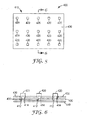
FIG. 1 is a schematic cross-sectional diagram of one illustrative thermally conductive LED assembly; -
FIG. 2 is a schematic cross-sectional diagram of another illustrative thermally conductive LED assembly; -
FIG. 3 is a schematic top view ofFIG. 1 ; -
FIG. 4 is a schematic cross-sectional diagram of another illustrative thermally conductive LED assembly; -
FIG. 5 is a schematic top view of another illustrative thermally conductive LED assembly; and -
FIG. 6 is a schematic cross-sectional view of the thermally conductive LED assembly illustrated inFIG. 5 and taken along lines 6-6. - This disclosure describes thermally conductive LED assemblies. The disclosure herein allows for enhanced operation and performance of LEDs that create a large amount of heat by allowing this heat to be removed from the local area of each LED. This heat can be removed, for example, by radiation or conduction. In this way, LEDs operating at maximum power provide maximum light output and operate to expected lifetimes. In addition, the assemblies described herein can allow for more high power LEDs to be operated along a flexible cable than with conventional wiring systems because such assemblies can dissipate heat effectively.
- Accordingly, the present disclosure is directed generally to thermally conductive LED assemblies, and particularly to thermally conductive LED assemblies that include an array of LEDs. While the present disclosure is not so limited, an appreciation of various aspects of the disclosure will be gained through a discussion of the examples provided below.
- The following description should be read with reference to the drawings, in which like elements in different drawings are numbered in like fashion. The drawings, which are not necessarily to scale, depict selected illustrative embodiments and are not intended to limit the scope of the disclosure. Although examples of construction, dimensions, and materials are illustrated for the various elements, those skilled in the art will recognize that many of the examples provided have suitable alternatives that may be utilized.
- Unless otherwise indicated, all numbers expressing feature sizes, amounts, and physical properties used in the specification and claims are to be understood as being modified in all instances by the term "about." Accordingly, unless indicated to the contrary, the numerical parameters set forth in the foregoing specification and attached claims are approximations that can vary depending upon the desired properties sought to be obtained by those skilled in the art utilizing the teachings disclosed herein.
- The recitation of numerical ranges by endpoints includes all numbers subsumed within that range (e.g. 1 to 5 includes 1, 1.5, 2, 2.75, 3, 3.80, 4, and 5) and any range within that range.
- As used in this specification and the appended claims, the singular forms "a", "an", and "the" encompass embodiments having plural referents, unless the content clearly dictates otherwise. As used in this specification and the appended claims, the term "or" is generally employed in its sense including "and/or" unless the content clearly dictates otherwise.
-
FIG. 1 is a schematic cross-sectional diagram of one illustrative thermallyconductive LED assembly 100.FIG. 3 is a schematic top view ofFIG. 1 . In many embodiments, the LED assemblies described herein are generally flexible flat cable assemblies. These flexible flat cable assemblies can be elastically deformed as desired. While the Figures show the LED generally disposed on the exterior of the flat cable, the LED may also be disposed within the flat cable such that the LED is recessed within the cable jacket any useful distance. In addition, the LED may be seated directly on the flat conductors or connected through one or more vias, as desired. In addition, the LEDs can be connected to the flat cable using any suitable technique, e.g., the techniques described inU.S. Patent Nos. 5,987,204 (Lee et al. ) and6,148,130 (Lee et al. ). The thermally conductive LED assembly can take any useful form such as a linear array of LEDs illustrated inFIG. 3 , or an two dimensional array of LEDs illustrated inFIG. 5 . The term elongate flat conductor cable refers both to the linear array of LEDs illustrated inFIG. 3 and the two dimensional array of LEDs illustrated inFIG. 5 - In some embodiments, the
assembly 100 includes an elongateflat conductor cable 110 having afirst conductor 112 and asecond conductor 114. In some embodiments, thefirst conductor 112 andsecond conductor 114 extend along a length of the elongateflat conductor cable 110 and are in side by side configuration. Although illustrated inFIG. 1 as including a flat cross-sectional shape, the first andsecond conductors flat conductor cable 110 can have any useful length L such as, for example, 0.5 to 10 meters, or from 0.5 to 3 meters, as desired. - The elongate
flat conductor cable 110 linear array can have any useful thickness T and width W. In many embodiments, the elongateflat conductor cable 110 has an aspect ratio (W/T) of greater than 2, 3, 4, 5, 6, 7, 8, 9, or 10. In some embodiments, the elongateflat conductor cable 110 can have a thickness T in a range from 0.2 to 2 mm, or from 0.5 to 1 mm, and a width W in a range from 2 to 10 mm, or from 3 to 7 mm. - The
first conductor 112 and thesecond conductor 114 can have an aspect ratio of greater than 2, 3, 4, 5, 6, 7, 8, 9, or 10. In some embodiments, thefirst conductor 112 and thesecond conductor 114 can have a thickness in a range from 0.1 to 0.5 mm, or from 0.1 to 0.3 millimeters and a width in a range from 0.2 to 2 mm, or from 0.5 to 1 mm. Thefirst conductor 112 and thesecond conductor 114 can be formed from any useful conductive material such as, for example, a metal such as copper. - A plurality of elongate
flat conductor cables 110 can be formed as a single structure or individually formed and then connected to form a single structure having a plurality of parallel elongateflat conductor cables 110. Thus, wide "mats" of parallel elongateflat conductor cables 110 can be utilized to illuminate an area as desired. Alternatively, a wide "mat" or web of elongateflat conductor cables 110 can be formed (e.g., extruded) and optionally separated along lines of weakness between the elongateflat conductor cables 110. - One or
more LEDs 120 are disposed on the elongateflat conductor cable 110, and eachLED 120 is in electrical connection with thefirst conductor 112 and thesecond conductor 114. In many embodiments, a plurality ofLEDs 120 are disposed on the elongateflat conductor cable 110 along the length of the elongateflat conductor cable 110. - "Light emitting diode" or "LED" refers to a diode that emits light, whether visible, ultraviolet, or infrared. It includes incoherent encased or encapsulated semiconductor devices marketed as "LEDs", whether of the conventional or super radiant variety, and whether of the forward-emitting or side-emitting variety, the latter of which is often advantageous in display applications. If the LED emits non-visible light such as ultraviolet light, and in some cases where it emits visible light, it can be packaged to include an organic or inorganic phosphor (or it may illuminate a remotely disposed phosphor) to convert short wavelength light to longer wavelength visible light, in some cases yielding a device that emits white light. An "LED die" is an LED in its most basic form, i.e., in the form of an individual component or chip made by semiconductor processing procedures. For example, the LED die is ordinarily formed from a combination of one or more Group III elements and of one or more Group V elements (III-V semiconductor). Examples of suitable III-V semiconductor materials include nitrides, such as gallium nitride, and phosphides, such as indium gallium phosphide. Other types of III-V materials can be used also, as might inorganic materials from other groups of the periodic table. The component or chip can include electrical contacts suitable for application of power to energize the device. The individual layers and other functional elements of the component or chip are typically formed on the wafer scale, and the finished wafer can then be diced into individual piece parts to yield a multiplicity of LED dies. The LED die may be configured for surface mount, chip-on-board, or other known mounting configurations. Some packaged LEDs are made by forming a polymer encapsulant formed over an LED die and an associated reflector cup. The LED(s) 120 can operate via DC or AC current.
- The elongate
flat conductor cable 110 includes a polymeric jacket orfilm 130 surrounding or in contact with thefirst conductor 112 and thesecond conductor 114. Thepolymeric film 130 is electrically insulating and thermally conductive. Thepolymeric film 130 can have a thermal impedance value in a range from 2.5 to 15 C°-cm2/W. In many embodiments, thepolymeric film 130 is formed from a suitable polymer and a thermally conductive and electrically insulating filler material or particles. The thermally conductive and electrically insulating filler material or particles can be present in thepolymeric film 130 in any useful amount such as, for example, 5 to 75 wt%, or from 10 to 50 wt%. Thepolymeric film 130 can be a monolithic element as illustrated inFIG. 1 or it can be a plurality of layers disposed about the first conductor and the second conductor as illustrated inFIG. 6 . - The
polymeric film 130 can include any suitable polymer or polymers, e.g., polyesters, polyurethanes, fluoropolymers, silicones and other cable jacketing materials. In some embodiments, the polymer includes polybutylene terephthalate (PBT), thermoplastic polyurethane (TPU), polyvinyl chloride (PVC), Teflon, Tefzel, and/or silicone. - Thermally conductive and electrically insulating fillers or particles include, for example, titanium dioxide, boron nitride, single walled carbon nanotubes and other inorganics. Single walled carbon nanotubes (see, e.g., M.J. Biercuk, et al., Appl. Phys. Letters, 80(15), 2767, April 2002) can offer enhanced thermal conductivity at loading levels of less than 2 wt% or less than 1 wt% or from 0.1 to 0.2 wt%.
- In some embodiments the electrically insulating and thermally conductive polymeric jacket is provided as Light Enhancement Film 3635-100 (LEF) available from 3M Company, St. Paul, Minnesota.
- A plurality of
LEDs 120 are disposed on the elongateflat conductor cable 110 along the length of the elongateflat conductor cable 110 at an interval I such that enough space remains between each LED so that the heat generated by the LED is radiated or conducted away from the LED via the thermally conductive elongateflat conductor cable 110. - In many embodiments, a light reflective layer or material can be disposed on one or more of the major surfaces of the elongate
flat conductor cable 110. In many embodiments, the light reflective layer is adjacent to the LED. In some embodiments, the light reflective layer is the electrically insulating and thermally conductivepolymeric film 130. The light reflective layer or material can be a predominantly specular, diffuse, or combination specular/diffuse reflector, whether spatially uniform or patterned. - Any suitable light reflective material or materials may be used for the reflective layer, e.g., metal, polymeric, etc. Reflective materials may be mirror films, opaque films or other materials capable of light reflection. An example of suitable high reflectivity materials include Vikuiti™ Enhanced Specular Reflector (ESR) multilayer polymeric film available from 3M Company; a film made by laminating a barium sulfate-loaded polyethylene terephthalate film (2 mils thick) to Vikuiti™ ESR film using a 0.4 mil thick isooctylacrylate acrylic acid pressure sensitive adhesive, the resulting laminate film referred to herein as "EDR II" film; E-60 series Lumirror™ polyester film available from Toray Industries, Inc.; Light Enhancement Film 3635-100 (LEF) available from 3M Company, porous polytetrafluoroethylene (PTFE) films, such as those available from W. L. Gore & Associates, Inc.; Spectralon™ reflectance material available from Labsphere, Inc.; Miro™ anodized aluminum films (including Miro™ 2 film) available from Alanod Aluminum-Veredlung GmbH & Co.; MCPET high reflectivity foamed sheeting from Furukawa Electric Co., Ltd.; and White Refstar™ films and MT films available from Mitsui Chemicals, Inc. In some embodiments, the reflective layer or material is Vikuiti™ Enhanced Specular Reflector (ESR) multilayer polymeric film available from 3M Company, St. Paul, Minnesota. The reflective surfaces can direct or distribute light emitted from the
LED 120 away from the elongateflat conductor cable 110. -
FIG. 2 is a schematic cross-sectional diagram of another illustrative thermallyconductive LED assembly 200. Theassembly 200 includes an elongateribbed conductor cable 210 having afirst conductor 212 and asecond conductor 214. Thefirst conductor 212 and thesecond conductor 214 can extend along a length of the elongateribbed conductor cable 210 and be in side by side configuration. One or more LED(s) 220 are disposed on the elongateribbed conductor cable 210 and eachLED 220 is in electrical connection with thefirst conductor 212 and thesecond conductor 214. The elongateribbed conductor cable 210 includes a polymeric film orjacket 230 surrounding thefirst conductor 212 and thesecond conductor 214. TheLED 220,first conductor 212,second conductor 214, andpolymeric jacket 230 are described above. - In this embodiment, the elongate
ribbed conductor cable 210 includes a plurality of ribs or projections extending from one or more major surfaces of the elongateribbed conductor cable 210. The ribs or projections provide increased surface area for heat to be radiated or conducted away from the LED and/or elongateribbed conductor cable 210. - The elongate
ribbed conductor cable 210 or elongateflat conductor cable 110 can be formed by any useful method such as, for example, lamination or polymer extrusion around the conductors. - A thermally conductive
adhesive layer 240 can be disposed on the elongateribbed conductor cable 210. In the illustrated embodiment, the thermally conductiveadhesive layer 240 is disposed between the elongateribbed conductor cable 210 and asubstrate 250. The thermally conductiveadhesive layer 240 can have a thermal impedance value in a range from 2.5 to 15 C°-cm2/W. The thermally conductiveadhesive layer 240 can be formed of any useful material such as, for example, polyacrylates, and epoxies. The thermally conductiveadhesive layer 240 can be utilized with any of the thermally conductive LED assemblies described herein. The thermally conductiveadhesive layer 240 can be a layer that is formed on thecable 210 or a tape that is positioned on thecable 210. Suitable tapes include thermally conductive adhesive tapes commercially available under the tradename 3M™ Thermally Conductive Adhesive Transfer Tape 8805, 8810, 8815, and 8820 available from 3M Company. - The thermally conductive
adhesive layer 240 can conduct heat to thesubstrate 250, as desired. In some embodiments, the thermally conductiveadhesive layer 240 can be a pressure sensitive adhesive. In these embodiments, the thermally conductive pressure sensitiveadhesive layer 240 can include a release layer that protects the thermally conductive pressure sensitiveadhesive layer 240 and is easily removed prior to application onto thesubstrate 250. Release liners are known in the pressure sensitive adhesive art and include, for example, silicone and fluoropolymer films. - In many embodiments, a reflective layer or material can be disposed on one or more of the surfaces of the elongate
flat conductor cable 210. The reflective surfaces can direct or distribute light emitted from theLED 220 away from the elongateflat conductor cable 210. -
FIG. 4 is a schematic cross-sectional diagram of another illustrative thermallyconductive LED assembly 300. Theassembly 300 includes an elongateflat conductor cable 310 having afirst conductor 312 and asecond conductor 314. Thefirst conductor 312 and thesecond conductor 314 can extend along a length of the elongateflat conductor cable 310 and be in side by side configuration. One or more LED(s) 320 are disposed on the elongateflat conductor cable 310, and eachLED 320 is in electrical connection with thefirst conductor 312 and thesecond conductor 314. The elongateflat conductor cable 310 includes apolymeric jacket 330 surrounding thefirst conductor 312 and thesecond conductor 314. The elongateflat conductor cable 310,LED 320,first conductor 312,second conductor 314, andpolymeric jacket 330 are described above. - In the illustrated embodiment, a
lens feature 360 encapsulates theLED 320. In some embodiments, thelens feature 360 encapsulates the one ormore LED 320 and at least a portion of the elongateflat conductor cable 310. In some embodiments, thelens feature 360 can be formed of any useful material that is thermally conductive and transparent to the light emitted by theLED 320. In many embodiments, thelens feature 360 is formed from a polymer and a thermally conductive filler, as described above. In one embodiment, thelens feature 360 is formed from a transparent polyurethane polymer and a thermally conductive filler such as, for example, single walled carbon nanotubes. - In many embodiments, a reflective layer or material can be disposed on one or more of the surfaces of the of the elongate
flat conductor cable 310. The reflective surfaces can direct or distribute light emitted from theLED 320 away from the elongateflat conductor cable 310. -
FIG. 5 is a schematic top view of another illustrative thermallyconductive LED assembly 400 andFIG. 6 is a schematic cross-sectional view of the thermallyconductive LED assembly 400 illustrated inFIG. 5 and taken along lines 6-6. In these embodiments, the thermallyconductive LED assembly 400 is illustrated as a two dimensional array having a uniform pattern ofLEDs 420, however, it is understood that the thermallyconductive LED assembly 400 can be a two dimensional array having a non-uniform pattern ofLEDs 420. These thermallyconductive LED assemblies 400 can be described as illumination mats or films that are often flexible. - The
assembly 400 includes an elongateflat conductor cable 410 having a first conductor patternedgrid layer 412 and a corresponding second conductor patternedgrid layer 414. In many embodiments, the first conductor patternedgrid layer 412 and the first conductor patternedgrid layer 414 extend along a length and/or width of the elongateflat conductor cable 410. An electrically insulating and thermally conductingpolymeric film 430 is disposed on and/or between the first conductor patternedgrid layer 412 and the first conductor patternedgrid layer 414. Thepolymeric film 430 is electrically insulating and thermally conductive, as described above. In many embodiments, thepolymeric film 430 is disposed about the first conductor patternedgrid layer 412 and the first conductor patternedgrid layer 414 aslayers 430. In some embodiments, a thermally conductiveadhesive layer 440 is disposed on the elongateflat conductor cable 410, as described above. - In many embodiments, the first conductor patterned
grid layer 412 and second conductor patternedgrid layer 414 may be formed by a electrically conductive sheet such as copper or aluminum foil, for example, that may be continuous or patterned, for example by rotary die cutting, laser patterning, water jet cutting, or other cutting ways commercially available. These conductivepatterned layers polymeric film 430, or alternately, be positioned and secured between electrically insulating and thermally conductingpolymeric films 430 and then bonded together. Circuit configurations may include busses in a grid pattern, or any other desired pattern. - In many embodiments, a light reflective layer or material can be disposed on one or more of the major surfaces of the assembly. In many embodiments, the light reflective layer is adjacent to the LED. In some embodiments, the light reflective layer is the electrically insulating and thermally conductive polymeric film. The light reflective layer or material can be a predominantly specular, diffuse, or combination specular/diffuse reflector, whether spatially uniform or patterned. The light reflective layer can be formed of any useful material, as described above.
- The
assembly 400 is a two dimensional array of LEDs (in the form of a film) that can have any useful thickness T and width W. In many embodiments, the elongateflat conductor cable 400 has a film-like aspect ratio (W/T) of greater than 25, 50, 100, 250, 500, 1000, 2000, 5000, or 10000. In some embodiments, the elongateflat conductor cable 400 can have a thickness T in a range from 0.1 to 5 mm, or from 0.2 to 3 mm, or from 0.5 to 2 mm, and a width W in a range from 25 to 3000 mm, or from 250 to 3000 mm, or a width of greater than 3000 mm. - This thermally
conductive LED assembly 400 can be formed by any useful method such as a roll-to-roll process as described in U.S. Patent application No. (Attorney docket No. 62995US002) filed on even date herewith and incorporated by reference. - Knowing the thermal impedance, conductor width and the like, of the LED assembly allows a user to place particularly sized LEDs onto the elongate flat conductor cable at an interval or pitch so that the heat emitted from the LED can be dissipated from the LED assembly without reducing the efficiency of the LEDs.
- Illustrative embodiments of this disclosure are discussed and reference has been made to possible variations within the scope of this disclosure. These and other variations and modifications in the disclosure will be apparent to those skilled in the art without departing from the scope of the disclosure, and it should be understood that this disclosure is not limited to the illustrative embodiments set forth herein. Accordingly, the disclosure is to be limited only by the claims provided below.
Claims (14)
- A thermally conductive LED assembly, comprising:an elongate conductor cable having a first conductor and a second conductor extending along a length of the elongate conductor cable and a first thermally conducting and electrically insulating polymer layer disposed between first conductor and second conductor and a second electrically insulating polymer layer is disposed on the first conductor or second conductor, and the first electrically insulating polymer layer having a thermal impedance value in a range from 2.5 to 15 C°-cm2/W; anda plurality of light emitting diodes disposed along the length of the elongate conductor cable and each light emitting diode being in electrical connection with the first conductor and the second conductor.
- A thermally conductive LED assembly according to claim 1, wherein the elongate conductor cable has a thickness and a width and a width/thickness aspect ratio of greater than 5.
- A thermally conductive LED assembly according to claim 1, wherein the plurality of light emitting diodes are disposed along the length and a width of the elongate conductor cable, forming a two dimensional array of light emitting diodes.
- A thermally conductive LED assembly according to claim 1, wherein the first conductor or second conductor is a patterned grid layer.
- A thermally conductive LED assembly according to claim 1, wherein the elongate conductor cable has projections or fins extending away from a major surface of the elongate conductor cable.
- A thermally conductive LED assembly according to claim 1, wherein the first conductor and second conductor are patterned grid layers.
- A thermally conductive LED assembly according to claim 1, wherein the elongate conductor cable comprises thermally conducting particles dispersed in a polymeric binder.
- A thermally conductive LED assembly according to claim 1, wherein the elongate conductor cable comprises thermally conducting single walled carbon nanotubes dispersed in a polymeric binder.
- A thermally conductive LED assembly according to claim 1, further comprising a light reflective layer disposed on a major surface of the elongate conductor cable.
- A thermally conductive LED assembly according to claim 1, wherein the elongate conductor cable comprises a lens disposed on the plurality of LEDs.
- A thermally conductive LED assembly according to claim 1, further comprising a thermally conductive adhesive layer disposed on the elongate conductor cable and the thermally conductive adhesive layer has a thermal impedance value in a range from 2.5 to 15 C°-cm2/W.
- A method of forming a thermally conductive LED assembly, comprising:disposing a first thermally conductive and electrically insulating polymer layer between a first conductor and second conductor and disposing a second electrically insulating polymer layer on the first conductor or second conductor to form a length of an elongate conductor cable, the first electrically insulating polymer layer having a thermal impedance value in a range from 2.5 to 15 C°-cm2/W; andplacing a plurality of LEDs on the length of elongate conductor cable, wherein each LED is in electrical connection with the first conductor and the second conductor to form a thermally conductive LED assembly.
- The method according to claim 12, wherein the placing step comprises placing a plurality of LEDs along the length and a width of the elongate conductor cable, forming a two dimensional array of light emitting diodes.
- The method according to claim 12, wherein disposing step comprises disposing a thermally conductive and electrically insulating polymer layer between a first conductor patterned grid layer and a second conductor patterned grid layer to form a length of an elongate conductor cable.
Applications Claiming Priority (3)
| Application Number | Priority Date | Filing Date | Title |
|---|---|---|---|
| US82645706P | 2006-09-21 | 2006-09-21 | |
| US11/756,929 US8581393B2 (en) | 2006-09-21 | 2007-06-01 | Thermally conductive LED assembly |
| PCT/US2007/078473 WO2008036560A1 (en) | 2006-09-21 | 2007-09-14 | Thermally conductive led assembly |
Publications (3)
| Publication Number | Publication Date |
|---|---|
| EP2082440A1 EP2082440A1 (en) | 2009-07-29 |
| EP2082440A4 EP2082440A4 (en) | 2013-05-01 |
| EP2082440B1 true EP2082440B1 (en) | 2014-04-16 |
Family
ID=39200825
Family Applications (1)
| Application Number | Title | Priority Date | Filing Date |
|---|---|---|---|
| EP07842482.7A Not-in-force EP2082440B1 (en) | 2006-09-21 | 2007-09-14 | Thermally conductive led assembly |
Country Status (5)
| Country | Link |
|---|---|
| US (2) | US8581393B2 (en) |
| EP (1) | EP2082440B1 (en) |
| JP (1) | JP5357034B2 (en) |
| KR (1) | KR101422873B1 (en) |
| WO (1) | WO2008036560A1 (en) |
Families Citing this family (27)
| Publication number | Priority date | Publication date | Assignee | Title |
|---|---|---|---|---|
| US10340424B2 (en) | 2002-08-30 | 2019-07-02 | GE Lighting Solutions, LLC | Light emitting diode component |
| WO2006098799A2 (en) * | 2005-03-12 | 2006-09-21 | 3M Innovative Properties Company | Illumination devices and methods for making the same |
| US8525402B2 (en) * | 2006-09-11 | 2013-09-03 | 3M Innovative Properties Company | Illumination devices and methods for making the same |
| US20080295327A1 (en) * | 2007-06-01 | 2008-12-04 | 3M Innovative Properties Company | Flexible circuit |
| US7717591B2 (en) * | 2007-12-27 | 2010-05-18 | Lumination Llc | Incorporating reflective layers into LED systems and/or components |
| US8092044B1 (en) * | 2008-11-21 | 2012-01-10 | Tomar Electronics, Inc. | LED light assembly and related methods |
| US8593040B2 (en) | 2009-10-02 | 2013-11-26 | Ge Lighting Solutions Llc | LED lamp with surface area enhancing fins |
| US8408627B2 (en) * | 2009-12-15 | 2013-04-02 | 3M Innovative Properties Company | Pick up truck, rail cap assembly with lighting system and method of use |
| US8541933B2 (en) * | 2010-01-12 | 2013-09-24 | GE Lighting Solutions, LLC | Transparent thermally conductive polymer composites for light source thermal management |
| JP2013524439A (en) * | 2010-04-02 | 2013-06-17 | ジーイー ライティング ソリューションズ エルエルシー | Light weight heat sink and LED lamp using the same |
| US10240772B2 (en) * | 2010-04-02 | 2019-03-26 | GE Lighting Solutions, LLC | Lightweight heat sinks and LED lamps employing same |
| US8668356B2 (en) * | 2010-04-02 | 2014-03-11 | GE Lighting Solutions, LLC | Lightweight heat sinks and LED lamps employing same |
| KR20120032871A (en) * | 2010-09-29 | 2012-04-06 | 삼성전기주식회사 | Radiating substrate and method for manufacturing the radiating substrate, and luminous element package with the radiating structure |
| US8597988B2 (en) * | 2010-11-18 | 2013-12-03 | Bridgelux, Inc. | System for flash-free overmolding of led array substrates |
| NO2699839T3 (en) * | 2011-04-18 | 2018-05-19 | ||
| WO2013030714A1 (en) | 2011-08-29 | 2013-03-07 | Koninklijke Philips Electronics N.V. | A flexible lighting assembly, a luminaire, and a method of manufacturing a flexible layer |
| KR101260007B1 (en) | 2011-09-27 | 2013-05-06 | 주식회사 솔고 바이오메디칼 | Glasses having a warming function |
| US9874316B2 (en) | 2012-01-03 | 2018-01-23 | Philips Lighting Holding B.V. | Lighting assembly, a light source and a luminaire |
| US9500355B2 (en) | 2012-05-04 | 2016-11-22 | GE Lighting Solutions, LLC | Lamp with light emitting elements surrounding active cooling device |
| US10156352B2 (en) * | 2013-04-19 | 2018-12-18 | Covestro Llc | In mold electronic printed circuit board encapsulation and assembly |
| EP3014657B1 (en) | 2013-06-28 | 2018-04-25 | Lumileds Holding B.V. | Led dies bonded to lead frame strips |
| US9379289B1 (en) * | 2013-10-30 | 2016-06-28 | Automated Assembly Corporation | LEDs on adhesive transfer tape |
| US9897292B1 (en) | 2013-10-30 | 2018-02-20 | Automated Assembly Corporation | Solid-state lighting elements on adhesive transfer tape |
| EP3143647A4 (en) * | 2014-05-15 | 2017-09-27 | 3M Innovative Properties Company | Flexible circuit on reflective substrate |
| US9989223B1 (en) | 2015-03-09 | 2018-06-05 | Automated Assembly Corporation | LED lighting apparatus with LEDs and wires attached to metal sheet member by adhesive |
| CN109155349B (en) * | 2016-05-18 | 2021-09-07 | 亮锐控股有限公司 | Lighting assembly and method for manufacturing a lighting assembly |
| US10168037B1 (en) | 2016-06-02 | 2019-01-01 | Automated Assembly Corporation | SSL lighting apparatus |
Family Cites Families (154)
| Publication number | Priority date | Publication date | Assignee | Title |
|---|---|---|---|---|
| US3589324A (en) * | 1969-12-02 | 1971-06-29 | Schuyler V V Hoffman | Roll stabilizer for boats |
| JPS5555556A (en) | 1978-09-29 | 1980-04-23 | Hakutou Kk | Device for adhering non-conductivity tape having plating hole to metallic tape blank |
| US4271408A (en) | 1978-10-17 | 1981-06-02 | Stanley Electric Co., Ltd. | Colored-light emitting display |
| US4502761A (en) | 1981-03-13 | 1985-03-05 | Robert Bosch Gmbh | Gradient-free illumination of passive readout display devices |
| US4409981A (en) | 1981-07-20 | 1983-10-18 | Minnesota Mining And Manufacturing Company | Medical electrode |
| US4542449A (en) | 1983-08-29 | 1985-09-17 | Canadian Patents & Development Limited | Lighting panel with opposed 45° corrugations |
| US4588258A (en) | 1983-09-12 | 1986-05-13 | Minnesota Mining And Manufacturing Company | Cube-corner retroreflective articles having wide angularity in multiple viewing planes |
| DK163151C (en) | 1983-11-16 | 1992-06-22 | Minnesota Mining & Mfg | LABEL PLATE WITH LC RESONANCE CIRCUIT FOR USE IN ELECTRONIC OBJECT MONITORING SYSTEM, METHOD FOR MANUFACTURING BOTTLE PLATES, AND ELECTRONIC OBJECT MONITORING SYSTEM THEREOF. |
| CA1319341C (en) | 1985-03-29 | 1993-06-22 | Frederick J. Fox | Method of supporting a louvered plastic film |
| US5056892A (en) | 1985-11-21 | 1991-10-15 | Minnesota Mining And Manufacturing Company | Totally internally reflecting thin, flexible film |
| US4782893A (en) | 1986-09-15 | 1988-11-08 | Trique Concepts, Inc. | Electrically insulating thermally conductive pad for mounting electronic components |
| US4846922A (en) | 1986-09-29 | 1989-07-11 | Monarch Marking Systems, Inc. | Method of making deactivatable tags |
| US4721408A (en) * | 1986-10-22 | 1988-01-26 | Hewlett Robert F | Water distribution system |
| US4775219A (en) | 1986-11-21 | 1988-10-04 | Minnesota Mining & Manufacturing Company | Cube-corner retroreflective articles having tailored divergence profiles |
| US4766023A (en) | 1987-01-16 | 1988-08-23 | Minnesota Mining And Manufacturing Company | Method for making a flexible louvered plastic film with protective coatings and film produced thereby |
| CA1278203C (en) | 1987-04-24 | 1990-12-27 | Lorne A. Whitehead | Non-reflective image display device |
| US4984144A (en) | 1987-05-08 | 1991-01-08 | Minnesota Mining And Manufacturing Company | High aspect ratio light fixture and film for use therein |
| US4791540A (en) | 1987-05-26 | 1988-12-13 | Minnesota Mining And Manufacturing Company | Light fixture providing normalized output |
| US4799131A (en) | 1987-11-18 | 1989-01-17 | Minnesota Mining And Manufacturing Company | Automotive lighting element |
| US5175030A (en) | 1989-02-10 | 1992-12-29 | Minnesota Mining And Manufacturing Company | Microstructure-bearing composite plastic articles and method of making |
| US5183597A (en) | 1989-02-10 | 1993-02-02 | Minnesota Mining And Manufacturing Company | Method of molding microstructure bearing composite plastic articles |
| US5122902A (en) | 1989-03-31 | 1992-06-16 | Minnesota Mining And Manufacturing Company | Retroreflective articles having light-transmissive surfaces |
| US5122905A (en) | 1989-06-20 | 1992-06-16 | The Dow Chemical Company | Relective polymeric body |
| US5486949A (en) | 1989-06-20 | 1996-01-23 | The Dow Chemical Company | Birefringent interference polarizer |
| US5161041A (en) | 1990-04-26 | 1992-11-03 | Ois Optical Imaging Systems, Inc. | Lighting assembly for a backlit electronic display including an integral image splitting and collimating means |
| US5138488A (en) | 1990-09-10 | 1992-08-11 | Minnesota Mining And Manufacturing Company | Retroreflective material with improved angularity |
| US5254388A (en) | 1990-12-21 | 1993-10-19 | Minnesota Mining And Manufacturing Company | Light control film with reduced ghost images |
| US5094788A (en) | 1990-12-21 | 1992-03-10 | The Dow Chemical Company | Interfacial surface generator |
| US5217794A (en) | 1991-01-22 | 1993-06-08 | The Dow Chemical Company | Lamellar polymeric body |
| US5248193A (en) | 1991-10-18 | 1993-09-28 | Texas Microsystems, Inc. | Extruded enclosure for a computer system |
| US5303322A (en) | 1992-03-23 | 1994-04-12 | Nioptics Corporation | Tapered multilayer luminaire devices |
| US5528720A (en) | 1992-03-23 | 1996-06-18 | Minnesota Mining And Manufacturing Co. | Tapered multilayer luminaire devices |
| US5269995A (en) | 1992-10-02 | 1993-12-14 | The Dow Chemical Company | Coextrusion of multilayer articles using protective boundary layers and apparatus therefor |
| US5321593A (en) * | 1992-10-27 | 1994-06-14 | Moates Martin G | Strip lighting system using light emitting diodes |
| US5353154A (en) | 1992-11-02 | 1994-10-04 | The Dow Chemical Company | Polymeric reflective materials utilizing a back light source |
| TW289095B (en) | 1993-01-11 | 1996-10-21 | ||
| US6052164A (en) | 1993-03-01 | 2000-04-18 | 3M Innovative Properties Company | Electroluminescent display with brightness enhancement |
| US5310355A (en) | 1993-03-09 | 1994-05-10 | Irmgard Dannatt | Strip lighting assembly |
| US5389324A (en) | 1993-06-07 | 1995-02-14 | The Dow Chemical Company | Layer thickness gradient control in multilayer polymeric bodies |
| DE4340996C1 (en) | 1993-12-02 | 1995-03-02 | Heraeus Gmbh W C | Method and device for producing a film laminate |
| US5882774A (en) | 1993-12-21 | 1999-03-16 | Minnesota Mining And Manufacturing Company | Optical film |
| US6025897A (en) | 1993-12-21 | 2000-02-15 | 3M Innovative Properties Co. | Display with reflective polarizer and randomizing cavity |
| US5828488A (en) | 1993-12-21 | 1998-10-27 | Minnesota Mining And Manufacturing Co. | Reflective polarizer display |
| EP0665705B1 (en) | 1993-12-30 | 2009-08-19 | Kabushiki Kaisha Miyake | Circuit-like metallic foil sheet and the like and process for producing them |
| US6101032A (en) | 1994-04-06 | 2000-08-08 | 3M Innovative Properties Company | Light fixture having a multilayer polymeric film |
| CA2190969C (en) | 1994-06-21 | 2003-05-27 | Andrew J. Ouderkirk | A composite used for light control or privacy |
| DE69532771T2 (en) | 1994-09-27 | 2004-09-30 | Minnesota Mining And Mfg. Co., St. Paul | Luminance control film |
| US6458465B1 (en) | 1994-12-30 | 2002-10-01 | Kabushiki Kaisha Miyake | Circuit-like metallic foil sheet and the like and process for producing them |
| US5626800A (en) | 1995-02-03 | 1997-05-06 | Minnesota Mining And Manufacturing Company | Prevention of groove tip deformation in brightness enhancement film |
| KR100398940B1 (en) | 1995-03-03 | 2003-12-31 | 미네소타 마이닝 앤드 매뉴팩춰링 캄파니 | A light directing film having a structure screen of various heights and an article comprising such a film |
| US5751388A (en) | 1995-04-07 | 1998-05-12 | Honeywell Inc. | High efficiency polarized display |
| KR100454834B1 (en) | 1995-06-26 | 2005-06-17 | 미네소타 마이닝 앤드 매뉴팩춰링 캄파니 | Light Diffusing Adhesive |
| US5699188A (en) | 1995-06-26 | 1997-12-16 | Minnesota Mining And Manufacturing Co. | Metal-coated multilayer mirror |
| US6080467A (en) | 1995-06-26 | 2000-06-27 | 3M Innovative Properties Company | High efficiency optical devices |
| US6088067A (en) | 1995-06-26 | 2000-07-11 | 3M Innovative Properties Company | Liquid crystal display projection system using multilayer optical film polarizers |
| AU706253B2 (en) | 1995-06-26 | 1999-06-10 | Minnesota Mining And Manufacturing Company | Transflective displays with reflective polarizing transflector |
| EP0855043B1 (en) | 1995-06-26 | 2003-02-05 | Minnesota Mining And Manufacturing Company | Diffusely reflecting multilayer polarizers and mirrors |
| US5703664A (en) | 1995-10-23 | 1997-12-30 | Motorola, Inc. | Integrated electro-optic package for reflective spatial light modulators |
| IT1284335B1 (en) | 1996-01-24 | 1998-05-18 | Fiat Ricerche | DEVICES WITH MICRO-MIRRORS AND MICROFILTERS FOR THE SELECTION OF COLORS AND IMAGES |
| US5917664A (en) | 1996-02-05 | 1999-06-29 | 3M Innovative Properties Company | Brightness enhancement film with soft cutoff |
| US5759422A (en) | 1996-02-14 | 1998-06-02 | Fort James Corporation | Patterned metal foil laminate and method for making same |
| US5825543A (en) | 1996-02-29 | 1998-10-20 | Minnesota Mining And Manufacturing Company | Diffusely reflecting polarizing element including a first birefringent phase and a second phase |
| US5867316A (en) | 1996-02-29 | 1999-02-02 | Minnesota Mining And Manufacturing Company | Multilayer film having a continuous and disperse phase |
| US5783120A (en) | 1996-02-29 | 1998-07-21 | Minnesota Mining And Manufacturing Company | Method for making an optical film |
| US5919551A (en) | 1996-04-12 | 1999-07-06 | 3M Innovative Properties Company | Variable pitch structured optical film |
| US5840405A (en) | 1996-04-30 | 1998-11-24 | Minnesota Mining And Manufacturing Company | Glittering cube-corner retroreflective sheeting |
| US5753976A (en) | 1996-06-14 | 1998-05-19 | Minnesota Mining And Manufacturing Company | Multi-layer circuit having a via matrix interlayer connection |
| EP1249354A1 (en) * | 1996-06-14 | 2002-10-16 | Minnesota Mining And Manufacturing Company | Display unit and methods of displaying an image |
| US5908874A (en) | 1996-06-18 | 1999-06-01 | 3M Innovative Properties Company | Polymerizable compositions containing fluorochemicals to reduce melting temperature |
| US5808794A (en) | 1996-07-31 | 1998-09-15 | Weber; Michael F. | Reflective polarizers having extended red band edge for controlled off axis color |
| US5976424A (en) | 1996-07-31 | 1999-11-02 | Minnesota Mining And Manufacturing Company | Method for making multilayer optical films having thin optical layers |
| FR2752640B1 (en) | 1996-08-21 | 1998-11-06 | Jolly Andre Jean | METHOD FOR MANUFACTURING A SANDWICH PANEL WITH HIGH RESILIENCE CONDUCTIVE CORES AND PANEL OBTAINED |
| JPH1075053A (en) | 1996-09-02 | 1998-03-17 | Mitsui Petrochem Ind Ltd | Method for manufacturing flexible metal foil laminated board |
| US5857767A (en) * | 1996-09-23 | 1999-01-12 | Relume Corporation | Thermal management system for L.E.D. arrays |
| JPH10286911A (en) * | 1997-04-14 | 1998-10-27 | Nippon Zeon Co Ltd | Laminate |
| US6280063B1 (en) | 1997-05-09 | 2001-08-28 | 3M Innovative Properties Company | Brightness enhancement article |
| US5987204A (en) | 1997-10-14 | 1999-11-16 | 3M Innnvative Properties Company | Cable with predetermined discrete connectorization locations |
| TW408497B (en) | 1997-11-25 | 2000-10-11 | Matsushita Electric Works Ltd | LED illuminating apparatus |
| US6157490A (en) | 1998-01-13 | 2000-12-05 | 3M Innovative Properties Company | Optical film with sharpened bandedge |
| US6179948B1 (en) | 1998-01-13 | 2001-01-30 | 3M Innovative Properties Company | Optical film and process for manufacture thereof |
| US6618939B2 (en) | 1998-02-27 | 2003-09-16 | Kabushiki Kaisha Miyake | Process for producing resonant tag |
| US6140707A (en) | 1998-05-07 | 2000-10-31 | 3M Innovative Properties Co. | Laminated integrated circuit package |
| US6256146B1 (en) | 1998-07-31 | 2001-07-03 | 3M Innovative Properties | Post-forming continuous/disperse phase optical bodies |
| US6005713A (en) | 1998-08-21 | 1999-12-21 | 3M Innovative Properties Company | Multilayer polarizer having a continuous and disperse phase |
| US6246010B1 (en) | 1998-11-25 | 2001-06-12 | 3M Innovative Properties Company | High density electronic package |
| US6208466B1 (en) | 1998-11-25 | 2001-03-27 | 3M Innovative Properties Company | Multilayer reflector with selective transmission |
| JP3405242B2 (en) | 1998-12-21 | 2003-05-12 | ソニーケミカル株式会社 | Flexible board |
| US6280822B1 (en) | 1999-01-11 | 2001-08-28 | 3M Innovative Properties Company | Cube corner cavity based retroeflectors with transparent fill material |
| US6287670B1 (en) | 1999-01-11 | 2001-09-11 | 3M Innovative Properties Company | Cube corner cavity based retroreflectors and methods for making same |
| US6752505B2 (en) | 1999-02-23 | 2004-06-22 | Solid State Opto Limited | Light redirecting films and film systems |
| US6268070B1 (en) | 1999-03-12 | 2001-07-31 | Gould Electronics Inc. | Laminate for multi-layer printed circuit |
| US6122103A (en) | 1999-06-22 | 2000-09-19 | Moxtech | Broadband wire grid polarizer for the visible spectrum |
| WO2001040357A1 (en) | 1999-12-03 | 2001-06-07 | Toray Industries, Inc. | Biaxially stretched polyester film for forming |
| JP2001284504A (en) * | 2000-03-30 | 2001-10-12 | Three M Innovative Properties Co | Heat-conductive sheet and peel film therefor |
| JP2001291807A (en) * | 2000-04-10 | 2001-10-19 | Three M Innovative Properties Co | Thermo-conductive sheet |
| JP4349600B2 (en) | 2000-04-20 | 2009-10-21 | 大日本印刷株式会社 | LAMINATE, INSULATION FILM, ELECTRONIC CIRCUIT, AND METHOD FOR PRODUCING LAMINATE |
| JP3975476B2 (en) * | 2000-09-11 | 2007-09-12 | ソニー株式会社 | Broadcasting method, broadcasting system, and content organization supply center |
| TWI295966B (en) | 2000-10-27 | 2008-04-21 | Kaneka Corp | |
| US6585846B1 (en) | 2000-11-22 | 2003-07-01 | 3M Innovative Properties Company | Rotary converting apparatus and method for laminated products and packaging |
| US6917399B2 (en) | 2001-02-22 | 2005-07-12 | 3M Innovative Properties Company | Optical bodies containing cholesteric liquid crystal material and methods of manufacture |
| DE10122324A1 (en) | 2001-05-08 | 2002-11-14 | Philips Corp Intellectual Pty | Flexible integrated monolithic circuit |
| JP2003036708A (en) | 2001-07-19 | 2003-02-07 | Ichikoh Ind Ltd | Stop lamp for automobile |
| US20030035231A1 (en) | 2001-08-03 | 2003-02-20 | Epstein Kenneth A. | Optical film having microreplicated structures; and methods |
| JP3989794B2 (en) * | 2001-08-09 | 2007-10-10 | 松下電器産業株式会社 | LED illumination device and LED illumination light source |
| CN1464953A (en) | 2001-08-09 | 2003-12-31 | 松下电器产业株式会社 | Led illuminator and card type led illuminating light source |
| US6988666B2 (en) | 2001-09-17 | 2006-01-24 | Checkpoint Systems, Inc. | Security tag and process for making same |
| US6932495B2 (en) * | 2001-10-01 | 2005-08-23 | Sloanled, Inc. | Channel letter lighting using light emitting diodes |
| TW558622B (en) | 2002-01-24 | 2003-10-21 | Yuan Lin | Lamp on sheet and manufacturing method thereof |
| US7101729B2 (en) * | 2002-03-28 | 2006-09-05 | Seiko Epson Corporation | Method of manufacturing a semiconductor device having adjoining substrates |
| US7144830B2 (en) | 2002-05-10 | 2006-12-05 | Sarnoff Corporation | Plural layer woven electronic textile, article and method |
| US6916544B2 (en) | 2002-05-17 | 2005-07-12 | E. I. Du Pont De Nemours And Company | Laminate type materials for flexible circuits or similar-type assemblies and methods relating thereto |
| US6771021B2 (en) | 2002-05-28 | 2004-08-03 | Eastman Kodak Company | Lighting apparatus with flexible OLED area illumination light source and fixture |
| TWI298988B (en) | 2002-07-19 | 2008-07-11 | Ube Industries | Copper-clad laminate |
| JP3923867B2 (en) | 2002-07-26 | 2007-06-06 | 株式会社アドバンスト・ディスプレイ | Planar light source device and liquid crystal display device using the same |
| US6776496B2 (en) | 2002-08-19 | 2004-08-17 | Eastman Kodak Company | Area illumination lighting apparatus having OLED planar light source |
| US6880954B2 (en) * | 2002-11-08 | 2005-04-19 | Smd Software, Inc. | High intensity photocuring system |
| US7557781B2 (en) | 2003-01-06 | 2009-07-07 | Tpo Displays Corp. | Planar display structure with LED light source |
| DE10308890A1 (en) | 2003-02-28 | 2004-09-09 | Opto Tech Corporation | A housing structure with a substrate, two electrodes, and a transparent insulated carrier with a depression useful for light emitting diodes |
| US6855404B2 (en) | 2003-03-13 | 2005-02-15 | E. I. Du Pont De Nemours And Company | Inorganic sheet laminate |
| JP2004304041A (en) | 2003-03-31 | 2004-10-28 | Citizen Electronics Co Ltd | Light emitting diode |
| US7013965B2 (en) | 2003-04-29 | 2006-03-21 | General Electric Company | Organic matrices containing nanomaterials to enhance bulk thermal conductivity |
| US6788541B1 (en) | 2003-05-07 | 2004-09-07 | Bear Hsiung | LED matrix moldule |
| US7128442B2 (en) | 2003-05-09 | 2006-10-31 | Kian Shin Lee | Illumination unit with a solid-state light generating source, a flexible substrate, and a flexible and optically transparent encapsulant |
| TWI321248B (en) | 2003-05-12 | 2010-03-01 | Au Optronics Corp | Led backlight module |
| US6974229B2 (en) | 2003-05-21 | 2005-12-13 | Lumileds Lighting U.S., Llc | Devices for creating brightness profiles |
| US7000999B2 (en) | 2003-06-12 | 2006-02-21 | Ryan Jr Patrick Henry | Light emitting module |
| US20050116235A1 (en) * | 2003-12-02 | 2005-06-02 | Schultz John C. | Illumination assembly |
| JP2005164952A (en) * | 2003-12-02 | 2005-06-23 | Fujisaki Denki Kk | Lighting device and power supply device for light emitting diode |
| KR100857790B1 (en) * | 2003-12-16 | 2008-09-09 | 엘지전자 주식회사 | Light emitting diode lighting apparatus and package therefor and manufacturing method for making the same |
| DE20319650U1 (en) | 2003-12-19 | 2004-04-01 | Kramer, Steffen | Flexible array of LEDs for creating illuminating surfaces by cutting circuit board into shape as needed |
| JP4668532B2 (en) * | 2003-12-26 | 2011-04-13 | 株式会社平和 | Pachinko machine |
| US7119685B2 (en) | 2004-02-23 | 2006-10-10 | Checkpoint Systems, Inc. | Method for aligning capacitor plates in a security tag and a capacitor formed thereby |
| US7138919B2 (en) | 2004-02-23 | 2006-11-21 | Checkpoint Systems, Inc. | Identification marking and method for applying the identification marking to an item |
| US7116227B2 (en) | 2004-02-23 | 2006-10-03 | Checkpoint Systems, Inc. | Tag having patterned circuit elements and a process for making same |
| JP2005249942A (en) | 2004-03-02 | 2005-09-15 | Hitachi Displays Ltd | Display device |
| KR20050090203A (en) | 2004-03-08 | 2005-09-13 | 삼성전자주식회사 | Optical member, back light assembly having the same and display device having the same |
| US20050207156A1 (en) | 2004-03-22 | 2005-09-22 | Harvatek Corporation | Flexible light array and fabrication procedure thereof |
| JP4754850B2 (en) * | 2004-03-26 | 2011-08-24 | パナソニック株式会社 | Manufacturing method of LED mounting module and manufacturing method of LED module |
| US7052924B2 (en) | 2004-03-29 | 2006-05-30 | Articulated Technologies, Llc | Light active sheet and methods for making the same |
| US7427782B2 (en) | 2004-03-29 | 2008-09-23 | Articulated Technologies, Llc | Roll-to-roll fabricated light sheet and encapsulated semiconductor circuit devices |
| US7186015B2 (en) | 2004-04-16 | 2007-03-06 | Polymore Circuit Technologies, Inc. | Backlight display system |
| JP2006100397A (en) * | 2004-09-28 | 2006-04-13 | Seiko Epson Corp | Method of manufacturing multilayered wiring board, and electronic apparatus |
| US7303315B2 (en) * | 2004-11-05 | 2007-12-04 | 3M Innovative Properties Company | Illumination assembly using circuitized strips |
| KR100674831B1 (en) * | 2004-11-05 | 2007-01-25 | 삼성전기주식회사 | White light emitting diode package and method of producing the same |
| JP4925296B2 (en) * | 2004-12-28 | 2012-04-25 | パナソニック株式会社 | Method for manufacturing high thermal conductivity circuit module and high thermal conductivity circuit module |
| US8305225B2 (en) * | 2005-02-14 | 2012-11-06 | Truck-Lite Co., Llc | LED strip light lamp assembly |
| WO2006098799A2 (en) | 2005-03-12 | 2006-09-21 | 3M Innovative Properties Company | Illumination devices and methods for making the same |
| US20060217690A1 (en) | 2005-03-22 | 2006-09-28 | Bastin Norman J | Method for treating various dermatological and muscular conditions using electromagnetic radiation |
| WO2007006147A1 (en) | 2005-07-14 | 2007-01-18 | Tir Systems Ltd. | Power board and plug-in lighting module |
| US7710045B2 (en) * | 2006-03-17 | 2010-05-04 | 3M Innovative Properties Company | Illumination assembly with enhanced thermal conductivity |
| DE202006006889U1 (en) | 2006-04-26 | 2006-08-24 | Sommer Licht- Und Werbesysteme Gmbh | Light box for presentation of translucent printed foils, has light source arranged in inner area of housing, where source is designed as circuit board with number of light emitting diodes |
| EP2049365B1 (en) | 2006-08-01 | 2017-12-13 | 3M Innovative Properties Company | Illumination device |
| US8525402B2 (en) | 2006-09-11 | 2013-09-03 | 3M Innovative Properties Company | Illumination devices and methods for making the same |
| US20080295327A1 (en) | 2007-06-01 | 2008-12-04 | 3M Innovative Properties Company | Flexible circuit |
-
2007
- 2007-06-01 US US11/756,929 patent/US8581393B2/en not_active Expired - Fee Related
- 2007-09-14 KR KR1020097007347A patent/KR101422873B1/en not_active IP Right Cessation
- 2007-09-14 WO PCT/US2007/078473 patent/WO2008036560A1/en active Application Filing
- 2007-09-14 EP EP07842482.7A patent/EP2082440B1/en not_active Not-in-force
- 2007-09-14 JP JP2009529311A patent/JP5357034B2/en not_active Expired - Fee Related
-
2013
- 2013-10-03 US US14/045,232 patent/US20140028174A1/en not_active Abandoned
Also Published As
| Publication number | Publication date |
|---|---|
| WO2008036560A1 (en) | 2008-03-27 |
| US20140028174A1 (en) | 2014-01-30 |
| KR101422873B1 (en) | 2014-07-23 |
| US20080074871A1 (en) | 2008-03-27 |
| KR20090057111A (en) | 2009-06-03 |
| JP2010504645A (en) | 2010-02-12 |
| EP2082440A1 (en) | 2009-07-29 |
| JP5357034B2 (en) | 2013-12-04 |
| US8581393B2 (en) | 2013-11-12 |
| EP2082440A4 (en) | 2013-05-01 |
Similar Documents
| Publication | Publication Date | Title |
|---|---|---|
| EP2082440B1 (en) | Thermally conductive led assembly | |
| KR101934075B1 (en) | Film system for led applications | |
| EP1810348B1 (en) | Illumination device | |
| US7236366B2 (en) | High brightness LED apparatus with an integrated heat sink | |
| EP2445024B1 (en) | Led array module and fabrication method thereof | |
| JP5029822B2 (en) | Light source and lighting device | |
| US20070291503A1 (en) | Light-Emitting Diode Arrangement for a High-Power Ligth-Emitting Diode and Method for Producing a Light-Emitting Diode Arrangement | |
| WO2003081967A1 (en) | Flexible interconnect structures for electrical devices and light sources incorporating the same | |
| WO2004114737A1 (en) | Dissipating heat in an array of circuit components | |
| US20090184330A1 (en) | Light-emitting module including substrate with space formed around rim | |
| WO2008100298A1 (en) | Led lighting device | |
| CN101517755A (en) | Thermally conductive LED assembly | |
| KR20160096136A (en) | Mounting assembly and lighting device | |
| EP1998101B2 (en) | Lighting device | |
| KR20090033592A (en) | Led array module having improved heat dissipation charateristics | |
| TWI539109B (en) | Light emitting diode lamp | |
| US11181243B2 (en) | Rugged flexible LED lighting panel | |
| KR200452491Y1 (en) | LED printed circuit board with excellent heat dissipation | |
| KR101188350B1 (en) | Light Emitting Diode Lamp using Heat Spreader | |
| KR100870095B1 (en) | Circuit board having good heat radiation property and light emitting module using the circuit board | |
| US20100149805A1 (en) | Led lighting laminate with integrated cooling | |
| JP6085459B2 (en) | Lighting device | |
| US20160345438A1 (en) | Film/Foil System for LED Applications | |
| WO2014091417A1 (en) | Carrier structure and method of manufacturing the same | |
| JP2007234886A (en) | Electronic element assembly with thermal dissipation constitution |
Legal Events
| Date | Code | Title | Description |
|---|---|---|---|
| PUAI | Public reference made under article 153(3) epc to a published international application that has entered the european phase |
Free format text: ORIGINAL CODE: 0009012 |
|
| 17P | Request for examination filed |
Effective date: 20090415 |
|
| AK | Designated contracting states |
Kind code of ref document: A1 Designated state(s): AT BE BG CH CY CZ DE DK EE ES FI FR GB GR HU IE IS IT LI LT LU LV MC MT NL PL PT RO SE SI SK TR |
|
| DAX | Request for extension of the european patent (deleted) | ||
| A4 | Supplementary search report drawn up and despatched |
Effective date: 20130405 |
|
| RIC1 | Information provided on ipc code assigned before grant |
Ipc: F21S 4/00 20060101ALI20130328BHEP Ipc: H01L 33/00 20100101AFI20130328BHEP |
|
| GRAP | Despatch of communication of intention to grant a patent |
Free format text: ORIGINAL CODE: EPIDOSNIGR1 |
|
| RIC1 | Information provided on ipc code assigned before grant |
Ipc: H01L 33/62 20100101ALI20131024BHEP Ipc: H01L 33/00 20100101AFI20131024BHEP Ipc: F21V 29/00 20060101ALI20131024BHEP Ipc: F21K 99/00 20100101ALI20131024BHEP Ipc: F21S 4/00 20060101ALI20131024BHEP Ipc: H01L 33/64 20100101ALI20131024BHEP Ipc: F21Y 101/02 20060101ALI20131024BHEP |
|
| INTG | Intention to grant announced |
Effective date: 20131108 |
|
| GRAS | Grant fee paid |
Free format text: ORIGINAL CODE: EPIDOSNIGR3 |
|
| GRAA | (expected) grant |
Free format text: ORIGINAL CODE: 0009210 |
|
| AK | Designated contracting states |
Kind code of ref document: B1 Designated state(s): AT BE BG CH CY CZ DE DK EE ES FI FR GB GR HU IE IS IT LI LT LU LV MC MT NL PL PT RO SE SI SK TR |
|
| REG | Reference to a national code |
Ref country code: GB Ref legal event code: FG4D |
|
| REG | Reference to a national code |
Ref country code: CH Ref legal event code: EP |
|
| REG | Reference to a national code |
Ref country code: AT Ref legal event code: REF Ref document number: 663004 Country of ref document: AT Kind code of ref document: T Effective date: 20140515 |
|
| REG | Reference to a national code |
Ref country code: IE Ref legal event code: FG4D |
|
| REG | Reference to a national code |
Ref country code: DE Ref legal event code: R096 Ref document number: 602007036166 Country of ref document: DE Effective date: 20140528 |
|
| REG | Reference to a national code |
Ref country code: NL Ref legal event code: T3 |
|
| REG | Reference to a national code |
Ref country code: AT Ref legal event code: MK05 Ref document number: 663004 Country of ref document: AT Kind code of ref document: T Effective date: 20140416 |
|
| REG | Reference to a national code |
Ref country code: LT Ref legal event code: MG4D |
|
| PG25 | Lapsed in a contracting state [announced via postgrant information from national office to epo] |
Ref country code: IS Free format text: LAPSE BECAUSE OF FAILURE TO SUBMIT A TRANSLATION OF THE DESCRIPTION OR TO PAY THE FEE WITHIN THE PRESCRIBED TIME-LIMIT Effective date: 20140816 Ref country code: CY Free format text: LAPSE BECAUSE OF FAILURE TO SUBMIT A TRANSLATION OF THE DESCRIPTION OR TO PAY THE FEE WITHIN THE PRESCRIBED TIME-LIMIT Effective date: 20140416 Ref country code: FI Free format text: LAPSE BECAUSE OF FAILURE TO SUBMIT A TRANSLATION OF THE DESCRIPTION OR TO PAY THE FEE WITHIN THE PRESCRIBED TIME-LIMIT Effective date: 20140416 Ref country code: LT Free format text: LAPSE BECAUSE OF FAILURE TO SUBMIT A TRANSLATION OF THE DESCRIPTION OR TO PAY THE FEE WITHIN THE PRESCRIBED TIME-LIMIT Effective date: 20140416 Ref country code: GR Free format text: LAPSE BECAUSE OF FAILURE TO SUBMIT A TRANSLATION OF THE DESCRIPTION OR TO PAY THE FEE WITHIN THE PRESCRIBED TIME-LIMIT Effective date: 20140717 Ref country code: BG Free format text: LAPSE BECAUSE OF FAILURE TO SUBMIT A TRANSLATION OF THE DESCRIPTION OR TO PAY THE FEE WITHIN THE PRESCRIBED TIME-LIMIT Effective date: 20140716 |
|
| PG25 | Lapsed in a contracting state [announced via postgrant information from national office to epo] |
Ref country code: ES Free format text: LAPSE BECAUSE OF FAILURE TO SUBMIT A TRANSLATION OF THE DESCRIPTION OR TO PAY THE FEE WITHIN THE PRESCRIBED TIME-LIMIT Effective date: 20140416 Ref country code: AT Free format text: LAPSE BECAUSE OF FAILURE TO SUBMIT A TRANSLATION OF THE DESCRIPTION OR TO PAY THE FEE WITHIN THE PRESCRIBED TIME-LIMIT Effective date: 20140416 Ref country code: LV Free format text: LAPSE BECAUSE OF FAILURE TO SUBMIT A TRANSLATION OF THE DESCRIPTION OR TO PAY THE FEE WITHIN THE PRESCRIBED TIME-LIMIT Effective date: 20140416 Ref country code: SE Free format text: LAPSE BECAUSE OF FAILURE TO SUBMIT A TRANSLATION OF THE DESCRIPTION OR TO PAY THE FEE WITHIN THE PRESCRIBED TIME-LIMIT Effective date: 20140416 Ref country code: PL Free format text: LAPSE BECAUSE OF FAILURE TO SUBMIT A TRANSLATION OF THE DESCRIPTION OR TO PAY THE FEE WITHIN THE PRESCRIBED TIME-LIMIT Effective date: 20140416 |
|
| PG25 | Lapsed in a contracting state [announced via postgrant information from national office to epo] |
Ref country code: PT Free format text: LAPSE BECAUSE OF FAILURE TO SUBMIT A TRANSLATION OF THE DESCRIPTION OR TO PAY THE FEE WITHIN THE PRESCRIBED TIME-LIMIT Effective date: 20140818 |
|
| REG | Reference to a national code |
Ref country code: DE Ref legal event code: R097 Ref document number: 602007036166 Country of ref document: DE |
|
| PG25 | Lapsed in a contracting state [announced via postgrant information from national office to epo] |
Ref country code: RO Free format text: LAPSE BECAUSE OF FAILURE TO SUBMIT A TRANSLATION OF THE DESCRIPTION OR TO PAY THE FEE WITHIN THE PRESCRIBED TIME-LIMIT Effective date: 20140416 Ref country code: EE Free format text: LAPSE BECAUSE OF FAILURE TO SUBMIT A TRANSLATION OF THE DESCRIPTION OR TO PAY THE FEE WITHIN THE PRESCRIBED TIME-LIMIT Effective date: 20140416 Ref country code: SK Free format text: LAPSE BECAUSE OF FAILURE TO SUBMIT A TRANSLATION OF THE DESCRIPTION OR TO PAY THE FEE WITHIN THE PRESCRIBED TIME-LIMIT Effective date: 20140416 Ref country code: BE Free format text: LAPSE BECAUSE OF FAILURE TO SUBMIT A TRANSLATION OF THE DESCRIPTION OR TO PAY THE FEE WITHIN THE PRESCRIBED TIME-LIMIT Effective date: 20140416 Ref country code: DK Free format text: LAPSE BECAUSE OF FAILURE TO SUBMIT A TRANSLATION OF THE DESCRIPTION OR TO PAY THE FEE WITHIN THE PRESCRIBED TIME-LIMIT Effective date: 20140416 Ref country code: CZ Free format text: LAPSE BECAUSE OF FAILURE TO SUBMIT A TRANSLATION OF THE DESCRIPTION OR TO PAY THE FEE WITHIN THE PRESCRIBED TIME-LIMIT Effective date: 20140416 |
|
| PLBE | No opposition filed within time limit |
Free format text: ORIGINAL CODE: 0009261 |
|
| STAA | Information on the status of an ep patent application or granted ep patent |
Free format text: STATUS: NO OPPOSITION FILED WITHIN TIME LIMIT |
|
| 26N | No opposition filed |
Effective date: 20150119 |
|
| PG25 | Lapsed in a contracting state [announced via postgrant information from national office to epo] |
Ref country code: IT Free format text: LAPSE BECAUSE OF FAILURE TO SUBMIT A TRANSLATION OF THE DESCRIPTION OR TO PAY THE FEE WITHIN THE PRESCRIBED TIME-LIMIT Effective date: 20140416 |
|
| PG25 | Lapsed in a contracting state [announced via postgrant information from national office to epo] |
Ref country code: LU Free format text: LAPSE BECAUSE OF FAILURE TO SUBMIT A TRANSLATION OF THE DESCRIPTION OR TO PAY THE FEE WITHIN THE PRESCRIBED TIME-LIMIT Effective date: 20140914 Ref country code: MC Free format text: LAPSE BECAUSE OF FAILURE TO SUBMIT A TRANSLATION OF THE DESCRIPTION OR TO PAY THE FEE WITHIN THE PRESCRIBED TIME-LIMIT Effective date: 20140416 |
|
| REG | Reference to a national code |
Ref country code: DE Ref legal event code: R097 Ref document number: 602007036166 Country of ref document: DE Effective date: 20150119 Ref country code: CH Ref legal event code: PL |
|
| GBPC | Gb: european patent ceased through non-payment of renewal fee |
Effective date: 20140914 |
|
| REG | Reference to a national code |
Ref country code: IE Ref legal event code: MM4A |
|
| REG | Reference to a national code |
Ref country code: FR Ref legal event code: PLFP Year of fee payment: 9 |
|
| PG25 | Lapsed in a contracting state [announced via postgrant information from national office to epo] |
Ref country code: GB Free format text: LAPSE BECAUSE OF NON-PAYMENT OF DUE FEES Effective date: 20140914 Ref country code: SI Free format text: LAPSE BECAUSE OF FAILURE TO SUBMIT A TRANSLATION OF THE DESCRIPTION OR TO PAY THE FEE WITHIN THE PRESCRIBED TIME-LIMIT Effective date: 20140416 Ref country code: LI Free format text: LAPSE BECAUSE OF NON-PAYMENT OF DUE FEES Effective date: 20140930 Ref country code: CH Free format text: LAPSE BECAUSE OF NON-PAYMENT OF DUE FEES Effective date: 20140930 |
|
| PG25 | Lapsed in a contracting state [announced via postgrant information from national office to epo] |
Ref country code: IE Free format text: LAPSE BECAUSE OF NON-PAYMENT OF DUE FEES Effective date: 20140914 |
|
| PG25 | Lapsed in a contracting state [announced via postgrant information from national office to epo] |
Ref country code: MT Free format text: LAPSE BECAUSE OF FAILURE TO SUBMIT A TRANSLATION OF THE DESCRIPTION OR TO PAY THE FEE WITHIN THE PRESCRIBED TIME-LIMIT Effective date: 20140416 |
|
| PG25 | Lapsed in a contracting state [announced via postgrant information from national office to epo] |
Ref country code: TR Free format text: LAPSE BECAUSE OF FAILURE TO SUBMIT A TRANSLATION OF THE DESCRIPTION OR TO PAY THE FEE WITHIN THE PRESCRIBED TIME-LIMIT Effective date: 20140416 Ref country code: HU Free format text: LAPSE BECAUSE OF FAILURE TO SUBMIT A TRANSLATION OF THE DESCRIPTION OR TO PAY THE FEE WITHIN THE PRESCRIBED TIME-LIMIT; INVALID AB INITIO Effective date: 20070914 |
|
| REG | Reference to a national code |
Ref country code: FR Ref legal event code: PLFP Year of fee payment: 10 |
|
| REG | Reference to a national code |
Ref country code: FR Ref legal event code: PLFP Year of fee payment: 11 |
|
| PGFP | Annual fee paid to national office [announced via postgrant information from national office to epo] |
Ref country code: FR Payment date: 20170810 Year of fee payment: 11 Ref country code: DE Payment date: 20170905 Year of fee payment: 11 |
|
| PGFP | Annual fee paid to national office [announced via postgrant information from national office to epo] |
Ref country code: NL Payment date: 20170919 Year of fee payment: 11 |
|
| REG | Reference to a national code |
Ref country code: DE Ref legal event code: R119 Ref document number: 602007036166 Country of ref document: DE |
|
| REG | Reference to a national code |
Ref country code: NL Ref legal event code: MM Effective date: 20181001 |
|
| PG25 | Lapsed in a contracting state [announced via postgrant information from national office to epo] |
Ref country code: NL Free format text: LAPSE BECAUSE OF NON-PAYMENT OF DUE FEES Effective date: 20181001 |
|
| PG25 | Lapsed in a contracting state [announced via postgrant information from national office to epo] |
Ref country code: DE Free format text: LAPSE BECAUSE OF NON-PAYMENT OF DUE FEES Effective date: 20190402 |
|
| PG25 | Lapsed in a contracting state [announced via postgrant information from national office to epo] |
Ref country code: FR Free format text: LAPSE BECAUSE OF NON-PAYMENT OF DUE FEES Effective date: 20180930 |