EP2080422B1 - Modulation von impulsdichte zur steuerung von verdunkelbaren elektronischen beleuchungsvorschaltgeräten - Google Patents
Modulation von impulsdichte zur steuerung von verdunkelbaren elektronischen beleuchungsvorschaltgeräten Download PDFInfo
- Publication number
- EP2080422B1 EP2080422B1 EP07841596.5A EP07841596A EP2080422B1 EP 2080422 B1 EP2080422 B1 EP 2080422B1 EP 07841596 A EP07841596 A EP 07841596A EP 2080422 B1 EP2080422 B1 EP 2080422B1
- Authority
- EP
- European Patent Office
- Prior art keywords
- fluorescent lamp
- time period
- lamp
- frequency
- filament
- Prior art date
- Legal status (The legal status is an assumption and is not a legal conclusion. Google has not performed a legal analysis and makes no representation as to the accuracy of the status listed.)
- Active
Links
Images



Classifications
-
- H—ELECTRICITY
- H05—ELECTRIC TECHNIQUES NOT OTHERWISE PROVIDED FOR
- H05B—ELECTRIC HEATING; ELECTRIC LIGHT SOURCES NOT OTHERWISE PROVIDED FOR; CIRCUIT ARRANGEMENTS FOR ELECTRIC LIGHT SOURCES, IN GENERAL
- H05B41/00—Circuit arrangements or apparatus for igniting or operating discharge lamps
- H05B41/14—Circuit arrangements
- H05B41/36—Controlling
- H05B41/38—Controlling the intensity of light
- H05B41/39—Controlling the intensity of light continuously
- H05B41/392—Controlling the intensity of light continuously using semiconductor devices, e.g. thyristor
-
- H—ELECTRICITY
- H05—ELECTRIC TECHNIQUES NOT OTHERWISE PROVIDED FOR
- H05B—ELECTRIC HEATING; ELECTRIC LIGHT SOURCES NOT OTHERWISE PROVIDED FOR; CIRCUIT ARRANGEMENTS FOR ELECTRIC LIGHT SOURCES, IN GENERAL
- H05B41/00—Circuit arrangements or apparatus for igniting or operating discharge lamps
- H05B41/14—Circuit arrangements
- H05B41/36—Controlling
- H05B41/38—Controlling the intensity of light
- H05B41/39—Controlling the intensity of light continuously
- H05B41/392—Controlling the intensity of light continuously using semiconductor devices, e.g. thyristor
- H05B41/3921—Controlling the intensity of light continuously using semiconductor devices, e.g. thyristor with possibility of light intensity variations
Definitions
- the present disclosure relates to dimmable fluorescent lighting, and more particularly, to using pulse density modulation for controlling electronic lighting ballasts of the dimmable fluorescent lighting.
- a typical resonant circuit fluorescent lighting ballast and fluorescent lamp are shown in Figure 1 . Operation may be understood by representing this circuit as two equivalent resistor-inductor-capacitor (RLC) circuits.
- the first equivalent circuit shown in Figure 2 , is series resonant at a particular frequency, typically about 70 kHz, the series resonance of the inductor 710 and the filament capacitor 716 (Cf).
- the second equivalent circuit is shown in Figure 3 . Note that in both equivalent circuits the capacitor 714 (C) has been replaced by a short circuit (zero resistance).
- the function of the capacitor 714 is to perform DC blocking (allowing only AC signals through the circuit) and is chosen to have a high value of capacitance for this purpose. It is modeled to be a short (low impedance connection at the AC signal frequencies) in these equivalent circuits.
- the ballast When the fluorescent lamp is off, the ballast is first driven at frequency, F High .
- This frequency is chosen to be above the resonant frequency point of the RLC circuit, and is typically about 100 kHz.
- Figure 2 best represents the lamp's equivalent circuit since the lamp gas has not yet ionized.
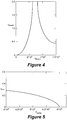
- the frequency response of the circuit with respect to the current is shown in Figure 4 .
- the purpose here is to run current through the filaments of the lamp, this is typically referred to as the 'Preheat' interval.
- the drive frequency is lowered. This causes the RLC circuit to be swept through its resonant frequency, causing an increase in the voltage across the lamp. An arc will occur in the lamp at its 'strike' voltage and the arc will ignite (ionize) the gas.
- Lamp 'ignition' means that the gas is now ionized enough to conduct an electric current.
- the lamp is now said to be on (producing visible light).
- Figure 3 best describes the behavior of the lamp ballast circuit.
- the lamp now behaves as an L in series with a parallel R and Cf.
- the R in this case is the electrical resistance of the ionized gas in the lamp and Cf is the filament capacitance 716.
- the frequency response of the circuit with respect to lamp current is shown in Figure 5 . Note that while the gas in the lamp is ionized, the current increases as the drive frequency is decreased. There is a point on the frequency response curve where the current is pinched off. Note that this point can be selectable by the ballast designer by manipulating the values of L and Cf.
- the lamp While the lamp is on, it will be driven at a frequency, F Low .
- the ballast designer may choose this drive frequency as optimal for the specified wattage of the fluorescent lamp. If the drive frequency is increased, that is the RLC circuit is de-tuned, the lamp will start to dim. As Figure 5 shows, the current though the gas in the lamp will decrease and so the light output will decrease with the decrease in current. As the drive frequency is increased, at some point between F Low and F High , the lamp will go out as the lamp current gets 'pinched' off.
- Dimming is accomplished by modulating the drive frequency to the RLC circuit.
- US Patent Application Publication US2002/0140371 discloses an integrated circuit for lamp heating and dimming control.
- US Patent Application Publication US2004/0263093 discloses an electrodeless light bulb type fluorescent lamp and discharge lamp lighting device.
- United States Patent US 5,440,324 discloses backlighting for a liquid crystal display.
- VCO voltage controlled oscillator
- a DC voltage is fed into the Modulator Input of the VCO and a square wave signal is generated.
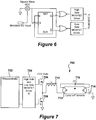
- the device identified as 'Logic Block' in Figures 1 through 3 converts the square wave into two drive signals on the gates of the power MOSFET transistors. A typical implementation of this circuit is shown in Figure 6 .
- the steepest slope on the curve is close to its 'pinch off point (around 60 kHz in Figure 5 ).
- small changes in frequency yield large changes in brightness.
- the method of dimming the lamp in this classic fluorescent lamp resonant circuit involves modulating the drive frequency. That is, as the frequency is raised linearly, the lamp brightness is lowered exponentially. This effect is not tolerant to coarse frequency modulation signals, especially at these low brightness levels. If the granularity of frequency control is too large, stepping from one frequency to another will result in a very visible brightness change; i.e., the lamp brightness is quantized.
- the following features are desired: (1) A way of varying the brightness of the lamp that compensates for thermal effects on the lamp. (2) Adequate resolution in the dimming circuit so brightness changes are smooth to the human eye and not visibly quantized. (3) 'Preheat' capability where the gas in the lamp is partially ionized and able to ignite without causing hot-spots to form on the filament. And (4) filament bias capability where the filaments are kept warm at low brightness levels to keep the lamp from going out and to prevent the filaments from developing 'hot spots.'
- digital electronic solutions offer the lighting industry precise and dependable control of their fluorescent lamp circuits.
- the operational performance of a digital component doesn't drift with temperature.
- the accuracy of digital logic is dependent upon the quality of its clock source, e.g., modern crystals and resonator devices are highly reliable, accurate and inexpensive. Since the performance of digital circuits don't change or worst case change insignificantly with age, their lifetime endurance may be higher.
- VCO voltage-controlled oscillator
- ASIC application specific integrated circuit
- PDA programmable logic array
- an inexpensive digital device e.g., a microcontroller
- a microcontroller in fluorescent lighting dimming control has many advantages. Since the functionality of the microcontroller may be dependent upon the software running in the microcontroller, lighting features may be implemented easily and inexpensively. The feature set required by a particular fluorescent dimming application may be custom tailored by the lamp manufacturer quickly and easily through custom software programming of the digital device, e.g., microcontroller.
- a method for controlling dimmable electronic lighting ballasts using pulse density modulation may comprise the steps of: generating a low frequency for a first time period, wherein the low frequency is approximately at a circuit resonant frequency of a dimmable electronic lighting ballast and a fluorescent lamp; and generating no frequency for a second time period; wherein the first and second time periods are within a modulation frame time period and the modulation frame time period that repeats continuously.
- a method for controlling dimmable electronic lighting ballasts using pulse density modulation may comprise the steps of: generating a low frequency for a first time period, wherein the low frequency is approximately at a circuit resonant frequency of a dimmable electronic lighting ballast and a fluorescent lamp; generating no frequency for a second time period; generating a high frequency for a third time period, wherein the high frequency is above the circuit resonant frequency of the dimmable electronic lighting ballast and the fluorescent lamp; wherein the first, second and third time periods are within a modulation frame time period and the modulation frame time period that repeats continuously.
- a dimmable fluorescent lamp system having an electronic lighting ballast using pulse density modulation for controlling the amount of light produced by the fluorescent lamp may comprise: a digital device having a first output and a second output; a first power switch having a control input coupled to the first output of the digital device; a second power switch having a control input coupled to the second output of the digital device; an inductor coupled to the first and second power switches, wherein the first power switch couples the inductor to a supply voltage, the second power switch couples the inductor to a supply voltage common, and the first and second power switches decouple the inductor from the supply voltage and supply voltage common, respectively; a direct current (DC) blocking capacitor coupled to the supply voltage common; a fluorescent lamp having first and second filaments, wherein the first filament is coupled to the inductor and the second filament is coupled to the DC blocking capacitor; and a filament capacitor coupling together the first and second filaments of the fluorescent lamp; wherein the digital device: generates a low frequency signal for
- a pulse density modulation technique for dimming a fluorescent lamp may be implemented by using an integrated circuit digital device, e.g., microcontroller integrated circuit.
- the pulse density modulation fluorescent lamp dimming circuit may comprise a microcontroller 702, a high and low side metal oxide semiconductor field effect transistor (MOSFET) driver 704, a high-side power MOSFET 706, a low-side power MOSFET 708, an inductor 710, a fluorescent lamp 712, a filament capacitor 716, and a DC blocking capacitor 714.
- MOSFET metal oxide semiconductor field effect transistor
- the MOSFET driver 704 may be used to translate the low output voltages of the microcontroller 702 to the high voltage levels required to operate the high side power MOSFET 706 and the low side power MOSFET 708.
- the microcontroller 702 may be used to switch the high-side driver ON or OFF, and the low-side drive OFF or On, respectively, of the MOSFET driver 704.
- the high-side power MOSFET 706 When the high-side drive is ON the high-side power MOSFET 706 allows current to flow through the resonant RLC fluorescent lamp circuit (inductor 710 and DC blocking capacitor 714) in one direction, and when the low-side drive is ON the low-side power MOSFET 708 allows current to flow through the resonant RLC fluorescent lamp circuit (inductor 710, fluorescent lamp 712 and DC blocking capacitor 714) in the other direction.
- the high-side power MOSFET 706 and the low-side power MOSFET 708 cannot be both ON at the same time. Also a dead band is desirable, e.g., the high-side power MOSFET 706 and the low-side power MOSFET 708 are both OFF. This may be easily accomplished with software instructions running in the microcontroller 702.
- the microcontroller 702 may synthesize an alternating current (AC) signal by alternatively turning on the high-side and low-side outputs of the MOSFET driver 704.
- AC alternating current
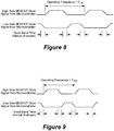
- FIGS 8 and 9 depicted are schematic waveform timing diagrams for low and high operating frequencies, F Low and F High respectively, according to a specific example embodiment of this disclosure.
- Figure 8 shows the low operating frequency waveform
- F Low shows the high operating frequency waveform.
- the high side drive signal is high
- the low side drive signal is low, and visa-versa.
- There is a dead band time where both the high side and the low side drive signals are low.
- These waveforms may be used to synthesize the following frequencies: F Low , F High and a DC signal (no current flow) when the high-side power MOSFET 706 and the low-side power MOSFET 708 are both off.
- the signals generated by the microcontroller 702 are effectively square waves with a duty cycle of, for example but not limited to, 50 percent.
- An alternative description of these AC signals is that of a pulse train. Within an interval of time, the actual number of these 'pulses' can be measured. A 'high' frequency signal will have more pulses in a given time interval than a 'low' frequency signal.
- An alternate method of measuring these signals is by their pulse density. At a fixed duty cycle, a high frequency signal has high pulse density; a low frequency signal has low pulse density.
- PDM Pulse Density Modulation
- the three synthesized frequencies referenced hereinabove may be defined as PDM states as follows: (1) State Off , (2) State Low , and (3) State High .
- PDM states For both of the active waveform states shown in Figures 8 and 9 , i.e., State Low and State High , respectively, there is a dead band interval between level transitions of the MOSFET drive signals from the microcontroller 702. This dead band interval assures that the currently active power MOSFET is given a sufficient amount of time to turn off before the complimentary power MOSFET is driven on.
- Dead-banding is a common technique that may be performed via the software running on the microcontroller 702.
- each cycle in State Low and State High is initiated by the assertion of the 'high-side' driver, followed by its de-assertion; then a dead band time interval, next the 'low-side' driver is asserted, and followed by its de-assertion.
- This cycle sequence repeats for the duration of these PDM states.
- Pulse Density Modulation may be used to achieve the aforementioned requirements (desired features) of a dimmable fluorescent lamp circuit. These requirements were stated previously and are repeated herein: (1) Vary the brightness of the fluorescent lamp so that thermal effects on the fluorescent lamp are compensated. (2) Obtain adequate resolution in the dimming circuit so brightness changes are smooth to the human eye and not visibly quantized. (3) 'Preheat' the filaments until the gas in the fluorescent lamp is partially ionized and able to ignite. And (4) maintain filament temperature at low brightness levels to keep the fluorescent lamp from going out and to prevent the filaments from developing 'hot spots.'
- the dimmer control system is initially in State Off .
- the dimmer control system is then subsequently brought into State High .
- the dimmer control system is best represented as the equivalent circuit shown in Figure 2 , and the filaments will have current passing through them, e.g., the fluorescent lamp is undergoing 'Preheating.'
- the dimmer control system may be kept in State High for a time deemed sufficient to warm the filaments to their 'Strike' temperature.
- the amount of time required for a particular dimmer control system to stay in State High will be a function of the physics of that particular fluorescent lamp, and is known to one skilled in fluorescent lamp technology.
- the lamp gas may now be ignited by having the dimmer control system enter the State Off .
- the filaments are now hot after the 'Preheat' interval.
- the last 'high-side' cycle of State High forced current into the inductor 710 of the RLC circuit.
- the assertion of the 'low-side' cycle only allows a path for current to flow.
- the inductor cannot allow current to instantaneously cease flowing so the voltage across the lamp will build until the gas 'strikes.'
- Figure 3 best represents the equivalent RLC circuit, at this point the fluorescent lamp is said to be 'lit.' Note that the time needed for this 'strike' to occur is very short, e.g., it is short enough to occur within the 'low-side' assertion interval.
- the dimmer control system When the lamp 712 is commanded to be at full brightness, the dimmer control system shall be constantly in State Low . In this PDM state, the dimmer control system is at a constant pulse density and it's equivalent circuit is best modeled as shown in Figure 3 . That is, when lit and running, and when commanded to be at full brightness, the power MOSFETs 706 and 708 are driven only at the State Low frequency.
- the dimmer control system is held in State Off , where the lamp RLC circuit is not driven at any frequency. Actually, it is not driven at all. Note that there are actually two states where there is substantially no lamp gas current, e.g., lamp gas is non-conducting. This no lamp gas current condition is when the lamp is being driven during State High and State Off . Only State Low causes current through the lamp gas.
- the system When commanded to be at some middle brightness, the system may be modulated between the State Low and State Off states. That is, when lit and running, the dimmer control system is brought from a full brightness state to a fully off state and back. The ratio between the State Off and State Low durations determines the apparent brightness of the lamp to the eye.
- Modulation of the pulse density needs to be at a rate faster than the human eye can notice.
- the human eye will notice flicker at a rate slower than about 30 Hz. If the modulation rate were much higher than this, flicker would not be an issue.
- modulating the pulse density of the lamp drive signals can control the apparent brightness of the lamp by toggling between the State Low and State Off states and controlling the amount of time spent in each of these states.
- Maintaining filament temperature so that no hot spots will develop may be accomplished by dividing the time that the lamp gas is not ionized, e.g., when in the State Off or State High states.
- Figure 10 depicted is a timing diagram of a 'Modulation Frame' that may be used to dim the lamp as well as maintain filament temperature, according to a specific example embodiment of this disclosure.
- Figure 10 shows the two MOSFET drive signals together for the purpose of clarity.
- the entire frame time is preferably less than one thirtieth of a second to avoid flicker, i.e., 1/30 is greater than or equal to t1 + t2 +t3 (Equation 1).
- time interval t1 is the duration of State Low
- time interval t2 is the duration of State Off
- time interval t3 is the duration of State High .
- the lamp is driven at full brightness as it is currently in State Low .
- the lamp is driven Off.
- Interval t2 has the lamp not driven at all.
- Interval t3 has the lamp circuit in State High .
- Figure 2 shows the appropriate equivalent circuit for the dimmer control system, and current is sent through the filaments, but the lamp gas is not ionized.
- the ABDC value, as with other Duty Cycle calculations may be expresses as a percentage.
- 100% ABDC means that the lamp is fully on (maximum brightness).
- a 0% ABDC means the lamp is fully Off (no light).
- the Maximum Lamp Power may be defined herein as the wattage when the lamp is run at 100% ABDC.
- the MLP is a function of the physics of the lamp and is well know to those having ordinary skill in the art of fluorescent lamps. What is important to know is that there is a specified maximum power value for the lamp(s) when it is driven at its low frequency value (F Low ).
- the Maximum Filament Power may be defined herein as the wattage when the lamp is run in State High continuously.
- the MFP is a function of the electrical resistance of the lamp filament and the choice of L and Cf, it is not important to this disclosure. Suffice it to say that there is a theoretical maximum power value for the lamp filament when it is driven at its high frequency value (F High ).
- a lamp filament will be able to maintain its minimum operating temperature through the use of software program steps running on the digital device. Thus, there is no need to incorporate any added circuitry to bias the filaments so as to maintain a certain desired temperature thereon.
- FIG. 11 depicted is a schematic diagram of the fluorescent lamp circuit of Figure 7 with a current sense resistor, according to another specific example embodiment of this disclosure.
- a sense resistor 1116 is added to the circuit of Figure 7 .
- feedback control of the apparent brightness may be implemented by measuring the current through the sense resistor 1116.
- the current through the sense resistor 1116 is substantially the same as the current through the lamp 712.
- the current through the sense resistor 1116 will produce a voltage across the sense resistor 1116 that is proportional to the lamp current.
- This voltage may be fed into an analog-to-digital converter (ADC) of the microcontroller 702a.
- ADC analog-to-digital converter
- the software running on the microcontroller 702a may now be used to determine a number of conditions of the operation of the fluorescent lamp 712. For example: (1) Has one of the filaments "burned out?" (2) What is the current through the filaments during preheat and is it excessive? (3) Is the lamp currently ON? And (4) what is
- the software program running in the microcontroller 702a may make decisions based upon the answers to these questions. If the lamp dimmer system is in State High , then conditions 1 and 2 may be determined. If no current is detected, then it is an open circuit, and so the filaments must be 'burned out.' The value that the ADC 1118 of the microcontroller 702a produces will tell the software program the present value of the lamp filament current. If the lamp dimmer system is in State Low , then conditions 3 and 4 may be determined. If no current is detected, then it is an open circuit, and so the lamp must be out. When lit, if the lamp current is outside where it is expected to be, then the ABDC can be adjusted to compensate.
- PID control Proportional, Integral, Differential
- a PID control loop may use this analog input representing lamp brightness to adjust the Apparent Brightness Duty Cycle (ABDC) so as to deliver a consistent perceived lamp brightness level.
- ABDC Apparent Brightness Duty Cycle
- the software program running on the microcontroller 702a may consider this as the demanded brightness level. A check of the current through the lamp will indicate the present apparent brightness of the lamp. If the values don't agree, the ABDC may be adjusted up or down to increase or decrease the Resultant Lamp Power (RLP), respectively. As the lamp increases or decreases in temperature because of its new brightness setting, the apparent brightness will drift. The feedback control via the microcontroller's software program will maintain the demanded brightness regardless of temperature transitions (e.g., drift or transients) in the lamp 712.
- temperature transitions e.g., drift or transients
- the Pulse Density Modulation (PDM) technique disclosed herein allows for easy implementation of a software feedback control program in the microcontroller 702a, according teachings of this disclosure. While maintaining the user desired brightness of the fluorescent lamp 712, this PDM technique may maintain temperature on the lamp filaments, thus extending the life the lamp filaments and also preventing the fluorescent lamp 712 from going out due to low filament temperature.
- PDM Pulse Density Modulation
- the MOSFET drivers 704 may be driven directly from General Purpose I/O pins of the microcontroller 702. This eliminates the need for costly VCO circuits on or with the microcontroller.
- deadbanding may be implemented with a software program running in the microcontroller 702, thus eliminating the need for external logic circuits to perform this task.
- the lamp may be started via pre-heating the filaments and striking the gas ionization under control of the software program running in the microcontroller 702.
- the software program may dim the fluorescent lamp 712 via the PDM, and the number of brightness levels may be so numerous (very fine granularity) that 'sweeping' through them would appear as smooth as that seen with dimming of incandescent lamps.
- a low pin count microcontroller may be used to implement the lamp dimmer system, resulting in quite a cost savings for the manufacturer as well as a wealth of reliability and functionality improvement to their products.
- the digital device may be used, with appropriate software programming to: (1) active power factor correction (PFC) to increase lamp efficiency, (2) remote control protocols such as digital addressable lighting interface (DALI), IEEE 802.15.04 or Zigbee, and/or (3) battery charging for emergency lighting ballasts.
- the software program may be stored in nonvolatile memory and may be implemented in the digital device as "firmware.”
- a relatively inexpensive digital device, e.g., microcontroller, may run from an internal clock oscillator.
- FIG. 12 depicted is a schematic block diagram of a predominately hardware implementation of a PDM generation peripheral for a lamp dimmer system, according to still another specific example embodiment of this disclosure.
- the predominately hardware implementation may be accomplished with a digital device, e.g., microcontroller, generally represented by the numeral 1200.
- the microcontroller may be used as a hardware peripheral that would automatically create the required control signals necessary to control operation and dimming of a fluorescent lamp(s) and require only minimum software program overhead.
- the pulse density modulation (PDM) scheme is relatively simple in concept and may easily be implemented in firmware in the microcontroller 1200.
- PFC active power factor correction
- the microcontroller 1200 may be configured for and comprise the following functional blocks.
- a Frame Sequencer Block 1202 a Frame Sequencer Timebase 1204, a Frequency Generator Block 1206, a Frequency Generator Timebase 1208, and a Dead-Time Generator 1210.
- the Dead-Time Generator 1210 may have FGH 1212 and FGL 1214 outputs and a /FAULT 1216 input.
- the Frame Sequencer Timebase 1204 and Frequency Generator Timebase 1208 may be basic synchronous timers having a system clock input, a prescaler and a timebase.
- the Frame Sequencer Block 1202 may be used to specify the duration of each phase within a lamp driving frame, as shown in Figure 13 .
- the duration of the frame may be specified by the rollover period of the Frame Sequencer Timebase 1208.
- There are two compare registers which specify the end of the pre-heat (State High . - high-frequency - F High ) and the lamp-on (State Low - resonant frequency - F Low ) periods.
- the lamp may be off (State Off ) for the remainder of the Frame Sequencer period.
- the Frequency Generator Block 1206 may have two period registers so that two different frequencies may be generated.
- the Frame Sequencer Block 1202 sends control signals to the Frequency Generator Block 1206 that specify which period (frequency) to use.
- the first preheat frequency may be skipped if the Pre-heat Compare time is 0.
- the output will always be 0 (off) during the third phase of the frame.
- the Frequency Generator block 1206 will wait for the end of a period before switching to the next frequency state.
- the Dead Time Generator 1210 may generate complementary output signals, FGH 1212 and FGL 1214, having switching delay between each transition.
- the Dead Time Generator 1210 may be used to drive a half-bridge inverter circuit, e.g., power MOSFETs 706 and 708.
- An asynchronous shutdown input /FAULT 1216 may also be provided for external hardware faults.
- FIG. 14 depicted is a schematic block diagram of a software assisted PDM generation peripheral for a lamp dimmer system, according to yet another specific example embodiment of this disclosure.
- the amount of hardware required to implement a PDM generation peripheral may be cost prohibitive. If this is the case, a 'software assisted' version of the PDM generation peripheral may be implemented as shown in Figure 14 .
- the PDM generation peripheral may be easily and inexpensively implemented using currently available microcontroller hardware.
- An Enhanced Capture/Compare/PWM (ECCP) module with timebase 1402 and output logic 1404 may be used to generate the frequency output to the lamp ballast inverter, e.g., power MOSFETs 706 and 708.
- the ECCP timebase interrupt signal 1406 may be routed internally to a second timebase 1408 and used to increment that timebase 1408.
- the second timebase 1408 keeps track of the time spent in each frequency state (see Figure 13 ). Therefore, the central processing unit (CPU) of the microprocessor is only interrupted when the second timebase 1408 overflows (interrupt 1410).
- CPU central processing unit
- This process is analogous to a microcontroller motor control where the CPU only needs to be interrupted at commutation events, which occur at a much lower rate than does the PWM frequency.
- a new period register 1412 and duty cycle register 1414 may be loaded at each interrupt event of the second timebase 1408.
- the output logic 1404 may have the ability to be placed in the 'OFF' state and still keep the ECCP timebase 1402 running. This allows for timing of the 'OFF' state (State Off ) by software control from the microcontroller.
Landscapes
- Discharge-Lamp Control Circuits And Pulse- Feed Circuits (AREA)
- Circuit Arrangements For Discharge Lamps (AREA)
Claims (15)
- Verfahren zur Steuerung eines verdunkelbaren Vorschaltgeräts (704,706,708) für eine Fluoreszenzlampe (712) unter Verwendung von Modulation von Impulsdichte, wobei die Fluoreszenzlampe (712) erste und zweite Glühfäden aufweist, wobei ein Glühfadenkondensator (716) die ersten und zweiten Glühfäden der Fluoreszenzlampe (712) miteinander koppelt und wobei der erste Glühfaden mit einer Drossel (710) gekoppelt ist und der zweite Glühfaden mit einem Gleichstromabblockkondensator (714) gekoppelt ist, wodurch eine in Reihe verbundene Schaltung ausgebildet wird, wobei das Verfahren die nachfolgenden Schritte aufweist:Erzeugen eines Hochfrequenzsteuersignals, das für eine erste Zeitdauer durch die Drossel (710) in das Vorschaltgerät (716) gespeist wird, wobei die Hochfrequenz oberhalb einer Resonanzfrequenz der in Reihe verbundenen Schaltung liegt;Erzeugen eines Niederfrequenzsteuersignals, das für eine zweite Zeitdauer durch die Drossel (710) in das Vorschaltgerät eingespeist wird, wobei die Niederfrequenz in etwa bei einer Resonanzfrequenz der in Reihe verbundenen Schaltung liegt; undErzeugen keiner Frequenz für eine dritte Zeitdauer;wobei die ersten, zweiten und dritten Zeitdauern innerhalb einer Modulationsabschnittszeitdauer liegen und sich die Modulationsabschnittszeitdauer fortlaufend wiederholt.
- Verdunkelbares Fluoreszenzlampensystem mit einer Fluoreszenzlampe (712), die erste und zweite Glühfäden aufweist, wobei ein Glühfadenkondensator (716) die ersten und zweiten Glühfäden der Fluoreszenzlampe (712) miteinander koppelt und wobei der erste Glühfaden mit einer Drossel (710) gekoppelt ist und der zweite Glühfaden mit einem Gleichstromabblockkondensator (714) gekoppelt ist, wodurch eine in Reihe verbundene Schaltung ausgebildet wird, wobei die System programmierbare Mittel zur Erzeugung von Impulsen (702, 702a; 704) aufweist, im Besonderen einen Mikrocontroller (702, 702a) aufweist,
dadurch gekennzeichnet, dass
die Mittel zur Erzeugung von Impulsen (702, 702a; 704) Verfahrensschritte gemäß Anspruch 1 ausführen. - Verdunkelbares Fluoreszenzlampensystem gemäß Anspruch 2, wobei die Mittel zur Impulserzeugung eine digitale Anordnung (702; 702a) aufweisen, die einen ersten Ausgang und einen zweiten Ausgang aufweist, und das System weiterhin aufweist:einen ersten Netzschalter (706), der einen mit dem ersten Ausgang der digitalen Anordnung (702; 702a) gekoppelten Steuereingang aufweist;einen zweiten Netzschalter (708), der einen mit dem zweiten Ausgang der digitalen Anordnung (702; 702a) gekoppelten Steuereingang aufweist;wobei die Drossel (710) mit den ersten und zweiten Netzschaltern (706, 708) gekoppelt ist, wobei der erste Netzschalter (706) die Drossel (710) mit einer Versorgungsspannung koppelt, der zweite Netzschalter (708) die Drossel (710) mit einer gemeinsamen Versorgungsspannungsleitung koppelt, und die ersten und zweiten Netzschalter (706, 708) die Drossel (710) von der Versorgungsspannung beziehungsweise der gemeinsamen Versorgungsspannungsleitung entkoppeln; undwobei der Gleichstrom- (DC) Abblockkondensator (714) mit der gemeinsamen Versorgungsspannungsleitung gekoppelt ist.
- Verfahren oder System gemäß einem der vorherigen Ansprüche, wobei die zweite Zeitdauer im Wesentlichen 100 Prozent der Modulationsabschnittszeitdauer ist, wenn die Fluoreszenzlampe maximale Helligkeit aufweist und/oder wobei die dritte Zeitdauer im Wesentlichen 100 Prozent der Modulationsabschnittszeitdauer ist, wenn die Fluoreszenzlampe ausgeschaltet ist und/oder wobei die zweite Zeitdauer geringer als 100 Prozent der Modulationsabschnittszeitdauer ist, wenn die Fluoreszenzlampe weniger als die maximale Helligkeit aufweist.
- Verfahren oder System gemäß einem der vorherigen Ansprüche, wobei die Modulationsabschnittszeitdauer geringer oder gleich 1/30 einer Sekunde ist.
- Verfahren oder System gemäß einem der vorherigen Ansprüche, wobei die erste Zeitdauer ausreichend Prozent der Modulationsabschnittszeitdauer beträgt, um die Glühfäden der Fluoreszenzlampe warm zu halten.
- Verfahren oder System gemäß Anspruch 4, wobei ein Fluoreszenzlampenstrom durch einen Fluoreszenzlampenstrommesswiderstand gemessen wird, der zwischen dem Gleichstromabblockkondensator (714) und der gemeinsamen Versorgungsspannungsleitung gekoppelt ist.
- Verfahren gemäß Anspruch 7, das weiterhin den Schritt des Bestimmens von Zuständen der Fluoreszenzlampe (712) aus dem gemessenen Fluoreszenzlampenstrom aufweist, wobei die Zustände der Fluoreszenzlampe (712) ausgewählt werden aus der Gruppe bestehend aus Glühfadenausbrennen, übermäßigem Glühfadenstrom während des Vorheizens, Fluoreszenzlampe eingeschaltet und Strom durch die erleuchtete Fluoreszenzlampe.
- Verfahren oder System gemäß Anspruch 7, wobei der zweite Zeitdauerprozentsatz der Modulationsabschnittszeitdauer derart eingestellt wird, dass der gemessene Fluoreszenzlampenstrom auf einem erwünschten Wert gehalten wird.
- Verfahren oder System gemäß Anspruch 7, wobei die Prozentsätze der Modulationsabschnittszeitdauer der dritten Zeitdauer und der ersten Zeitdauer derart eingestellt werden, dass die Glühfäden der Fluoreszenzlampe auf einer erwünschten Temperatur gehalten werden.
- Verfahren gemäß einem der vorherigen Ansprüche 1, 4 bis 10, das weiterhin den Schritt des Korrigierens eines Wirkfaktors aufweist.
- Verfahren gemäß einem der vorherigen Ansprüche 1, 4 bis 11, das weiterhin den Schritt des Fernsteuerns der zweiten und dritten Zeitdauern aufweist, um die Lichtleistung der Fluoreszenzlampe fernzusteuern, vorzugsweise mit einem Digital Addressable Lighting Interface (DALI) Protokoll, mit einem Zigbee-Protokoll, oder mit einem IEEE 802.15.4-Protokoll.
- Verfahren gemäß einem der vorherigen Ansprüche, das weiterhin den Schritt des Steuerns eines Batterieladegeräts für Notfallbeleuchtung aufweist.
- System gemäß Anspruch 3, wobei die digitale Anordnung (702; 702a) aufweist:einen Frame-Sequenzerblock (1202);einen Frame-Sequenzertaktgeber (1204);einen Frequenzgeneratorblock (1206);einen Frequenzgeneratortaktgeber (1208); undeinen Ausschaltzeitgenerator (1210);wobeider Frame-Sequenzerblock (1202) die ersten, zweiten und dritten Zeitdauern festlegt,der Frequenzgeneratorblock (1206) die Hoch- und Niederfrequenzsignale festlegt, undder Ausschaltzeitgenerator (1210) verhindert, dass die ersten und zweiten Netzschalter beide zur gleichen Zeit eingeschaltet sind.
- System gemäß einem der vorherigen Ansprüche 3 bis 7 oder 14, wobei die digitale Anordnung (702; 702a) mit einem Softwareprogramm gesteuert wird.
Applications Claiming Priority (2)
| Application Number | Priority Date | Filing Date | Title |
|---|---|---|---|
| US11/470,052 US7642735B2 (en) | 2006-09-05 | 2006-09-05 | Using pulse density modulation for controlling dimmable electronic lighting ballasts |
| PCT/US2007/077200 WO2008030751A2 (en) | 2006-09-05 | 2007-08-30 | Using pulse density modulation for controlling dimmable electronic lighting ballasts |
Publications (2)
| Publication Number | Publication Date |
|---|---|
| EP2080422A2 EP2080422A2 (de) | 2009-07-22 |
| EP2080422B1 true EP2080422B1 (de) | 2018-06-27 |
Family
ID=38917782
Family Applications (1)
| Application Number | Title | Priority Date | Filing Date |
|---|---|---|---|
| EP07841596.5A Active EP2080422B1 (de) | 2006-09-05 | 2007-08-30 | Modulation von impulsdichte zur steuerung von verdunkelbaren elektronischen beleuchungsvorschaltgeräten |
Country Status (5)
| Country | Link |
|---|---|
| US (1) | US7642735B2 (de) |
| EP (1) | EP2080422B1 (de) |
| KR (1) | KR101133083B1 (de) |
| CN (1) | CN101518160B (de) |
| WO (1) | WO2008030751A2 (de) |
Families Citing this family (18)
| Publication number | Priority date | Publication date | Assignee | Title |
|---|---|---|---|---|
| US8729828B2 (en) * | 2007-06-15 | 2014-05-20 | System General Corp. | Integrated circuit controller for ballast |
| US8044899B2 (en) * | 2007-06-27 | 2011-10-25 | Hong Kong Applied Science and Technology Research Institute Company Limited | Methods and apparatus for backlight calibration |
| US7952303B2 (en) | 2008-03-13 | 2011-05-31 | Universal Lighting Technologies, Inc. | Electronic ballast for a gas discharge lamp with controlled filament heating during dimming |
| EP2124510B1 (de) * | 2008-05-16 | 2013-01-02 | Infineon Technologies Austria AG | Verfahren zur Ansteuerung einer Leuchtstofflampe und Lampenvorschaltgerät |
| US8373357B2 (en) | 2009-01-26 | 2013-02-12 | Microchip Technology Incorporated | Modulator module in an integrated circuit device |
| US8698414B2 (en) * | 2009-04-13 | 2014-04-15 | Microchip Technology Incorporated | High resolution pulse width modulation (PWM) frequency control using a tunable oscillator |
| US20100329941A1 (en) * | 2009-06-30 | 2010-12-30 | Mark Edward Moore | Output control for ozone generators |
| US8536801B1 (en) | 2009-11-11 | 2013-09-17 | Universal Lighting Technologies, Inc. | System and method for individually modulating an array of light emitting devices |
| EP2418512A1 (de) * | 2010-07-30 | 2012-02-15 | Mechaless Systems GmbH | Optoelektronische Messanordnung mit Fremdlichtkompensation |
| US8816604B2 (en) | 2012-08-03 | 2014-08-26 | Ge Lighting Solutions, Llc. | Dimming control method and apparatus for LED light source |
| US9041312B2 (en) | 2012-08-28 | 2015-05-26 | Abl Ip Holding Llc | Lighting control device |
| US9547319B2 (en) | 2012-08-28 | 2017-01-17 | Abl Ip Holding Llc | Lighting control device |
| US9794999B2 (en) * | 2013-04-04 | 2017-10-17 | Ledengin, Inc. | Color tunable light source module with brightness and dimming control |
| US9270180B2 (en) * | 2013-05-03 | 2016-02-23 | Texas Instruments Deutschland Gmbh | DC-DC converter with adaptive minimum on-time |
| US9307623B1 (en) * | 2013-07-18 | 2016-04-05 | Universal Lighting Technologies, Inc. | Method to control striations in a lamp powered by an electronic ballast |
| US9468069B2 (en) | 2014-04-03 | 2016-10-11 | Ledengin, Inc. | Smooth brightness adjustment for color-tunable light source module |
| CN104540312B (zh) * | 2015-01-08 | 2017-01-11 | 福州大学 | 一种适用于电磁感应灯的调光方法 |
| US9966959B2 (en) | 2016-07-19 | 2018-05-08 | Altera Corporation | Feedback control systems with pulse density signal processing capabilities |
Family Cites Families (13)
| Publication number | Priority date | Publication date | Assignee | Title |
|---|---|---|---|---|
| US5440324A (en) * | 1992-12-30 | 1995-08-08 | Avionic Displays Corporation | Backlighting for liquid crystal display |
| CH690486A5 (it) * | 1995-07-11 | 2000-09-15 | Bob Hammer Systems Solutions S | Dispositivo per la gestione di lampade fluorescenti. |
| US6002213A (en) * | 1995-10-05 | 1999-12-14 | International Rectifier Corporation | MOS gate driver circuit with analog input and variable dead time band |
| US6094016A (en) * | 1997-03-04 | 2000-07-25 | Tridonic Bauelemente Gmbh | Electronic ballast |
| DE60122727T2 (de) * | 2000-05-12 | 2007-09-13 | 02 Micro International Ltd. | Intregrierte schaltung zur lampenerwärmung und dimmersteuerung |
| EP1401091A4 (de) | 2001-06-27 | 2005-09-28 | Matsushita Electric Industrial Co Ltd | Kalt-kathoden-treiber und flüssigkristallanzeige |
| US6583568B1 (en) * | 2001-12-19 | 2003-06-24 | Northrop Grumman | Method and apparatus for dimming high-intensity fluorescent lamps |
| US7009348B2 (en) * | 2002-06-03 | 2006-03-07 | Systel Development & Industries Ltd. | Multiple channel ballast and networkable topology and system including power line carrier applications |
| US6977472B2 (en) * | 2002-06-07 | 2005-12-20 | Matsushita Electric Industrial Co., Ltd. | Electrodeless self-ballasted fluorescent lamp and discharge lamp operating device |
| US6956336B2 (en) * | 2002-07-22 | 2005-10-18 | International Rectifier Corporation | Single chip ballast control with power factor correction |
| JP4156324B2 (ja) * | 2002-09-30 | 2008-09-24 | ローム株式会社 | 直流−交流変換装置、及び交流電力供給方法 |
| TWI232070B (en) * | 2003-02-27 | 2005-05-01 | Chi Mei Optoelectronics Corp | Device and method to dynamically adjust the burst mode switching frequency for LCD |
| US7183692B2 (en) * | 2004-12-13 | 2007-02-27 | Zippy Technology Corp. | Method for controlling power supply in a buffered modulation mode |
-
2006
- 2006-09-05 US US11/470,052 patent/US7642735B2/en active Active
-
2007
- 2007-08-30 EP EP07841596.5A patent/EP2080422B1/de active Active
- 2007-08-30 KR KR1020097006607A patent/KR101133083B1/ko active Active
- 2007-08-30 WO PCT/US2007/077200 patent/WO2008030751A2/en not_active Ceased
- 2007-08-30 CN CN200780034325XA patent/CN101518160B/zh active Active
Non-Patent Citations (1)
| Title |
|---|
| None * |
Also Published As
| Publication number | Publication date |
|---|---|
| KR20090051243A (ko) | 2009-05-21 |
| US7642735B2 (en) | 2010-01-05 |
| WO2008030751A3 (en) | 2008-05-08 |
| EP2080422A2 (de) | 2009-07-22 |
| CN101518160A (zh) | 2009-08-26 |
| CN101518160B (zh) | 2013-11-20 |
| KR101133083B1 (ko) | 2012-04-04 |
| WO2008030751A2 (en) | 2008-03-13 |
| US20080054825A1 (en) | 2008-03-06 |
Similar Documents
| Publication | Publication Date | Title |
|---|---|---|
| EP2080422B1 (de) | Modulation von impulsdichte zur steuerung von verdunkelbaren elektronischen beleuchungsvorschaltgeräten | |
| EP2420111B1 (de) | Hochauflösende impulsbreitenmodulations-(pwm-) frequenzregelung unter verwendung eines abstimmbaren oszillators | |
| US5424611A (en) | Method for pre-heating a gas-discharge lamp | |
| CN1251558C (zh) | 用于灯具加热和减光控制的集成电路 | |
| JP3752222B2 (ja) | 高輝度放電ランプ用の調光可能な電子安定器 | |
| US20020097008A1 (en) | Microcontroller, switched-mode power supply, ballast for operating at least one electric lamp, and method of operating at least one electric lamp | |
| TW200529704A (en) | Full digital dimming ballast for a fluorescent lamp | |
| JPH10337035A (ja) | 圧電トランスの駆動回路 | |
| JP2004208396A (ja) | 直流−交流変換装置、及びそのコントローラic | |
| JP2005019375A (ja) | 非同期pwm駆動方式のlcdパネル用バックライトインバータ | |
| US8193719B2 (en) | Using pulse density modulation for controlling dimmable electronic lighting ballasts | |
| JPS63148598A (ja) | 高圧ガス放電灯作動用回路 | |
| US8063588B1 (en) | Single-input control circuit for programming electronic ballast parameters | |
| KR20100114100A (ko) | 적어도 하나의 광원을 구동하기 위한 전자 안정기 및 방법 | |
| JP2007005285A (ja) | 冷陰極蛍光ランプの駆動装置 | |
| JP4679153B2 (ja) | 高輝度放電灯の2つの状態の動作 | |
| US20060279235A1 (en) | Driving apparatus for ccfl | |
| CN101584253A (zh) | 放电灯点灯装置,照明装置和液晶显示装置 | |
| JP3315744B2 (ja) | 調光用放電灯点灯装置 | |
| JP2008504647A (ja) | 蛍光管ランプ駆動回路 | |
| JP2006520129A (ja) | デジタル照明安定器発振器 | |
| JP2010511969A (ja) | 放電ランプの電極加熱のための方法及び回路 | |
| JP3516210B2 (ja) | プッシュプルインバ−タ | |
| JP2010040209A (ja) | 液晶パネル用バックライト装置 | |
| JPH1126180A (ja) | 放電灯点灯装置 |
Legal Events
| Date | Code | Title | Description |
|---|---|---|---|
| PUAI | Public reference made under article 153(3) epc to a published international application that has entered the european phase |
Free format text: ORIGINAL CODE: 0009012 |
|
| 17P | Request for examination filed |
Effective date: 20090403 |
|
| AK | Designated contracting states |
Kind code of ref document: A2 Designated state(s): AT BE BG CH CY CZ DE DK EE ES FI FR GB GR HU IE IS IT LI LT LU LV MC MT NL PL PT RO SE SI SK TR |
|
| DAX | Request for extension of the european patent (deleted) | ||
| 17Q | First examination report despatched |
Effective date: 20110512 |
|
| R17D | Deferred search report published (corrected) |
Effective date: 20080508 |
|
| STAA | Information on the status of an ep patent application or granted ep patent |
Free format text: STATUS: EXAMINATION IS IN PROGRESS |
|
| GRAP | Despatch of communication of intention to grant a patent |
Free format text: ORIGINAL CODE: EPIDOSNIGR1 |
|
| STAA | Information on the status of an ep patent application or granted ep patent |
Free format text: STATUS: GRANT OF PATENT IS INTENDED |
|
| INTG | Intention to grant announced |
Effective date: 20180130 |
|
| GRAS | Grant fee paid |
Free format text: ORIGINAL CODE: EPIDOSNIGR3 |
|
| GRAA | (expected) grant |
Free format text: ORIGINAL CODE: 0009210 |
|
| STAA | Information on the status of an ep patent application or granted ep patent |
Free format text: STATUS: THE PATENT HAS BEEN GRANTED |
|
| AK | Designated contracting states |
Kind code of ref document: B1 Designated state(s): AT BE BG CH CY CZ DE DK EE ES FI FR GB GR HU IE IS IT LI LT LU LV MC MT NL PL PT RO SE SI SK TR |
|
| REG | Reference to a national code |
Ref country code: GB Ref legal event code: FG4D |
|
| REG | Reference to a national code |
Ref country code: AT Ref legal event code: REF Ref document number: 1013475 Country of ref document: AT Kind code of ref document: T Effective date: 20180715 |
|
| REG | Reference to a national code |
Ref country code: IE Ref legal event code: FG4D |
|
| REG | Reference to a national code |
Ref country code: DE Ref legal event code: R096 Ref document number: 602007055231 Country of ref document: DE |
|
| REG | Reference to a national code |
Ref country code: FR Ref legal event code: PLFP Year of fee payment: 12 |
|
| PG25 | Lapsed in a contracting state [announced via postgrant information from national office to epo] |
Ref country code: SE Free format text: LAPSE BECAUSE OF FAILURE TO SUBMIT A TRANSLATION OF THE DESCRIPTION OR TO PAY THE FEE WITHIN THE PRESCRIBED TIME-LIMIT Effective date: 20180627 Ref country code: FI Free format text: LAPSE BECAUSE OF FAILURE TO SUBMIT A TRANSLATION OF THE DESCRIPTION OR TO PAY THE FEE WITHIN THE PRESCRIBED TIME-LIMIT Effective date: 20180627 Ref country code: BG Free format text: LAPSE BECAUSE OF FAILURE TO SUBMIT A TRANSLATION OF THE DESCRIPTION OR TO PAY THE FEE WITHIN THE PRESCRIBED TIME-LIMIT Effective date: 20180927 Ref country code: LT Free format text: LAPSE BECAUSE OF FAILURE TO SUBMIT A TRANSLATION OF THE DESCRIPTION OR TO PAY THE FEE WITHIN THE PRESCRIBED TIME-LIMIT Effective date: 20180627 |
|
| REG | Reference to a national code |
Ref country code: NL Ref legal event code: MP Effective date: 20180627 |
|
| REG | Reference to a national code |
Ref country code: LT Ref legal event code: MG4D |
|
| PG25 | Lapsed in a contracting state [announced via postgrant information from national office to epo] |
Ref country code: GR Free format text: LAPSE BECAUSE OF FAILURE TO SUBMIT A TRANSLATION OF THE DESCRIPTION OR TO PAY THE FEE WITHIN THE PRESCRIBED TIME-LIMIT Effective date: 20180928 Ref country code: LV Free format text: LAPSE BECAUSE OF FAILURE TO SUBMIT A TRANSLATION OF THE DESCRIPTION OR TO PAY THE FEE WITHIN THE PRESCRIBED TIME-LIMIT Effective date: 20180627 |
|
| REG | Reference to a national code |
Ref country code: AT Ref legal event code: MK05 Ref document number: 1013475 Country of ref document: AT Kind code of ref document: T Effective date: 20180627 |
|
| PG25 | Lapsed in a contracting state [announced via postgrant information from national office to epo] |
Ref country code: NL Free format text: LAPSE BECAUSE OF FAILURE TO SUBMIT A TRANSLATION OF THE DESCRIPTION OR TO PAY THE FEE WITHIN THE PRESCRIBED TIME-LIMIT Effective date: 20180627 |
|
| PG25 | Lapsed in a contracting state [announced via postgrant information from national office to epo] |
Ref country code: RO Free format text: LAPSE BECAUSE OF FAILURE TO SUBMIT A TRANSLATION OF THE DESCRIPTION OR TO PAY THE FEE WITHIN THE PRESCRIBED TIME-LIMIT Effective date: 20180627 Ref country code: CZ Free format text: LAPSE BECAUSE OF FAILURE TO SUBMIT A TRANSLATION OF THE DESCRIPTION OR TO PAY THE FEE WITHIN THE PRESCRIBED TIME-LIMIT Effective date: 20180627 Ref country code: EE Free format text: LAPSE BECAUSE OF FAILURE TO SUBMIT A TRANSLATION OF THE DESCRIPTION OR TO PAY THE FEE WITHIN THE PRESCRIBED TIME-LIMIT Effective date: 20180627 Ref country code: AT Free format text: LAPSE BECAUSE OF FAILURE TO SUBMIT A TRANSLATION OF THE DESCRIPTION OR TO PAY THE FEE WITHIN THE PRESCRIBED TIME-LIMIT Effective date: 20180627 Ref country code: IS Free format text: LAPSE BECAUSE OF FAILURE TO SUBMIT A TRANSLATION OF THE DESCRIPTION OR TO PAY THE FEE WITHIN THE PRESCRIBED TIME-LIMIT Effective date: 20181027 Ref country code: PL Free format text: LAPSE BECAUSE OF FAILURE TO SUBMIT A TRANSLATION OF THE DESCRIPTION OR TO PAY THE FEE WITHIN THE PRESCRIBED TIME-LIMIT Effective date: 20180627 Ref country code: SK Free format text: LAPSE BECAUSE OF FAILURE TO SUBMIT A TRANSLATION OF THE DESCRIPTION OR TO PAY THE FEE WITHIN THE PRESCRIBED TIME-LIMIT Effective date: 20180627 |
|
| PG25 | Lapsed in a contracting state [announced via postgrant information from national office to epo] |
Ref country code: IT Free format text: LAPSE BECAUSE OF FAILURE TO SUBMIT A TRANSLATION OF THE DESCRIPTION OR TO PAY THE FEE WITHIN THE PRESCRIBED TIME-LIMIT Effective date: 20180627 Ref country code: ES Free format text: LAPSE BECAUSE OF FAILURE TO SUBMIT A TRANSLATION OF THE DESCRIPTION OR TO PAY THE FEE WITHIN THE PRESCRIBED TIME-LIMIT Effective date: 20180627 |
|
| REG | Reference to a national code |
Ref country code: DE Ref legal event code: R097 Ref document number: 602007055231 Country of ref document: DE |
|
| PG25 | Lapsed in a contracting state [announced via postgrant information from national office to epo] |
Ref country code: MC Free format text: LAPSE BECAUSE OF FAILURE TO SUBMIT A TRANSLATION OF THE DESCRIPTION OR TO PAY THE FEE WITHIN THE PRESCRIBED TIME-LIMIT Effective date: 20180627 |
|
| REG | Reference to a national code |
Ref country code: CH Ref legal event code: PL |
|
| PG25 | Lapsed in a contracting state [announced via postgrant information from national office to epo] |
Ref country code: LU Free format text: LAPSE BECAUSE OF NON-PAYMENT OF DUE FEES Effective date: 20180830 Ref country code: CH Free format text: LAPSE BECAUSE OF NON-PAYMENT OF DUE FEES Effective date: 20180831 Ref country code: LI Free format text: LAPSE BECAUSE OF NON-PAYMENT OF DUE FEES Effective date: 20180831 |
|
| PLBE | No opposition filed within time limit |
Free format text: ORIGINAL CODE: 0009261 |
|
| STAA | Information on the status of an ep patent application or granted ep patent |
Free format text: STATUS: NO OPPOSITION FILED WITHIN TIME LIMIT |
|
| REG | Reference to a national code |
Ref country code: BE Ref legal event code: MM Effective date: 20180831 |
|
| GBPC | Gb: european patent ceased through non-payment of renewal fee |
Effective date: 20180927 |
|
| PG25 | Lapsed in a contracting state [announced via postgrant information from national office to epo] |
Ref country code: DK Free format text: LAPSE BECAUSE OF FAILURE TO SUBMIT A TRANSLATION OF THE DESCRIPTION OR TO PAY THE FEE WITHIN THE PRESCRIBED TIME-LIMIT Effective date: 20180627 |
|
| 26N | No opposition filed |
Effective date: 20190328 |
|
| PG25 | Lapsed in a contracting state [announced via postgrant information from national office to epo] |
Ref country code: SI Free format text: LAPSE BECAUSE OF FAILURE TO SUBMIT A TRANSLATION OF THE DESCRIPTION OR TO PAY THE FEE WITHIN THE PRESCRIBED TIME-LIMIT Effective date: 20180627 Ref country code: BE Free format text: LAPSE BECAUSE OF NON-PAYMENT OF DUE FEES Effective date: 20180831 |
|
| PG25 | Lapsed in a contracting state [announced via postgrant information from national office to epo] |
Ref country code: GB Free format text: LAPSE BECAUSE OF NON-PAYMENT OF DUE FEES Effective date: 20180927 |
|
| PG25 | Lapsed in a contracting state [announced via postgrant information from national office to epo] |
Ref country code: MT Free format text: LAPSE BECAUSE OF NON-PAYMENT OF DUE FEES Effective date: 20180830 |
|
| PG25 | Lapsed in a contracting state [announced via postgrant information from national office to epo] |
Ref country code: TR Free format text: LAPSE BECAUSE OF FAILURE TO SUBMIT A TRANSLATION OF THE DESCRIPTION OR TO PAY THE FEE WITHIN THE PRESCRIBED TIME-LIMIT Effective date: 20180627 |
|
| PG25 | Lapsed in a contracting state [announced via postgrant information from national office to epo] |
Ref country code: PT Free format text: LAPSE BECAUSE OF FAILURE TO SUBMIT A TRANSLATION OF THE DESCRIPTION OR TO PAY THE FEE WITHIN THE PRESCRIBED TIME-LIMIT Effective date: 20180627 Ref country code: HU Free format text: LAPSE BECAUSE OF FAILURE TO SUBMIT A TRANSLATION OF THE DESCRIPTION OR TO PAY THE FEE WITHIN THE PRESCRIBED TIME-LIMIT; INVALID AB INITIO Effective date: 20070830 |
|
| PG25 | Lapsed in a contracting state [announced via postgrant information from national office to epo] |
Ref country code: IE Free format text: LAPSE BECAUSE OF NON-PAYMENT OF DUE FEES Effective date: 20180830 Ref country code: CY Free format text: LAPSE BECAUSE OF FAILURE TO SUBMIT A TRANSLATION OF THE DESCRIPTION OR TO PAY THE FEE WITHIN THE PRESCRIBED TIME-LIMIT Effective date: 20180627 |
|
| P01 | Opt-out of the competence of the unified patent court (upc) registered |
Effective date: 20230528 |
|
| PGFP | Annual fee paid to national office [announced via postgrant information from national office to epo] |
Ref country code: DE Payment date: 20250724 Year of fee payment: 19 |
|
| PGFP | Annual fee paid to national office [announced via postgrant information from national office to epo] |
Ref country code: FR Payment date: 20250725 Year of fee payment: 19 |