EP2420111B1 - Hochauflösende impulsbreitenmodulations-(pwm-) frequenzregelung unter verwendung eines abstimmbaren oszillators - Google Patents
Hochauflösende impulsbreitenmodulations-(pwm-) frequenzregelung unter verwendung eines abstimmbaren oszillators Download PDFInfo
- Publication number
- EP2420111B1 EP2420111B1 EP10713786.1A EP10713786A EP2420111B1 EP 2420111 B1 EP2420111 B1 EP 2420111B1 EP 10713786 A EP10713786 A EP 10713786A EP 2420111 B1 EP2420111 B1 EP 2420111B1
- Authority
- EP
- European Patent Office
- Prior art keywords
- clock
- pwm
- fluorescent lamp
- signal
- frequencies
- Prior art date
- Legal status (The legal status is an assumption and is not a legal conclusion. Google has not performed a legal analysis and makes no representation as to the accuracy of the status listed.)
- Not-in-force
Links
Images



Classifications
-
- H—ELECTRICITY
- H05—ELECTRIC TECHNIQUES NOT OTHERWISE PROVIDED FOR
- H05B—ELECTRIC HEATING; ELECTRIC LIGHT SOURCES NOT OTHERWISE PROVIDED FOR; CIRCUIT ARRANGEMENTS FOR ELECTRIC LIGHT SOURCES, IN GENERAL
- H05B41/00—Circuit arrangements or apparatus for igniting or operating discharge lamps
- H05B41/14—Circuit arrangements
- H05B41/36—Controlling
- H05B41/38—Controlling the intensity of light
- H05B41/39—Controlling the intensity of light continuously
- H05B41/392—Controlling the intensity of light continuously using semiconductor devices, e.g. thyristor
-
- H—ELECTRICITY
- H05—ELECTRIC TECHNIQUES NOT OTHERWISE PROVIDED FOR
- H05B—ELECTRIC HEATING; ELECTRIC LIGHT SOURCES NOT OTHERWISE PROVIDED FOR; CIRCUIT ARRANGEMENTS FOR ELECTRIC LIGHT SOURCES, IN GENERAL
- H05B41/00—Circuit arrangements or apparatus for igniting or operating discharge lamps
- H05B41/14—Circuit arrangements
- H05B41/36—Controlling
- H05B41/38—Controlling the intensity of light
- H05B41/39—Controlling the intensity of light continuously
- H05B41/392—Controlling the intensity of light continuously using semiconductor devices, e.g. thyristor
- H05B41/3921—Controlling the intensity of light continuously using semiconductor devices, e.g. thyristor with possibility of light intensity variations
- H05B41/3925—Controlling the intensity of light continuously using semiconductor devices, e.g. thyristor with possibility of light intensity variations by frequency variation
-
- H—ELECTRICITY
- H05—ELECTRIC TECHNIQUES NOT OTHERWISE PROVIDED FOR
- H05B—ELECTRIC HEATING; ELECTRIC LIGHT SOURCES NOT OTHERWISE PROVIDED FOR; CIRCUIT ARRANGEMENTS FOR ELECTRIC LIGHT SOURCES, IN GENERAL
- H05B41/00—Circuit arrangements or apparatus for igniting or operating discharge lamps
- H05B41/14—Circuit arrangements
-
- H—ELECTRICITY
- H05—ELECTRIC TECHNIQUES NOT OTHERWISE PROVIDED FOR
- H05B—ELECTRIC HEATING; ELECTRIC LIGHT SOURCES NOT OTHERWISE PROVIDED FOR; CIRCUIT ARRANGEMENTS FOR ELECTRIC LIGHT SOURCES, IN GENERAL
- H05B41/00—Circuit arrangements or apparatus for igniting or operating discharge lamps
- H05B41/14—Circuit arrangements
- H05B41/16—Circuit arrangements in which the lamp is fed by DC or by low-frequency AC, e.g. by 50 cycles/sec AC, or with network frequencies
- H05B41/18—Circuit arrangements in which the lamp is fed by DC or by low-frequency AC, e.g. by 50 cycles/sec AC, or with network frequencies having a starting switch
-
- H—ELECTRICITY
- H05—ELECTRIC TECHNIQUES NOT OTHERWISE PROVIDED FOR
- H05B—ELECTRIC HEATING; ELECTRIC LIGHT SOURCES NOT OTHERWISE PROVIDED FOR; CIRCUIT ARRANGEMENTS FOR ELECTRIC LIGHT SOURCES, IN GENERAL
- H05B41/00—Circuit arrangements or apparatus for igniting or operating discharge lamps
- H05B41/14—Circuit arrangements
- H05B41/36—Controlling
- H05B41/38—Controlling the intensity of light
- H05B41/39—Controlling the intensity of light continuously
- H05B41/392—Controlling the intensity of light continuously using semiconductor devices, e.g. thyristor
- H05B41/3921—Controlling the intensity of light continuously using semiconductor devices, e.g. thyristor with possibility of light intensity variations
- H05B41/3927—Controlling the intensity of light continuously using semiconductor devices, e.g. thyristor with possibility of light intensity variations by pulse width modulation
-
- H—ELECTRICITY
- H05—ELECTRIC TECHNIQUES NOT OTHERWISE PROVIDED FOR
- H05B—ELECTRIC HEATING; ELECTRIC LIGHT SOURCES NOT OTHERWISE PROVIDED FOR; CIRCUIT ARRANGEMENTS FOR ELECTRIC LIGHT SOURCES, IN GENERAL
- H05B41/00—Circuit arrangements or apparatus for igniting or operating discharge lamps
- H05B41/14—Circuit arrangements
- H05B41/36—Controlling
- H05B41/44—Controlling for providing special optical effects, e.g. progressive motion of light
Definitions
- the present disclosure relates to fluorescent lamp electronic dimming devices, and, more particularly, to an electronic dimming device using a pulse width modulation (PWM) generator receiving a clock frequency from a very high resolution tunable oscillator.
- PWM pulse width modulation
- a typical resonant circuit fluorescent lighting ballast and fluorescent lamp are shown in Figure 1 . Operation may be understood by representing this circuit as two equivalent resistor-inductor-capacitor (RLC) circuits.
- the first equivalent circuit shown in Figure 2 , is series resonant at a particular frequency, selection of which depends on the choice of components and control resolution of an oscillator circuit. For example, a frequency may be selected at about 70 kHz which will be the series resonance of the inductor 110 and the filament capacitor 116 (Cf).
- the second equivalent circuit is shown in Figure 3 .
- the capacitor 114 (C) has been replaced by a short circuit (zero resistance).
- the function of the capacitor 114 is to perform DC blocking (allowing only AC signals through the circuit) and is chosen to have a high value of capacitance for this purpose. It is modeled to be a short (low impedance connection at the AC signal frequencies) in these equivalent circuits.
- the ballast is first driven at frequency, F High .
- This frequency is chosen to be above the resonant frequency point of the RLC circuit, and is design specific, but may be for example purposes about 100 kHz.
- Figure 2 best represents the lamp's equivalent circuit since the lamp gas has not yet ionized.
- the frequency response of the circuit with respect to the current is shown in Figure 4 .
- the purpose here is to run current through the filaments of the lamp, this is typically referred to as the 'Preheat' interval (1).
- the drive frequency is lowered. This causes the RLC circuit to be swept near its resonant frequency, causing an increase in the voltage across the lamp. An arc will occur in the lamp at its 'strike' voltage (2) and the arc will ignite (ionize) the gas.
- Lamp 'ignition' means that the gas is now ionized enough to conduct an electric current.
- the lamp 112 is now said to be on (producing visible light).
- Figure 3 best describes the behavior of the lamp ballast circuit. Note that the lamp 112 now behaves as an L in series with a parallel R and Cf.
- the R in this case is the electrical resistance of the ionized gas in the lamp 112 and Cf is the filament capacitance 716.
- the voltage stays fairly constant, but the light intensity from the fluorescent lamp(s) will vary as frequency thereto changes.
- a typical useful dimming range may occur from about 50 KHz to about 100 KHz, shown as the second plot curve (3) of Figure 4 .
- the current flowing through the lamp 112 can be controlled by adjusting the frequency of an input signal to the lamp 112 .
- the lamp 112 and reactive circuit may be driven by a pair of power transistors 106 and 108 that are typically external to a control device 120. All of the other elements within the box are typically part of the control device 120.
- the power transistors 106 and 108 are driven in a complementary fashion so that the top transistor 106 is on for part of a period, T, and the bottom transistor 108 is on for the remainder of the period.
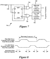
- a dead time interval is used between the on times so that both power transistors 106 and 108 are never conducting at the same time (see Figure 8 ).
- a signal may be provided in a microcontroller based application by a pulse width modulation (PWM) generator in combination with a clock, e.g., resistor capacitor (RC) oscillator.
- PWM pulse width modulation
- the PWM generator has the ability to generate digital signals with controllable variable frequency and duty cycle.
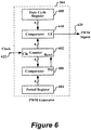
- the frequency of the PWM signal is adjusted by changing the value of a PWM period register, while the duty cycle is maintained at substantially fifty (50) percent by changing the value of a PWM duty register (see Figure 6 ).
- Florescent light ballast manufacturers require ultra high frequency resolution to provide smooth and accurate dimming control of the fluorescent lamps.
- the frequency step resolution of the PWM generator is a function of the input clock frequency thereto and the desired lamp excitation frequency.
- the PWM period register adjustment is not capable of producing small enough frequency steps for precise control of the lamp current (light intensity).
- PWM pulse width modulation
- a tuning register, OSCTUN, in combination with a RC oscillator may be used to create a precision variable frequency clock source that supplies a precision tunable clock frequency to a PWM generator that may be used in a fluorescent lamp dimming device for precision control of light intensity of a fluorescent lamp(s).
- the OSCTUN register can be used in these cases to provide fine frequency adjustment of the RC oscillator, which is the PWM generator clock source. For each value of the PWM period register, the OSCTUN register can be modified to provide one or more intermediate frequency adjustment steps.
- the RC oscillator output may optionally be connected to a PLL to increase the frequency of the PWM generator clock.
- a dimmable fluorescent lamp system having an electronic lighting ballast using pulse width modulation (PWM) to control the amount of light produced by a fluorescent lamp comprises: a clock oscillator capable of generating any one of a plurality of clock frequencies; a pulse width modulation (PWM) generator for generating a PWM signal, wherein the PWM generator receives a clock signal from the clock oscillator at the selected one of the plurality of clock frequencies; a circuit for converting the PWM signal to high and low drive signals; a first power switch controlled by the high drive signal; a second power switch controlled by the low drive signal; an inductor coupled to the first and second power switches, wherein the first power switch couples the inductor to a supply voltage, the second power switch couples the inductor to a supply voltage common, and the first and second power switches decouple the inductor from the supply voltage and supply voltage common, respectively; a direct current (DC) blocking capacitor coupled to the supply voltage common; a fluorescent lamp having first and second
- a method for controlling dimmable electronic lighting ballasts using pulse width modulation comprises the steps of: generating a clock signal having a frequency selected from a plurality of clock frequencies; and generating a pulse width modulation (PWM) signal having any one of a plurality of PWM signal frequencies, wherein the PWM signal is derived from the clock signal; wherein the PWM signal has course frequency steps are provided by period and duty cycle values of the PWM generator, and fine frequency steps are provided by selecting appropriate frequencies from the plurality of clock frequencies.
- PWM pulse width modulation
- a digital device for supplying a variable frequency pulse width modulation (PWM) signal for controlling light brightness of a fluorescent lamp comprises: a clock oscillator capable of generating any one of a plurality of clock frequencies; a pulse width modulation (PWM) generator for generating a PWM signal, wherein the PWM generator receives a clock signal from the clock oscillator at the selected one of the plurality of clock frequencies; and a circuit for converting the PWM signal to high and low drive signals; wherein course frequency steps of the PWM signal are provided by the PWM generator and fine frequency steps of the PWM signal are provided by selecting appropriate frequencies from the plurality of clock frequencies.
- PWM pulse width modulation
- a pulse width modulation technique for dimming a fluorescent lamp may be implemented by using an integrated circuit digital device, e.g ., microcontroller integrated circuit.
- an integrated circuit digital device e.g ., microcontroller integrated circuit.
- the PWM fluorescent lamp dimming circuit may comprise a digital device 502, high and low side drivers 510, a high-side power switching transistor 106, a low-side power switching transistor 108, an inductor 110, a fluorescent lamp 112, a filament capacitor 116, and a DC blocking capacitor 114.
- the power switching transistor drivers 510 may be used to translate the low output voltages from the digital device 502 to the high voltage levels required to operate the high side power switching transistor 106 and the low side power switching transistor 108.
- the digital device 502 may be used to switch the high-side driver ON or OFF, and the low-side drive OFF or On, respectively, of the power switching transistor drivers 510.
- the high-side power switching transistor 106 When the high-side drive is ON the high-side power switching transistor 106 allows current to flow through the resonant RLC fluorescent lamp circuit (inductor 110, fluorescent lamp 112 and DC blocking capacitor 114) in one direction, and when the low-side drive is ON the low-side power switching transistor 108 allows current to flow through the resonant RLC fluorescent lamp circuit (inductor 110, fluorescent lamp 112 and DC blocking capacitor 114) in the other direction.
- the high-side power switching transistor 106 and the low-side power switching transistor 108 cannot be both ON at the same time. Also a dead band is desirable, e.g., the high-side power switching transistor 106 and the low-side power switching transistor 108 are both OFF (see Figure 8 ).
- the digital device 502 may synthesize an alternating current (AC) signal by alternatively turning on the high-side and low-side outputs of the power switching transistor drivers 510. By carefully controlling the time duration of the high-side and low-side outputs of the power switching transistor drivers 510, AC power at selected frequencies is synthesized.
- the digital device 502 may comprise a microprocessor, a microcontroller, an application specific integrated circuit (ASIC), a programmable logic array (PLA), etc.
- the power switching transistors may be, for example but are not limited to, metal oxide field effect transistors (MOSFETs), insulated gate bipolar transistors (IGBTs), etc.
- the AC power at the specific frequencies generate an AC line voltage that is applied to the combination of the inductor 110, fluorescent lamp 112 and the DC blocking capacitor 114.
- the specific frequencies are selectable for initiating lamp gas ionization and controlling the current through the ionized gas, thereby controlling light intensity from the fluorescent lamp 112.
- the digital device 502 comprises a pulse width modulation (PWM) generator 504, a variable frequency clock 506 used as the timing signal for the PWM generator 504, and a variable frequency clock register 508 for storing digital representations of "veneer frequency" offsets of the variable frequency clock 506.
- PWM pulse width modulation
- the variable frequency clock 506 enables being able to use finer frequency granularity when selecting a power drive frequency to be generated by the PWM generator 504, as more fully described herein.
- the variable frequency clock 506 may comprise an resistor-capacitor (RC) oscillator or any other type of oscillator that may be tuned over a small range of frequencies.
- RC resistor-capacitor
- a timer/counter 602 counts up from zero until it reaches a value specified by a period register 604 as determined by a comparator 606.
- the counter 602 is incremented each time a clock signal 622 is received at the clock input of the counter 602.
- the period register 604 contains a user specified value which represents the maximum counter value that determines the PWM period.
- a duty cycle register 608 stores the user specified duty cycle value.
- the count value from the counter 602 is compared to the duty cycle value in the duty cycle register 608 with a comparator 610.
- the comparator 610 asserts a PWM output signal 620 (driven high) whenever the timer/counter 602 value is less than or equal to the duty cycle value stored in the duty cycle register 608, and when the timer/counter value 602 is greater than the duty cycle value stored in the duty cycle register 608, the PWM output signal 620 is de-asserted (driven low).
- a substantially fifty (50) percent duty cycle square wave over a wide range of frequencies can be generated for dimming control of the light intensity (brightness) from the fluorescent lamp 112.
- the clock signal 622 may be varied over a narrow range of frequencies so as to fine tune the PWM signal frequency between what is normally available between changes to the period value, as more fully described herein. This enables finer granularity of the PWM frequency so that there is more precise and smoother control when dimming the fluorescent lamp light intensity (brightness).
- the PWM frequency is the clock signal 622 frequency divided by the value in the period register.
- a corresponding value is loaded into the duty cycle register so that the PWM signal 620 has substantially a 50 percent duty cycle, e.g., on for about half of a PWM period and off for the other half of the PWM period.
- the PWM period is the reciprocal of the PWM frequency.
- the frequency of the PWM signal 620 is determined by the frequency of the clock signal 622 divided by the "period count value" stored in the period register 604. For example, using a clock frequency of 16 MHz and a period count value of 160 will produce a PWM signal 620 at a frequency of 100 KHz.
- Table I shows some of the PWM signal frequencies and associated period count values at a clock frequency of 16 MHz. Not every period count value is shown in Table I, but one having ordinary skill in the art of digital circuits in PWM generation and the benefit of this disclosure would readily understand that the period count value can be incremented or decremented by one (1).
- variable frequency clock 506 ( Figure 5 ) can be trimmed plus or minus in frequency through the variable frequency clock register 508.
- the digital device 502 is programmed to load period values into the period register 604 so as to generate a PWM signal 620 at frequencies determined by these period values and the frequency of the clock signal 622.
- the digital device 502 is also programmed to control the frequency of the variable frequency clock 506 through the variable frequency clock register 508 so as to increase the frequency granularity of the resulting PWM signal 620. This feature allows more precise and even control in dimming of the fluorescent lamp light intensity.
- the digital device 502 also is programmed to load appropriate duty cycle values into the duty cycle register 608 so as to maintain the duty cycle of the PWM signal at substantially fifty percent.
- Table I Clock - 16 MHz PWM Freq. (Hz) Period Register 100,000 160 88,888 180 80,000 200 76,190 210 74,419 215 74,074 216 73,733 217 73,394 218 73,059 219 72,727 220 71,111 225 69,565 230 66,666 240 61,538 260 57,143 280 53,333 300 50,000 320
- the frequency steps available from the PWM signal 620 are much finer in granularity and may change at about 48 Hz per step.
- This size frequency step change allows very smooth dimming control of fluorescent lamp light intensity according to the teachings of this disclosure. Modifying the tunable oscillator for even finer adjustment steps can further increase resolution without the need for high PWM frequencies. Therefore, it is contemplated and within the scope of this disclosure that other and further frequency step change sizes may be used according to the teachings of this disclosure.
- a range of clock frequencies are also contemplated herein, for example, in Table II above clock frequencies are shown to vary a little over plus or minus two (2) percent. Depending upon the number of bits of the PWM generator allowing a certain range of frequency step changes, the clock frequencies may be varied, but is not limited to, from about one (1) percent to about five (5) percent of the center frequency of the clock oscillator.
- FIG. 7 depicted is a schematic block diagram of a typical circuit for converting a square wave into two drive signals for turning on and off the power switching transistors 106 and 108 shown in Figure 5 .
- a flip-flop 730, and NOR gates 734 and 736 produce a high and a low output, respectively, that are mutually exclusive, i.e., when one is on and the other is off.
- a high-side power switching transistor interface 740 drives the gate of the high-side power switching transistor 106, and a low-side power switching transistor interface 738 drives the gate of the low-side power switching transistor 108.
- a typical waveform from the power switching transistor drivers 510 is shown in Figure 8 .
- the PLL comprises a voltage controlled oscillator (VCO) 902, an N-frequency divider 904, a frequency/phase detector 906, a tunable reference oscillator 910, and an oscillator tuning register 908.
- VCO voltage controlled oscillator
- the PLL may be used in generating a clock signal 622a for the PWM generator 504, and has the advantage that a higher frequency clock signal 622a may be generated from the lower frequency tunable reference oscillator 910.
- the reference oscillator 910 may be set to any one of a plurality of frequencies and the frequency selection is controlled from the oscillator tuning register 908.
- FIG 10 illustrates a schematic diagram of the fluorescent lamp circuit of Figure 5 further comprising a current sense resistor, according to still another specific example embodiment of this disclosure.
- a sense resistor 1016 is added to the circuit of Figure 5 , feedback control of the apparent brightness of the fluorescent lamp(s) may be implemented by measuring the current through the sense resistor 1016.
- the current through the sense resistor 1016 is substantially the same as the current through the lamp 112.
- the current through the sense resistor 1016 will produce a voltage across the sense resistor 1016 that is proportional to the lamp current. This voltage may be fed into an analog-to-digital converter (ADC) of the digital device 502a.
- ADC analog-to-digital converter
- PID control proportional-integral-differential
- a PID control loop may use this analog input representing fluorescent lamp brightness to adjust the lamp dimming circuit so as to deliver a consistent perceived lamp brightness level.
- the software program running on the digital device 502a may consider this as the demanded brightness level.
- a check of the current through the fluorescent lamp 112 will indicate the present apparent brightness of the fluorescent lamp 112. If the values don't agree, the dimming of the fluorescent lamp 112 may be adjusted up or down to increase or decrease the current through the fluorescent lamp 112. As the fluorescent lamp 112 increases or decreases in temperature because of its new brightness setting, the brightness may drift.
- the feedback control via the microcontroller's software program will maintain the demanded brightness regardless of temperature transitions (e.g., drift or transients) in the fluorescent lamp 112.
Landscapes
- Discharge-Lamp Control Circuits And Pulse- Feed Circuits (AREA)
Claims (15)
- Dimmbares Leuchtstofflampensystem, das ein elektronisches Vorschaltgerät aufweist, das Pulsweitenmodulation (PWM) zur Steuerung der von einer Leuchtstofflampe erzeugten Lichtmenge verwendet, wobei das System aufweist:einen Mikrocontroller (502; 502a), der einen abstimmbaren Taktoszillator (506) aufweist, der befähigt ist, jede einer Vielzahl von Taktfrequenzen zu erzeugen, und einen Impulsbreitenmodulations- (PWM-) Generator (504) zum Erzeugen eines PWM-Signals, wobei der PWM-Generator (504) bei der ausgewählten der Vielzahl von Taktfrequenzen ein Taktsignal vom Taktoszillator (506) empfängt;eine Schaltung (510) zum Umwandeln des PWM-Signals in hohe und niedrige Ansteuersignale;einen ersten Leistungsschalter (106), der durch das hohe Ansteuersignal gesteuert wird;einen zweiten Leistungsschalter (108), der durch das niedrige Ansteuersignal gesteuert wird;einen Induktor (110), der mit den ersten und zweiten Leistungsschaltern gekoppelt ist, wobei der erste Leistungsschalter (106) den Induktor (110) mit einer Versorgungsspannung koppelt, der zweite Leistungsschalter (108) den Induktor (110) mit einer gemeinsamen Versorgungsbezugsspannung koppelt, und die ersten und zweiten Leistungsschalter (106, 108) den Induktor (110) von der Versorgungsspannung bzw. der gemeinsamen Versorgungsbezugsspannung entkoppeln;einen Gleichstrom- (DC-) Sperrkondensator, der mit der gemeinsamen Versorgungsbezugsspannung gekoppelt ist;eine Leuchtstofflampe (112) mit ersten und zweiten Filamenten, wobei jedes Filament zwei Verbindungen aufweist, wobei eine erste Verbindung des ersten Filaments mit dem Induktor (110) und eine erste Verbindung des zweiten Filaments mit dem DC-Sperrkondensator (114) gekoppelt ist; undeinen Filamentkondensator (116), der eine zweite Verbindung des ersten Filaments mit einer zweiten Verbindung des zweiten Filaments der Leuchtstofflampe (110) koppelt;wobei der Mikrocontroller zum Steuern der von der Leuchtstofflampe erzeugten Lichtmenge so programmiert ist, dass er grobe Dimmschritte durch Steuerung des PWM-Generators und feine Dimmschritte durch Auswahl geeigneter Frequenzen aus der Vielzahl von Taktfrequenzen bereitstellt, wobei die ausgewählte aus der Vielzahl von Taktfrequenzen in einem Bereich liegt, in dem Strom durch die Leuchtstofflampe fließen kann, um Licht zu erzeugen.
- System gemäß Anspruch 1, wobei die ersten und zweiten Leistungsschalter (106, 108) erste bzw. zweite Leistungsschalttransistoren sind, vorzugsweise Metalloxidhalbleiter-Feldeffekttransistoren (MOSFETs) oder Bipolartransistoren mit isoliertem Gate (IGBTs).
- System gemäß Anspruch 1, wobei der Mikrocontroller (502; 502a) weiterhin ein Taktregister aufweist, das mit dem Taktoszillator gekoppelt ist und speichert, welche der Vielzahl von Taktfrequenzen vom Taktoszillator für die feine Dimmschritte erzeugt wird, und Perioden- und Arbeitszyklusregister für die groben Dimmschritte des PWM-Generators.
- System gemäß einem der vorhergehenden Ansprüche, das weiterhin einen Fluoreszenzlampenstrommesswiderstand (1016) aufweist, der zwischen dem DC-Sperrkondensator (114) und der gemeinsamen Versorgungsbezugsspannung gekoppelt ist, wobei der Fluoreszenzlampenstrommesswiderstand (1016) zur Messung des Leuchtstofflampenstroms verwendet wird.
- System gemäß Anspruch 4, wobei eine Spannung über dem Fluoreszenzlampenstrommesswiderstand (1016) mit einem analogen Eingang des Mikrocontrollers (502; 502a) gekoppelt ist, wobei der Mikrocontroller (502; 502a) die Spannung verwendet, um eine konstante Lichtintensität der Leuchtstofflampe (112) aufrechtzuerhalten.
- System gemäß einem der vorhergehenden Ansprüche, wobei der Taktoszillator (504) einen Phasenregelkreis (PLL) zum Erzeugen höherer Taktfrequenzen verwendet.
- System gemäß einem der vorhergehenden Ansprüche, wobei die Vielzahl von Taktfrequenzen plus oder minus von ungefähr einem (1) Prozent bis ungefähr fünf (5) Prozent einer Mittenfrequenz des Taktoszillators (504) aufweist.
- System gemäß Anspruch 7, wobei die Mittenfrequenz etwa 16 MHz beträgt.
- System gemäß einem der vorhergehenden Ansprüche, das weiterhin zweite und dritte Leistungsschalter aufweist, die als Vollbrückenleistungssteuerschaltung konfiguriert sind.
- Verfahren zum Steuern dimmbarer elektronischer Vorschaltgeräte für Leuchtstofflampen unter Verwendung einer Impulsbreitenmodulation (PWM) mit einem Mikrocontroller (502; 502a), der einen abstimmbaren Taktoszillator (506) aufweist, der eine einer Vielzahl von Taktfrequenzen erzeugen kann, und einen Pulsweitenmodulations- (PWM-) Generator (504) zum Erzeugen eines PWM-Signals, wobei der PWM-Generator (504) ein Taktsignal vom Taktoszillator (506) bei der ausgewählten der Vielzahl von Taktfrequenzen empfängt, wobei das Verfahren die Schritte des Programmierens des Mikrocontrollers aufweist:um mit einem Oszillator ein Taktsignal mit einer Frequenz zu erzeugen, die aus einer Vielzahl von Taktfrequenzen ausgewählt ist; undum ein Impulsbreitenmodulations- (PWM-) Signal zu erzeugen mit einem PWM-Generator, der eine einer Vielzahl von PWM-Signalfrequenzen aufweist, wobei das PWM-Signal aus dem Taktsignal abgeleitet wird;wobei, um die von der Leuchtstofflampe erzeugte Lichtmenge zu steuern, das PWM-Signal grobe Dimmschritte aufweist, die durch Perioden- und Arbeitszykluswerte des PWM-Generators bereitgestellt werden, und feine Dimmschritte, die durch Auswahl geeigneter Frequenzen aus der Vielzahl von Taktfrequenzen bereitgestellt werden, wobei die ausgewählte der Vielzahl von Taktfrequenzen innerhalb eines Bereichs liegt, in dem Strom durch die Leuchtstofflampe fließen kann, um Licht zu erzeugen.
- Verfahren oder System gemäß einem der vorhergehenden Ansprüche, wobei die PWM-Signalfrequenz zwischen ungefähr 50 kHz bis ungefähr 100 kHz variabel ist.
- Verfahren oder System gemäß einem der vorhergehenden Ansprüche, wobei die feinen Dimmschritte kleiner oder gleich etwa 60 Hz sind.
- Verfahren gemäß einem der vorhergehenden Ansprüche 10 bis 12, wobei das Taktsignal mit einem Phasenregelkreis- (PLL-) Oszillator erzeugt wird.
- Verfahren gemäß einem der vorhergehenden Ansprüche 10 bis 13, wobei die Vielzahl von Taktfrequenzen plus oder minus von ungefähr einem (1) Prozent bis ungefähr fünf (5) Prozent einer Mittenfrequenz des Taktsignals aufweist.
- Verfahren gemäß Anspruch 14, wobei die Mittenfrequenz etwa 16 MHz beträgt.
Applications Claiming Priority (3)
| Application Number | Priority Date | Filing Date | Title |
|---|---|---|---|
| US16865109P | 2009-04-13 | 2009-04-13 | |
| US12/748,881 US8698414B2 (en) | 2009-04-13 | 2010-03-29 | High resolution pulse width modulation (PWM) frequency control using a tunable oscillator |
| PCT/US2010/030729 WO2010120683A1 (en) | 2009-04-13 | 2010-04-12 | High resolution pulse width modulation (pwm) frequency control using a tunable oscillator |
Publications (2)
| Publication Number | Publication Date |
|---|---|
| EP2420111A1 EP2420111A1 (de) | 2012-02-22 |
| EP2420111B1 true EP2420111B1 (de) | 2020-08-19 |
Family
ID=42933831
Family Applications (1)
| Application Number | Title | Priority Date | Filing Date |
|---|---|---|---|
| EP10713786.1A Not-in-force EP2420111B1 (de) | 2009-04-13 | 2010-04-12 | Hochauflösende impulsbreitenmodulations-(pwm-) frequenzregelung unter verwendung eines abstimmbaren oszillators |
Country Status (6)
| Country | Link |
|---|---|
| US (1) | US8698414B2 (de) |
| EP (1) | EP2420111B1 (de) |
| KR (1) | KR101827544B1 (de) |
| CN (1) | CN102326456B (de) |
| TW (1) | TWI504315B (de) |
| WO (1) | WO2010120683A1 (de) |
Families Citing this family (15)
| Publication number | Priority date | Publication date | Assignee | Title |
|---|---|---|---|---|
| CN101926230B (zh) * | 2008-01-24 | 2014-02-19 | 奥斯兰姆有限公司 | 用于激励至少一个光源的电子镇流器和方法 |
| TWI479780B (zh) * | 2010-12-13 | 2015-04-01 | Hon Hai Prec Ind Co Ltd | 降壓轉換器 |
| US8558497B2 (en) * | 2011-07-15 | 2013-10-15 | Cypress Semiconductor Corporation | Reduced electromagnetic interference for pulse-width modulation |
| US8873616B2 (en) * | 2012-02-23 | 2014-10-28 | Microchip Technology Incorporated | High resolution pulse width modulator |
| TWI495236B (zh) * | 2012-12-21 | 2015-08-01 | System General Corp | 控制電路及控制方法 |
| US9006989B2 (en) * | 2012-12-26 | 2015-04-14 | Colorado Energy Research Technologies, LLC | Circuit for driving lighting devices |
| CN105898957A (zh) * | 2015-05-20 | 2016-08-24 | 深圳市光迹科技有限公司 | 一种通过可变频率pwm改善led调光性能的方法 |
| CN108207054B (zh) * | 2016-12-19 | 2021-08-24 | 上海莱狮半导体科技有限公司 | 负载的功率扩展电路和功率扩展方法 |
| WO2018185813A1 (ja) * | 2017-04-03 | 2018-10-11 | 東芝三菱電機産業システム株式会社 | 電力変換装置 |
| DE102017208361A1 (de) * | 2017-05-18 | 2018-11-22 | Robert Bosch Gmbh | Sensorvorrichtung |
| CN110677942B (zh) * | 2019-08-30 | 2025-07-25 | 北京临近空间飞行器系统工程研究所 | 调光装置,荧光显微光学系统和扫描及分析系统 |
| JP2021048523A (ja) * | 2019-09-19 | 2021-03-25 | 株式会社東芝 | Led駆動制御回路、電子回路及びled駆動制御方法 |
| JP2024505054A (ja) * | 2021-01-28 | 2024-02-02 | フィリップ・モーリス・プロダクツ・ソシエテ・アノニム | エアロゾル形成基体を加熱するための誘導加熱配設 |
| CN113933601B (zh) * | 2021-09-13 | 2023-09-15 | 北京车和家信息技术有限公司 | 脉宽调制信号采集方法、装置、计算机设备及存储介质 |
| CN116844496B (zh) * | 2022-03-24 | 2026-01-16 | 深圳和而泰小家电智能科技有限公司 | 一种调整液晶驱动的方法、装置以及存储介质 |
Citations (1)
| Publication number | Priority date | Publication date | Assignee | Title |
|---|---|---|---|---|
| US20080054825A1 (en) * | 2006-09-05 | 2008-03-06 | Microchip Technology Incorporated | Using Pulse Density Modulation for Controlling Dimmable Electronic Lighting Ballasts |
Family Cites Families (14)
| Publication number | Priority date | Publication date | Assignee | Title |
|---|---|---|---|---|
| US4942422A (en) * | 1987-05-22 | 1990-07-17 | Ricoh Company, Ltd. | Image reproducing device and transfer sheet used in the device |
| DE3912837A1 (de) * | 1989-04-19 | 1990-10-25 | Thomson Brandt Gmbh | Regelschaltung |
| US5420481A (en) * | 1993-09-27 | 1995-05-30 | Smiths Industries | Fluorescent lamp with wide range of luminous intensities |
| US6963178B1 (en) * | 1998-12-07 | 2005-11-08 | Systel Development And Industries Ltd. | Apparatus for controlling operation of gas discharge devices |
| US6750842B2 (en) * | 2002-04-24 | 2004-06-15 | Beyond Innovation Technology Co., Ltd. | Back-light control circuit of multi-lamps liquid crystal display |
| US6819011B2 (en) * | 2002-11-14 | 2004-11-16 | Fyre Storm, Inc. | Switching power converter controller with watchdog timer |
| CN101557670B (zh) * | 2003-02-06 | 2011-12-07 | 塔西软件开发有限及两合公司 | Lcd背光的数字控制系统 |
| US7098605B2 (en) * | 2004-01-15 | 2006-08-29 | Fairchild Semiconductor Corporation | Full digital dimming ballast for a fluorescent lamp |
| US7227317B2 (en) * | 2004-06-10 | 2007-06-05 | Atmel Corporation | Method and system for enhanced dimming resolution in a light ballast through use of multiple control frequencies |
| JP2006319399A (ja) * | 2005-05-10 | 2006-11-24 | Nec Electronics Corp | パルス幅変調回路及び多相クロック生成回路 |
| DE102005056229B4 (de) * | 2005-11-25 | 2014-11-20 | Diehl Aerospace Gmbh | Steuerschaltung sowie Verfahren zur Ansteuerung einer Gasentladungslampe |
| US8193719B2 (en) * | 2006-09-05 | 2012-06-05 | Microchip Technology Incorporated | Using pulse density modulation for controlling dimmable electronic lighting ballasts |
| US20100109549A1 (en) | 2007-02-06 | 2010-05-06 | Koninklijke Philips Electronics N.V. | Method and device for driving a gas discharge lamp |
| US8164367B1 (en) * | 2009-01-15 | 2012-04-24 | Integrated Device Technology, Inc. | Spread spectrum clock generation technique for imaging applications |
-
2010
- 2010-03-29 US US12/748,881 patent/US8698414B2/en active Active
- 2010-04-12 KR KR1020117019872A patent/KR101827544B1/ko not_active Expired - Fee Related
- 2010-04-12 WO PCT/US2010/030729 patent/WO2010120683A1/en not_active Ceased
- 2010-04-12 CN CN201080008841.7A patent/CN102326456B/zh not_active Expired - Fee Related
- 2010-04-12 EP EP10713786.1A patent/EP2420111B1/de not_active Not-in-force
- 2010-04-13 TW TW099111502A patent/TWI504315B/zh not_active IP Right Cessation
Patent Citations (1)
| Publication number | Priority date | Publication date | Assignee | Title |
|---|---|---|---|---|
| US20080054825A1 (en) * | 2006-09-05 | 2008-03-06 | Microchip Technology Incorporated | Using Pulse Density Modulation for Controlling Dimmable Electronic Lighting Ballasts |
Non-Patent Citations (2)
| Title |
|---|
| PRESSMAN, ABRAHAM I.: "Switching Power Supply Design", 1 January 1998, MCGRAW-HILL, ISBN: 0-07-052236-7, pages: 579 - 582 * |
| WEYDERT: "PWM with high precision required", 23 January 2010 (2010-01-23), Retrieved from the Internet <URL:http://www.microchip.com/forums/m472498.aspx> [retrieved on 20180323] * |
Also Published As
| Publication number | Publication date |
|---|---|
| WO2010120683A1 (en) | 2010-10-21 |
| CN102326456B (zh) | 2015-03-25 |
| KR101827544B1 (ko) | 2018-02-09 |
| US20100259179A1 (en) | 2010-10-14 |
| TW201043093A (en) | 2010-12-01 |
| US8698414B2 (en) | 2014-04-15 |
| KR20120013932A (ko) | 2012-02-15 |
| TWI504315B (zh) | 2015-10-11 |
| EP2420111A1 (de) | 2012-02-22 |
| CN102326456A (zh) | 2012-01-18 |
Similar Documents
| Publication | Publication Date | Title |
|---|---|---|
| EP2420111B1 (de) | Hochauflösende impulsbreitenmodulations-(pwm-) frequenzregelung unter verwendung eines abstimmbaren oszillators | |
| EP2080422B1 (de) | Modulation von impulsdichte zur steuerung von verdunkelbaren elektronischen beleuchungsvorschaltgeräten | |
| KR20030085043A (ko) | 고휘도 방전 램프용 조도조절 가능한 전자 안정기 | |
| US7728528B2 (en) | Electronic ballast with preheating and dimming control | |
| US20080136343A1 (en) | Resonant DC/AC inverter | |
| US6377000B2 (en) | Electronic ballast for gas discharge lamp | |
| EP1459608B1 (de) | Verfahren und vorrichtung zum steuern einer entladungslampe | |
| US8410719B2 (en) | Electronic ballast and method for controlling at least one light source | |
| US8193719B2 (en) | Using pulse density modulation for controlling dimmable electronic lighting ballasts | |
| US20110012536A1 (en) | Electronic ballast with dimming control from power line sensing | |
| KR101330658B1 (ko) | 조광장치를 구동하는 장치 | |
| TWI410175B (zh) | An electronic ballast that senses the brightness of the power line | |
| KR19980019980A (ko) | 안정기용 펄스 발생 회로 | |
| JP2003197394A (ja) | 放電灯点灯装置 | |
| JPH06140167A (ja) | 調光機能付きインバータ点灯回路 | |
| JPH03254099A (ja) | インバータ照明装置 | |
| EP1709843A1 (de) | Elektronische ballastschaltung mit stromrückkopplung mit mehreren steigungen | |
| JPH04249893A (ja) | 他励式インバータ点灯回路 | |
| KR20070093236A (ko) | 엘씨디 인버터 | |
| JPH02284383A (ja) | 放電灯点灯装置 |
Legal Events
| Date | Code | Title | Description |
|---|---|---|---|
| PUAI | Public reference made under article 153(3) epc to a published international application that has entered the european phase |
Free format text: ORIGINAL CODE: 0009012 |
|
| 17P | Request for examination filed |
Effective date: 20111109 |
|
| AK | Designated contracting states |
Kind code of ref document: A1 Designated state(s): AT BE BG CH CY CZ DE DK EE ES FI FR GB GR HR HU IE IS IT LI LT LU LV MC MK MT NL NO PL PT RO SE SI SK SM TR |
|
| DAX | Request for extension of the european patent (deleted) | ||
| 17Q | First examination report despatched |
Effective date: 20140730 |
|
| STAA | Information on the status of an ep patent application or granted ep patent |
Free format text: STATUS: EXAMINATION IS IN PROGRESS |
|
| GRAP | Despatch of communication of intention to grant a patent |
Free format text: ORIGINAL CODE: EPIDOSNIGR1 |
|
| STAA | Information on the status of an ep patent application or granted ep patent |
Free format text: STATUS: GRANT OF PATENT IS INTENDED |
|
| INTG | Intention to grant announced |
Effective date: 20200110 |
|
| GRAS | Grant fee paid |
Free format text: ORIGINAL CODE: EPIDOSNIGR3 |
|
| GRAA | (expected) grant |
Free format text: ORIGINAL CODE: 0009210 |
|
| STAA | Information on the status of an ep patent application or granted ep patent |
Free format text: STATUS: THE PATENT HAS BEEN GRANTED |
|
| AK | Designated contracting states |
Kind code of ref document: B1 Designated state(s): AT BE BG CH CY CZ DE DK EE ES FI FR GB GR HR HU IE IS IT LI LT LU LV MC MK MT NL NO PL PT RO SE SI SK SM TR |
|
| REG | Reference to a national code |
Ref country code: GB Ref legal event code: FG4D |
|
| REG | Reference to a national code |
Ref country code: CH Ref legal event code: EP |
|
| REG | Reference to a national code |
Ref country code: DE Ref legal event code: R096 Ref document number: 602010065212 Country of ref document: DE |
|
| REG | Reference to a national code |
Ref country code: AT Ref legal event code: REF Ref document number: 1305419 Country of ref document: AT Kind code of ref document: T Effective date: 20200915 |
|
| REG | Reference to a national code |
Ref country code: IE Ref legal event code: FG4D |
|
| REG | Reference to a national code |
Ref country code: LT Ref legal event code: MG4D |
|
| REG | Reference to a national code |
Ref country code: NL Ref legal event code: MP Effective date: 20200819 |
|
| PG25 | Lapsed in a contracting state [announced via postgrant information from national office to epo] |
Ref country code: FI Free format text: LAPSE BECAUSE OF FAILURE TO SUBMIT A TRANSLATION OF THE DESCRIPTION OR TO PAY THE FEE WITHIN THE PRESCRIBED TIME-LIMIT Effective date: 20200819 Ref country code: NO Free format text: LAPSE BECAUSE OF FAILURE TO SUBMIT A TRANSLATION OF THE DESCRIPTION OR TO PAY THE FEE WITHIN THE PRESCRIBED TIME-LIMIT Effective date: 20201119 Ref country code: PT Free format text: LAPSE BECAUSE OF FAILURE TO SUBMIT A TRANSLATION OF THE DESCRIPTION OR TO PAY THE FEE WITHIN THE PRESCRIBED TIME-LIMIT Effective date: 20201221 Ref country code: SE Free format text: LAPSE BECAUSE OF FAILURE TO SUBMIT A TRANSLATION OF THE DESCRIPTION OR TO PAY THE FEE WITHIN THE PRESCRIBED TIME-LIMIT Effective date: 20200819 Ref country code: LT Free format text: LAPSE BECAUSE OF FAILURE TO SUBMIT A TRANSLATION OF THE DESCRIPTION OR TO PAY THE FEE WITHIN THE PRESCRIBED TIME-LIMIT Effective date: 20200819 Ref country code: BG Free format text: LAPSE BECAUSE OF FAILURE TO SUBMIT A TRANSLATION OF THE DESCRIPTION OR TO PAY THE FEE WITHIN THE PRESCRIBED TIME-LIMIT Effective date: 20201119 Ref country code: GR Free format text: LAPSE BECAUSE OF FAILURE TO SUBMIT A TRANSLATION OF THE DESCRIPTION OR TO PAY THE FEE WITHIN THE PRESCRIBED TIME-LIMIT Effective date: 20201120 Ref country code: HR Free format text: LAPSE BECAUSE OF FAILURE TO SUBMIT A TRANSLATION OF THE DESCRIPTION OR TO PAY THE FEE WITHIN THE PRESCRIBED TIME-LIMIT Effective date: 20200819 |
|
| REG | Reference to a national code |
Ref country code: AT Ref legal event code: MK05 Ref document number: 1305419 Country of ref document: AT Kind code of ref document: T Effective date: 20200819 |
|
| PG25 | Lapsed in a contracting state [announced via postgrant information from national office to epo] |
Ref country code: PL Free format text: LAPSE BECAUSE OF FAILURE TO SUBMIT A TRANSLATION OF THE DESCRIPTION OR TO PAY THE FEE WITHIN THE PRESCRIBED TIME-LIMIT Effective date: 20200819 Ref country code: LV Free format text: LAPSE BECAUSE OF FAILURE TO SUBMIT A TRANSLATION OF THE DESCRIPTION OR TO PAY THE FEE WITHIN THE PRESCRIBED TIME-LIMIT Effective date: 20200819 Ref country code: NL Free format text: LAPSE BECAUSE OF FAILURE TO SUBMIT A TRANSLATION OF THE DESCRIPTION OR TO PAY THE FEE WITHIN THE PRESCRIBED TIME-LIMIT Effective date: 20200819 Ref country code: IS Free format text: LAPSE BECAUSE OF FAILURE TO SUBMIT A TRANSLATION OF THE DESCRIPTION OR TO PAY THE FEE WITHIN THE PRESCRIBED TIME-LIMIT Effective date: 20201219 |
|
| PG25 | Lapsed in a contracting state [announced via postgrant information from national office to epo] |
Ref country code: SM Free format text: LAPSE BECAUSE OF FAILURE TO SUBMIT A TRANSLATION OF THE DESCRIPTION OR TO PAY THE FEE WITHIN THE PRESCRIBED TIME-LIMIT Effective date: 20200819 Ref country code: RO Free format text: LAPSE BECAUSE OF FAILURE TO SUBMIT A TRANSLATION OF THE DESCRIPTION OR TO PAY THE FEE WITHIN THE PRESCRIBED TIME-LIMIT Effective date: 20200819 Ref country code: EE Free format text: LAPSE BECAUSE OF FAILURE TO SUBMIT A TRANSLATION OF THE DESCRIPTION OR TO PAY THE FEE WITHIN THE PRESCRIBED TIME-LIMIT Effective date: 20200819 Ref country code: DK Free format text: LAPSE BECAUSE OF FAILURE TO SUBMIT A TRANSLATION OF THE DESCRIPTION OR TO PAY THE FEE WITHIN THE PRESCRIBED TIME-LIMIT Effective date: 20200819 Ref country code: CZ Free format text: LAPSE BECAUSE OF FAILURE TO SUBMIT A TRANSLATION OF THE DESCRIPTION OR TO PAY THE FEE WITHIN THE PRESCRIBED TIME-LIMIT Effective date: 20200819 |
|
| REG | Reference to a national code |
Ref country code: DE Ref legal event code: R097 Ref document number: 602010065212 Country of ref document: DE |
|
| PG25 | Lapsed in a contracting state [announced via postgrant information from national office to epo] |
Ref country code: AT Free format text: LAPSE BECAUSE OF FAILURE TO SUBMIT A TRANSLATION OF THE DESCRIPTION OR TO PAY THE FEE WITHIN THE PRESCRIBED TIME-LIMIT Effective date: 20200819 Ref country code: ES Free format text: LAPSE BECAUSE OF FAILURE TO SUBMIT A TRANSLATION OF THE DESCRIPTION OR TO PAY THE FEE WITHIN THE PRESCRIBED TIME-LIMIT Effective date: 20200819 |
|
| PLBE | No opposition filed within time limit |
Free format text: ORIGINAL CODE: 0009261 |
|
| STAA | Information on the status of an ep patent application or granted ep patent |
Free format text: STATUS: NO OPPOSITION FILED WITHIN TIME LIMIT |
|
| PG25 | Lapsed in a contracting state [announced via postgrant information from national office to epo] |
Ref country code: SK Free format text: LAPSE BECAUSE OF FAILURE TO SUBMIT A TRANSLATION OF THE DESCRIPTION OR TO PAY THE FEE WITHIN THE PRESCRIBED TIME-LIMIT Effective date: 20200819 |
|
| 26N | No opposition filed |
Effective date: 20210520 |
|
| PG25 | Lapsed in a contracting state [announced via postgrant information from national office to epo] |
Ref country code: IT Free format text: LAPSE BECAUSE OF FAILURE TO SUBMIT A TRANSLATION OF THE DESCRIPTION OR TO PAY THE FEE WITHIN THE PRESCRIBED TIME-LIMIT Effective date: 20200819 |
|
| PGFP | Annual fee paid to national office [announced via postgrant information from national office to epo] |
Ref country code: DE Payment date: 20210323 Year of fee payment: 12 |
|
| PG25 | Lapsed in a contracting state [announced via postgrant information from national office to epo] |
Ref country code: SI Free format text: LAPSE BECAUSE OF FAILURE TO SUBMIT A TRANSLATION OF THE DESCRIPTION OR TO PAY THE FEE WITHIN THE PRESCRIBED TIME-LIMIT Effective date: 20200819 |
|
| PG25 | Lapsed in a contracting state [announced via postgrant information from national office to epo] |
Ref country code: MC Free format text: LAPSE BECAUSE OF FAILURE TO SUBMIT A TRANSLATION OF THE DESCRIPTION OR TO PAY THE FEE WITHIN THE PRESCRIBED TIME-LIMIT Effective date: 20200819 |
|
| GBPC | Gb: european patent ceased through non-payment of renewal fee |
Effective date: 20210412 |
|
| PG25 | Lapsed in a contracting state [announced via postgrant information from national office to epo] |
Ref country code: LU Free format text: LAPSE BECAUSE OF NON-PAYMENT OF DUE FEES Effective date: 20210412 |
|
| REG | Reference to a national code |
Ref country code: BE Ref legal event code: MM Effective date: 20210430 |
|
| PG25 | Lapsed in a contracting state [announced via postgrant information from national office to epo] |
Ref country code: CH Free format text: LAPSE BECAUSE OF NON-PAYMENT OF DUE FEES Effective date: 20210430 Ref country code: LI Free format text: LAPSE BECAUSE OF NON-PAYMENT OF DUE FEES Effective date: 20210430 Ref country code: GB Free format text: LAPSE BECAUSE OF NON-PAYMENT OF DUE FEES Effective date: 20210412 Ref country code: FR Free format text: LAPSE BECAUSE OF NON-PAYMENT OF DUE FEES Effective date: 20210430 |
|
| PG25 | Lapsed in a contracting state [announced via postgrant information from national office to epo] |
Ref country code: IE Free format text: LAPSE BECAUSE OF NON-PAYMENT OF DUE FEES Effective date: 20210412 |
|
| PG25 | Lapsed in a contracting state [announced via postgrant information from national office to epo] |
Ref country code: IS Free format text: LAPSE BECAUSE OF FAILURE TO SUBMIT A TRANSLATION OF THE DESCRIPTION OR TO PAY THE FEE WITHIN THE PRESCRIBED TIME-LIMIT Effective date: 20201219 |
|
| PG25 | Lapsed in a contracting state [announced via postgrant information from national office to epo] |
Ref country code: BE Free format text: LAPSE BECAUSE OF NON-PAYMENT OF DUE FEES Effective date: 20210430 |
|
| REG | Reference to a national code |
Ref country code: DE Ref legal event code: R119 Ref document number: 602010065212 Country of ref document: DE |
|
| PG25 | Lapsed in a contracting state [announced via postgrant information from national office to epo] |
Ref country code: DE Free format text: LAPSE BECAUSE OF NON-PAYMENT OF DUE FEES Effective date: 20221103 |
|
| PG25 | Lapsed in a contracting state [announced via postgrant information from national office to epo] |
Ref country code: HU Free format text: LAPSE BECAUSE OF FAILURE TO SUBMIT A TRANSLATION OF THE DESCRIPTION OR TO PAY THE FEE WITHIN THE PRESCRIBED TIME-LIMIT; INVALID AB INITIO Effective date: 20100412 Ref country code: CY Free format text: LAPSE BECAUSE OF FAILURE TO SUBMIT A TRANSLATION OF THE DESCRIPTION OR TO PAY THE FEE WITHIN THE PRESCRIBED TIME-LIMIT Effective date: 20200819 |
|
| PG25 | Lapsed in a contracting state [announced via postgrant information from national office to epo] |
Ref country code: MK Free format text: LAPSE BECAUSE OF FAILURE TO SUBMIT A TRANSLATION OF THE DESCRIPTION OR TO PAY THE FEE WITHIN THE PRESCRIBED TIME-LIMIT Effective date: 20200819 |
|
| PG25 | Lapsed in a contracting state [announced via postgrant information from national office to epo] |
Ref country code: MT Free format text: LAPSE BECAUSE OF FAILURE TO SUBMIT A TRANSLATION OF THE DESCRIPTION OR TO PAY THE FEE WITHIN THE PRESCRIBED TIME-LIMIT Effective date: 20200819 |
|
| PG25 | Lapsed in a contracting state [announced via postgrant information from national office to epo] |
Ref country code: TR Free format text: LAPSE BECAUSE OF FAILURE TO SUBMIT A TRANSLATION OF THE DESCRIPTION OR TO PAY THE FEE WITHIN THE PRESCRIBED TIME-LIMIT Effective date: 20200819 |