EP2078208B1 - Tamper respondent sensor and enclosure - Google Patents
Tamper respondent sensor and enclosure Download PDFInfo
- Publication number
- EP2078208B1 EP2078208B1 EP07852722.3A EP07852722A EP2078208B1 EP 2078208 B1 EP2078208 B1 EP 2078208B1 EP 07852722 A EP07852722 A EP 07852722A EP 2078208 B1 EP2078208 B1 EP 2078208B1
- Authority
- EP
- European Patent Office
- Prior art keywords
- substrate
- layer
- article
- conductive traces
- respondent sensor
- Prior art date
- Legal status (The legal status is an assumption and is not a legal conclusion. Google has not performed a legal analysis and makes no representation as to the accuracy of the status listed.)
- Not-in-force
Links
Images

Classifications
-
- G—PHYSICS
- G08—SIGNALLING
- G08B—SIGNALLING OR CALLING SYSTEMS; ORDER TELEGRAPHS; ALARM SYSTEMS
- G08B13/00—Burglar, theft or intruder alarms
- G08B13/02—Mechanical actuation
- G08B13/12—Mechanical actuation by the breaking or disturbance of stretched cords or wires
- G08B13/126—Mechanical actuation by the breaking or disturbance of stretched cords or wires for a housing, e.g. a box, a safe, or a room
- G08B13/128—Mechanical actuation by the breaking or disturbance of stretched cords or wires for a housing, e.g. a box, a safe, or a room the housing being an electronic circuit unit, e.g. memory or CPU chip
-
- G—PHYSICS
- G06—COMPUTING OR CALCULATING; COUNTING
- G06F—ELECTRIC DIGITAL DATA PROCESSING
- G06F21/00—Security arrangements for protecting computers, components thereof, programs or data against unauthorised activity
- G06F21/70—Protecting specific internal or peripheral components, in which the protection of a component leads to protection of the entire computer
- G06F21/86—Secure or tamper-resistant housings
- G06F21/87—Secure or tamper-resistant housings by means of encapsulation, e.g. for integrated circuits
-
- H—ELECTRICITY
- H05—ELECTRIC TECHNIQUES NOT OTHERWISE PROVIDED FOR
- H05K—PRINTED CIRCUITS; CASINGS OR CONSTRUCTIONAL DETAILS OF ELECTRIC APPARATUS; MANUFACTURE OF ASSEMBLAGES OF ELECTRICAL COMPONENTS
- H05K1/00—Printed circuits
- H05K1/02—Details
- H05K1/0275—Security details, e.g. tampering prevention or detection
-
- G—PHYSICS
- G06—COMPUTING OR CALCULATING; COUNTING
- G06F—ELECTRIC DIGITAL DATA PROCESSING
- G06F2221/00—Indexing scheme relating to security arrangements for protecting computers, components thereof, programs or data against unauthorised activity
- G06F2221/21—Indexing scheme relating to G06F21/00 and subgroups addressing additional information or applications relating to security arrangements for protecting computers, components thereof, programs or data against unauthorised activity
- G06F2221/2101—Auditing as a secondary aspect
-
- H—ELECTRICITY
- H05—ELECTRIC TECHNIQUES NOT OTHERWISE PROVIDED FOR
- H05K—PRINTED CIRCUITS; CASINGS OR CONSTRUCTIONAL DETAILS OF ELECTRIC APPARATUS; MANUFACTURE OF ASSEMBLAGES OF ELECTRICAL COMPONENTS
- H05K1/00—Printed circuits
- H05K1/02—Details
- H05K1/03—Use of materials for the substrate
- H05K1/0393—Flexible materials
-
- H—ELECTRICITY
- H05—ELECTRIC TECHNIQUES NOT OTHERWISE PROVIDED FOR
- H05K—PRINTED CIRCUITS; CASINGS OR CONSTRUCTIONAL DETAILS OF ELECTRIC APPARATUS; MANUFACTURE OF ASSEMBLAGES OF ELECTRICAL COMPONENTS
- H05K2201/00—Indexing scheme relating to printed circuits covered by H05K1/00
- H05K2201/05—Flexible printed circuits [FPCs]
- H05K2201/056—Folded around rigid support or component
-
- H—ELECTRICITY
- H05—ELECTRIC TECHNIQUES NOT OTHERWISE PROVIDED FOR
- H05K—PRINTED CIRCUITS; CASINGS OR CONSTRUCTIONAL DETAILS OF ELECTRIC APPARATUS; MANUFACTURE OF ASSEMBLAGES OF ELECTRICAL COMPONENTS
- H05K2201/00—Indexing scheme relating to printed circuits covered by H05K1/00
- H05K2201/10—Details of components or other objects attached to or integrated in a printed circuit board
- H05K2201/10007—Types of components
- H05K2201/10151—Sensor
Definitions
- This invention relates to tamper respondent enclosures, and in particular, to a sensor used as a tamper respondent enclosure.
- Tamper respondent enclosures are used in various applications, including the transport of sensitive information and protecting electronic devices.
- Typical enclosures are in the form of envelopes and shallow boxes, the walls of which are formed by folding flexible sheets incorporating tamper detection features.
- sheets incorporating tamper detection features are known as "sensors”. These sheets may also be wrapped around preexisting boxes or enclosures.
- Such sheets include layers of flexible material and a matrix of diagonally extending or zig-zag pattern semi-conductive or conductive lines, also known as conductive traces.
- the lines or traces are printed on thin insulating film.
- the matrix of lines forms a continuous conductor which is broken if attempts are made to penetrate the film.
- the sensor matrix is monitored and when a tamper occurs the electrical state of the sensor changes. A detection of a change in state can initiate a signal. This signal can erase information stored within the enclosure, or otherwise protect the information from being discovered.
- the matrix of semi-conductive or conductive lines or traces on the insulating film is printed on both sides of the film.
- the lines on one side are disposed in the sections of the film opposite from where the lines are disposed on the opposite side. In this manner, complete coverage of the film is obtained, and it is more difficult to penetrate the film without cutting a line, either on one side of the film or the other.
- the flexible material is a clear insulating film such as PET.
- known methods include a potting material.
- This potting material is typically a dark resin that encapsulates the entire film. The dark potting material provides a mechanical barrier and hides the location of the semi-conductive lines.
- WO 2004/037660 (Peterson, et al. ) teaches a tamper detection system which can be formed from a blank.
- the present invention provides a tamper respondent sensor according to claim 1.
- the substrate is insulating and made of an opaque film such as PET, and the first layer is adjacent the enclosure.
- the substrate and enclosure further include an opening for communication between the circuit board and an external device.
- the external device is a computer mother board, a connector, and a cable.
- the circuit board in an alternative embodiment includes a wireless transmitter.
- the tamper respondent sensor is shaped to allow only two layers at the at least one overlap region, and the second side of said substrate has no exposed conductive traces.
- the substrate further includes an adhesive disposed over the first layer of conductive traces.
- the adhesive is preferably a pressure sensitive adhesive (PSA).
- the tamper respondent sensor preferably further includes an input/output (I/O) lead.
- I/O input/output
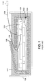
- FIG 1 is a schematic diagram of a prior art tamper respondent enclosure.
- Circuit board 100 has components 101 disposed thereon. Components 101 contain the sensitive information that is desired to be protected.
- a box or enclosure 102 surrounds circuit board 100 and components 101.
- Enclosure 102 has a sensor 103 disposed around it.
- Sensor 103 comprises a clear PET substrate 104.
- On both sides of PET substrate 104 are disposed printed traces 105. This is a matrix of conductive lines on each side. The lines are disposed in offsetting relation from one side to the other to ensure complete coverage of PET substrate 104.
- the inside of PET substrate 104 also has a layer of adhesive 106 disposed over the printed trace 105 on that surface.
- Adhesive layer 106 is a pressure sensitive adhesive (PSA).
- PSA pressure sensitive adhesive
- the entire sensor is then encapsulated in an opaque encapsulant or potting material 107.
- Potting material 107 helps obfuscate printed traces 105.
- An outer shell 108 surrounds the device.
- a cable 109 is used to connect components 101 with exterior components 110.
- the top section of sensor 103 is shown to be open, this is for illustration purposes only. In use, the overlapping ends of sensor 103 are secured to one another by adhesive layer 106.
- this device includes the deposition of printed traces on two sides of the PET substrate and it also includes the potting layer 107.
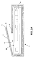
- FIG. 2A is a schematic representation of an exemplary embodiment of the present invention.
- a circuit board 20 has components 21 disposed thereon. Components 21 contain sensitive information to be protected.
- circuit board 20 can include wireless transmitters as components 21.
- Circuit board 20 and components 21 are enclosed by a box or enclosure 22.
- Enclosure 22 may be any shape. A rectangular shape is shown in this embodiment, but it may also be trapezoidal, wedge-shaped, or any other shape.
- Enclosure 22 is encapsulated by tamper respondent sensor 10.
- tamper respondent sensor 10 may be wrapped around a circuit board without a preexisting box or enclosure, in which case a filler may be used to form a surface over the circuit board to which tamper respondent sensor 10 adheres.
- Tamper respondent sensor 10 includes a substrate 11.
- substrate 11 an insulating material such as PET.
- substrate 11 is opaque. By using an opaque PET for substrate 11, it is not necessary to subsequently pot the material in order to obfuscate the printed traces.
- Substrate 11 has a first side 12 and second side 13.
- First side 12 is the inside of the substrate as illustrated in Figure 2A .
- Disposed on this first side 12 is a first layer of conductive traces 14.
- the conductive traces are made of a conductive, non-metallic ink, such as carbon-loaded polymer resin as taught, for example, in U.S. Patent No. 5,539,379 .
- Other materials known in the art may be used for the traces.
- Substrate 11 is adapted to be folded to produce an overlapping portion of first side 12 with an overlapping portion of second side 13.
- second side 13 which is the outer side of substrate 11 in the illustrated embodiment, a second layer of conductive traces 15 is disposed.
- Second layer of conductive traces 15 is present, however, only at the overlapping portion of second side 13. That is, second layer of conductive traces 15 is only disposed on that portion of second side 13 where there is an overlap with first side 12.
- the remainder of second side 13 is a region free of conductive traces. Thus, there are no exposed traces on second side 13.
- the traces on second side 13 are electrically connected to the traces on first side 12, for example by a via.
- the vias are located at the overlapping portion.
- a monitor (not shown) detects the circuit completed by first layer of conductive traces 14 and second layer of conductive traces 15 and monitors the electrical state. If this electrical state changes, indicating that the circuit has been broken, for example by cutting one of the traces, the monitor can trigger a response such as erasing information stored in components 21.
- the overlap region is open for purposes of illustration.
- the overlap is mated such that second layer of conductive traces 15 is adhered to first layer of conductive traces 14 by an adhesive layer 30.
- Adhesive layer 30 is preferably a tackifier, such as a PSA.
- Adhesive layer 30 is disposed on first side 12 of substrate 11 on the first layer of conductive traces 14. In this manner, once mated, if someone tries to tamper with sensor 10, by lifting substrate 11 at the overlap, adhesive layer 30 will sever either first layer of conductive traces 14 or second layer of conductive traces 15, thereby causing an interruption in the signal and triggering erasure or other protection of information stored in components 21 as described above.
- a cable 71 is used to connect components inside the device to components outside the device.
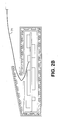
- Figure 3A and Figure 3B show alternative embodiments of the present invention.
- the embodiments represents a sensor 10 for use in wrapping an enclosure of a rectangular shape ( Figure 3A ) and a wedge shape ( Figure 3B ).
- the portion of Figures 3A and 3B labeled “unwrapped” shows sensor 10 in its intermediate form. Once an enclosure is placed on sensor 10, sensor 10 is then wrapped around the enclosure to completely encapsulate it, as illustrated in the portion of the figures labeled "wrapped.”
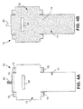
- FIG 4A is a bottom view of an exemplary sensor 10 according to the present invention.
- Figure 4B is a top view of sensor 10.
- sensor 10 includes substrate 11.
- substrate 11 is an opaque film such as PET.
- First side 12 of substrate 11 has first layer of conductive traces 14 disposed thereon.
- traces 14 are disposed in an unpredictable pattern on substrate 11. This is in contrast to diagonal (zig-zag), straight, or sinusoidal wave trace lines known in the art. Because these known patterns repeat at regular intervals, it potentially makes the sensor vulnerable to a jumper attack wherein the attacker can locate two points of the same trace and bypass the trace with a conductive jumper. Potentially, the attacker can then penetrate the sensor without triggering a change in electrical state.
- the trace herein is manually drawn using computer-aided software packages such as PCB-PADS ® , from Mentor Graphics, a printed circuit board layout software program.
- a second layer of conductive traces 15 is disposed on the portions of second side 13 of substrate 11 that will overlap with first side 12 as described above.
- the remainder of second side 13 is a region free of conductive traces. Thus, there are no exposed traces on second side 13 once it is wrapped around an enclosure.
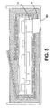
- FIG. 4A and 4B Also shown in Figures 4A and 4B is an opening 20 in sensor 10 which is preferably included in sensor 10 to allow mating of a circuit board 20 with another device external to sensor 10.
- the external device can be a computer mother board, a connector, or a cable, for example.
- Fig. 5 illustrates an exemplary embodiment wherein opening 20 allows mating of component 21 to a connector 80.
- an I/O lead 40 extending from substrate 11.
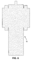
- Fig. 6 is a top view of exemplary sensor 10 without opening 20. This sensor 10 of Fig. 6 would be connected using a cable through the overlap zone as shown in Fig. 2B .
- the present invention provides distinctive advantages over the known art. Specifically, employing an unpredictable pattern for the traces makes it more difficult to defeat the device. In addition, using an opaque PET for substrate 11 obviates the need to pot the sensor. This eliminates a processing step, making production more efficient and cost effective. It also provides natural obfuscation for the conductive traces which may render the use of a second layer of conductive traces over the entire second side 13 of substrate 11 unnecessary. This also eliminates processing steps increasing efficiency and reducing costs. By selectively putting the second layer of conductive traces 15 only at portions of the second side 13 where substrate 11 overlaps, an effective tamper respondent enclosure is produced.
- relatively small overlapping portions are depicted.
- larger overlapping portions are used, for example covering an entire side of box 22 or furthermore all sides of a box.
Landscapes
- Engineering & Computer Science (AREA)
- Computer Hardware Design (AREA)
- General Engineering & Computer Science (AREA)
- Physics & Mathematics (AREA)
- General Physics & Mathematics (AREA)
- Microelectronics & Electronic Packaging (AREA)
- Computer Security & Cryptography (AREA)
- Theoretical Computer Science (AREA)
- Software Systems (AREA)
- Structure Of Printed Boards (AREA)
- Burglar Alarm Systems (AREA)
- Measurement Of The Respiration, Hearing Ability, Form, And Blood Characteristics Of Living Organisms (AREA)
Applications Claiming Priority (2)
| Application Number | Priority Date | Filing Date | Title |
|---|---|---|---|
| US11/592,766 US7760086B2 (en) | 2006-11-03 | 2006-11-03 | Tamper respondent sensor and enclosure |
| PCT/US2007/021881 WO2008063320A2 (en) | 2006-11-03 | 2007-10-11 | Tamper respondent sensor and enclosure |
Publications (3)
| Publication Number | Publication Date |
|---|---|
| EP2078208A2 EP2078208A2 (en) | 2009-07-15 |
| EP2078208A4 EP2078208A4 (en) | 2010-11-03 |
| EP2078208B1 true EP2078208B1 (en) | 2013-12-11 |
Family
ID=39359265
Family Applications (1)
| Application Number | Title | Priority Date | Filing Date |
|---|---|---|---|
| EP07852722.3A Not-in-force EP2078208B1 (en) | 2006-11-03 | 2007-10-11 | Tamper respondent sensor and enclosure |
Country Status (4)
| Country | Link |
|---|---|
| US (1) | US7760086B2 (enExample) |
| EP (1) | EP2078208B1 (enExample) |
| JP (1) | JP5600007B2 (enExample) |
| WO (1) | WO2008063320A2 (enExample) |
Families Citing this family (53)
| Publication number | Priority date | Publication date | Assignee | Title |
|---|---|---|---|---|
| US7414858B2 (en) | 2002-04-11 | 2008-08-19 | Koninklijke Philips Electronics N.V. | Method of manufacturing an electronic device |
| GB2412996B (en) * | 2004-04-08 | 2008-11-12 | Gore & Ass | Tamper respondent covering |
| US7640658B1 (en) * | 2005-10-18 | 2010-01-05 | Teledyne Technologies Incorporated | Methods for forming an anti-tamper pattern |
| FR2933798A1 (fr) * | 2008-07-11 | 2010-01-15 | Pierre Jean Merce | Dispositif de securite destine a surveiller l'accessibilite a un objet |
| DE102009002559A1 (de) * | 2009-04-22 | 2010-10-28 | Robert Bosch Gmbh | Sensoranordnung |
| US20130265163A1 (en) * | 2010-06-09 | 2013-10-10 | Raytheon Company | Magnetic Field Activated Intrusion Detection |
| AU2012220340A1 (en) * | 2011-02-22 | 2013-08-22 | Joelmar Pty Ltd | Survival and location enhancement garment and headgear |
| GB2504478A (en) * | 2012-07-27 | 2014-02-05 | Johnson Electric Sa | Security Wrap Film for Protecting Electronic Device |
| GB2515996A (en) * | 2013-04-15 | 2015-01-14 | Johnson Electric Sa | Security wrap with tearable substrate |
| US9521764B2 (en) * | 2013-12-09 | 2016-12-13 | Timothy Steiner | Tamper respondent apparatus |
| JP6327054B2 (ja) * | 2014-01-08 | 2018-05-23 | セイコーエプソン株式会社 | フィスカルプリンター |
| US9392734B1 (en) | 2014-02-11 | 2016-07-12 | Lockheed Martin Corporation | Security wrapper for an electronic assembly and methods for forming such a wrapper |
| US10579833B1 (en) | 2014-12-16 | 2020-03-03 | Thales Esecurity, Inc. | Tamper detection circuit assemblies and related manufacturing processes |
| US9560737B2 (en) * | 2015-03-04 | 2017-01-31 | International Business Machines Corporation | Electronic package with heat transfer element(s) |
| US10426037B2 (en) | 2015-07-15 | 2019-09-24 | International Business Machines Corporation | Circuitized structure with 3-dimensional configuration |
| US10175064B2 (en) | 2015-09-25 | 2019-01-08 | International Business Machines Corporation | Circuit boards and electronic packages with embedded tamper-respondent sensor |
| US9911012B2 (en) | 2015-09-25 | 2018-03-06 | International Business Machines Corporation | Overlapping, discrete tamper-respondent sensors |
| US10098235B2 (en) | 2015-09-25 | 2018-10-09 | International Business Machines Corporation | Tamper-respondent assemblies with region(s) of increased susceptibility to damage |
| US9578764B1 (en) | 2015-09-25 | 2017-02-21 | International Business Machines Corporation | Enclosure with inner tamper-respondent sensor(s) and physical security element(s) |
| US9591776B1 (en) | 2015-09-25 | 2017-03-07 | International Business Machines Corporation | Enclosure with inner tamper-respondent sensor(s) |
| US9924591B2 (en) | 2015-09-25 | 2018-03-20 | International Business Machines Corporation | Tamper-respondent assemblies |
| US9894749B2 (en) * | 2015-09-25 | 2018-02-13 | International Business Machines Corporation | Tamper-respondent assemblies with bond protection |
| US10172239B2 (en) | 2015-09-25 | 2019-01-01 | International Business Machines Corporation | Tamper-respondent sensors with formed flexible layer(s) |
| US10143090B2 (en) | 2015-10-19 | 2018-11-27 | International Business Machines Corporation | Circuit layouts of tamper-respondent sensors |
| US9978231B2 (en) | 2015-10-21 | 2018-05-22 | International Business Machines Corporation | Tamper-respondent assembly with protective wrap(s) over tamper-respondent sensor(s) |
| US9913389B2 (en) * | 2015-12-01 | 2018-03-06 | International Business Corporation Corporation | Tamper-respondent assembly with vent structure |
| US10327343B2 (en) | 2015-12-09 | 2019-06-18 | International Business Machines Corporation | Applying pressure to adhesive using CTE mismatch between components |
| US9555606B1 (en) | 2015-12-09 | 2017-01-31 | International Business Machines Corporation | Applying pressure to adhesive using CTE mismatch between components |
| DE102015122000B4 (de) * | 2015-12-16 | 2019-02-07 | Fujitsu Client Computing Limited | Anordnung und elektronisches Gerät |
| US9554477B1 (en) | 2015-12-18 | 2017-01-24 | International Business Machines Corporation | Tamper-respondent assemblies with enclosure-to-board protection |
| US9887847B2 (en) | 2016-02-03 | 2018-02-06 | International Business Machines Corporation | Secure crypto module including conductor on glass security layer |
| US9916744B2 (en) | 2016-02-25 | 2018-03-13 | International Business Machines Corporation | Multi-layer stack with embedded tamper-detect protection |
| JP6613955B2 (ja) * | 2016-02-26 | 2019-12-04 | 沖電気工業株式会社 | 入力装置および自動取引装置 |
| US9904811B2 (en) | 2016-04-27 | 2018-02-27 | International Business Machines Corporation | Tamper-proof electronic packages with two-phase dielectric fluid |
| US9913370B2 (en) | 2016-05-13 | 2018-03-06 | International Business Machines Corporation | Tamper-proof electronic packages formed with stressed glass |
| US9881880B2 (en) | 2016-05-13 | 2018-01-30 | International Business Machines Corporation | Tamper-proof electronic packages with stressed glass component substrate(s) |
| US9858776B1 (en) | 2016-06-28 | 2018-01-02 | International Business Machines Corporation | Tamper-respondent assembly with nonlinearity monitoring |
| US10321589B2 (en) | 2016-09-19 | 2019-06-11 | International Business Machines Corporation | Tamper-respondent assembly with sensor connection adapter |
| US10299372B2 (en) | 2016-09-26 | 2019-05-21 | International Business Machines Corporation | Vented tamper-respondent assemblies |
| US10271424B2 (en) | 2016-09-26 | 2019-04-23 | International Business Machines Corporation | Tamper-respondent assemblies with in situ vent structure(s) |
| US9999124B2 (en) * | 2016-11-02 | 2018-06-12 | International Business Machines Corporation | Tamper-respondent assemblies with trace regions of increased susceptibility to breaking |
| US10327329B2 (en) | 2017-02-13 | 2019-06-18 | International Business Machines Corporation | Tamper-respondent assembly with flexible tamper-detect sensor(s) overlying in-situ-formed tamper-detect sensor |
| US10157527B1 (en) | 2017-11-28 | 2018-12-18 | International Business Machines Corporation | Embossed printed circuit board for intrusion detection |
| CN108260280B (zh) * | 2017-12-04 | 2020-12-01 | 深圳市新宇腾跃电子有限公司 | 一种fpc折弯成型工艺 |
| US10306753B1 (en) * | 2018-02-22 | 2019-05-28 | International Business Machines Corporation | Enclosure-to-board interface with tamper-detect circuit(s) |
| US11122682B2 (en) | 2018-04-04 | 2021-09-14 | International Business Machines Corporation | Tamper-respondent sensors with liquid crystal polymer layers |
| EP3550623B1 (en) | 2018-04-06 | 2020-07-29 | Fraunhofer-Gesellschaft zur Förderung der angewandten Forschung e.V. | Puf-film and method for producing the same |
| EP3550475A1 (en) | 2018-04-06 | 2019-10-09 | Fraunhofer-Gesellschaft zur Förderung der angewandten Forschung e.V. | Puf-film and method for producing the same |
| EP3550466B1 (en) | 2018-04-06 | 2023-08-02 | Fraunhofer-Gesellschaft zur Förderung der angewandten Forschung e.V. | Puf-film and method for producing the same |
| US11191154B2 (en) | 2018-06-13 | 2021-11-30 | International Business Machines Corporation | Enclosure with tamper respondent sensor |
| US11089675B2 (en) | 2018-10-22 | 2021-08-10 | Te Connectivity Corporation | Tamper sensor |
| WO2022104099A1 (en) * | 2020-11-12 | 2022-05-19 | Jumbe Nelson L | Transducers, their methods of manufacture and uses |
| TWI810049B (zh) * | 2022-08-31 | 2023-07-21 | 緯穎科技服務股份有限公司 | 伺服器及儲存模組 |
Family Cites Families (34)
| Publication number | Priority date | Publication date | Assignee | Title |
|---|---|---|---|---|
| US3644825A (en) * | 1969-12-31 | 1972-02-22 | Texas Instruments Inc | Magnetic detection system for detecting movement of an object utilizing signals derived from two orthogonal pickup coils |
| US4188549A (en) * | 1977-11-11 | 1980-02-12 | Federal Screw Works | Acoustically responsive sensor switch |
| US4325089A (en) * | 1979-12-10 | 1982-04-13 | Hsu Da L | System for safeguarding magnetically recorded data |
| US4593384A (en) * | 1984-12-21 | 1986-06-03 | Ncr Corporation | Security device for the secure storage of sensitive data |
| GB8814471D0 (en) | 1988-06-17 | 1988-07-20 | Gore & Ass | Security enclosure |
| GB9113455D0 (en) | 1991-06-21 | 1991-08-07 | Gore W L & Ass Uk | Improvements in security enclosures |
| GB9113437D0 (en) | 1991-06-21 | 1991-08-07 | Gore W L & Ass Uk | Improvements in security enclosures |
| GB9113436D0 (en) | 1991-06-21 | 1991-08-07 | Gore W L & Ass Uk | Improvements in security enclosures |
| GB9115972D0 (en) | 1991-07-24 | 1991-09-11 | Gore W L & Ass Uk | Improvements in security enclosures |
| US6215397B1 (en) * | 1996-08-13 | 2001-04-10 | Lindskog Innovation Ab | Electrical manually portable security case for the storage of theft attractive articles with an electrical mat having at least one elongated electrically conductive wire in a substantially continuous mesh, loop or eye structure |
| GB2270785B (en) | 1992-09-22 | 1996-05-08 | Gore & Ass | Improvements in security enclosure manufacture |
| GB2275914B (en) * | 1993-03-12 | 1997-01-29 | Gore & Ass | Tamper respondent enclosure |
| US5832772A (en) * | 1995-01-27 | 1998-11-10 | The Regents Of The University Of California | Micropower RF material proximity sensor |
| US5910774A (en) * | 1996-09-18 | 1999-06-08 | Itron, Inc. | Sensor for count and tamper detection |
| DE19738990C2 (de) | 1997-09-05 | 1999-11-25 | Siemens Ag | Einrichtung zum Schutz gegen Mißbrauch einer Chipkarte |
| GB9721932D0 (en) | 1997-10-17 | 1997-12-17 | Gore W L & Ass Uk | Tamper respondent enclosure |
| US6496119B1 (en) * | 1998-11-05 | 2002-12-17 | Infineon Technologies Ag | Protection circuit for an integrated circuit |
| WO2000045592A1 (en) * | 1999-01-29 | 2000-08-03 | Hamamatsu Photonics K.K. | Photodetector device |
| US6396400B1 (en) * | 1999-07-26 | 2002-05-28 | Epstein, Iii Edwin A. | Security system and enclosure to protect data contained therein |
| CN1246730A (zh) | 1999-09-13 | 2000-03-08 | 后健慈 | 集成电路封装盒的保全结构 |
| FR2801999A1 (fr) | 1999-12-01 | 2001-06-08 | Gemplus Card Int | Procede de protection physique de puces electroniques et dispositifs electroniques ainsi proteges |
| WO2001059544A2 (en) | 2000-02-14 | 2001-08-16 | Rainbow Technologies B.V., Netherlands | Security module system, apparatus and process |
| JP2002049317A (ja) * | 2000-05-23 | 2002-02-15 | Teikoku Tsushin Kogyo Co Ltd | 電気的引き剥がし検知シート |
| US6982642B1 (en) * | 2000-11-20 | 2006-01-03 | International Business Machines Corporation | Security cloth design and assembly |
| US6686539B2 (en) * | 2001-01-03 | 2004-02-03 | International Business Machines Corporation | Tamper-responding encapsulated enclosure having flexible protective mesh structure |
| US20020092672A1 (en) * | 2001-01-16 | 2002-07-18 | Primavera Anthony A. | Contact pads and circuit boards incorporating same |
| JP4580568B2 (ja) * | 2001-02-09 | 2010-11-17 | 大日本印刷株式会社 | 非接触icタグ付き収納箱 |
| JP2002340699A (ja) * | 2001-05-21 | 2002-11-27 | Mitsumi Electric Co Ltd | 静電容量センサー |
| CA2409624C (en) * | 2002-10-25 | 2011-03-29 | Intelligent Devices Inc. | Electronic tampering detection system |
| EP1462907A1 (en) | 2003-03-25 | 2004-09-29 | Bourns, Inc. | A security enclosure for a circuit |
| US6996953B2 (en) * | 2004-01-23 | 2006-02-14 | Pitney Bowes Inc. | System and method for installing a tamper barrier wrap in a PCB assembly, including a PCB assembly having improved heat sinking |
| GB2412996B (en) | 2004-04-08 | 2008-11-12 | Gore & Ass | Tamper respondent covering |
| US7323986B2 (en) | 2004-09-03 | 2008-01-29 | Gore Enterprise Holdings, Inc. | Reusable tamper respondent enclosure |
| US20060163349A1 (en) | 2004-09-30 | 2006-07-27 | W5 Networks, Inc. | Wireless systems suitable for retail automation and promotion |
-
2006
- 2006-11-03 US US11/592,766 patent/US7760086B2/en not_active Expired - Fee Related
-
2007
- 2007-10-11 EP EP07852722.3A patent/EP2078208B1/en not_active Not-in-force
- 2007-10-11 JP JP2009535264A patent/JP5600007B2/ja not_active Expired - Fee Related
- 2007-10-11 WO PCT/US2007/021881 patent/WO2008063320A2/en not_active Ceased
Also Published As
| Publication number | Publication date |
|---|---|
| US20080106400A1 (en) | 2008-05-08 |
| EP2078208A4 (en) | 2010-11-03 |
| JP5600007B2 (ja) | 2014-10-01 |
| WO2008063320A3 (en) | 2008-08-28 |
| WO2008063320A2 (en) | 2008-05-29 |
| US7760086B2 (en) | 2010-07-20 |
| EP2078208A2 (en) | 2009-07-15 |
| JP2010509655A (ja) | 2010-03-25 |
Similar Documents
| Publication | Publication Date | Title |
|---|---|---|
| EP2078208B1 (en) | Tamper respondent sensor and enclosure | |
| US10378925B2 (en) | Circuit boards and electronic packages with embedded tamper-respondent sensor | |
| US10172232B2 (en) | Tamper-respondent assemblies with enclosure-to-board protection | |
| CN108027869B (zh) | 具有成形柔性层的篡改响应传感器 | |
| US10251288B2 (en) | Tamper-respondent assembly with vent structure | |
| EP2186036B1 (en) | Tamper respondent system | |
| US9578764B1 (en) | Enclosure with inner tamper-respondent sensor(s) and physical security element(s) | |
| US11083082B2 (en) | Enclosure-to-board interface with tamper-detect circuit(s) | |
| US20170135237A1 (en) | Enclosure with inner tamper-respondent sensor(s) | |
| US20180070444A1 (en) | Tamper-respondent assemblies | |
| US20170094778A1 (en) | Tamper-respondent assemblies with bond protection | |
| US20170094783A1 (en) | Tamper-respondent assemblies with region(s) of increased susceptibility to damage | |
| JP2018531446A6 (ja) | 形成されたフレキシブル層を備える不正開封反応センサ | |
| US9999124B2 (en) | Tamper-respondent assemblies with trace regions of increased susceptibility to breaking |
Legal Events
| Date | Code | Title | Description |
|---|---|---|---|
| PUAI | Public reference made under article 153(3) epc to a published international application that has entered the european phase |
Free format text: ORIGINAL CODE: 0009012 |
|
| 17P | Request for examination filed |
Effective date: 20090501 |
|
| AK | Designated contracting states |
Kind code of ref document: A2 Designated state(s): AT BE BG CH CY CZ DE DK EE ES FI FR GB GR HU IE IS IT LI LT LU LV MC MT NL PL PT RO SE SI SK TR |
|
| DAX | Request for extension of the european patent (deleted) | ||
| A4 | Supplementary search report drawn up and despatched |
Effective date: 20101004 |
|
| 17Q | First examination report despatched |
Effective date: 20120906 |
|
| GRAP | Despatch of communication of intention to grant a patent |
Free format text: ORIGINAL CODE: EPIDOSNIGR1 |
|
| INTG | Intention to grant announced |
Effective date: 20130703 |
|
| GRAS | Grant fee paid |
Free format text: ORIGINAL CODE: EPIDOSNIGR3 |
|
| GRAA | (expected) grant |
Free format text: ORIGINAL CODE: 0009210 |
|
| AK | Designated contracting states |
Kind code of ref document: B1 Designated state(s): AT BE BG CH CY CZ DE DK EE ES FI FR GB GR HU IE IS IT LI LT LU LV MC MT NL PL PT RO SE SI SK TR |
|
| REG | Reference to a national code |
Ref country code: GB Ref legal event code: FG4D |
|
| REG | Reference to a national code |
Ref country code: CH Ref legal event code: EP |
|
| REG | Reference to a national code |
Ref country code: AT Ref legal event code: REF Ref document number: 644849 Country of ref document: AT Kind code of ref document: T Effective date: 20140115 |
|
| REG | Reference to a national code |
Ref country code: IE Ref legal event code: FG4D |
|
| REG | Reference to a national code |
Ref country code: DE Ref legal event code: R096 Ref document number: 602007034253 Country of ref document: DE Effective date: 20140206 |
|
| REG | Reference to a national code |
Ref country code: SE Ref legal event code: TRGR |
|
| REG | Reference to a national code |
Ref country code: NL Ref legal event code: VDEP Effective date: 20131211 |
|
| REG | Reference to a national code |
Ref country code: AT Ref legal event code: MK05 Ref document number: 644849 Country of ref document: AT Kind code of ref document: T Effective date: 20131211 |
|
| PG25 | Lapsed in a contracting state [announced via postgrant information from national office to epo] |
Ref country code: NL Free format text: LAPSE BECAUSE OF FAILURE TO SUBMIT A TRANSLATION OF THE DESCRIPTION OR TO PAY THE FEE WITHIN THE PRESCRIBED TIME-LIMIT Effective date: 20131211 Ref country code: FI Free format text: LAPSE BECAUSE OF FAILURE TO SUBMIT A TRANSLATION OF THE DESCRIPTION OR TO PAY THE FEE WITHIN THE PRESCRIBED TIME-LIMIT Effective date: 20131211 Ref country code: LT Free format text: LAPSE BECAUSE OF FAILURE TO SUBMIT A TRANSLATION OF THE DESCRIPTION OR TO PAY THE FEE WITHIN THE PRESCRIBED TIME-LIMIT Effective date: 20131211 |
|
| REG | Reference to a national code |
Ref country code: LT Ref legal event code: MG4D |
|
| PG25 | Lapsed in a contracting state [announced via postgrant information from national office to epo] |
Ref country code: LV Free format text: LAPSE BECAUSE OF FAILURE TO SUBMIT A TRANSLATION OF THE DESCRIPTION OR TO PAY THE FEE WITHIN THE PRESCRIBED TIME-LIMIT Effective date: 20131211 Ref country code: AT Free format text: LAPSE BECAUSE OF FAILURE TO SUBMIT A TRANSLATION OF THE DESCRIPTION OR TO PAY THE FEE WITHIN THE PRESCRIBED TIME-LIMIT Effective date: 20131211 Ref country code: CY Free format text: LAPSE BECAUSE OF FAILURE TO SUBMIT A TRANSLATION OF THE DESCRIPTION OR TO PAY THE FEE WITHIN THE PRESCRIBED TIME-LIMIT Effective date: 20131211 |
|
| PG25 | Lapsed in a contracting state [announced via postgrant information from national office to epo] |
Ref country code: IS Free format text: LAPSE BECAUSE OF FAILURE TO SUBMIT A TRANSLATION OF THE DESCRIPTION OR TO PAY THE FEE WITHIN THE PRESCRIBED TIME-LIMIT Effective date: 20140411 Ref country code: EE Free format text: LAPSE BECAUSE OF FAILURE TO SUBMIT A TRANSLATION OF THE DESCRIPTION OR TO PAY THE FEE WITHIN THE PRESCRIBED TIME-LIMIT Effective date: 20131211 Ref country code: BE Free format text: LAPSE BECAUSE OF FAILURE TO SUBMIT A TRANSLATION OF THE DESCRIPTION OR TO PAY THE FEE WITHIN THE PRESCRIBED TIME-LIMIT Effective date: 20131211 |
|
| PG25 | Lapsed in a contracting state [announced via postgrant information from national office to epo] |
Ref country code: PL Free format text: LAPSE BECAUSE OF FAILURE TO SUBMIT A TRANSLATION OF THE DESCRIPTION OR TO PAY THE FEE WITHIN THE PRESCRIBED TIME-LIMIT Effective date: 20131211 Ref country code: SK Free format text: LAPSE BECAUSE OF FAILURE TO SUBMIT A TRANSLATION OF THE DESCRIPTION OR TO PAY THE FEE WITHIN THE PRESCRIBED TIME-LIMIT Effective date: 20131211 Ref country code: ES Free format text: LAPSE BECAUSE OF FAILURE TO SUBMIT A TRANSLATION OF THE DESCRIPTION OR TO PAY THE FEE WITHIN THE PRESCRIBED TIME-LIMIT Effective date: 20131211 Ref country code: PT Free format text: LAPSE BECAUSE OF FAILURE TO SUBMIT A TRANSLATION OF THE DESCRIPTION OR TO PAY THE FEE WITHIN THE PRESCRIBED TIME-LIMIT Effective date: 20140411 Ref country code: RO Free format text: LAPSE BECAUSE OF FAILURE TO SUBMIT A TRANSLATION OF THE DESCRIPTION OR TO PAY THE FEE WITHIN THE PRESCRIBED TIME-LIMIT Effective date: 20131211 Ref country code: CZ Free format text: LAPSE BECAUSE OF FAILURE TO SUBMIT A TRANSLATION OF THE DESCRIPTION OR TO PAY THE FEE WITHIN THE PRESCRIBED TIME-LIMIT Effective date: 20131211 |
|
| REG | Reference to a national code |
Ref country code: DE Ref legal event code: R097 Ref document number: 602007034253 Country of ref document: DE |
|
| PLBE | No opposition filed within time limit |
Free format text: ORIGINAL CODE: 0009261 |
|
| STAA | Information on the status of an ep patent application or granted ep patent |
Free format text: STATUS: NO OPPOSITION FILED WITHIN TIME LIMIT |
|
| PG25 | Lapsed in a contracting state [announced via postgrant information from national office to epo] |
Ref country code: DK Free format text: LAPSE BECAUSE OF FAILURE TO SUBMIT A TRANSLATION OF THE DESCRIPTION OR TO PAY THE FEE WITHIN THE PRESCRIBED TIME-LIMIT Effective date: 20131211 |
|
| 26N | No opposition filed |
Effective date: 20140912 |
|
| REG | Reference to a national code |
Ref country code: DE Ref legal event code: R097 Ref document number: 602007034253 Country of ref document: DE Effective date: 20140912 |
|
| PG25 | Lapsed in a contracting state [announced via postgrant information from national office to epo] |
Ref country code: SI Free format text: LAPSE BECAUSE OF FAILURE TO SUBMIT A TRANSLATION OF THE DESCRIPTION OR TO PAY THE FEE WITHIN THE PRESCRIBED TIME-LIMIT Effective date: 20131211 |
|
| PG25 | Lapsed in a contracting state [announced via postgrant information from national office to epo] |
Ref country code: MC Free format text: LAPSE BECAUSE OF FAILURE TO SUBMIT A TRANSLATION OF THE DESCRIPTION OR TO PAY THE FEE WITHIN THE PRESCRIBED TIME-LIMIT Effective date: 20131211 Ref country code: LU Free format text: LAPSE BECAUSE OF FAILURE TO SUBMIT A TRANSLATION OF THE DESCRIPTION OR TO PAY THE FEE WITHIN THE PRESCRIBED TIME-LIMIT Effective date: 20141011 |
|
| REG | Reference to a national code |
Ref country code: CH Ref legal event code: PL |
|
| REG | Reference to a national code |
Ref country code: IE Ref legal event code: MM4A |
|
| PG25 | Lapsed in a contracting state [announced via postgrant information from national office to epo] |
Ref country code: CH Free format text: LAPSE BECAUSE OF NON-PAYMENT OF DUE FEES Effective date: 20141031 Ref country code: LI Free format text: LAPSE BECAUSE OF NON-PAYMENT OF DUE FEES Effective date: 20141031 |
|
| REG | Reference to a national code |
Ref country code: GB Ref legal event code: 732E Free format text: REGISTERED BETWEEN 20150723 AND 20150729 |
|
| REG | Reference to a national code |
Ref country code: DE Ref legal event code: R082 Ref document number: 602007034253 Country of ref document: DE Representative=s name: MARKS & CLERK (LUXEMBOURG) LLP, LU Ref country code: DE Ref legal event code: R081 Ref document number: 602007034253 Country of ref document: DE Owner name: W.L. GORE & ASSOCIATES, INC., NEWARK, US Free format text: FORMER OWNER: GORE ENTERPRISE HOLDINGS, INC., NEWARK, DEL., US |
|
| REG | Reference to a national code |
Ref country code: FR Ref legal event code: PLFP Year of fee payment: 9 |
|
| PG25 | Lapsed in a contracting state [announced via postgrant information from national office to epo] |
Ref country code: IE Free format text: LAPSE BECAUSE OF NON-PAYMENT OF DUE FEES Effective date: 20141011 |
|
| PG25 | Lapsed in a contracting state [announced via postgrant information from national office to epo] |
Ref country code: BG Free format text: LAPSE BECAUSE OF FAILURE TO SUBMIT A TRANSLATION OF THE DESCRIPTION OR TO PAY THE FEE WITHIN THE PRESCRIBED TIME-LIMIT Effective date: 20131211 |
|
| REG | Reference to a national code |
Ref country code: FR Ref legal event code: TP Owner name: W.L. GORE & ASSOCIATES, INC., US Effective date: 20160510 |
|
| PG25 | Lapsed in a contracting state [announced via postgrant information from national office to epo] |
Ref country code: GR Free format text: LAPSE BECAUSE OF FAILURE TO SUBMIT A TRANSLATION OF THE DESCRIPTION OR TO PAY THE FEE WITHIN THE PRESCRIBED TIME-LIMIT Effective date: 20140312 |
|
| PG25 | Lapsed in a contracting state [announced via postgrant information from national office to epo] |
Ref country code: TR Free format text: LAPSE BECAUSE OF FAILURE TO SUBMIT A TRANSLATION OF THE DESCRIPTION OR TO PAY THE FEE WITHIN THE PRESCRIBED TIME-LIMIT Effective date: 20131211 Ref country code: HU Free format text: LAPSE BECAUSE OF FAILURE TO SUBMIT A TRANSLATION OF THE DESCRIPTION OR TO PAY THE FEE WITHIN THE PRESCRIBED TIME-LIMIT; INVALID AB INITIO Effective date: 20071011 Ref country code: MT Free format text: LAPSE BECAUSE OF FAILURE TO SUBMIT A TRANSLATION OF THE DESCRIPTION OR TO PAY THE FEE WITHIN THE PRESCRIBED TIME-LIMIT Effective date: 20131211 |
|
| REG | Reference to a national code |
Ref country code: FR Ref legal event code: PLFP Year of fee payment: 10 |
|
| REG | Reference to a national code |
Ref country code: FR Ref legal event code: PLFP Year of fee payment: 11 |
|
| REG | Reference to a national code |
Ref country code: FR Ref legal event code: PLFP Year of fee payment: 12 |
|
| PGFP | Annual fee paid to national office [announced via postgrant information from national office to epo] |
Ref country code: GB Payment date: 20200921 Year of fee payment: 14 Ref country code: FR Payment date: 20200917 Year of fee payment: 14 |
|
| PGFP | Annual fee paid to national office [announced via postgrant information from national office to epo] |
Ref country code: SE Payment date: 20200923 Year of fee payment: 14 |
|
| PGFP | Annual fee paid to national office [announced via postgrant information from national office to epo] |
Ref country code: DE Payment date: 20200917 Year of fee payment: 14 Ref country code: IT Payment date: 20200917 Year of fee payment: 14 |
|
| REG | Reference to a national code |
Ref country code: DE Ref legal event code: R119 Ref document number: 602007034253 Country of ref document: DE |
|
| REG | Reference to a national code |
Ref country code: SE Ref legal event code: EUG |
|
| GBPC | Gb: european patent ceased through non-payment of renewal fee |
Effective date: 20211011 |
|
| PG25 | Lapsed in a contracting state [announced via postgrant information from national office to epo] |
Ref country code: SE Free format text: LAPSE BECAUSE OF NON-PAYMENT OF DUE FEES Effective date: 20211012 Ref country code: GB Free format text: LAPSE BECAUSE OF NON-PAYMENT OF DUE FEES Effective date: 20211011 Ref country code: DE Free format text: LAPSE BECAUSE OF NON-PAYMENT OF DUE FEES Effective date: 20220503 |
|
| PG25 | Lapsed in a contracting state [announced via postgrant information from national office to epo] |
Ref country code: FR Free format text: LAPSE BECAUSE OF NON-PAYMENT OF DUE FEES Effective date: 20211031 |
|
| PG25 | Lapsed in a contracting state [announced via postgrant information from national office to epo] |
Ref country code: IT Free format text: LAPSE BECAUSE OF NON-PAYMENT OF DUE FEES Effective date: 20211011 |