EP2076020A2 - Bildverarbeitungsvorrichtung, Erzeugungsverfahren für die Berichtigungsinformation und Bilderfassungsvorrichtung - Google Patents
Bildverarbeitungsvorrichtung, Erzeugungsverfahren für die Berichtigungsinformation und Bilderfassungsvorrichtung Download PDFInfo
- Publication number
- EP2076020A2 EP2076020A2 EP08172896A EP08172896A EP2076020A2 EP 2076020 A2 EP2076020 A2 EP 2076020A2 EP 08172896 A EP08172896 A EP 08172896A EP 08172896 A EP08172896 A EP 08172896A EP 2076020 A2 EP2076020 A2 EP 2076020A2
- Authority
- EP
- European Patent Office
- Prior art keywords
- pixel
- type
- defective
- pixels
- smoothing
- Prior art date
- Legal status (The legal status is an assumption and is not a legal conclusion. Google has not performed a legal analysis and makes no representation as to the accuracy of the status listed.)
- Granted
Links
Images


Classifications
-
- H—ELECTRICITY
- H04—ELECTRIC COMMUNICATION TECHNIQUE
- H04N—PICTORIAL COMMUNICATION, e.g. TELEVISION
- H04N25/00—Circuitry of solid-state image sensors [SSIS]; Control thereof
- H04N25/60—Noise processing, e.g. detecting, correcting, reducing or removing noise
- H04N25/68—Noise processing, e.g. detecting, correcting, reducing or removing noise applied to defects
Definitions
- the present invention relates to an image processing device, a correction information generation method, and an image-capturing device.
- a damage correction circuit of the following type is per se known. This damage correction circuit generates interpolated pixel values for defective pixel positions by utilizing pixel values in the neighborhood of the defective pixels (refer to Japanese Laid-Open Patent Publication 2005-175547 ).
- defective pixels may sometimes be created in the form of a clump over a large range such as, for example, five pixels wide, and, when interpolating over such a large clump of defective pixels, the accuracy of interpolation of the values near the center of the defective pixel clump is remarkably decreased, since the interpolation is performed using the values of normal pixels that are positioned relatively far outside the clump of defective pixels.
- an image processing device that corrects and interpolates pixel values of defective pixels present upon an image sensor, comprises: a position information storage memory that stores a position of a defective pixel of a first type whose pixel value can be utilized after correction, and a position of a defective pixel of a second type whose pixel value is to be interpolated using pixel values of other pixels, distinguished from one another; a correction amount storage memory that stores a correction amount for the defective pixel of the first type; a correction means for correcting the pixel value of the defective pixel of the first type according to the correction amount; and an interpolation means for interpolating the pixel value of the defective pixel of the second type, using the pixel values of pixels including the defective pixel of the first type whose pixel value has been corrected by the correction means.
- a correction amount for the defective pixel of the first type is a ratio between an output of a normal pixel and an output of the defective pixel of the first type; and the correction means performs correction of the pixel value of the defective pixel of the first type, by multiplying the pixel value of the defective pixel of the first type by the correction amount.
- the image processing device further comprises a smoothing means for taking the defective pixel of the first type after correction by the correction means, as a smoothing subject pixel to be smoothed, and smoothing the pixel value of the smoothing subject pixel using the pixel value of the smoothing subject pixel and pixel values of pixels neighboring the smoothing subject pixel.
- the smoothing means performs smoothing using pixel values of pixels, among the pixels neighboring the smoothing subject pixel, other than the defective pixel of the first type and the defective pixel of the second type.
- the smoothing means performs smoothing using pixel values of pixels, among the pixels neighboring the smoothing subject pixels, other than the defective pixel of the second type.
- the smoothing means performs smoothing using pixel values of pixels, among the pixels neighboring the smoothing subj ect pixels, that have color filters of the same colors as a color filter of the smoothing subject pixel.
- the smoothing means performs smoothing using pixel values of pixels, among the pixels neighboring the smoothing subject pixels, for which differences from the pixel value of the smoothing subj ect pixel are within a predetermined value.
- a correction information generation method for generating a position of a defective pixel of a first type, a position of a defective pixel of a second type, and a correction amount for the defective pixel of the first type of an image processing device comprises: calculating correction amounts for image data, based upon a plurality of sets of image data that have been photographed while changing at least one of photographic conditions that are exposure amount, color of incident light, temperature of an image sensor, F-value of a lens, and pupil position of the lens; when defective pixels of the plurality of sets of image data have been corrected based upon the correction amounts, classifying a defective pixel for which a degree, by which a pixel value after correction does not depart from an output value of a normal pixel, does not exceed by more than a predetermined value, as being the defective pixel of the first type; generating a position of this pixel and a correction amount of this pixel, as being the position of the defective
- an image-capturing device comprises: an image sensor that captures an image of a photographic subject; and an image processing device according to any one of the 1st through 7th aspects that generates image data by performing image processing upon an image signal outputted from the image sensor, and the image processing device generates the image data by correcting and interpolating a pixel value of a defective pixel included in the image sensor, by using an image signal outputted from the image sensor.
- Fig. 1 is a block diagram showing the structure of a digital camera according to one embodiment of the present invention.
- This digital camera 100 comprises a lens 101, an image sensor 102, a defective pixel correction unit 103, an image processing unit 104, and an image recording unit 105.
- the lens 101 includes a plurality of optical lenses, and forms an image of a photographic subject upon an image sensor 102.
- This image sensor 102 may be, for example, a CCD or a CMOS sensor, and an optical image is obtained as image data by the image sensor 102 being exposed for a certain time period.
- the image sensor 102 then outputs the image data that it has acquired to the defective pixel correction unit 103.
- the defective pixel correction unit 103 performs processing that will be described hereinafter, thereby correcting the defective pixels in the image data captured by this image sensor that has a clump of defective pixels, and then outputs the image data after amendment to the image processing unit 104.
- the defective pixels within the image are classified into two types, a first type of defective pixel and a second type of defective pixel, and the defective pixel correction unit 103 corrects each of these defective pixels, of both these types.
- the first type of defective pixel is a pixel that provides a pixel output proportioned to the exposure amount, for which the ratio of the pixel output to the exposure amount has almost no dependence upon the temperature of the image sensor and the color of the incident light, and moreover for which the dependence of that ratio upon the F-value of the lens and upon the pupil position is within a predetermined value (for example 10%).
- the second type of defective pixel is another defective pixel that does not satisfy the above condition for being a defective pixel of the first type described above.
- the defective pixels in the image sensor 102 are detected and identified in a factory where the digital camera 100 is manufactured, as explained later.
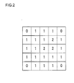
- a clump of defective pixels may be shaped, for example, as shown in Fig. 2 .
- the numerals in this Fig. 2 specify the types of the pixels, with "0" denoting a normal pixel, "1" denoting a defective pixel of the first type, and "2" denoting a defective pixel of the second type.
- the image processing unit 104 performs per se known image processing such as white balance processing, color interpolation processing, edge enhancement processing, side enhancement processing and the like upon the image data that is inputted, and then outputs the image data that has thus been processed to the image recording unit 105.
- This image data is recorded by the image recording unit 105 upon an external storage medium such as, for example, a memory card or the like, or upon an internal storage medium such as a flash memory or the like.
- an external storage medium such as, for example, a memory card or the like
- an internal storage medium such as a flash memory or the like.
- the defective pixel correction unit 103, the image processing unit 104, and the image recording unit 105 are achieved by a CPU and peripheral circuitry.
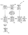
- Fig. 3 is a block diagram showing the structure of the defective pixel correction unit 103.
- the defective pixel correction unit 103 includes a gain correction unit 103a for defective pixels of the first type, a smoothing unit 103b for defective pixels of the first type, an interpolation unit 103c for defective pixels of the second type, a defective pixel position storage memory 103d, and a correction amount storage memory 103e.
- the defective pixel position storage memory 103d and the correction amount storage memory 103e may physically be different areas within the same memory, for example a flash memory, or may be physically different memories.
- An 8 x 8 two dimensional array defect map D(i,j) (where i and j run from 0 to 7) is recorded in the defective pixel position storage memory 103d, as shown in Fig. 4 .
- this defect map D(i,j) normal pixels, defective pixels of the first type, and defective pixels of the second type are distinguished by the code values 0, 1, and 2 respectively.
- the coordinate values (x,y) of the image data in relation to that origin are recorded as the positions of the defective pixels.
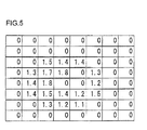
- Correction amounts C(i,j) (where i and j run from 0 to 7) are stored in the correction amount storage memory 103e, for correcting the defective pixels of the first type at the coordinate values (x+i,y+j) in the image data. These correction amounts are the ratio of the output of a normal pixel to the output of the corresponding defective pixel of the first type.
- the positions in the image data of the defective pixels of the first type, the positions of the defective pixels of the second type, and the correction amounts C(i,j) for the defective pixels of the first type are obtained by testing the defective pixel characteristics of the image sensor 102 in the workplace during manufacture of the digital camera 100.
- this testing first, a plurality of sets of image data are acquired while varying the photographic conditions, such as the exposure amount, the color of the incident light, the temperature of the image sensor, the F-value of the lens, the pupil position of the lens, and so on.
- the defective pixels whose outputs are anomalous are detected, and, for each of the defective pixels, the ratio of the output of a normal pixel to the output of that defective pixel is calculated on the basis of these sets of image data.
- correction is performed upon the defective pixel values of the above described plurality of sets of image data by multiplying them by the above ratios. And those defective pixels are classified as being defective pixels of the first type, for which the proportions by which the pixel output values after this correction has been performed differ from the output values for normal pixels are, for example, less than 10%. Moreover, those defective pixels that are not of the first type are classified as being of the second type. And a defect map D(i,j) that is generated on the basis of the results of this classification, and the positions of the defective pixels, are stored in the defective pixel position storage memory 103d. Moreover, correction amounts for the defective pixels of the first type are calculated, and are recorded in the correction amount storage memory 103e.
- an optical image is obtained as image data by exposing the image sensor 102 for a certain time period, and the image data acquired by the image sensor 102 is outputted to the defective pixel correction unit 103.
- the defective pixel correction unit 103 performs processing as described below upon this image data that has been inputted.
- the image data that has been outputted from the image sensor 102 is inputted to the gain correction unit for defective pixels of the first type 103a.
- the gain correction unit for defective pixels of the first type 103a corrects the defective pixel values in the image data by multiplying the pixel values of these defective pixels of the first type (x+i,y+j) that have thus been specified by the correction amounts C (i,j) that are recorded in the correction amount storage memory 103e.
- the smoothing unit for defective pixels of the first type 103b performs smoothing processing upon the values for the defective pixels of the first type that have thus been corrected by the gain correction unit for defective pixels of the first type 103a. By doing this, it is possible to eliminate the gain correction errors due to the gain correction unit for defective pixels of the first type 103a. And, in this smoothing processing, the smoothing unit for defective pixels of the first type 103b smoothes the pixels that are the subj ects of smoothing, in other words the defective pixels of the first type that have been corrected, by referring to pixels, among the pixels that have color filters of the same color as the smoothing subj ect pixels and lie within ranges of 9 x 9 pixels centered upon the smoothing subject pixels, that are not defective.
- the smoothing unit for defective pixels of the first type 103b calculates the average values of those pixel values for which the ratio of the pixel value of the reference subject pixel to the pixel value of the smoothing subject pixel - 1 is within a predetermined value (for example within 12%), and smoothes the pixels that are to be the subjects of smoothing by substituting these average values for their pixel values.
- the pixels that can be referred to during this interpolation processing are all of the pixels within the image, except the defective pixels of the second type.
- the interpolation unit for defective pixels of the second type 103c performs interpolation of the pixel values for the defective pixels of the second type (x+i,y+j), by taking all of the pixels within the image including the defective pixels of the first type that have already been corrected, as being pixels that can be referred to.
- any method for performing interpolation of the pixel values for the defective pixels of the second type (x+i,y+j) will be acceptable, provided that it substitutes, for the pixel values of the pixels that are to be the subj ects of interpolation, the average values of the output values of the neighboring pixels that can be referred to and that have color filters that are the same colors as those of the subject pixels for interpolation, in other words of the defective pixels of the second type (x+i,y+j).
- the defective pixel correction unit 103 After having executed the above described correction processing upon the defective pixels, the defective pixel correction unit 103 outputs the image data after amendment to the image processing unit 104. And, after having performed various types of image processing, as described above, upon the image data that has been inputted, the image processing unit 104 outputs the image data after image processing to the recording unit 105. Then, as described above, the image recording unit 105 records the input data that has thus been inputted upon the storage medium such as a memory card or the like.
Landscapes
- Engineering & Computer Science (AREA)
- Multimedia (AREA)
- Signal Processing (AREA)
- Transforming Light Signals Into Electric Signals (AREA)
- Color Television Image Signal Generators (AREA)
- Image Input (AREA)
Applications Claiming Priority (1)
| Application Number | Priority Date | Filing Date | Title |
|---|---|---|---|
| JP2007339352A JP5141245B2 (ja) | 2007-12-28 | 2007-12-28 | 画像処理装置、補正情報生成方法、および撮像装置 |
Publications (3)
| Publication Number | Publication Date |
|---|---|
| EP2076020A2 true EP2076020A2 (de) | 2009-07-01 |
| EP2076020A3 EP2076020A3 (de) | 2009-08-19 |
| EP2076020B1 EP2076020B1 (de) | 2013-04-17 |
Family
ID=40427454
Family Applications (1)
| Application Number | Title | Priority Date | Filing Date |
|---|---|---|---|
| EP08172896.6A Active EP2076020B1 (de) | 2007-12-28 | 2008-12-24 | Bildverarbeitungsvorrichtung, Erzeugungsverfahren für die Berichtigungsinformation und Bilderfassungsvorrichtung |
Country Status (3)
| Country | Link |
|---|---|
| US (1) | US8149301B2 (de) |
| EP (1) | EP2076020B1 (de) |
| JP (1) | JP5141245B2 (de) |
Cited By (1)
| Publication number | Priority date | Publication date | Assignee | Title |
|---|---|---|---|---|
| EP4654603A1 (de) * | 2024-05-22 | 2025-11-26 | Canon Kabushiki Kaisha | Verarbeitungsvorrichtung, verarbeitungsverfahren und computerprogramm |
Families Citing this family (14)
| Publication number | Priority date | Publication date | Assignee | Title |
|---|---|---|---|---|
| TWI394429B (zh) * | 2009-07-27 | 2013-04-21 | Altek Corp | 消除圖像雜訊之方法,以及使用該方法之裝置 |
| JP5615155B2 (ja) * | 2009-12-22 | 2014-10-29 | キヤノン株式会社 | 画像処理装置及び方法 |
| FR2965441B1 (fr) * | 2010-09-27 | 2013-04-19 | Commissariat Energie Atomique | Procédé de détermination et de correction de la stabilité de réponse d'un détecteur matriciel a semi-conducteur |
| US20120188406A1 (en) * | 2011-01-20 | 2012-07-26 | Apple Inc. | Reduced power consumption filter |
| WO2012150660A1 (ja) * | 2011-05-02 | 2012-11-08 | コニカミノルタアドバンストレイヤー株式会社 | 撮像装置 |
| JP6239820B2 (ja) * | 2011-12-19 | 2017-11-29 | キヤノン株式会社 | 撮像装置及びその制御方法 |
| JP6210266B2 (ja) * | 2013-03-13 | 2017-10-11 | セイコーエプソン株式会社 | カメラ、及び画像処理方法 |
| WO2014156611A1 (ja) * | 2013-03-27 | 2014-10-02 | 株式会社 日立メディコ | 画像処理装置、放射線撮影装置および画像処理方法 |
| DE102013209165A1 (de) | 2013-05-17 | 2014-11-20 | Arnold & Richter Cine Technik Gmbh & Co. Betriebs Kg | Pixelkorrekturverfahren |
| US10666884B1 (en) * | 2019-03-04 | 2020-05-26 | Foveon, Inc. | Method of classifying and correcting image sensor defects utilizing defective-pixel information from color channels |
| DE102019203923B4 (de) * | 2019-03-22 | 2026-05-07 | Carl Zeiss Microscopy Gmbh | Verfahren zur Lokalisierung von Signalquellen in der Lokalisierungsmikroskopie |
| US11494886B2 (en) * | 2020-05-29 | 2022-11-08 | Adobe Inc. | Hierarchical multiclass exposure defects classification in images |
| JP7711703B2 (ja) * | 2020-06-17 | 2025-07-23 | ソニーグループ株式会社 | 画像処理装置、画像処理方法及び画像処理プログラム |
| CN116074495B (zh) * | 2023-03-07 | 2023-06-16 | 合肥埃科光电科技股份有限公司 | 一种图像传感器坏点的检测校正方法及装置 |
Citations (1)
| Publication number | Priority date | Publication date | Assignee | Title |
|---|---|---|---|---|
| JP2005175547A (ja) | 2003-12-05 | 2005-06-30 | Canon Inc | 傷補正回路 |
Family Cites Families (14)
| Publication number | Priority date | Publication date | Assignee | Title |
|---|---|---|---|---|
| US239782A (en) * | 1881-04-05 | Blind-wiring machine | ||
| US165119A (en) * | 1875-06-29 | Improvement in relief-valves | ||
| US222871A (en) * | 1879-12-23 | Improvement in illuminating vault and area covers | ||
| US280721A (en) * | 1883-07-03 | Boiler-feed | ||
| JPH0686104A (ja) * | 1992-09-04 | 1994-03-25 | Matsushita Electric Ind Co Ltd | ノイズリダクション装置 |
| JP3319690B2 (ja) * | 1996-07-03 | 2002-09-03 | 三菱電機株式会社 | 電荷蓄積型受光部を有する撮像装置に用いられるカラー画像信号の処理方法及び処理装置 |
| US20040239782A1 (en) | 2003-05-30 | 2004-12-02 | William Equitz | System and method for efficient improvement of image quality in cameras |
| JP4346968B2 (ja) * | 2003-06-13 | 2009-10-21 | キヤノン株式会社 | 放射線撮影方法、放射線撮影装置、及びコンピュータプログラム |
| JP3952301B2 (ja) | 2003-08-29 | 2007-08-01 | ノーリツ鋼機株式会社 | 画像処理装置、方法、及びプログラム |
| JP4167200B2 (ja) * | 2004-04-13 | 2008-10-15 | 富士フイルム株式会社 | 信号処理装置、信号処理方法及びデジタルカメラ |
| US20050280721A1 (en) * | 2004-06-18 | 2005-12-22 | Van Der Heide Auke | Method for providing combined gain compensation and error correction of a camera pickup array and an apparatus for implementing the method |
| US8009209B2 (en) * | 2005-09-30 | 2011-08-30 | Simon Fraser University | Methods and apparatus for detecting defects in imaging arrays by image analysis |
| JP4754939B2 (ja) | 2005-11-01 | 2011-08-24 | オリンパス株式会社 | 画像処理装置 |
| US8063957B2 (en) | 2006-03-24 | 2011-11-22 | Qualcomm Incorporated | Method and apparatus for processing bad pixels |
-
2007
- 2007-12-28 JP JP2007339352A patent/JP5141245B2/ja not_active Expired - Fee Related
-
2008
- 2008-12-24 EP EP08172896.6A patent/EP2076020B1/de active Active
- 2008-12-24 US US12/318,333 patent/US8149301B2/en active Active
Patent Citations (1)
| Publication number | Priority date | Publication date | Assignee | Title |
|---|---|---|---|---|
| JP2005175547A (ja) | 2003-12-05 | 2005-06-30 | Canon Inc | 傷補正回路 |
Cited By (1)
| Publication number | Priority date | Publication date | Assignee | Title |
|---|---|---|---|---|
| EP4654603A1 (de) * | 2024-05-22 | 2025-11-26 | Canon Kabushiki Kaisha | Verarbeitungsvorrichtung, verarbeitungsverfahren und computerprogramm |
Also Published As
| Publication number | Publication date |
|---|---|
| JP5141245B2 (ja) | 2013-02-13 |
| US8149301B2 (en) | 2012-04-03 |
| EP2076020B1 (de) | 2013-04-17 |
| EP2076020A3 (de) | 2009-08-19 |
| US20090167907A1 (en) | 2009-07-02 |
| JP2009164690A (ja) | 2009-07-23 |
Similar Documents
| Publication | Publication Date | Title |
|---|---|---|
| US8149301B2 (en) | Image processing device, correction information generation method, and image-capturing device | |
| CN111753869B (zh) | 图像处理方法、图像处理装置、存储介质、图像处理系统及已学习模型制造方法 | |
| US8111306B2 (en) | Apparatus, method and computer-readable medium for eliminating dark current components of an image pickup device | |
| JP4700445B2 (ja) | 画像処理装置および画像処理プログラム | |
| US8446477B2 (en) | Imaging apparatus, aberration correcting method, and program | |
| US7405756B2 (en) | Image pickup apparatus | |
| EP1447977A1 (de) | Kompensation von Vignettierung | |
| EP1858252A2 (de) | Verfahren und Vorrichtung zur Bildaufnahme mit der Fähigkeit zur effektiven Wiedergabe von Qualitätsbildern sowie diese verwendende elektronische Vorrichtung | |
| US8482627B2 (en) | Information processing apparatus and method | |
| US10679326B2 (en) | Image data processing apparatus and image data processing method that determine confidence data indicating a level of confidence in a pixel value in high resolution image data | |
| US20090051792A1 (en) | Digital single-lens reflex camera | |
| JPWO2011042948A1 (ja) | 撮像装置の欠陥検出方法及び撮像装置 | |
| WO2011122284A1 (ja) | 画像処理装置、およびそれを用いた撮像装置 | |
| JP5682523B2 (ja) | 画像処理装置、画像処理方法及びプログラム | |
| US20120113301A1 (en) | Image processing apparatus, image capturing apparatus, and image processing method | |
| JP4754939B2 (ja) | 画像処理装置 | |
| JP4513205B2 (ja) | 電子カメラ、および画像処理プログラムの記録媒体 | |
| JP4322921B2 (ja) | カメラモジュールおよびそれを備えた電子機器 | |
| TWI507808B (zh) | 攝影裝置 | |
| CN102202178A (zh) | 图像处理方法及图像处理装置 | |
| US8559762B2 (en) | Image processing method and apparatus for interpolating defective pixels | |
| CN102780888A (zh) | 图像处理装置、图像处理方法以及电子照相机 | |
| JP5309940B2 (ja) | 画像処理装置、および撮像装置 | |
| CN101088284B (zh) | 用于修改图像数据的方法、设备、软件和配置 | |
| JP2009105621A (ja) | プログラム、画像処理装置およびカメラ |
Legal Events
| Date | Code | Title | Description |
|---|---|---|---|
| PUAI | Public reference made under article 153(3) epc to a published international application that has entered the european phase |
Free format text: ORIGINAL CODE: 0009012 |
|
| AK | Designated contracting states |
Kind code of ref document: A2 Designated state(s): AT BE BG CH CY CZ DE DK EE ES FI FR GB GR HR HU IE IS IT LI LT LU LV MC MT NL NO PL PT RO SE SI SK TR |
|
| AX | Request for extension of the european patent |
Extension state: AL BA MK RS |
|
| PUAL | Search report despatched |
Free format text: ORIGINAL CODE: 0009013 |
|
| AK | Designated contracting states |
Kind code of ref document: A3 Designated state(s): AT BE BG CH CY CZ DE DK EE ES FI FR GB GR HR HU IE IS IT LI LT LU LV MC MT NL NO PL PT RO SE SI SK TR |
|
| AX | Request for extension of the european patent |
Extension state: AL BA MK RS |
|
| 17P | Request for examination filed |
Effective date: 20100219 |
|
| AKX | Designation fees paid |
Designated state(s): DE FR GB |
|
| RAP1 | Party data changed (applicant data changed or rights of an application transferred) |
Owner name: NIKON CORPORATION |
|
| 17Q | First examination report despatched |
Effective date: 20100806 |
|
| REG | Reference to a national code |
Ref country code: DE Ref legal event code: R079 Ref document number: 602008023856 Country of ref document: DE Free format text: PREVIOUS MAIN CLASS: H04N0005217000 Ipc: H04N0005367000 |
|
| RIC1 | Information provided on ipc code assigned before grant |
Ipc: H04N 5/367 20110101AFI20120509BHEP |
|
| GRAP | Despatch of communication of intention to grant a patent |
Free format text: ORIGINAL CODE: EPIDOSNIGR1 |
|
| GRAS | Grant fee paid |
Free format text: ORIGINAL CODE: EPIDOSNIGR3 |
|
| GRAA | (expected) grant |
Free format text: ORIGINAL CODE: 0009210 |
|
| AK | Designated contracting states |
Kind code of ref document: B1 Designated state(s): DE FR GB |
|
| REG | Reference to a national code |
Ref country code: GB Ref legal event code: FG4D |
|
| REG | Reference to a national code |
Ref country code: DE Ref legal event code: R096 Ref document number: 602008023856 Country of ref document: DE Effective date: 20130613 |
|
| PLBE | No opposition filed within time limit |
Free format text: ORIGINAL CODE: 0009261 |
|
| STAA | Information on the status of an ep patent application or granted ep patent |
Free format text: STATUS: NO OPPOSITION FILED WITHIN TIME LIMIT |
|
| 26N | No opposition filed |
Effective date: 20140120 |
|
| REG | Reference to a national code |
Ref country code: DE Ref legal event code: R097 Ref document number: 602008023856 Country of ref document: DE Effective date: 20140120 |
|
| REG | Reference to a national code |
Ref country code: FR Ref legal event code: PLFP Year of fee payment: 8 |
|
| REG | Reference to a national code |
Ref country code: FR Ref legal event code: PLFP Year of fee payment: 9 |
|
| REG | Reference to a national code |
Ref country code: FR Ref legal event code: PLFP Year of fee payment: 10 |
|
| REG | Reference to a national code |
Ref country code: DE Ref legal event code: R079 Ref document number: 602008023856 Country of ref document: DE Free format text: PREVIOUS MAIN CLASS: H04N0005367000 Ipc: H04N0025680000 |
|
| P01 | Opt-out of the competence of the unified patent court (upc) registered |
Effective date: 20230517 |
|
| PGFP | Annual fee paid to national office [announced via postgrant information from national office to epo] |
Ref country code: DE Payment date: 20241029 Year of fee payment: 17 |
|
| PGFP | Annual fee paid to national office [announced via postgrant information from national office to epo] |
Ref country code: GB Payment date: 20241104 Year of fee payment: 17 |
|
| PGFP | Annual fee paid to national office [announced via postgrant information from national office to epo] |
Ref country code: FR Payment date: 20241111 Year of fee payment: 17 |