EP2074444B1 - Design of compact adjustable lens - Google Patents
Design of compact adjustable lens Download PDFInfo
- Publication number
- EP2074444B1 EP2074444B1 EP07834763.0A EP07834763A EP2074444B1 EP 2074444 B1 EP2074444 B1 EP 2074444B1 EP 07834763 A EP07834763 A EP 07834763A EP 2074444 B1 EP2074444 B1 EP 2074444B1
- Authority
- EP
- European Patent Office
- Prior art keywords
- adjustable lens
- glass
- lens according
- gel
- elastomer
- Prior art date
- Legal status (The legal status is an assumption and is not a legal conclusion. Google has not performed a legal analysis and makes no representation as to the accuracy of the status listed.)
- Active
Links
Images




Classifications
-
- G—PHYSICS
- G02—OPTICS
- G02B—OPTICAL ELEMENTS, SYSTEMS OR APPARATUS
- G02B26/00—Optical devices or arrangements for the control of light using movable or deformable optical elements
- G02B26/08—Optical devices or arrangements for the control of light using movable or deformable optical elements for controlling the direction of light
- G02B26/0875—Optical devices or arrangements for the control of light using movable or deformable optical elements for controlling the direction of light by means of one or more refracting elements
-
- G—PHYSICS
- G02—OPTICS
- G02B—OPTICAL ELEMENTS, SYSTEMS OR APPARATUS
- G02B27/00—Optical systems or apparatus not provided for by any of the groups G02B1/00 - G02B26/00, G02B30/00
- G02B27/40—Optical focusing aids
-
- G—PHYSICS
- G02—OPTICS
- G02B—OPTICAL ELEMENTS, SYSTEMS OR APPARATUS
- G02B3/00—Simple or compound lenses
- G02B3/12—Fluid-filled or evacuated lenses
- G02B3/14—Fluid-filled or evacuated lenses of variable focal length
-
- G—PHYSICS
- G02—OPTICS
- G02B—OPTICAL ELEMENTS, SYSTEMS OR APPARATUS
- G02B13/00—Optical objectives specially designed for the purposes specified below
- G02B13/001—Miniaturised objectives for electronic devices, e.g. portable telephones, webcams, PDAs, small digital cameras
Definitions
- the present invention is related to design of adjustable lenses, and especially to a design of a lens comprising a gel or elastomer disposed on bendable glass, wherein a piezo electric element is arranged in contact with the glass providing a bending of the glass when voltage is applied on the piezo electric element providing adjustment of lens parameters.
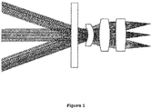
- FIG. 1 A schematic illustration of a lens stack is illustrated in Figure 1 .
- the focus lens rectangular in the schematic
- the role of the focus lens element is to shift focal point continuously from infinity to a minimum focal distance, which is determined by the application of the camera, for example.
- Focal distances may be in the range of 5-50 cm, for example.
- JP 02-178602 disclose a lens assembly wherein a couple of transparent base materials with a liquid in between provides a bending of the base materials by applying a voltage on piezo electric elements disposed on one of the base materials, wherein the bending provides a desired curvature of the surfaces of the lens assembly.
- JP 2000-249813 discloses a lens assembly comprising a deformable transparent material disposed in between two bendable transparent plates.
- a common actuator can bend the plates to provide a shift of the focal length of the lens assembly.
- JP 01-140118 discloses an adjustable lens assembly comprising a piezo electric polymer with transparent electrodes on top of a cylinder container comprising a transparent liquid. Voltages applied onto the piezo electric polymer provides a curvature of the polymer, and hence a shift of focal length. Further prior art US 6 188 526 B1 discloses an adjustable lens comprising a cover member hold on a liquid and actuated by a piezoelectric actuator.
- a lens assembly comprising at least one support 14 supporting a gel or elastomer 13 comprising a thin glass cover 11, wherein a circular shaped middle part 18 of the thin glass cover is arranged as an island 18 with no contact to the rest of the glass cover 11, floating on top of the gel 13, wherein a thin circular piezo electric ring shaped crystal 12 is disposed in contact with the edge of the glass island 18, the rest of the glass cover 11 is disposed on top of the gel 13 until the edges of the at least one support 14, wherein spacer elements 14 along the edge of the at least one support 14 provides electric connections 16 for signals applied on the piezoelectric ring 12, and wherein the spacer elements 14 at the same time provides mechanical support and fixation of the glass cover 11 to the at least one support 14.
- via holes in electric contact with the spacer elements 14 provides pads for connecting the lens assembly electrically to the top of a camera assembly.
- a design of an adjustable optical lens provides a lens wherein the total size of the lens including electrical contacting is small enough to be implemented in a stack of other optical elements, and is not exceeding the size of the other elements in the stack.
- spacer members 14 also acts as a spacer element 14 during manufacturing of the lens.
- Digital camera modules comprises, for example:
- any tuneable functionality in an optical system must per se include some adjustable lens element or parameter.
- Focal properties can be adjusted for example by physically moving lenses relative to each other, or by deforming the physical shape of a lens. It will be obvious that an adjustable lens element that contains no moving parts will have the potential of being both more reliable and more cost efficient during manufacturing.
- deformable lenses has been a topic of high interest. And with the introduction of digital camera solutions into high volume consumer products, such as compact cameras, mobile phones and PCs, the demand for higher quality, lower cost camera module systems has increased. Adding features like zoom and auto focus functionalities will give added value to the camera solutions in such applications.
- tuneable parameters may be of interest when the lens system is used in a light measuring device or instrument based on light properties.
- Any adjustable lens parameter related to the application of the lens assembly according to the present invention is regarded as being inside the scope of the present invention.
- wafer production is one of the most effective manners to achieve mass production of micro electronics and micromechanical components.
- adjustable lens elements it is highly desirable also to implement adjustable lenses in a stack with other lenses and/or other optical elements, such as optical sensors etc. on a wafer scale production. This can be feasible if the lateral size of the lens element do not exceed the size of the other elements in the wafer stack. None of the prior art techniques can combine low cost with the possibility to implement adjustable lenses on a wafer scale manufacturing of for example compact digital camera modules for implementation into mobile phones, cameras, pc's etc.
- the bottom substrate 10 is a support element, made of any transparent, relatively rigid material, such as any glass or transparent polymeric material.
- the top element 11 is another relatively rigid material, including an actuating element, such as a piezoelectric element 12. Sandwiched between these is a deformable, transparent material, such as a polymer gel or elastomer 13, or a branched or linear polymer or oily liquid.
- the basic principle of the actuation that defines the adjustable lens is the direct deformation of the actuator/cover material that creates a curvature.
- the curvature radius defines the focusing properties of the lens, as known to a person skilled in the art.
- the present invention is relates to the above disclosed design, wherein the total lens assembly also includes at least one support element that act as spacers during manufacture, in order to provide the necessary thickness of the sandwiched flexible material, and as a stabilizing element, that provides increased mechanical stability of the whole adjustable lens assembly.
- the functionality of the adjustable lens lies in the disk 18 that is bendable.
- the bendable disk 18 therefore has to be relatively unattached; it must be floating atop the deformable (polymer) material 13.
- the flexible material 13 (the polymer) has uniform thickness over the entire lens element as illustrated in Figure 2 , 3 and 4 , for example.
- the flexible material 13 is shaped such that it has a lower thickness in the area between the actuator element 12 and the stabilizing elements 14 as depicted in figure 5 .
- the flexible material 13 is removed from parts of the area between the actuator element 12and the stabilizing elements 14.
- An important aspect of the present invention is to have support/spacing elements 14 that are electrically conductive. This facilitates an effective routing of electrical signals, and in contacting the actuator element to an external voltage supply and control unit.
- An optical system for a camera, mobile phone or laptop contains a lens stack with variable focus capability, a sensor array and electronics for amplification, conditioning and conversion of the optical signals.
- the interface to the focus part of the optical system is through the I/O device of the electronics.
- the electrical interface consists of two connectors supplying the control signal from the auto focus device of the electronics. If an adjustable lens element in a cost effective way shall be included on a wafer level assembly of a camera module, the introduction of it must not lead to an increase in the total lateral size of the camera module; thus, the location of the signal connectors from the auto focus algorithm is geometrically confined to within the total lateral dimensions of the image sensor.
- the transparent support 10 is provided by glass on silicon, wherein an opening is arranged in the silicon to allow light to pass the lens assembly.
- electronics for driving the piezo electric element 12 or a plurality of piezo electric elements, and control logic is integrated in the silicon part of the transparent assembly, or as a hybrid circuit bonded to the support 10. The signals are connected to the conductors 16 in the spacer elements 14.
- through-holes in the cover glass is provided, or alternatively, removing of the cover glass above the support elements 14.
- Through holes can also be included in the bottom support substrate 10, as illustrated in Fig 6 .
- electrical contacts to the actuator 12 on the glass island top 18 is provided by for example metal bonding on the bottom side of the lens element, which facilitates the implementation of the lens element in extremely compact optical stacks.
- the spacer members 14 are embodied as a mechanically stable structures along the edges of the adjustable lens element, as a wall, that facilitates the possible horizontal inversion of the lens element, in other words having the deformable surface of the focus lens closest to the image sensor. This has the advantage of making electrical contact to the (piezo electrical) actuator 12 easier to accomplish.
- Another example of embodiment of the invention is thus to invert the adjustable lens element, so that the side of the lens element on which the actuator is located is directly connected to the rest of the lens stack below it, as illustrated in Figure 8 .
- a protecting and mechanically stabilizing cover element (cover glass) 17 that encapsulates the whole lens element is disposed as illustrated in figure 7 .
- the piezo electric element 12 bending the glass island 18 is arranged as a plurality of independent actuator elements 12 providing a possibility to achieve an asymmetric lens configuration by applying different voltages on the plurality of individual piezo electric elements, for example changing the line of sight without actually moving the lens assembly.
- the shape of the glass island 18 comprising the piezo electric element can have any shape, not only circular, but any shape adapted to the use of the adjustable lens, for example for instrumentation purposes.
- a specific shape of the glass island By providing a specific shape of the glass island, a specific compression of the gel or elastomer 13 is achievable, thereby providing a means of controlling lens parameters through the shaping of the deformations, as known to a person skilled in the art.
- the piezo electric element 12 can be provided as one piece of element arranged in contact with the glass island 18 on either side of the glass island 18, and in any pattern or shape of the piezo electric element 12. Such arrangement will provide different bending properties of the glass island, and hence different shaping of the deformation of the gel or elastomer, and hence change in optical parameters.
Landscapes
- Physics & Mathematics (AREA)
- General Physics & Mathematics (AREA)
- Optics & Photonics (AREA)
- Lens Barrels (AREA)
- Lenses (AREA)
- Studio Devices (AREA)
- Liquid Crystal (AREA)
Description
- The present invention is related to design of adjustable lenses, and especially to a design of a lens comprising a gel or elastomer disposed on bendable glass, wherein a piezo electric element is arranged in contact with the glass providing a bending of the glass when voltage is applied on the piezo electric element providing adjustment of lens parameters.
- There is an increasing demand for low cost, high volume solutions for adjustable lens elements in an ever increasing number of applications. The popular use of cameras in mobile phones represents an amount of millions of lenses. The design of such lenses requires fulfilment of a plurality of requirements, such as ease of operation when fitting the lens on top of a camera module in the mobile phone, providing as few operational steps as possible, etc. These challenges are even greater when the lens arrangement comprises tuneable parameters, such as encountered in auto focus lenses, wherein the focal length must be adjusted to fit the distance from the lens to the object to be photographed, for example. Such lenses are usually complex designs comprising movable parts, for example, which can make it difficult to assemble the lens in a reasonable manner. A further challenge with such designs are the ever increasing requirement to provide as thin lens assemblies as possible. Thin and lightweight mobile phones and cameras is a must in the marketplace.
- Usually, it is necessary to have a stack of lenses atop an image sensor (a CMOS or CCD sensor), in order to focus light from the object to be photographed down to the sensor. A schematic illustration of a lens stack is illustrated in
Figure 1 . By proper design of the total lens stack, the focus lens (rectangular in the schematic) can be located either closest to the photographing object or in between other lens elements. The role of the focus lens element is to shift focal point continuously from infinity to a minimum focal distance, which is determined by the application of the camera, for example. Focal distances may be in the range of 5-50 cm, for example. - In prior art there are some examples of compact adjustable lens designs. For example, in the article "Design, fabrication and testing of a micro machines integrated tuneable micro lens", by Weisong et. A1., Journal of Micromechanics and Microengineering, 9 May, 2006, disclose a lens assembly wherein a liquid in a cavity may be compressed or elongated to achieve an adjustment of focal length of the lens. However, mass production comprising filling liquid may be a difficult and time consuming task.
-
JP 02-178602 -
JP 2000-249813 -
JP 01-140118 US 6 188 526 B1 discloses an adjustable lens comprising a cover member hold on a liquid and actuated by a piezoelectric actuator. - Therefore there is a need for a lens design providing simple adjustment of the lens, wherein the lens assembly is easy and cheap to mass produce.
- According to an aspect of the present invention, a lens assembly comprising at least one
support 14 supporting a gel orelastomer 13 comprising athin glass cover 11, wherein a circular shapedmiddle part 18 of the thin glass cover is arranged as anisland 18 with no contact to the rest of theglass cover 11, floating on top of thegel 13, wherein a thin circular piezo electric ring shapedcrystal 12 is disposed in contact with the edge of theglass island 18, the rest of theglass cover 11 is disposed on top of thegel 13 until the edges of the at least onesupport 14, whereinspacer elements 14 along the edge of the at least onesupport 14 provideselectric connections 16 for signals applied on thepiezoelectric ring 12, and wherein thespacer elements 14 at the same time provides mechanical support and fixation of theglass cover 11 to the at least onesupport 14. - In an example of embodiment of the present invention, via holes in electric contact with the
spacer elements 14 provides pads for connecting the lens assembly electrically to the top of a camera assembly. - According to another example of embodiment of the present invention, a design of an adjustable optical lens provides a lens wherein the total size of the lens including electrical contacting is small enough to be implemented in a stack of other optical elements, and is not exceeding the size of the other elements in the stack.
- According to another example of embodiment of the
invention spacer members 14 also acts as aspacer element 14 during manufacturing of the lens. -
-
Figure 1 illustrates schematically the principle of a stack of lenses in a camera module. -
Figure 2 depicts the design principle of a lens assembly according to the present invention. -
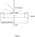
Figure 3 depicts another view of the design principle of a lens assembly according to the present invention. -
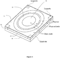
Figure 4 depicts a perspective view of the lens design illustrated infigure 2 and3 . -
Figure 5 illustrates another example of embodiment of the present invention. -
Figure 6 illustrates yet another example of embodiment of the present invention. -
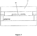
Figure 7 illustrates disposal of protective cover. -
Figure 8 illustrates an example of embodiment, in which the adjustable lens element is inverted horizontally. - Digital camera modules comprises, for example:
- an image sensor (CCD or CMOS sensor)
- colour filters, with micro lens arrays
- lens stack for focusing light from photographing object down to the sensor
- if auto focus or zoom functionality is to be included, a tuneable lens element must be included somewhere in the lens system
- Any tuneable functionality in an optical system (auto focus, zoom) must per se include some adjustable lens element or parameter. Focal properties can be adjusted for example by physically moving lenses relative to each other, or by deforming the physical shape of a lens. It will be obvious that an adjustable lens element that contains no moving parts will have the potential of being both more reliable and more cost efficient during manufacturing. The development of deformable lenses has been a topic of high interest. And with the introduction of digital camera solutions into high volume consumer products, such as compact cameras, mobile phones and PCs, the demand for higher quality, lower cost camera module systems has increased. Adding features like zoom and auto focus functionalities will give added value to the camera solutions in such applications.
- According to another aspect of the present invention, other tuneable parameters may be of interest when the lens system is used in a light measuring device or instrument based on light properties. Any adjustable lens parameter related to the application of the lens assembly according to the present invention, is regarded as being inside the scope of the present invention.
- As known to a person skilled in the art, wafer production is one of the most effective manners to achieve mass production of micro electronics and micromechanical components. One of the challenges that arises when compactness and low cost is requirements, it is necessary to implement wafer scale processing throughout the whole production cycle. For certain applications of adjustable lens elements, it is highly desirable also to implement adjustable lenses in a stack with other lenses and/or other optical elements, such as optical sensors etc. on a wafer scale production. This can be feasible if the lateral size of the lens element do not exceed the size of the other elements in the wafer stack. None of the prior art techniques can combine low cost with the possibility to implement adjustable lenses on a wafer scale manufacturing of for example compact digital camera modules for implementation into mobile phones, cameras, pc's etc.
- There exist a number of technologically feasible solutions for making compact adjustable lenses, for use in applications such as (auto) focus lenses or zoom lenses. This invention relates to a design of an adjustable lens that consists of a stack of materials as depicted in
Figure 2 ,3 and4 . Thebottom substrate 10 is a support element, made of any transparent, relatively rigid material, such as any glass or transparent polymeric material. Thetop element 11 is another relatively rigid material, including an actuating element, such as apiezoelectric element 12. Sandwiched between these is a deformable, transparent material, such as a polymer gel orelastomer 13, or a branched or linear polymer or oily liquid. The basic principle of the actuation that defines the adjustable lens is the direct deformation of the actuator/cover material that creates a curvature. The curvature radius defines the focusing properties of the lens, as known to a person skilled in the art. - The present invention is relates to the above disclosed design, wherein the total lens assembly also includes at least one support element that act as spacers during manufacture, in order to provide the necessary thickness of the sandwiched flexible material, and as a stabilizing element, that provides increased mechanical stability of the whole adjustable lens assembly.
- The functionality of the adjustable lens lies in the
disk 18 that is bendable. Thebendable disk 18 therefore has to be relatively unattached; it must be floating atop the deformable (polymer)material 13. By introducing the stabilizingsupport elements 14, as depicted inFigures 2 and3 , the following advantages are evident: - The stabilizing
elements 14 give increased mechanical stability of the whole lens assembly, which is important both for the handling of wafers during manufacturing and assembly with other wafers (for example lens stacks and image sensors) and during singulation (sawing) of the wafer stack into individual camera modules, and during further integration of the camera modules into their intended application (mobile phones, digital cameras, PC cameras etc.) - The stabilizing elements act as
spacers 14 during manufacturing of the adjustable lens element, which is necessary for the application of for example a defined amount/thickness of a liquid pre-polymer. - In an example of embodiment of the present invention, the flexible material 13 (the polymer) has uniform thickness over the entire lens element as illustrated in
Figure 2 ,3 and4 , for example. - In another example of embodiment of the present invention, the
flexible material 13 is shaped such that it has a lower thickness in the area between theactuator element 12 and the stabilizingelements 14 as depicted infigure 5 . - In yet another example of embodiment of the present invention, the
flexible material 13 is removed from parts of the area between the actuator element 12and the stabilizingelements 14. - An important aspect of the present invention is to have support/
spacing elements 14 that are electrically conductive. This facilitates an effective routing of electrical signals, and in contacting the actuator element to an external voltage supply and control unit. - An optical system for a camera, mobile phone or laptop contains a lens stack with variable focus capability, a sensor array and electronics for amplification, conditioning and conversion of the optical signals. The interface to the focus part of the optical system is through the I/O device of the electronics. The electrical interface consists of two connectors supplying the control signal from the auto focus device of the electronics. If an adjustable lens element in a cost effective way shall be included on a wafer level assembly of a camera module, the introduction of it must not lead to an increase in the total lateral size of the camera module; thus, the location of the signal connectors from the auto focus algorithm is geometrically confined to within the total lateral dimensions of the image sensor.
- According to another example of embodiment of the present invention, the
transparent support 10 is provided by glass on silicon, wherein an opening is arranged in the silicon to allow light to pass the lens assembly. In an example of embodiment of the present invention, electronics for driving the piezoelectric element 12 or a plurality of piezo electric elements, and control logic is integrated in the silicon part of the transparent assembly, or as a hybrid circuit bonded to thesupport 10. The signals are connected to theconductors 16 in thespacer elements 14. - In an example of embodiment of the present invention, through-holes in the cover glass is provided, or alternatively, removing of the cover glass above the
support elements 14. Through holes can also be included in thebottom support substrate 10, as illustrated inFig 6 . The key aspect of this embodiment is that electrical contacts to theactuator 12 on theglass island top 18 is provided by for example metal bonding on the bottom side of the lens element, which facilitates the implementation of the lens element in extremely compact optical stacks. - According to another example of embodiment of the present invention, the
spacer members 14 are embodied as a mechanically stable structures along the edges of the adjustable lens element, as a wall, that facilitates the possible horizontal inversion of the lens element, in other words having the deformable surface of the focus lens closest to the image sensor. This has the advantage of making electrical contact to the (piezo electrical)actuator 12 easier to accomplish. - Another example of embodiment of the invention is thus to invert the adjustable lens element, so that the side of the lens element on which the actuator is located is directly connected to the rest of the lens stack below it, as illustrated in
Figure 8 . - According to yet another example of embodiment of the present invention, a protecting and mechanically stabilizing cover element (cover glass) 17 that encapsulates the whole lens element is disposed as illustrated in
figure 7 . - According to yet another example of embodiment of the present invention, the piezo
electric element 12 bending theglass island 18 is arranged as a plurality ofindependent actuator elements 12 providing a possibility to achieve an asymmetric lens configuration by applying different voltages on the plurality of individual piezo electric elements, for example changing the line of sight without actually moving the lens assembly. - According to yet another example of embodiment of the present invention, the shape of the
glass island 18 comprising the piezo electric element can have any shape, not only circular, but any shape adapted to the use of the adjustable lens, for example for instrumentation purposes. By providing a specific shape of the glass island, a specific compression of the gel orelastomer 13 is achievable, thereby providing a means of controlling lens parameters through the shaping of the deformations, as known to a person skilled in the art. - Further, the piezo
electric element 12 can be provided as one piece of element arranged in contact with theglass island 18 on either side of theglass island 18, and in any pattern or shape of the piezoelectric element 12. Such arrangement will provide different bending properties of the glass island, and hence different shaping of the deformation of the gel or elastomer, and hence change in optical parameters.
Claims (15)
- Adjustable lens comprising:a transparent support substrate (10) with a disposed gel or elastomer (13) on a side of the support (10), wherein a thin glass cover (11) is disposed on top of the gel or elastomer (13), wherein the thin glass cover (11) is arranged with a circular shaped glass cut-out (18) in the middle defining a glass island (18) without any mechanical contact with the rest of the thin glass cover (11), wherein at least one piezo electric element (12) is in contact with edges of the glass island (18), wherein at least one spacer member (14) is arranged along one edge of the transparent support (10), wherein the at least one spacer member (14) is supporting the thin glass cover (11), wherein the at least one spacer element comprises electric conducting materials providing electric contacting of the adjustable lens with other components of an optical system and wherein spacer elements (14) along the edge of the at least one support provides electric connections (16) for signals applied on the piezoelectric ring element (12).
- The adjustable lens according to claim 1, wherein the transparent support (10) is provided by glass on silicon substrate, wherein an opening is arranged in the silicon substrate letting light pass through the adjustable lens.
- The adjustable lens according to claim 2, wherein the silicon substrate comprise electronic components related to the at least one piezo electric element (12).
- The adjustable lens according to claim 3, wherein the electronic components are provided as separate circuits supported by the silicon substrate of the transparent support (10).
- The adjustable lens according to claim 1, wherein the gel or elastomer (13) has uniform thickness throughout the entire adjustable lens.
- The adjustable lens according to claim 1, wherein the gel or elastomer (13) has a less thickness in the area between the at least one piezo electric element (12) and the at least one spacer member (14) compared to the thickness of the rest of the gel or elastomer (13).
- The adjustable lens according to claim 1, wherein an additional protective glass (17) is arranged partly around the adjustable lens.
- The adjustable lens according to claim 1, wherein the at least one spacer member (14) is arranged as a wall around the perimeter of the adjustable lens.
- The adjustable lens according to claim 1, wherein an image sensor is arranged as an integral part of the adjustable lens by arranging the at least one spacer member (14) to support components of the adjustable lens such that the gel or elastomer (13) is disposed on the one side of the transparent support (10) with the glass island (18) floating on top of the gel or elastomer (13), wherein the at least one spacer member (14) provides a space in the lens assembly for attaching the image sensor on to the at least one spacer member (14) at an end of the at least one spacer member (14) opposite the side of the transparent support (10).
- The adjustable lens according to claim 9, wherein a fixed micro lens (19) is arranged in the space provided by the at least one spacer member (14) for attaching the image sensor.
- The adjustable lens according to claim 1, wherein the at least one piezo electric element (12) is arranged as a plurality of independent piezo electric elements (12) along edges of the glass island (18).
- Method of use of the adjustable lens according to claim 1, wherein the glass cut-out (18) has a shape adapted to the use of the adjustable lens.
- The adjustable lens according to claim 1, wherein the at least one piezo electric element (12) is disposed on top of the glass island (18) on the side facing away from the gel or elastomer (13) along the edges of the glass island (18).
- The adjustable lens according to claim 1, wherein the at least one piezo electric element (12) is disposed on the bottom side of the glass island (18) facing towards the gel or elastomer (13) along the edges of the glass island (18).
- Method of use of the adjustable lens according to claim 1, wherein the at least one piezo electric element (12) is disposed in contact with the glass island (18) in a pattern that is adapted to the use of the adjustable lens.
Applications Claiming Priority (3)
| Application Number | Priority Date | Filing Date | Title |
|---|---|---|---|
| NO20064625 | 2006-10-11 | ||
| NO20065237 | 2006-11-14 | ||
| PCT/NO2007/000350 WO2008044937A1 (en) | 2006-10-11 | 2007-10-05 | Design of compact adjustable lens |
Publications (3)
| Publication Number | Publication Date |
|---|---|
| EP2074444A1 EP2074444A1 (en) | 2009-07-01 |
| EP2074444A4 EP2074444A4 (en) | 2011-12-21 |
| EP2074444B1 true EP2074444B1 (en) | 2017-08-30 |
Family
ID=39283072
Family Applications (1)
| Application Number | Title | Priority Date | Filing Date |
|---|---|---|---|
| EP07834763.0A Active EP2074444B1 (en) | 2006-10-11 | 2007-10-05 | Design of compact adjustable lens |
Country Status (6)
| Country | Link |
|---|---|
| US (1) | US8045280B2 (en) |
| EP (1) | EP2074444B1 (en) |
| JP (1) | JP5244806B2 (en) |
| KR (1) | KR101360455B1 (en) |
| CN (1) | CN101600976B (en) |
| WO (1) | WO2008044937A1 (en) |
Cited By (1)
| Publication number | Priority date | Publication date | Assignee | Title |
|---|---|---|---|---|
| EP4130643A3 (en) * | 2021-08-01 | 2023-03-01 | Bird Aerosystems Ltd. | Device, system, and method of aircraft protection and countermeasures against missiles |
Families Citing this family (83)
| Publication number | Priority date | Publication date | Assignee | Title |
|---|---|---|---|---|
| NO326372B1 (en) * | 2006-09-21 | 2008-11-17 | Polight As | Polymer Lens |
| KR101360545B1 (en) * | 2006-10-11 | 2014-02-10 | 포라이트 에이에스 | Method for manufacturing adjustable lens |
| US8390939B2 (en) | 2007-02-12 | 2013-03-05 | Polight As | Flexible lens assembly with variable focal length |
| JP2011523538A (en) | 2008-05-20 | 2011-08-11 | ペリカン イメージング コーポレイション | Image capture and processing using monolithic camera arrays with different types of imagers |
| US11792538B2 (en) | 2008-05-20 | 2023-10-17 | Adeia Imaging Llc | Capturing and processing of images including occlusions focused on an image sensor by a lens stack array |
| US8866920B2 (en) | 2008-05-20 | 2014-10-21 | Pelican Imaging Corporation | Capturing and processing of images using monolithic camera array with heterogeneous imagers |
| CN106324728B (en) * | 2008-07-11 | 2018-09-04 | 珀莱特公司 | Method and apparatus for reducing the fuel factor in compact adjustable optical lens |
| WO2010015093A1 (en) | 2008-08-08 | 2010-02-11 | Optotune Ag | Electroactive optical device |
| WO2011063347A2 (en) | 2009-11-20 | 2011-05-26 | Pelican Imaging Corporation | Capturing and processing of images using monolithic camera array with heterogeneous imagers |
| JP5430413B2 (en) * | 2010-01-07 | 2014-02-26 | 富士フイルム株式会社 | Variable focus lens and driving method thereof |
| WO2011143501A1 (en) | 2010-05-12 | 2011-11-17 | Pelican Imaging Corporation | Architectures for imager arrays and array cameras |
| US8878950B2 (en) | 2010-12-14 | 2014-11-04 | Pelican Imaging Corporation | Systems and methods for synthesizing high resolution images using super-resolution processes |
| US8559806B2 (en) * | 2010-12-29 | 2013-10-15 | Samsung Electro-Mechanics Co., Ltd. | Camera module and method for manufacturing the same |
| EP2708019B1 (en) | 2011-05-11 | 2019-10-16 | FotoNation Limited | Systems and methods for transmitting and receiving array camera image data |
| US20130265459A1 (en) | 2011-06-28 | 2013-10-10 | Pelican Imaging Corporation | Optical arrangements for use with an array camera |
| JP2014521117A (en) | 2011-06-28 | 2014-08-25 | ペリカン イメージング コーポレイション | Optical array for use with array cameras |
| WO2013043761A1 (en) | 2011-09-19 | 2013-03-28 | Pelican Imaging Corporation | Determining depth from multiple views of a scene that include aliasing using hypothesized fusion |
| US9129183B2 (en) | 2011-09-28 | 2015-09-08 | Pelican Imaging Corporation | Systems and methods for encoding light field image files |
| US20130088637A1 (en) * | 2011-10-11 | 2013-04-11 | Pelican Imaging Corporation | Lens Stack Arrays Including Adaptive Optical Elements |
| US9412206B2 (en) | 2012-02-21 | 2016-08-09 | Pelican Imaging Corporation | Systems and methods for the manipulation of captured light field image data |
| US9210392B2 (en) | 2012-05-01 | 2015-12-08 | Pelican Imaging Coporation | Camera modules patterned with pi filter groups |
| KR102077853B1 (en) * | 2012-06-01 | 2020-02-14 | 엘지이노텍 주식회사 | AF apparatus for Camera Module |
| EP2873028A4 (en) | 2012-06-28 | 2016-05-25 | Pelican Imaging Corp | SYSTEMS AND METHODS FOR DETECTING CAMERA NETWORKS, OPTICAL NETWORKS AND DEFECTIVE SENSORS |
| US20140002674A1 (en) | 2012-06-30 | 2014-01-02 | Pelican Imaging Corporation | Systems and Methods for Manufacturing Camera Modules Using Active Alignment of Lens Stack Arrays and Sensors |
| TWI527182B (en) * | 2012-08-09 | 2016-03-21 | 台灣愛美科股份有限公司 | Telescopic unit and retractable mesh structure with retractable unit |
| KR102111181B1 (en) | 2012-08-21 | 2020-05-15 | 포토내이션 리미티드 | Systems and methods for parallax detection and correction in images captured using array cameras |
| WO2014032020A2 (en) | 2012-08-23 | 2014-02-27 | Pelican Imaging Corporation | Feature based high resolution motion estimation from low resolution images captured using an array source |
| CN102879900A (en) * | 2012-09-11 | 2013-01-16 | 电子科技大学 | Zoom micro lens based on piezoelectric inverse effect |
| WO2014043641A1 (en) | 2012-09-14 | 2014-03-20 | Pelican Imaging Corporation | Systems and methods for correcting user identified artifacts in light field images |
| EP2901671A4 (en) | 2012-09-28 | 2016-08-24 | Pelican Imaging Corp | CREATING IMAGES FROM LIGHT FIELDS USING VIRTUAL POINTS OF VIEW |
| US9595553B2 (en) | 2012-11-02 | 2017-03-14 | Heptagon Micro Optics Pte. Ltd. | Optical modules including focal length adjustment and fabrication of the optical modules |
| WO2014078443A1 (en) | 2012-11-13 | 2014-05-22 | Pelican Imaging Corporation | Systems and methods for array camera focal plane control |
| US9462164B2 (en) | 2013-02-21 | 2016-10-04 | Pelican Imaging Corporation | Systems and methods for generating compressed light field representation data using captured light fields, array geometry, and parallax information |
| WO2014133974A1 (en) | 2013-02-24 | 2014-09-04 | Pelican Imaging Corporation | Thin form computational and modular array cameras |
| WO2014138697A1 (en) | 2013-03-08 | 2014-09-12 | Pelican Imaging Corporation | Systems and methods for high dynamic range imaging using array cameras |
| US8866912B2 (en) | 2013-03-10 | 2014-10-21 | Pelican Imaging Corporation | System and methods for calibration of an array camera using a single captured image |
| WO2014165244A1 (en) | 2013-03-13 | 2014-10-09 | Pelican Imaging Corporation | Systems and methods for synthesizing images from image data captured by an array camera using restricted depth of field depth maps in which depth estimation precision varies |
| US9106784B2 (en) | 2013-03-13 | 2015-08-11 | Pelican Imaging Corporation | Systems and methods for controlling aliasing in images captured by an array camera for use in super-resolution processing |
| WO2014164909A1 (en) | 2013-03-13 | 2014-10-09 | Pelican Imaging Corporation | Array camera architecture implementing quantum film sensors |
| US9124831B2 (en) | 2013-03-13 | 2015-09-01 | Pelican Imaging Corporation | System and methods for calibration of an array camera |
| US9100586B2 (en) | 2013-03-14 | 2015-08-04 | Pelican Imaging Corporation | Systems and methods for photometric normalization in array cameras |
| US9578259B2 (en) | 2013-03-14 | 2017-02-21 | Fotonation Cayman Limited | Systems and methods for reducing motion blur in images or video in ultra low light with array cameras |
| US9497429B2 (en) | 2013-03-15 | 2016-11-15 | Pelican Imaging Corporation | Extended color processing on pelican array cameras |
| US9445003B1 (en) | 2013-03-15 | 2016-09-13 | Pelican Imaging Corporation | Systems and methods for synthesizing high resolution images using image deconvolution based on motion and depth information |
| JP2016524125A (en) | 2013-03-15 | 2016-08-12 | ペリカン イメージング コーポレイション | System and method for stereoscopic imaging using a camera array |
| US9633442B2 (en) | 2013-03-15 | 2017-04-25 | Fotonation Cayman Limited | Array cameras including an array camera module augmented with a separate camera |
| US10122993B2 (en) | 2013-03-15 | 2018-11-06 | Fotonation Limited | Autofocus system for a conventional camera that uses depth information from an array camera |
| WO2014150856A1 (en) | 2013-03-15 | 2014-09-25 | Pelican Imaging Corporation | Array camera implementing quantum dot color filters |
| EP2781939B1 (en) | 2013-03-18 | 2015-11-04 | poLight AS | Deformable polymeric lens |
| WO2015048694A2 (en) | 2013-09-27 | 2015-04-02 | Pelican Imaging Corporation | Systems and methods for depth-assisted perspective distortion correction |
| US9426343B2 (en) | 2013-11-07 | 2016-08-23 | Pelican Imaging Corporation | Array cameras incorporating independently aligned lens stacks |
| US10119808B2 (en) | 2013-11-18 | 2018-11-06 | Fotonation Limited | Systems and methods for estimating depth from projected texture using camera arrays |
| WO2015081279A1 (en) | 2013-11-26 | 2015-06-04 | Pelican Imaging Corporation | Array camera configurations incorporating multiple constituent array cameras |
| KR102184042B1 (en) * | 2014-01-29 | 2020-11-27 | 엘지이노텍 주식회사 | Camera apparatus |
| US10089740B2 (en) | 2014-03-07 | 2018-10-02 | Fotonation Limited | System and methods for depth regularization and semiautomatic interactive matting using RGB-D images |
| US9247117B2 (en) | 2014-04-07 | 2016-01-26 | Pelican Imaging Corporation | Systems and methods for correcting for warpage of a sensor array in an array camera module by introducing warpage into a focal plane of a lens stack array |
| US9224022B2 (en) | 2014-04-29 | 2015-12-29 | Hand Held Products, Inc. | Autofocus lens system for indicia readers |
| US9521319B2 (en) | 2014-06-18 | 2016-12-13 | Pelican Imaging Corporation | Array cameras and array camera modules including spectral filters disposed outside of a constituent image sensor |
| EP3467776A1 (en) | 2014-09-29 | 2019-04-10 | Fotonation Cayman Limited | Systems and methods for dynamic calibration of array cameras |
| US9942474B2 (en) | 2015-04-17 | 2018-04-10 | Fotonation Cayman Limited | Systems and methods for performing high speed video capture and depth estimation using array cameras |
| TWI622294B (en) * | 2016-06-15 | 2018-04-21 | 聚晶半導體股份有限公司 | Imgae pickup module and the manufacutring method thereof |
| WO2019002448A1 (en) * | 2017-06-30 | 2019-01-03 | Polight As | ADAPTIVE LENS |
| CN107450148A (en) * | 2017-08-03 | 2017-12-08 | 江西合力泰科技有限公司 | Optical anti-vibration camera module and its control method |
| US10482618B2 (en) | 2017-08-21 | 2019-11-19 | Fotonation Limited | Systems and methods for hybrid depth regularization |
| CN109167909B (en) | 2018-11-26 | 2020-07-24 | Oppo广东移动通信有限公司 | Imaging modules and electronic devices |
| IT201900005802A1 (en) * | 2019-04-15 | 2020-10-15 | St Microelectronics Srl | MEMS OPTICAL DEVICE INCLUDING A LENS AND AN ACTUATOR TO CHECK THE CURVATURE OF THE LENS, AND RELATED MANUFACTURING PROCEDURE |
| KR102646521B1 (en) | 2019-09-17 | 2024-03-21 | 인트린식 이노베이션 엘엘씨 | Surface modeling system and method using polarization cue |
| MX2022004163A (en) | 2019-10-07 | 2022-07-19 | Boston Polarimetrics Inc | SYSTEMS AND METHODS FOR THE DETECTION OF SURFACE STANDARDS WITH POLARIZATION. |
| CN110764262A (en) * | 2019-10-08 | 2020-02-07 | 芯盟科技有限公司 | New AR/VR Glasses and Methods of Adjusting New AR/VR Glasses |
| DE112020005932T5 (en) | 2019-11-30 | 2023-01-05 | Boston Polarimetrics, Inc. | SYSTEMS AND METHODS FOR SEGMENTATION OF TRANSPARENT OBJECTS USING POLARIZATION CHARACTERISTICS |
| EP4081933B1 (en) | 2020-01-29 | 2026-03-04 | Intrinsic Innovation LLC | Systems and methods for characterizing object pose detection and measurement systems |
| EP4085424A4 (en) | 2020-01-30 | 2024-03-27 | Intrinsic Innovation LLC | SYSTEMS AND METHODS FOR SYNTHESIZING DATA FOR TRAINING STATISTICAL MODELS ON VARIOUS IMAGING MODALITIES, INCLUDING POLARIZED IMAGES |
| US11953700B2 (en) | 2020-05-27 | 2024-04-09 | Intrinsic Innovation Llc | Multi-aperture polarization optical systems using beam splitters |
| US12069227B2 (en) | 2021-03-10 | 2024-08-20 | Intrinsic Innovation Llc | Multi-modal and multi-spectral stereo camera arrays |
| US12020455B2 (en) | 2021-03-10 | 2024-06-25 | Intrinsic Innovation Llc | Systems and methods for high dynamic range image reconstruction |
| US11954886B2 (en) | 2021-04-15 | 2024-04-09 | Intrinsic Innovation Llc | Systems and methods for six-degree of freedom pose estimation of deformable objects |
| US11290658B1 (en) | 2021-04-15 | 2022-03-29 | Boston Polarimetrics, Inc. | Systems and methods for camera exposure control |
| US12067746B2 (en) | 2021-05-07 | 2024-08-20 | Intrinsic Innovation Llc | Systems and methods for using computer vision to pick up small objects |
| US12175741B2 (en) | 2021-06-22 | 2024-12-24 | Intrinsic Innovation Llc | Systems and methods for a vision guided end effector |
| US12340538B2 (en) | 2021-06-25 | 2025-06-24 | Intrinsic Innovation Llc | Systems and methods for generating and using visual datasets for training computer vision models |
| US12172310B2 (en) | 2021-06-29 | 2024-12-24 | Intrinsic Innovation Llc | Systems and methods for picking objects using 3-D geometry and segmentation |
| US11689813B2 (en) | 2021-07-01 | 2023-06-27 | Intrinsic Innovation Llc | Systems and methods for high dynamic range imaging using crossed polarizers |
| US12293535B2 (en) | 2021-08-03 | 2025-05-06 | Intrinsic Innovation Llc | Systems and methods for training pose estimators in computer vision |
Family Cites Families (41)
| Publication number | Priority date | Publication date | Assignee | Title |
|---|---|---|---|---|
| US4795248A (en) | 1984-08-31 | 1989-01-03 | Olympus Optical Company Ltd. | Liquid crystal eyeglass |
| JPS62148903A (en) | 1985-12-24 | 1987-07-02 | Canon Inc | variable focus optics |
| JPS62151824A (en) | 1985-12-26 | 1987-07-06 | Matsushita Electric Ind Co Ltd | variable focus lens |
| JPH01140118A (en) | 1987-11-27 | 1989-06-01 | Mitsubishi Heavy Ind Ltd | Focal length variable lens |
| JPH01230004A (en) * | 1988-03-10 | 1989-09-13 | Canon Inc | Refractive power variable lens element |
| JPH02178602A (en) | 1988-12-29 | 1990-07-11 | Seikosha Co Ltd | Vari-focal lens |
| JPH06308303A (en) * | 1993-04-19 | 1994-11-04 | Kanagawa Kagaku Gijutsu Akad | Varifocal lens and device for driving it |
| US5886332A (en) * | 1994-04-19 | 1999-03-23 | Geo Labs, Inc. | Beam shaping system with surface treated lens and methods for making same |
| JP3480071B2 (en) * | 1994-10-13 | 2003-12-15 | 株式会社デンソー | Variable focus lens |
| US5774274A (en) | 1995-05-12 | 1998-06-30 | Schachar; Ronald A. | Variable focus lens by small changes of the equatorial lens diameter |
| JPH1062609A (en) | 1996-08-22 | 1998-03-06 | Nikon Corp | Micro lens and imaging device using the lens |
| JPH10269599A (en) * | 1997-03-26 | 1998-10-09 | Denso Corp | Optical pickup device |
| JPH11133210A (en) * | 1997-10-30 | 1999-05-21 | Denso Corp | Variable focus lens |
| JP4078575B2 (en) | 1998-06-26 | 2008-04-23 | 株式会社デンソー | Variable focus lens device |
| JP2000249813A (en) | 1999-03-02 | 2000-09-14 | Japan Science & Technology Corp | Variable focus lens |
| JP2001257932A (en) | 2000-03-09 | 2001-09-21 | Denso Corp | Imaging device |
| JP2002243918A (en) | 2001-02-14 | 2002-08-28 | Olympus Optical Co Ltd | Variable focus lens, optical characteristic variable optical element, and optical device |
| DE10046379A1 (en) * | 2000-09-20 | 2002-03-28 | Zeiss Carl | System for the targeted deformation of optical elements |
| US7672059B2 (en) * | 2000-10-20 | 2010-03-02 | Holochip Corporation | Fluidic lens with electrostatic actuation |
| JP2002239769A (en) | 2001-02-21 | 2002-08-28 | Denso Corp | Laser processing apparatus and laser processing method |
| JP2002311213A (en) * | 2001-04-17 | 2002-10-23 | Olympus Optical Co Ltd | Variable shape optical element and optical element unit |
| US6666559B2 (en) * | 2001-04-17 | 2003-12-23 | Olympus Optical Co., Ltd. | Variable-profile optical device including variable-profile mirror and optical element including variable-profile optical element |
| JP2003029150A (en) * | 2001-07-13 | 2003-01-29 | Olympus Optical Co Ltd | Optical system and optical device including optical characteristic variable optical element |
| US6545815B2 (en) * | 2001-09-13 | 2003-04-08 | Lucent Technologies Inc. | Tunable liquid microlens with lubrication assisted electrowetting |
| EP1567903B1 (en) * | 2002-10-25 | 2010-09-01 | Koninklijke Philips Electronics N.V. | Zoom lens |
| JP2006512607A (en) * | 2002-12-30 | 2006-04-13 | コーニンクレッカ フィリップス エレクトロニクス エヌ ヴィ | Optical device including a polymer actuator |
| CN2608997Y (en) * | 2003-01-22 | 2004-03-31 | 张孟杰 | Varifocus lens |
| AU2004219674A1 (en) * | 2003-03-06 | 2004-09-23 | Powervision, Inc. | Adaptive optic lens and method of making |
| KR100513310B1 (en) * | 2003-12-19 | 2005-09-07 | 삼성전자주식회사 | Semiconductor device having two different operation modes employing an asymmetrical buried insulating layer and method of fabricating the same |
| DE102004011026A1 (en) | 2004-03-04 | 2005-09-29 | Siemens Ag | Adaptive optical element with a polymer actuator |
| CN2706779Y (en) | 2004-03-30 | 2005-06-29 | 鸿富锦精密工业(深圳)有限公司 | Vari-focal lens module |
| CN100529945C (en) | 2004-12-17 | 2009-08-19 | 鸿富锦精密工业(深圳)有限公司 | Automatic focusing device |
| US7436484B2 (en) | 2004-12-28 | 2008-10-14 | Asml Netherlands B.V. | Lithographic apparatus and device manufacturing method |
| US20060226452A1 (en) * | 2005-04-08 | 2006-10-12 | Konica Minolta Opto, Inc. | Solid-state image pickup device and the manufacture method thereof |
| JP5069232B2 (en) | 2005-07-25 | 2012-11-07 | カール・ツァイス・エスエムティー・ゲーエムベーハー | Projection objective lens of microlithography projection exposure apparatus |
| CN101034201A (en) * | 2006-03-10 | 2007-09-12 | 鸿富锦精密工业(深圳)有限公司 | Zoom lens module group and lens module group using same |
| NO326372B1 (en) | 2006-09-21 | 2008-11-17 | Polight As | Polymer Lens |
| KR101360545B1 (en) | 2006-10-11 | 2014-02-10 | 포라이트 에이에스 | Method for manufacturing adjustable lens |
| US8390939B2 (en) | 2007-02-12 | 2013-03-05 | Polight As | Flexible lens assembly with variable focal length |
| US20080277480A1 (en) * | 2007-05-10 | 2008-11-13 | Serge Thuries | Temperature compensated auto focus control for a microfluidic lens, such as auto focus control for a microfluidic lens of a bar code scanner |
| CN106324728B (en) | 2008-07-11 | 2018-09-04 | 珀莱特公司 | Method and apparatus for reducing the fuel factor in compact adjustable optical lens |
-
2007
- 2007-10-05 US US12/445,272 patent/US8045280B2/en active Active
- 2007-10-05 WO PCT/NO2007/000350 patent/WO2008044937A1/en not_active Ceased
- 2007-10-05 KR KR1020097009477A patent/KR101360455B1/en active Active
- 2007-10-05 EP EP07834763.0A patent/EP2074444B1/en active Active
- 2007-10-05 CN CN2007800377947A patent/CN101600976B/en active Active
- 2007-10-05 JP JP2009532317A patent/JP5244806B2/en active Active
Non-Patent Citations (1)
| Title |
|---|
| None * |
Cited By (2)
| Publication number | Priority date | Publication date | Assignee | Title |
|---|---|---|---|---|
| EP4130643A3 (en) * | 2021-08-01 | 2023-03-01 | Bird Aerosystems Ltd. | Device, system, and method of aircraft protection and countermeasures against missiles |
| US12560413B2 (en) | 2021-08-01 | 2026-02-24 | Bird Aerosystems Ltd. | Device, system, and method of aircraft protection and countermeasures against missiles |
Also Published As
| Publication number | Publication date |
|---|---|
| JP2010506233A (en) | 2010-02-25 |
| KR101360455B1 (en) | 2014-02-07 |
| WO2008044937A1 (en) | 2008-04-17 |
| US20100091389A1 (en) | 2010-04-15 |
| JP5244806B2 (en) | 2013-07-24 |
| CN101600976A (en) | 2009-12-09 |
| US8045280B2 (en) | 2011-10-25 |
| KR20090107484A (en) | 2009-10-13 |
| CN101600976B (en) | 2011-11-09 |
| EP2074444A4 (en) | 2011-12-21 |
| EP2074444A1 (en) | 2009-07-01 |
Similar Documents
| Publication | Publication Date | Title |
|---|---|---|
| US8045280B2 (en) | Compact adjustable lens | |
| EP2313798B1 (en) | A method and arrangement for reducing thermal effects in compact adjustable optical lenses | |
| KR101496157B1 (en) | Polymer lens | |
| KR102504287B1 (en) | Wafer level camera module | |
| EP2074445B1 (en) | Method for manufacturing adjustable lens | |
| EP2262095A1 (en) | Actuator array sheet | |
| EP2115500B1 (en) | Flexible lens assembly with variable focal length | |
| US8717486B2 (en) | Imaging unit and imaging device | |
| US20160187613A1 (en) | Camera module | |
| KR20160034080A (en) | Actuator Unit and Camera Module | |
| JP2020506427A (en) | Liquid lens module, camera module including the same, optical apparatus including the same, and method of manufacturing liquid lens module | |
| KR20080000577A (en) | Focusing Device and Imaging Device | |
| EP1851808A1 (en) | Piezoelectric actuator element for micromovement | |
| US20070070228A1 (en) | Camera module | |
| US12298586B2 (en) | Camera module including liquid lens | |
| KR102776136B1 (en) | Liquid lens, lens assembly including the lens, and camera module including the assembly | |
| US12392984B2 (en) | Camera module including liquid lens, and control method thereof |
Legal Events
| Date | Code | Title | Description |
|---|---|---|---|
| PUAI | Public reference made under article 153(3) epc to a published international application that has entered the european phase |
Free format text: ORIGINAL CODE: 0009012 |
|
| 17P | Request for examination filed |
Effective date: 20090331 |
|
| AK | Designated contracting states |
Kind code of ref document: A1 Designated state(s): AT BE BG CH CY CZ DE DK EE ES FI FR GB GR HU IE IS IT LI LT LU LV MC MT NL PL PT RO SE SI SK TR |
|
| AX | Request for extension of the european patent |
Extension state: AL BA HR MK RS |
|
| RAP1 | Party data changed (applicant data changed or rights of an application transferred) |
Owner name: POLIGHT AS |
|
| RIN1 | Information on inventor provided before grant (corrected) |
Inventor name: HAUGHOLT, KARL HENRIK Inventor name: KARTASHOV, VLADIMIR Inventor name: BOOIJ, WILFRED Inventor name: TYHOLDT, FRODE Inventor name: WANG, DAG TORSTEIN Inventor name: JOHANSEN, IB-RUNE Inventor name: ULVENSOEN, JON, HERMAN Inventor name: ELIASSEN, MORTEN Inventor name: HENRIKSEN, LARS |
|
| RIN1 | Information on inventor provided before grant (corrected) |
Inventor name: HAUGHOLT, KARL HENRIK Inventor name: ULVENSOEN, JON, HERMAN Inventor name: ELIASSEN, MORTEN Inventor name: HENRIKSEN, LARS Inventor name: KARTASHOV, VLADIMIR Inventor name: JOHANSEN, IB-RUNE Inventor name: WANG, DAG TORSTEIN Inventor name: TYHOLDT, FRODE Inventor name: BOOIJ, WILFRED |
|
| A4 | Supplementary search report drawn up and despatched |
Effective date: 20111123 |
|
| RIC1 | Information provided on ipc code assigned before grant |
Ipc: G02B 26/08 20060101ALI20111118BHEP Ipc: H04N 5/225 20060101ALI20111118BHEP Ipc: G02B 3/14 20060101AFI20111118BHEP |
|
| DAX | Request for extension of the european patent (deleted) | ||
| 17Q | First examination report despatched |
Effective date: 20160108 |
|
| REG | Reference to a national code |
Ref country code: DE Ref legal event code: R079 Ref document number: 602007052211 Country of ref document: DE Free format text: PREVIOUS MAIN CLASS: G02B0003140000 Ipc: G02B0013000000 |
|
| GRAP | Despatch of communication of intention to grant a patent |
Free format text: ORIGINAL CODE: EPIDOSNIGR1 |
|
| RIC1 | Information provided on ipc code assigned before grant |
Ipc: H04N 5/225 20060101ALI20170222BHEP Ipc: G02B 13/00 20060101AFI20170222BHEP Ipc: G02B 26/08 20060101ALI20170222BHEP Ipc: G02B 3/14 20060101ALI20170222BHEP |
|
| INTG | Intention to grant announced |
Effective date: 20170321 |
|
| GRAJ | Information related to disapproval of communication of intention to grant by the applicant or resumption of examination proceedings by the epo deleted |
Free format text: ORIGINAL CODE: EPIDOSDIGR1 |
|
| GRAL | Information related to payment of fee for publishing/printing deleted |
Free format text: ORIGINAL CODE: EPIDOSDIGR3 |
|
| GRAS | Grant fee paid |
Free format text: ORIGINAL CODE: EPIDOSNIGR3 |
|
| GRAR | Information related to intention to grant a patent recorded |
Free format text: ORIGINAL CODE: EPIDOSNIGR71 |
|
| GRAA | (expected) grant |
Free format text: ORIGINAL CODE: 0009210 |
|
| INTC | Intention to grant announced (deleted) | ||
| AK | Designated contracting states |
Kind code of ref document: B1 Designated state(s): AT BE BG CH CY CZ DE DK EE ES FI FR GB GR HU IE IS IT LI LT LU LV MC MT NL PL PT RO SE SI SK TR |
|
| INTG | Intention to grant announced |
Effective date: 20170724 |
|
| REG | Reference to a national code |
Ref country code: GB Ref legal event code: FG4D |
|
| REG | Reference to a national code |
Ref country code: CH Ref legal event code: EP |
|
| REG | Reference to a national code |
Ref country code: AT Ref legal event code: REF Ref document number: 924111 Country of ref document: AT Kind code of ref document: T Effective date: 20170915 |
|
| REG | Reference to a national code |
Ref country code: IE Ref legal event code: FG4D |
|
| REG | Reference to a national code |
Ref country code: DE Ref legal event code: R096 Ref document number: 602007052211 Country of ref document: DE |
|
| REG | Reference to a national code |
Ref country code: FR Ref legal event code: PLFP Year of fee payment: 11 |
|
| REG | Reference to a national code |
Ref country code: SE Ref legal event code: TRGR |
|
| REG | Reference to a national code |
Ref country code: NL Ref legal event code: FP |
|
| REG | Reference to a national code |
Ref country code: LT Ref legal event code: MG4D |
|
| REG | Reference to a national code |
Ref country code: AT Ref legal event code: MK05 Ref document number: 924111 Country of ref document: AT Kind code of ref document: T Effective date: 20170830 |
|
| PG25 | Lapsed in a contracting state [announced via postgrant information from national office to epo] |
Ref country code: AT Free format text: LAPSE BECAUSE OF FAILURE TO SUBMIT A TRANSLATION OF THE DESCRIPTION OR TO PAY THE FEE WITHIN THE PRESCRIBED TIME-LIMIT Effective date: 20170830 Ref country code: LT Free format text: LAPSE BECAUSE OF FAILURE TO SUBMIT A TRANSLATION OF THE DESCRIPTION OR TO PAY THE FEE WITHIN THE PRESCRIBED TIME-LIMIT Effective date: 20170830 |
|
| PG25 | Lapsed in a contracting state [announced via postgrant information from national office to epo] |
Ref country code: BG Free format text: LAPSE BECAUSE OF FAILURE TO SUBMIT A TRANSLATION OF THE DESCRIPTION OR TO PAY THE FEE WITHIN THE PRESCRIBED TIME-LIMIT Effective date: 20171130 Ref country code: GR Free format text: LAPSE BECAUSE OF FAILURE TO SUBMIT A TRANSLATION OF THE DESCRIPTION OR TO PAY THE FEE WITHIN THE PRESCRIBED TIME-LIMIT Effective date: 20171201 Ref country code: IS Free format text: LAPSE BECAUSE OF FAILURE TO SUBMIT A TRANSLATION OF THE DESCRIPTION OR TO PAY THE FEE WITHIN THE PRESCRIBED TIME-LIMIT Effective date: 20171230 Ref country code: ES Free format text: LAPSE BECAUSE OF FAILURE TO SUBMIT A TRANSLATION OF THE DESCRIPTION OR TO PAY THE FEE WITHIN THE PRESCRIBED TIME-LIMIT Effective date: 20170830 Ref country code: LV Free format text: LAPSE BECAUSE OF FAILURE TO SUBMIT A TRANSLATION OF THE DESCRIPTION OR TO PAY THE FEE WITHIN THE PRESCRIBED TIME-LIMIT Effective date: 20170830 |
|
| PG25 | Lapsed in a contracting state [announced via postgrant information from national office to epo] |
Ref country code: RO Free format text: LAPSE BECAUSE OF FAILURE TO SUBMIT A TRANSLATION OF THE DESCRIPTION OR TO PAY THE FEE WITHIN THE PRESCRIBED TIME-LIMIT Effective date: 20170830 Ref country code: CZ Free format text: LAPSE BECAUSE OF FAILURE TO SUBMIT A TRANSLATION OF THE DESCRIPTION OR TO PAY THE FEE WITHIN THE PRESCRIBED TIME-LIMIT Effective date: 20170830 Ref country code: DK Free format text: LAPSE BECAUSE OF FAILURE TO SUBMIT A TRANSLATION OF THE DESCRIPTION OR TO PAY THE FEE WITHIN THE PRESCRIBED TIME-LIMIT Effective date: 20170830 Ref country code: PL Free format text: LAPSE BECAUSE OF FAILURE TO SUBMIT A TRANSLATION OF THE DESCRIPTION OR TO PAY THE FEE WITHIN THE PRESCRIBED TIME-LIMIT Effective date: 20170830 |
|
| PG25 | Lapsed in a contracting state [announced via postgrant information from national office to epo] |
Ref country code: EE Free format text: LAPSE BECAUSE OF FAILURE TO SUBMIT A TRANSLATION OF THE DESCRIPTION OR TO PAY THE FEE WITHIN THE PRESCRIBED TIME-LIMIT Effective date: 20170830 Ref country code: SK Free format text: LAPSE BECAUSE OF FAILURE TO SUBMIT A TRANSLATION OF THE DESCRIPTION OR TO PAY THE FEE WITHIN THE PRESCRIBED TIME-LIMIT Effective date: 20170830 Ref country code: MC Free format text: LAPSE BECAUSE OF FAILURE TO SUBMIT A TRANSLATION OF THE DESCRIPTION OR TO PAY THE FEE WITHIN THE PRESCRIBED TIME-LIMIT Effective date: 20170830 |
|
| REG | Reference to a national code |
Ref country code: DE Ref legal event code: R097 Ref document number: 602007052211 Country of ref document: DE |
|
| PLBE | No opposition filed within time limit |
Free format text: ORIGINAL CODE: 0009261 |
|
| STAA | Information on the status of an ep patent application or granted ep patent |
Free format text: STATUS: NO OPPOSITION FILED WITHIN TIME LIMIT |
|
| REG | Reference to a national code |
Ref country code: IE Ref legal event code: MM4A |
|
| PG25 | Lapsed in a contracting state [announced via postgrant information from national office to epo] |
Ref country code: LU Free format text: LAPSE BECAUSE OF NON-PAYMENT OF DUE FEES Effective date: 20171005 |
|
| 26N | No opposition filed |
Effective date: 20180531 |
|
| REG | Reference to a national code |
Ref country code: BE Ref legal event code: MM Effective date: 20171031 |
|
| PG25 | Lapsed in a contracting state [announced via postgrant information from national office to epo] |
Ref country code: BE Free format text: LAPSE BECAUSE OF NON-PAYMENT OF DUE FEES Effective date: 20171031 Ref country code: SI Free format text: LAPSE BECAUSE OF FAILURE TO SUBMIT A TRANSLATION OF THE DESCRIPTION OR TO PAY THE FEE WITHIN THE PRESCRIBED TIME-LIMIT Effective date: 20170830 |
|
| PG25 | Lapsed in a contracting state [announced via postgrant information from national office to epo] |
Ref country code: MT Free format text: LAPSE BECAUSE OF NON-PAYMENT OF DUE FEES Effective date: 20171005 |
|
| REG | Reference to a national code |
Ref country code: FR Ref legal event code: PLFP Year of fee payment: 12 |
|
| PG25 | Lapsed in a contracting state [announced via postgrant information from national office to epo] |
Ref country code: IE Free format text: LAPSE BECAUSE OF NON-PAYMENT OF DUE FEES Effective date: 20171005 |
|
| PG25 | Lapsed in a contracting state [announced via postgrant information from national office to epo] |
Ref country code: HU Free format text: LAPSE BECAUSE OF FAILURE TO SUBMIT A TRANSLATION OF THE DESCRIPTION OR TO PAY THE FEE WITHIN THE PRESCRIBED TIME-LIMIT; INVALID AB INITIO Effective date: 20071005 |
|
| PG25 | Lapsed in a contracting state [announced via postgrant information from national office to epo] |
Ref country code: CY Free format text: LAPSE BECAUSE OF NON-PAYMENT OF DUE FEES Effective date: 20170830 |
|
| PGFP | Annual fee paid to national office [announced via postgrant information from national office to epo] |
Ref country code: DE Payment date: 20191021 Year of fee payment: 13 Ref country code: FI Payment date: 20191022 Year of fee payment: 13 Ref country code: NL Payment date: 20191021 Year of fee payment: 13 |
|
| PGFP | Annual fee paid to national office [announced via postgrant information from national office to epo] |
Ref country code: FR Payment date: 20191028 Year of fee payment: 13 |
|
| PG25 | Lapsed in a contracting state [announced via postgrant information from national office to epo] |
Ref country code: TR Free format text: LAPSE BECAUSE OF FAILURE TO SUBMIT A TRANSLATION OF THE DESCRIPTION OR TO PAY THE FEE WITHIN THE PRESCRIBED TIME-LIMIT Effective date: 20170830 |
|
| PGFP | Annual fee paid to national office [announced via postgrant information from national office to epo] |
Ref country code: CH Payment date: 20191021 Year of fee payment: 13 |
|
| PGFP | Annual fee paid to national office [announced via postgrant information from national office to epo] |
Ref country code: GB Payment date: 20191021 Year of fee payment: 13 |
|
| PG25 | Lapsed in a contracting state [announced via postgrant information from national office to epo] |
Ref country code: PT Free format text: LAPSE BECAUSE OF FAILURE TO SUBMIT A TRANSLATION OF THE DESCRIPTION OR TO PAY THE FEE WITHIN THE PRESCRIBED TIME-LIMIT Effective date: 20170830 |
|
| REG | Reference to a national code |
Ref country code: DE Ref legal event code: R119 Ref document number: 602007052211 Country of ref document: DE |
|
| REG | Reference to a national code |
Ref country code: CH Ref legal event code: PL Ref country code: FI Ref legal event code: MAE |
|
| REG | Reference to a national code |
Ref country code: NL Ref legal event code: MM Effective date: 20201101 |
|
| GBPC | Gb: european patent ceased through non-payment of renewal fee |
Effective date: 20201005 |
|
| PG25 | Lapsed in a contracting state [announced via postgrant information from national office to epo] |
Ref country code: DE Free format text: LAPSE BECAUSE OF NON-PAYMENT OF DUE FEES Effective date: 20210501 Ref country code: NL Free format text: LAPSE BECAUSE OF NON-PAYMENT OF DUE FEES Effective date: 20201101 Ref country code: FR Free format text: LAPSE BECAUSE OF NON-PAYMENT OF DUE FEES Effective date: 20201031 Ref country code: FI Free format text: LAPSE BECAUSE OF NON-PAYMENT OF DUE FEES Effective date: 20201005 |
|
| PG25 | Lapsed in a contracting state [announced via postgrant information from national office to epo] |
Ref country code: LI Free format text: LAPSE BECAUSE OF NON-PAYMENT OF DUE FEES Effective date: 20201031 Ref country code: GB Free format text: LAPSE BECAUSE OF NON-PAYMENT OF DUE FEES Effective date: 20201005 Ref country code: CH Free format text: LAPSE BECAUSE OF NON-PAYMENT OF DUE FEES Effective date: 20201031 |
|
| P01 | Opt-out of the competence of the unified patent court (upc) registered |
Effective date: 20230510 |
|
| PGFP | Annual fee paid to national office [announced via postgrant information from national office to epo] |
Ref country code: IT Payment date: 20251024 Year of fee payment: 19 |
|
| PGFP | Annual fee paid to national office [announced via postgrant information from national office to epo] |
Ref country code: SE Payment date: 20251021 Year of fee payment: 19 |