EP2071586A1 - Transparent conductive film and method for producing transparent conductive film - Google Patents
Transparent conductive film and method for producing transparent conductive film Download PDFInfo
- Publication number
- EP2071586A1 EP2071586A1 EP08826879A EP08826879A EP2071586A1 EP 2071586 A1 EP2071586 A1 EP 2071586A1 EP 08826879 A EP08826879 A EP 08826879A EP 08826879 A EP08826879 A EP 08826879A EP 2071586 A1 EP2071586 A1 EP 2071586A1
- Authority
- EP
- European Patent Office
- Prior art keywords
- zno
- transparent conductive
- conductive film
- group
- layer
- Prior art date
- Legal status (The legal status is an assumption and is not a legal conclusion. Google has not performed a legal analysis and makes no representation as to the accuracy of the status listed.)
- Withdrawn
Links
Images


Classifications
-
- C—CHEMISTRY; METALLURGY
- C23—COATING METALLIC MATERIAL; COATING MATERIAL WITH METALLIC MATERIAL; CHEMICAL SURFACE TREATMENT; DIFFUSION TREATMENT OF METALLIC MATERIAL; COATING BY VACUUM EVAPORATION, BY SPUTTERING, BY ION IMPLANTATION OR BY CHEMICAL VAPOUR DEPOSITION, IN GENERAL; INHIBITING CORROSION OF METALLIC MATERIAL OR INCRUSTATION IN GENERAL
- C23C—COATING METALLIC MATERIAL; COATING MATERIAL WITH METALLIC MATERIAL; SURFACE TREATMENT OF METALLIC MATERIAL BY DIFFUSION INTO THE SURFACE, BY CHEMICAL CONVERSION OR SUBSTITUTION; COATING BY VACUUM EVAPORATION, BY SPUTTERING, BY ION IMPLANTATION OR BY CHEMICAL VAPOUR DEPOSITION, IN GENERAL
- C23C14/00—Coating by vacuum evaporation, by sputtering or by ion implantation of the coating forming material
- C23C14/22—Coating by vacuum evaporation, by sputtering or by ion implantation of the coating forming material characterised by the process of coating
- C23C14/34—Sputtering
-
- C—CHEMISTRY; METALLURGY
- C23—COATING METALLIC MATERIAL; COATING MATERIAL WITH METALLIC MATERIAL; CHEMICAL SURFACE TREATMENT; DIFFUSION TREATMENT OF METALLIC MATERIAL; COATING BY VACUUM EVAPORATION, BY SPUTTERING, BY ION IMPLANTATION OR BY CHEMICAL VAPOUR DEPOSITION, IN GENERAL; INHIBITING CORROSION OF METALLIC MATERIAL OR INCRUSTATION IN GENERAL
- C23C—COATING METALLIC MATERIAL; COATING MATERIAL WITH METALLIC MATERIAL; SURFACE TREATMENT OF METALLIC MATERIAL BY DIFFUSION INTO THE SURFACE, BY CHEMICAL CONVERSION OR SUBSTITUTION; COATING BY VACUUM EVAPORATION, BY SPUTTERING, BY ION IMPLANTATION OR BY CHEMICAL VAPOUR DEPOSITION, IN GENERAL
- C23C14/00—Coating by vacuum evaporation, by sputtering or by ion implantation of the coating forming material
- C23C14/06—Coating by vacuum evaporation, by sputtering or by ion implantation of the coating forming material characterised by the coating material
- C23C14/08—Oxides
- C23C14/086—Oxides of zinc, germanium, cadmium, indium, tin, thallium or bismuth
-
- H—ELECTRICITY
- H01—ELECTRIC ELEMENTS
- H01B—CABLES; CONDUCTORS; INSULATORS; SELECTION OF MATERIALS FOR THEIR CONDUCTIVE, INSULATING OR DIELECTRIC PROPERTIES
- H01B13/00—Apparatus or processes specially adapted for manufacturing conductors or cables
-
- H—ELECTRICITY
- H01—ELECTRIC ELEMENTS
- H01B—CABLES; CONDUCTORS; INSULATORS; SELECTION OF MATERIALS FOR THEIR CONDUCTIVE, INSULATING OR DIELECTRIC PROPERTIES
- H01B5/00—Non-insulated conductors or conductive bodies characterised by their form
- H01B5/14—Non-insulated conductors or conductive bodies characterised by their form comprising conductive layers or films on insulating-supports
-
- H—ELECTRICITY
- H10—SEMICONDUCTOR DEVICES; ELECTRIC SOLID-STATE DEVICES NOT OTHERWISE PROVIDED FOR
- H10F—INORGANIC SEMICONDUCTOR DEVICES SENSITIVE TO INFRARED RADIATION, LIGHT, ELECTROMAGNETIC RADIATION OF SHORTER WAVELENGTH OR CORPUSCULAR RADIATION
- H10F77/00—Constructional details of devices covered by this subclass
- H10F77/93—Interconnections
- H10F77/933—Interconnections for devices having potential barriers
- H10F77/935—Interconnections for devices having potential barriers for photovoltaic devices or modules
-
- H—ELECTRICITY
- H10—SEMICONDUCTOR DEVICES; ELECTRIC SOLID-STATE DEVICES NOT OTHERWISE PROVIDED FOR
- H10P—GENERIC PROCESSES OR APPARATUS FOR THE MANUFACTURE OR TREATMENT OF DEVICES COVERED BY CLASS H10
- H10P14/00—Formation of materials, e.g. in the shape of layers or pillars
- H10P14/20—Formation of materials, e.g. in the shape of layers or pillars of semiconductor materials
-
- Y—GENERAL TAGGING OF NEW TECHNOLOGICAL DEVELOPMENTS; GENERAL TAGGING OF CROSS-SECTIONAL TECHNOLOGIES SPANNING OVER SEVERAL SECTIONS OF THE IPC; TECHNICAL SUBJECTS COVERED BY FORMER USPC CROSS-REFERENCE ART COLLECTIONS [XRACs] AND DIGESTS
- Y10—TECHNICAL SUBJECTS COVERED BY FORMER USPC
- Y10T—TECHNICAL SUBJECTS COVERED BY FORMER US CLASSIFICATION
- Y10T428/00—Stock material or miscellaneous articles
- Y10T428/31504—Composite [nonstructural laminate]
- Y10T428/31507—Of polycarbonate
-
- Y—GENERAL TAGGING OF NEW TECHNOLOGICAL DEVELOPMENTS; GENERAL TAGGING OF CROSS-SECTIONAL TECHNOLOGIES SPANNING OVER SEVERAL SECTIONS OF THE IPC; TECHNICAL SUBJECTS COVERED BY FORMER USPC CROSS-REFERENCE ART COLLECTIONS [XRACs] AND DIGESTS
- Y10—TECHNICAL SUBJECTS COVERED BY FORMER USPC
- Y10T—TECHNICAL SUBJECTS COVERED BY FORMER US CLASSIFICATION
- Y10T428/00—Stock material or miscellaneous articles
- Y10T428/31504—Composite [nonstructural laminate]
- Y10T428/31721—Of polyimide
-
- Y—GENERAL TAGGING OF NEW TECHNOLOGICAL DEVELOPMENTS; GENERAL TAGGING OF CROSS-SECTIONAL TECHNOLOGIES SPANNING OVER SEVERAL SECTIONS OF THE IPC; TECHNICAL SUBJECTS COVERED BY FORMER USPC CROSS-REFERENCE ART COLLECTIONS [XRACs] AND DIGESTS
- Y10—TECHNICAL SUBJECTS COVERED BY FORMER USPC
- Y10T—TECHNICAL SUBJECTS COVERED BY FORMER US CLASSIFICATION
- Y10T428/00—Stock material or miscellaneous articles
- Y10T428/31504—Composite [nonstructural laminate]
- Y10T428/31786—Of polyester [e.g., alkyd, etc.]
Definitions
- the present invention relates to transparent conductive films and methods of producing the transparent conductive films.
- the present invention particularly relates to a transparent conductive film made of zinc oxide (ZnO) and a method of producing the transparent conductive film.
- transparent electrodes have been widely used in flat panel displays and solar cells.
- the transparent electrodes are usually made of ITO (indium tin oxide).
- ZnO-based transparent electrodes which are In-free transparent electrodes, are being developed because the ZnO-based transparent electrodes are made of the oxide (ZnO) of zinc (Zn), which is inexpensive and stably available.
- ZnO is an insulator
- excess electrons due to oxygen defects and element replacement (doping) at a Zn site allow ZnO to be conductive.
- the following electrodes can be prepared at present: transparent electrodes which are made of such ZnO and which have a resistivity p in the order of 10 -4 ⁇ cm.
- Conventional ZnO-based transparent conductive films have a problem in that the moisture resistance thereof is insufficient for practical use. That is, the conventional ZnO-based transparent conductive films contain a large number of oxygen defects and therefore have a problem in that the adsorption of moisture of the oxygen defects (reoxidation of the oxygen defects) reduces the number of carriers to cause an increase in resistance if the ZnO-based transparent conductive films are left in high-humidity environments.
- One of standards for the humidity resistance of an ITO transparent electrode is that the change in resistance of the ITO transparent electrode is ⁇ 10% after the ITO transparent electrode is left in an atmosphere with a relative humidity of 85% at 85°C for 720 h.
- no ZnO-based transparent conductive films meeting this standard have been obtained.
- a ZnO-based transparent conductive film is formed on a flexible substrate, which may be used for various applications, there is a problem in that the transparent conductive film is seriously deteriorated by moisture because the flexible substrate is permeable to moisture and therefore not only the moisture present on a surface of the transparent conductive film but also the moisture passing through the flexible substrate affect the transparent conductive film.
- Patent Document 7 discloses that the ZnO films each have a columnar crystal structure shown in Fig. 8 or 9 thereof.
- the reason why common ZnO films usually have a columnar crystal structure is probably that the (002) plane of a ZnO hexagonal crystal is extremely energetically stable and grains grow primarily at the (002) plane thereof.
- the known ZnO-based transparent conductive films have the above problems relating to moisture resistance.
- the present applicant has found that the crystal structure of ZnO has a significant effect on humidity resistance.
- the present applicant has proposed a transparent conductive film prepared by growing zinc oxide (ZnO) heavily doped with a group-III element on a substrate and a method of producing the transparent conductive film (refer to Patent Document 8).
- the transparent conductive film is different in configuration from that according to the present invention, is heavily doped with an impurity, has c-axes extending in different directions, and is excellent in humidity resistance.
- the present invention has been made under the above circumstances. It is an object of the present invention to provide a ZnO-based transparent conductive film which is obtained by a method different from an impurity heavily doping method, which has humidity resistance sufficient for practical use and properties necessary for transparent conductive films, and which is cost-effective and to provide a method of producing the ZnO-based transparent conductive film.
- a transparent conductive film according to the present invention includes a zinc oxide (ZnO) layer grown on a substrate.
- the zinc oxide layer includes a region having a granular crystal structure.
- the zinc oxide layer is doped with a group-III element as described in Claim 2.
- the dose of the group-III element is 0.8 to 11.5 weight percent on an oxide mass basis as described in Claim 3.
- the full width at half maximum of a ZnO (002) rocking curve is preferably 10.5 degrees or less as described in Claim 4.
- the substrate is made of at least one selected from the group consisting of glass, quartz, sapphire, Si, SiC, polyethylene terephthalate (PET), polyethylene naphthalate (PEN), polyethersulfone (PES), polyimide, cycloolefinic polymers, and polycarbonate as described in Claim 5.
- the group-III element is at least one selected from the group consisting of Ga, Al, and In as described in Claim 6.
- a transparent conductive film according to the present invention includes a zinc oxide layer having a granular crystal structure.
- the transparent conductive film is grown on a substrate. This allows the transparent conductive film to have excellent humidity resistance and prevents the resistivity thereof from being deteriorated with time.
- a transparent conductive film having good humidity resistance stable properties can be obtained in such a manner that a ZnO layer is formed on a glass substrate by growing a granular crystal. The resistivity of this transparent conductive film hardly varies after a lapse of 200 hours even if the doping concentration of Al is low, for example, 3.0% by weight.
- the zinc oxide layer is doped with a group-III element as described in Claim 2. This can securely provide a ZnO-based transparent conductive film which has humidity resistance sufficient for practical use and which is cost-effective.
- the dose of the group-III element is 0.8 to 11.5 weight percent on an oxide mass basis as described in Claim 3. Therefore, the following film can be securely achieved: a practical transparent conductive film which has excellent humidity resistance and of which the resistivity hardly varies with time. This proves the present invention to be effective.
- a transparent conductive film is formed in such a manner that the doping concentration of the group-III element is controlled to be low such that the growth of C-axis columnar crystals is prevented and granular crystals are grown. Therefore, the following film can be securely achieved: a practical transparent conductive film which has low resistivity and excellent humidity resistance and of which the resistivity hardly varies with time.
- the dose of the group-III element is less than 0.8 weight percent or greater than 11.5 weight percent on an oxide mass basis, the resistivity is likely to be increased. Therefore, the dose of the group-III element is preferably 0.8 to 11.5 weight percent on an oxide mass basis.
- the full width at half maximum of a ZnO (002) rocking curve is preferably 10.5 degrees or less as described in Claim 4. Therefore, resistivity can be maintained low because the crystal orientation in grains is good.
- the full width at half maximum of the ZnO (002) rocking curve correlates with the dose of the group-III element.
- the dose of the group-III element is greater than 11.5 weight percent on an oxide mass basis, the full width at half maximum of the ZnO (002) rocking curve is greater than 10.5 degrees and resistivity is likely to increase. Therefore, the dose of the group-III element is preferably controlled such that the full width at half maximum of the ZnO (002) rocking curve does not exceed 10.5 degrees.
- the substrate is made of at least one selected from the group consisting of glass, quartz, sapphire, Si, SiC, polyethylene terephthalate (PET), polyethylene naphthalate (PEN), polyethersulfone (PES), polyimide, cycloolefinic polymers, and polycarbonate as described in Claim 5.
- the substrate can be used to form a ZnO-based transparent conductive film thereon.
- the ZnO-based transparent conductive film has humidity resistance sufficient for practical use and is cost-effective.
- the group-III element is at least one selected from the group consisting of Ga, Al, and In as described in Claim 6. Therefore, the following film can be securely achieved: a ZnO-based transparent conductive film which has humidity resistance sufficient for practical use and which is cost-effective.
- the group-III element is most preferably Al or Ga.
- the use of In, which is another group-III element, is effective in achieving an advantage similar to that achieved by the use of Al or Ga.
- a transparent conductive film according to the present invention and a method of producing the transparent conductive film will now be described in detail.
- the transparent conductive film which includes a zinc oxide (ZnO) layer is described.
- the transparent conductive film is produced by using an off-axis sputtering system.
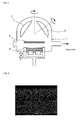
- Fig. 1 shows the schematic configuration of the off-axis sputtering system.
- the off-axis sputtering system includes a deposition chamber 1, a holder (substrate holder) 2 which is placed in the deposition chamber 1 and which holds a substrate (not shown) to be coated with the ZnO layer, a target 3 placed in the deposition chamber 1, and a shutter 4 placed between the target 2 and the substrate, which is held with the holder 2.
- the deposition chamber 1 is configured such that the deposition chamber 1 can be evacuated and the target 3 can be supplied with pulsed DC power.
- the off-axis sputtering system is configured such that the layer can be formed in such a state that the substrate, which has a surface for growing the layer, is placed outside a space which is located in the direction perpendicular to the target and in which high-energy particles come with high probability.
- the off-axis sputtering system is capable of forming the layer in such a manner that the composition of the layer is controlled such that the layer composition hardly differs from the composition of the target.
- the target 3 has a sintered density of 80% or more, a two-dimensional size of 315 mm ⁇ 118 mm, and a thickness of 5 mm.
- the substrate is made of at least one selected from the group consisting of glass, quartz, sapphire, Si, SiC, polyethylene terephthalate (PET), polyethylene naphthalate (PEN), polyethersulfone (PES), polyimide, cycloolefinic polymers, and polycarbonate. Even if the substrate is made of any one of the above materials, the substrate is surface-cleaned in advance of deposition in such a manner that the substrate is washed with isopropyl alcohol and irradiated with UV light.
- the substrate is set in the deposition chamber 1 of the off-axis sputtering system and the deposition chamber 1 is then evacuated to 5.5 ⁇ 10 -5 Pa. After evacuation, a high-purity Ar gas used as a sputtering gas is introduced into the deposition chamber 1 such that the pressure therein is increased to a predetermined value.
- the target 3 is sputtered in such a manner that a pulsed DC power with a predetermined pulse width is applied to the target 3 at a predetermined frequency.
- the thickness of a layer obtained by sputtering is set to 400 nm.
- the obtained ZnO layer is patterned by wet etching and then measured for thickness with a probe profilometer, whereby the ZnO layer is checked whether the ZnO layer has a set thickness.
- the ZnO layer is analyzed for composition, whereby the ZnO layer is checked whether the composition thereof is the same as that of the target.
- Layers prepared in examples or comparative examples each had a thickness substantially equal to a set thickness and the difference of the composition of each layer from that of a target was on an acceptable level.
- Variable sputtering conditions are principally the composition of the target (the type and dose of a group-III element), the type of the substrate, the pressure in the chamber, the rotation speed of the substrate, a pulsed DC power, a pulse width, and a pulse frequency.
- Fig. 2 is a cross-sectional SEM image of an Al-doped ZnO (AZO) layer, according to Example 1, having a granular crystal structure.
- the ZnO layer was prepared under conditions below.
- Target ZnO-mixed sintered body containing 3.0 weight percent Al 2 O 3
- Type of substrate alkali-free glass (Corning 1737)
- Pressure in chamber 0.1 Pa
- Rotation of substrate not rotated
- Pulsed DC power 2000 W
- Pulse width 2 ⁇ s Pulse frequency: 100 kHz
- the following layer was confirmed to have a granular crystal structure: a Ga-doped ZnO (GZO) layer, which is not shown, prepared using a ZnO-mixed sintered body containing 5.7 weight percent Ga 2 O 3 used as a target.
- GZO Ga-doped ZnO
- FIG. 3 is a cross-sectional SEM image of an Al-doped ZnO (AZO) layer, according to a comparative example, having a columnar crystal structure.
- AZO Al-doped ZnO
- GZO Ga-doped ZnO
- the ZnO layers according to the example and the comparative example were measured for resistivity by a four-probe technique.
- the ZnO layers according to the example and the comparative example were measured for sheet resistance.
- the ZnO layers according to the example and the comparative example were measured for transmittance at visible wavelengths. All the ZnO layers were confirmed to have a transmittance of 80% or more at visible wavelengths.
- Example 1 The ZnO layers according to Example 1 and Comparative Example, that is, the following layers were measured for change in resistivity with time in an atmosphere with a relative humidity of 85% at 85°C:
- Fig. 4 confirms that the granular crystalline region-including Al-doped ZnO (AZO) layer specified in Item (a) and the granular crystalline region-including Ga-doped ZnO (GZO) layer specified in Item (b) have a small change in resistivity with time and the columnar crystalline region-including Al-doped ZnO (AZO) layer specified in Item (c) and the columnar crystalline region-including Ga-doped ZnO (GZO) layer specified in Item (d), however, have a large change in resistivity with time.
- AZO Al-doped ZnO
- GZO Ga-doped ZnO
- Several types of targets having different Al 2 O 3 or Ga 2 O 3 contents were prepared. ZnO layers were formed under conditions similar to those described in Example 1 using the targets in such a manner that the dose of each group-III element was varied in four steps: 3.0, 5.7, 10.0, and 15.0 weight percent on an oxide mass basis. The obtained ZnO layers were used to investigate the relationship between the dose of the group-III element and the resistivity of the ZnO layers.
- Fig. 5 shows the data obtained using Al, which is a group-III element.
- a ZnO layer used as a transparent conductive film, for practical use has a resistivity of 1.2 ⁇ 10 -3 ⁇ cm or less.
- Fig. 5 confirms that the resistivity is 1.2 ⁇ 10 -3 ⁇ cm or less when the dose of the group-III element is within a range from 0.8 to 11.5 weight percent. Therefore, the dose of the group-III element is preferably within a range from 0.8 to 11.5 weight percent on an oxide mass basis.
- Fig. 5 shows the data obtained using Al, which is a group-III element.
- Example 2 confirms that the relationship between the dose of the group-III element and the resistivity of the ZnO layers does not significantly vary even if the group-III element is Al or Ga.
- the ZnO layers of Example 2 which are different in the dose of each group-III element from the ZnO layers of Example 1, are confirmed to have the granular crystal structure even if the dose of the group-III element is zero, although the crystal structures are not shown.
- Several types of targets having different Al 2 O 3 or Ga 2 O 3 contents were prepared in the same manner as that described in Example 2.
- ZnO layers were formed under conditions similar to those described in Example 1 using the targets in such a manner that the dose of each group-III element was varied in four steps: 3.0, 5.7, 10.0, and 15.0 weight percent on an oxide mass basis.
- the obtained ZnO layers were used to investigate the relationship between the dose of the group-III element and the full width at half maximum (FWHM) of the ZnO (002) rocking curve of each ZnO layer.
- Fig. 6 shows the data obtained using Al, which is a group-III element.
- Example 2 confirms that in order to allow the ZnO layers to have a resistivity suitable for use as transparent conductive films, the dose of the group-III element is preferably within a range from 0.8 to 11.5 weight percent on an oxide mass basis as described above.
- Example 3 ( Fig. 6 ) confirms that the full width at half maximum (FWHM) of the ZnO (002) rocking curve is preferably 10.5 degrees or less.
- Example 3 confirms that in order to allow the ZnO layers to have a resistivity of 1.2 ⁇ 10 -3 ⁇ cm suitable for use as transparent conductive films, the full width at half maximum (FWHM) of the ZnO (002) rocking curve is preferably 10.5 degrees or less.
- Fig. 6 shows the data obtained using Al, which is a group-III element.
- Example 3 confirms that the relationship between the dose and the full width at half maximum (FWHM) of the ZnO (002) rocking curve of each ZnO layer does not significantly vary even if the group-III element is Al or Ga.
- Substrates flexible substrates made of PEN (polyethylene naphthalate) were used instead of the glass substrate, made of alkali-free glass, used in Example 1.
- ZnO layers transparent conductive films
- Al or Ga are formed on the flexible substrates under the same conditions as those described in one of Examples 1 to 3 in the same manner as that described in one of Examples 1 to 3.
- the obtained ZnO layers were characterized under the same conditions as those described in one of the above examples. This confirmed that the ZnO layers (transparent conductive films) had substantially the same properties as those described in one of Examples 1 to 3.
- the ZnO layers (not shown) of Example 4 were confirmed to have a granular crystal structure. This confirms that a practical transparent conductive film can be formed on a substrate (flexible substrate) made of PEN (polyethylene naphthalate), which is versatile.
- Substrates flexible substrates made of PET (polyethylene terephthalate) were used instead of the glass substrate, made of alkali-free glass, used in Example 1.
- ZnO layers transparent conductive films
- Al or Ga are formed on the flexible substrates under the same conditions as those described in one of Examples 1 to 3 in the same manner as that described in one of Examples 1 to 3.
- the obtained ZnO layers were characterized under the same conditions as those described in one of the above examples. This confirmed that the ZnO layers (transparent conductive films) had substantially the same properties as those described in one of Examples 1 to 3.
- the ZnO layers of Example 5 were confirmed to have a granular crystal structure, although the crystal structures are not shown. This confirms that a practical transparent conductive film can be formed on a substrate (flexible substrate) made of PET (polyethylene terephthalate), which is versatile.
- the ZnO layers were formed on the glass substrates, the PEN substrates, or the PET substrates.
- a ZnO layer (transparent conductive film) according to the present invention may be formed on a single-crystalline substrate made of quartz, sapphire, or Si or a substrate made of SiC, polyethersulfone (PES), polyimide, a cycloolefinic polymer, or polycarbonate.
- PES polyethersulfone
- polyimide polyimide
- a cycloolefinic polymer or polycarbonate.
- the conditions described in Examples 1 to 5 are some of preferred exemplary conditions capable of efficiently growing granular crystals.
- conditions such as a chamber pressure, the dose of a group-III element and the type of a substrate are not dominant conditions in growing granular crystals.
- the conditions fixed through Examples 1 to 5 it is unclear that which condition is dominant.
- overall conditions including several sub-conditions probably need to be optimized. Even if the overall conditions are different from those described in Examples 1 to 5, granular crystals can be probably grown as long as the overall conditions are optimized.
- the present invention is not limited to the above examples.
- the followings may be variously adapted or modified within the scope of the present invention: the shape of a substrate for forming a ZnO layer (transparent conductive film), the type of a material for forming the substrate, the type and dose of a group-III element, and conditions for forming the ZnO layer.
- a ZnO-based transparent conductive film can be efficiently and securely produced.
- the ZnO-based transparent conductive film has humidity resistance sufficient for practical use and properties necessary for transparent conductive films and is cost-effective. Accordingly, the present invention can be widely used for various applications such as transparent electrodes for flat panel displays or solar cells.
Landscapes
- Chemical & Material Sciences (AREA)
- Engineering & Computer Science (AREA)
- Metallurgy (AREA)
- Chemical Kinetics & Catalysis (AREA)
- Materials Engineering (AREA)
- Mechanical Engineering (AREA)
- Organic Chemistry (AREA)
- Manufacturing & Machinery (AREA)
- Physical Vapour Deposition (AREA)
- Non-Insulated Conductors (AREA)
- Manufacturing Of Electric Cables (AREA)
- Conductive Materials (AREA)
- Inorganic Compounds Of Heavy Metals (AREA)
Abstract
Description
- The present invention relates to transparent conductive films and methods of producing the transparent conductive films. The present invention particularly relates to a transparent conductive film made of zinc oxide (ZnO) and a method of producing the transparent conductive film.
- In recent years, transparent electrodes have been widely used in flat panel displays and solar cells. The transparent electrodes are usually made of ITO (indium tin oxide).
- However, indium (In) is expensive and its resources seem to be exhausted. Therefore, there are increasing demands for transparent electrodes made of other materials. ZnO-based transparent electrodes, which are In-free transparent electrodes, are being developed because the ZnO-based transparent electrodes are made of the oxide (ZnO) of zinc (Zn), which is inexpensive and stably available.
- Although stoichiometric ZnO is an insulator, excess electrons due to oxygen defects and element replacement (doping) at a Zn site allow ZnO to be conductive. The following electrodes can be prepared at present: transparent electrodes which are made of such ZnO and which have a resistivity p in the order of 10-4 Ωcm.
- Conventional ZnO-based transparent conductive films have a problem in that the moisture resistance thereof is insufficient for practical use. That is, the conventional ZnO-based transparent conductive films contain a large number of oxygen defects and therefore have a problem in that the adsorption of moisture of the oxygen defects (reoxidation of the oxygen defects) reduces the number of carriers to cause an increase in resistance if the ZnO-based transparent conductive films are left in high-humidity environments. One of standards for the humidity resistance of an ITO transparent electrode is that the change in resistance of the ITO transparent electrode is ±10% after the ITO transparent electrode is left in an atmosphere with a relative humidity of 85% at 85°C for 720 h. However, no ZnO-based transparent conductive films meeting this standard have been obtained.
- If a ZnO-based transparent conductive film is formed on a flexible substrate, which may be used for various applications, there is a problem in that the transparent conductive film is seriously deteriorated by moisture because the flexible substrate is permeable to moisture and therefore not only the moisture present on a surface of the transparent conductive film but also the moisture passing through the flexible substrate affect the transparent conductive film.
- In order to solve the problems, various techniques for enhancing the moisture resistance of ZnO-based transparent conductive films have been investigated. The techniques are roughly categorized into the following two groups:
- (1) techniques for preventing moisture from passing through substrates using SiN barrier layers and
- (2) techniques for improving the quality (crystallinity) of ZnO films by heating.
However, no ZnO-based transparent conductive film with moisture resistance sufficient to for practical use has been obtained yet. - Proposed techniques for imparting conductivity to ZnO by element doping are as described below.
-
- (a) A technique in which the electrical resistance of a ZnO film is reduced with high controllability in such a manner that the ZnO film is doped with an impurity using a molecular beam of a group-IA element (H), a group-IIIA element (B, Al, Ga, or In), or a group-VIIA element (F, Cl, I, or Br) when the ZnO film is prepared using a molecular beam of ZnO or molecular beams of Zn and O (refer to Patent Document 1).
-
- (b) A transparent conductive body which contains ZnO doped with a group-VB or -VIB element in the periodic table and which includes a substrate and a transparent conductive film containing the element, the transparent conductive film being disposed on the substrate, the number of atoms of the element being 0.1% to 10% of the sum of the number of the element atoms and that of zinc atoms (refer to Patent Document 2).
-
- (c) An organic EL element which includes a substrate, an anode disposed on the substrate, a cathode, and an organic layer disposed between the anode and the cathode and in which the anode includes a transparent conductive film made of a material containing one or more of oxides of Ir, Mo, Mn, Nb, Os, Re, Ru, Rh, Cr, Fe, Pt, Ti, W, and V (refer to Patent Document 3).
-
- (d) A transistor including a transparent conductive material, such as conductive ZnO, doped or undoped with any one of group-II, -VII, -I, and -V elements (refer to Patent Document 4).
-
- (e) A transparent conductive film prepared by doping a zinc oxide thin film, having a c-axis/a-axis orientation ratio of 100 : 1 or more, with at least one of group- VII and - III compounds containing aluminum, gallium, or boron (refer to Patent Document 5).
-
- (f) An indium zinc oxide hexagonal layered compound which is represented by the formula (ZnO)m·In2O3 (m = 2 to 20), in which In or Zn is replaced with at least one selected from the group consisting of Sn, Y, Ho, Pb, Bi, Li, Al, Ga, Sb, Si, Cd, Mg, Co, Ni, Zr, Hf, Sc, Yb, Lu, Fe, Nb, Ta, W, Te, Au, Pt, and Ge, and which has an average thickness of 0.001 to 0.3 µm and an average aspect ratio (average major diameter/average thickness) of three to 1000 (refer to Patent Document 6).
- Known ZnO films which are formed by depositing zinc oxide particles prepared by oxidizing zinc particles generated by sputtering and which have columnar crystal structures (refer to Patent Document 7). Patent Document 7 discloses that the ZnO films each have a columnar crystal structure shown in Fig. 8 or 9 thereof. The reason why common ZnO films usually have a columnar crystal structure is probably that the (002) plane of a ZnO hexagonal crystal is extremely energetically stable and grains grow primarily at the (002) plane thereof.
- The known ZnO-based transparent conductive films have the above problems relating to moisture resistance.
- Under these circumstances, the present applicant has found that the crystal structure of ZnO has a significant effect on humidity resistance. The present applicant has proposed a transparent conductive film prepared by growing zinc oxide (ZnO) heavily doped with a group-III element on a substrate and a method of producing the transparent conductive film (refer to Patent Document 8). The transparent conductive film is different in configuration from that according to the present invention, is heavily doped with an impurity, has c-axes extending in different directions, and is excellent in humidity resistance.
- Patent Document 1: Japanese Unexamined Patent Application Publication No.
7-106615 - Patent Document 2: Japanese Unexamined Patent Application Publication No.
8-050815 - Patent Document 3: Japanese Unexamined Patent Application Publication No.
11-067459 - Patent Document 4: Japanese Unexamined Patent Application Publication No.
2000-150900 - Patent Document 5: Japanese Unexamined Patent Application Publication No.
2000-276943 - Patent Document 6:
WO 2001/056927 - Patent Document 7: Japanese Unexamined Patent Application Publication No.
2006-5115 - Patent Document 8:
WO 2007/080738 - The present invention has been made under the above circumstances. It is an object of the present invention to provide a ZnO-based transparent conductive film which is obtained by a method different from an impurity heavily doping method, which has humidity resistance sufficient for practical use and properties necessary for transparent conductive films, and which is cost-effective and to provide a method of producing the ZnO-based transparent conductive film.
- In order to solve the above problems, the inventors have formed various films by varying conditions using targets containing group-III elements. The inventors have found that a ZnO layer having a granular crystal structure different from a common columnar crystal structure is excellent in humidity resistance. The inventors have further performed experiments and investigations and have then completed the present invention.
A transparent conductive film according to the present invention (Claim 1) includes a zinc oxide (ZnO) layer grown on a substrate. The zinc oxide layer includes a region having a granular crystal structure. - In the transparent conductive film according to present invention, the zinc oxide layer is doped with a group-III element as described in
Claim 2. - In the transparent conductive film according to present invention, the dose of the group-III element is 0.8 to 11.5 weight percent on an oxide mass basis as described in
Claim 3. - In the transparent conductive film according to present invention, the full width at half maximum of a ZnO (002) rocking curve is preferably 10.5 degrees or less as described in
Claim 4. - In the transparent conductive film according to present invention, the substrate is made of at least one selected from the group consisting of glass, quartz, sapphire, Si, SiC, polyethylene terephthalate (PET), polyethylene naphthalate (PEN), polyethersulfone (PES), polyimide, cycloolefinic polymers, and polycarbonate as described in
Claim 5. - In the transparent conductive film according to present invention, the group-III element is at least one selected from the group consisting of Ga, Al, and In as described in Claim 6.
- A transparent conductive film according to the present invention includes a zinc oxide layer having a granular crystal structure. The transparent conductive film is grown on a substrate. This allows the transparent conductive film to have excellent humidity resistance and prevents the resistivity thereof from being deteriorated with time. A transparent conductive film having good humidity resistance stable properties can be obtained in such a manner that a ZnO layer is formed on a glass substrate by growing a granular crystal. The resistivity of this transparent conductive film hardly varies after a lapse of 200 hours even if the doping concentration of Al is low, for example, 3.0% by weight.
- The zinc oxide layer is doped with a group-III element as described in
Claim 2. This can securely provide a ZnO-based transparent conductive film which has humidity resistance sufficient for practical use and which is cost-effective. - The dose of the group-III element is 0.8 to 11.5 weight percent on an oxide mass basis as described in
Claim 3. Therefore, the following film can be securely achieved: a practical transparent conductive film which has excellent humidity resistance and of which the resistivity hardly varies with time. This proves the present invention to be effective. - A transparent conductive film is formed in such a manner that the doping concentration of the group-III element is controlled to be low such that the growth of C-axis columnar crystals is prevented and granular crystals are grown. Therefore, the following film can be securely achieved: a practical transparent conductive film which has low resistivity and excellent humidity resistance and of which the resistivity hardly varies with time.
When the dose of the group-III element is less than 0.8 weight percent or greater than 11.5 weight percent on an oxide mass basis, the resistivity is likely to be increased. Therefore, the dose of the group-III element is preferably 0.8 to 11.5 weight percent on an oxide mass basis. - The full width at half maximum of a ZnO (002) rocking curve is preferably 10.5 degrees or less as described in
Claim 4. Therefore, resistivity can be maintained low because the crystal orientation in grains is good. - The full width at half maximum of the ZnO (002) rocking curve correlates with the dose of the group-III element. When the dose of the group-III element is greater than 11.5 weight percent on an oxide mass basis, the full width at half maximum of the ZnO (002) rocking curve is greater than 10.5 degrees and resistivity is likely to increase. Therefore, the dose of the group-III element is preferably controlled such that the full width at half maximum of the ZnO (002) rocking curve does not exceed 10.5 degrees.
- In the transparent conductive film according to present invention, the substrate is made of at least one selected from the group consisting of glass, quartz, sapphire, Si, SiC, polyethylene terephthalate (PET), polyethylene naphthalate (PEN), polyethersulfone (PES), polyimide, cycloolefinic polymers, and polycarbonate as described in
Claim 5. The substrate can be used to form a ZnO-based transparent conductive film thereon. The ZnO-based transparent conductive film has humidity resistance sufficient for practical use and is cost-effective. - The group-III element is at least one selected from the group consisting of Ga, Al, and In as described in Claim 6. Therefore, the following film can be securely achieved: a ZnO-based transparent conductive film which has humidity resistance sufficient for practical use and which is cost-effective.
- In view of achieving sufficiently low resistivity, the group-III element (doping element) is most preferably Al or Ga. The use of In, which is another group-III element, is effective in achieving an advantage similar to that achieved by the use of Al or Ga.
-
- [
Fig. 1] Fig. 1 is a schematic view of an off-axis sputtering system used to form a ZnO layer, serving as a transparent conductive film, in an example (Example 1) of the present invention. - [
Fig. 2] Fig. 2 is a SEM image illustrating the crystal structure (a structure in which granular crystals are grown) of the ZnO layer (transparent conductive film) according to Example 1. - [
Fig. 3] Fig. 3 is a SEM image illustrating the crystal structure (a structure in which columnar crystals are grown) of a ZnO layer (transparent conductive film) according to a comparative example. - [
Fig. 4] Fig. 4 is a graph illustrating the temporal change in resistivity of each ZnO layer according to Example 1 and that of each ZnO layer according to the comparative example. - [
Fig. 5] Fig. 5 is a graph illustrating the relationship between the dose of a group-III element and the resistivity of each ZnO layer. - [
Fig. 6] Fig. 6 is a graph illustrating the relationship between the dose of a group-III element and the full width at half maximum (FWHM) of the ZnO (002) rocking curve of each ZnO layer. -
- 1
- deposition chamber
- 2
- holder (substrate holder)
- 3
- target
- 4
- shutter
- A transparent conductive film according to the present invention and a method of producing the transparent conductive film will now be described in detail.
- At first, the method of producing the transparent conductive film which includes a zinc oxide (ZnO) layer is described. The transparent conductive film is produced by using an off-axis sputtering system.
Fig. 1 shows the schematic configuration of the off-axis sputtering system. - The off-axis sputtering system includes a
deposition chamber 1, a holder (substrate holder) 2 which is placed in thedeposition chamber 1 and which holds a substrate (not shown) to be coated with the ZnO layer, atarget 3 placed in thedeposition chamber 1, and ashutter 4 placed between thetarget 2 and the substrate, which is held with theholder 2. Thedeposition chamber 1 is configured such that thedeposition chamber 1 can be evacuated and thetarget 3 can be supplied with pulsed DC power. - The off-axis sputtering system is configured such that the layer can be formed in such a state that the substrate, which has a surface for growing the layer, is placed outside a space which is located in the direction perpendicular to the target and in which high-energy particles come with high probability. The off-axis sputtering system is capable of forming the layer in such a manner that the composition of the layer is controlled such that the layer composition hardly differs from the composition of the target.
- The
target 3 has a sintered density of 80% or more, a two-dimensional size of 315 mm × 118 mm, and a thickness of 5 mm.
The substrate is made of at least one selected from the group consisting of glass, quartz, sapphire, Si, SiC, polyethylene terephthalate (PET), polyethylene naphthalate (PEN), polyethersulfone (PES), polyimide, cycloolefinic polymers, and polycarbonate. Even if the substrate is made of any one of the above materials, the substrate is surface-cleaned in advance of deposition in such a manner that the substrate is washed with isopropyl alcohol and irradiated with UV light. - The substrate is set in the
deposition chamber 1 of the off-axis sputtering system and thedeposition chamber 1 is then evacuated to 5.5 × 10⁻⁵ Pa.
After evacuation, a high-purity Ar gas used as a sputtering gas is introduced into thedeposition chamber 1 such that the pressure therein is increased to a predetermined value.
Thetarget 3 is sputtered in such a manner that a pulsed DC power with a predetermined pulse width is applied to thetarget 3 at a predetermined frequency. - The thickness of a layer obtained by sputtering is set to 400 nm. The obtained ZnO layer is patterned by wet etching and then measured for thickness with a probe profilometer, whereby the ZnO layer is checked whether the ZnO layer has a set thickness. The ZnO layer is analyzed for composition, whereby the ZnO layer is checked whether the composition thereof is the same as that of the target. Layers prepared in examples or comparative examples each had a thickness substantially equal to a set thickness and the difference of the composition of each layer from that of a target was on an acceptable level.
Variable sputtering conditions are principally the composition of the target (the type and dose of a group-III element), the type of the substrate, the pressure in the chamber, the rotation speed of the substrate, a pulsed DC power, a pulse width, and a pulse frequency. -
Fig. 2 is a cross-sectional SEM image of an Al-doped ZnO (AZO) layer, according to Example 1, having a granular crystal structure. The ZnO layer was prepared under conditions below.
Target: ZnO-mixed sintered body containing 3.0 weight percent Al2O3
Type of substrate: alkali-free glass (Corning 1737) Pressure in chamber: 0.1 Pa
Rotation of substrate: not rotated
Pulsed DC power: 2000 W
Pulse width: 2 µs
Pulse frequency: 100 kHz
The following layer was confirmed to have a granular crystal structure: a Ga-doped ZnO (GZO) layer, which is not shown, prepared using a ZnO-mixed sintered body containing 5.7 weight percent Ga2O3 used as a target. - A ZnO layer having a conventional columnar crystal structure was obtained under conditions partially different from the above conditions, for example, under such a condition that a substrate was rotated at 10 rpm.
Fig. 3 is a cross-sectional SEM image of an Al-doped ZnO (AZO) layer, according to a comparative example, having a columnar crystal structure. A Ga-doped ZnO (GZO) layer, which is not shown, was confirmed to have a columnar crystal structure. - As described above, it is found that slight changes in production conditions allow the obtained ZnO layers to have different crystal structures. However, it has not been sufficiently clear that what mechanism interrupts crystal growth on the (002) plane, which is extremely stable, to create a granular crystal structure.
- The ZnO layers according to the example and the comparative example were measured for resistivity by a four-probe technique.
- (1) Resistivity of ZnO layer according to Example 1
The resistivity of each ZnO layer formed as described above was confirmed to be a value below.
Resistivity of Al-doped ZnO (AZO) layer: 9.9 × 10⁻⁴ Ωcm
Resistivity of Ga-doped ZnO (GZO) layer: 7.1 × 10⁻⁴ Ωcm - (2) Resistivity of ZnO layer according to Comparative Example
The resistivity of each ZnO layer formed in the comparative example as described above was confirmed to be a value below.
Resistivity of Al-doped ZnO (AZO) layer: 9.3 × 10⁻⁴ Ωcm
Resistivity of Ga-doped ZnO (GZO) layer: 7.9 × 10⁻⁴ Ωcm - The ZnO layers according to the example and the comparative example were measured for sheet resistance.
- (1) Sheet resistance of ZnO layer according to Example 1
The sheet resistance of each ZnO layer formed in Example 1 as described above was confirmed to be a value below.
Sheet resistance of Al-doped ZnO (AZO) layer: 27 Ω/square
Sheet resistance of Ga-doped ZnO (GZO) layer: 19 Ω/square - (2) Sheet resistance of ZnO layer according to Comparative Example
The sheet resistance of each ZnO layer formed in the comparative example as described above was confirmed to be a value below.
Sheet resistance of Al-doped ZnO (AZO) layer: 23 Ω/square
Sheet resistance of Ga-doped ZnO (GZO) layer: 19 Ω/square - The ZnO layers according to the example and the comparative example were measured for transmittance at visible wavelengths. All the ZnO layers were confirmed to have a transmittance of 80% or more at visible wavelengths.
- The ZnO layers according to Example 1 and Comparative Example, that is, the following layers were measured for change in resistivity with time in an atmosphere with a relative humidity of 85% at 85°C:
- (a) the Al-doped ZnO (AZO) layer including the granular crystalline region,
- (b) the Ga-doped ZnO (GZO) layer including the granular crystalline region,
- (c) the Al-doped ZnO (AZO) layer including the columnar crystalline region, and
- (d) the Ga-doped ZnO (GZO) layer including the columnar crystalline region.
The measurement results are shown inFig. 4 . -
Fig. 4 confirms that the granular crystalline region-including Al-doped ZnO (AZO) layer specified in Item (a) and the granular crystalline region-including Ga-doped ZnO (GZO) layer specified in Item (b) have a small change in resistivity with time and the columnar crystalline region-including Al-doped ZnO (AZO) layer specified in Item (c) and the columnar crystalline region-including Ga-doped ZnO (GZO) layer specified in Item (d), however, have a large change in resistivity with time. - Several types of targets having different Al2O3 or Ga2O3 contents were prepared. ZnO layers were formed under conditions similar to those described in Example 1 using the targets in such a manner that the dose of each group-III element was varied in four steps: 3.0, 5.7, 10.0, and 15.0 weight percent on an oxide mass basis.
The obtained ZnO layers were used to investigate the relationship between the dose of the group-III element and the resistivity of the ZnO layers.Fig. 5 shows the data obtained using Al, which is a group-III element. - It is commonly known that a ZnO layer, used as a transparent conductive film, for practical use has a resistivity of 1.2 × 10⁻³ Ωcm or less.
Fig. 5 confirms that the resistivity is 1.2 × 10⁻³ Ωcm or less when the dose of the group-III element is within a range from 0.8 to 11.5 weight percent.
Therefore, the dose of the group-III element is preferably within a range from 0.8 to 11.5 weight percent on an oxide mass basis.
Fig. 5 shows the data obtained using Al, which is a group-III element. Example 2 confirms that the relationship between the dose of the group-III element and the resistivity of the ZnO layers does not significantly vary even if the group-III element is Al or Ga.
The ZnO layers of Example 2, which are different in the dose of each group-III element from the ZnO layers of Example 1, are confirmed to have the granular crystal structure even if the dose of the group-III element is zero, although the crystal structures are not shown. - Several types of targets having different Al2O3 or Ga2O3 contents were prepared in the same manner as that described in Example 2. ZnO layers were formed under conditions similar to those described in Example 1 using the targets in such a manner that the dose of each group-III element was varied in four steps: 3.0, 5.7, 10.0, and 15.0 weight percent on an oxide mass basis.
The obtained ZnO layers were used to investigate the relationship between the dose of the group-III element and the full width at half maximum (FWHM) of the ZnO (002) rocking curve of each ZnO layer.Fig. 6 shows the data obtained using Al, which is a group-III element. - Example 2 confirms that in order to allow the ZnO layers to have a resistivity suitable for use as transparent conductive films, the dose of the group-III element is preferably within a range from 0.8 to 11.5 weight percent on an oxide mass basis as described above. Example 3 (
Fig. 6 ) confirms that the full width at half maximum (FWHM) of the ZnO (002) rocking curve is preferably 10.5 degrees or less. - Example 3 confirms that in order to allow the ZnO layers to have a resistivity of 1.2 × 10⁻³ Ωcm suitable for use as transparent conductive films, the full width at half maximum (FWHM) of the ZnO (002) rocking curve is preferably 10.5 degrees or less.
Fig. 6 shows the data obtained using Al, which is a group-III element. Example 3 confirms that the relationship between the dose and the full width at half maximum (FWHM) of the ZnO (002) rocking curve of each ZnO layer does not significantly vary even if the group-III element is Al or Ga. - Substrates (flexible substrates) made of PEN (polyethylene naphthalate) were used instead of the glass substrate, made of alkali-free glass, used in Example 1. ZnO layers (transparent conductive films) doped with Al or Ga were formed on the flexible substrates under the same conditions as those described in one of Examples 1 to 3 in the same manner as that described in one of Examples 1 to 3.
- The obtained ZnO layers (transparent conductive films) were characterized under the same conditions as those described in one of the above examples. This confirmed that the ZnO layers (transparent conductive films) had substantially the same properties as those described in one of Examples 1 to 3.
The ZnO layers (not shown) of Example 4 were confirmed to have a granular crystal structure.
This confirms that a practical transparent conductive film can be formed on a substrate (flexible substrate) made of PEN (polyethylene naphthalate), which is versatile. - Substrates (flexible substrates) made of PET (polyethylene terephthalate) were used instead of the glass substrate, made of alkali-free glass, used in Example 1. ZnO layers (transparent conductive films) doped with Al or Ga were formed on the flexible substrates under the same conditions as those described in one of Examples 1 to 3 in the same manner as that described in one of Examples 1 to 3.
- The obtained ZnO layers (transparent conductive films) were characterized under the same conditions as those described in one of the above examples. This confirmed that the ZnO layers (transparent conductive films) had substantially the same properties as those described in one of Examples 1 to 3.
The ZnO layers of Example 5 were confirmed to have a granular crystal structure, although the crystal structures are not shown.
This confirms that a practical transparent conductive film can be formed on a substrate (flexible substrate) made of PET (polyethylene terephthalate), which is versatile. - In Examples 1 to 5, the ZnO layers (transparent conductive films) were formed on the glass substrates, the PEN substrates, or the PET substrates. A ZnO layer (transparent conductive film) according to the present invention may be formed on a single-crystalline substrate made of quartz, sapphire, or Si or a substrate made of SiC, polyethersulfone (PES), polyimide, a cycloolefinic polymer, or polycarbonate. The use of such a substrate can provide the same advantages as those obtained by the use of the glass substrates.
- The conditions described in Examples 1 to 5 are some of preferred exemplary conditions capable of efficiently growing granular crystals. Among conditions such as a chamber pressure, the dose of a group-III element and the type of a substrate are not dominant conditions in growing granular crystals. Among the conditions fixed through Examples 1 to 5, it is unclear that which condition is dominant. In order to grow granular crystals, overall conditions including several sub-conditions probably need to be optimized. Even if the overall conditions are different from those described in Examples 1 to 5, granular crystals can be probably grown as long as the overall conditions are optimized.
- The present invention is not limited to the above examples. The followings may be variously adapted or modified within the scope of the present invention: the shape of a substrate for forming a ZnO layer (transparent conductive film), the type of a material for forming the substrate, the type and dose of a group-III element, and conditions for forming the ZnO layer.
- As described above, according to the present invention, a ZnO-based transparent conductive film can be efficiently and securely produced. The ZnO-based transparent conductive film has humidity resistance sufficient for practical use and properties necessary for transparent conductive films and is cost-effective.
Accordingly, the present invention can be widely used for various applications such as transparent electrodes for flat panel displays or solar cells.
Claims (6)
- A transparent conductive film comprising a zinc oxide (ZnO) layer grown on a substrate, wherein the zinc oxide layer includes a region having a granular crystal structure.
- The transparent conductive film according to Claim 1, wherein the zinc oxide layer is doped with a group-III element.
- The transparent conductive film according to Claim 2, wherein the dose of the group-III element is 0.8 to 11.5 weight percent on an oxide mass basis.
- The transparent conductive film according to any one of Claims 1 to 3, wherein the full width at half maximum of a ZnO (002) rocking curve is preferably 10.5 degrees or less.
- The transparent conductive film according to any one of Claims 1 to 4, wherein the substrate is made of at least one selected from the group consisting of glass, quartz, sapphire, Si, SiC, polyethylene terephthalate (PET), polyethylene naphthalate (PEN), polyethersulfone (PES), polyimide, cycloolefinic polymers, and polycarbonate.
- The transparent conductive film according to any one of Claims 1 to 5, wherein the group-III element is at least one selected from the group consisting of Ga, Al, and In.
Applications Claiming Priority (2)
| Application Number | Priority Date | Filing Date | Title |
|---|---|---|---|
| JP2007230347 | 2007-09-05 | ||
| PCT/JP2008/064708 WO2009031399A1 (en) | 2007-09-05 | 2008-08-18 | Transparent conductive film and method for producing transparent conductive film |
Publications (2)
| Publication Number | Publication Date |
|---|---|
| EP2071586A1 true EP2071586A1 (en) | 2009-06-17 |
| EP2071586A4 EP2071586A4 (en) | 2014-03-05 |
Family
ID=40428720
Family Applications (1)
| Application Number | Title | Priority Date | Filing Date |
|---|---|---|---|
| EP08826879.2A Withdrawn EP2071586A4 (en) | 2007-09-05 | 2008-08-18 | TRANSPARENT CONDUCTIVE FILM AND METHOD OF MANUFACTURING THE SAME |
Country Status (7)
| Country | Link |
|---|---|
| US (1) | US20090269588A1 (en) |
| EP (1) | EP2071586A4 (en) |
| JP (1) | JP5040991B2 (en) |
| KR (1) | KR101041655B1 (en) |
| CN (1) | CN101548343A (en) |
| TW (1) | TWI453766B (en) |
| WO (1) | WO2009031399A1 (en) |
Families Citing this family (11)
| Publication number | Priority date | Publication date | Assignee | Title |
|---|---|---|---|---|
| KR101093424B1 (en) | 2009-11-10 | 2011-12-14 | 삼성모바일디스플레이주식회사 | Organic light emitting display device and manufacturing method thereof |
| JP5630747B2 (en) * | 2010-05-14 | 2014-11-26 | リンテック株式会社 | Zinc oxide-based conductive laminate, method for producing the same, and electronic device |
| JP5533448B2 (en) * | 2010-08-30 | 2014-06-25 | 住友金属鉱山株式会社 | Transparent conductive film laminate and manufacturing method thereof, thin film solar cell and manufacturing method thereof |
| JP2012144384A (en) * | 2011-01-07 | 2012-08-02 | Tokyo Institute Of Technology | Method for producing conductive zinc oxide film |
| KR101178496B1 (en) * | 2011-09-28 | 2012-09-07 | 한국에너지기술연구원 | Bilayered transparent conductive film and fabrication method of the same |
| WO2014058726A1 (en) * | 2012-10-08 | 2014-04-17 | Corning Incorporated | Sputtered transparent conductive aluminum doped zinc oxide films |
| TW201422835A (en) * | 2012-12-03 | 2014-06-16 | Solar Applied Mat Tech Corp | Sputtering target and conductive metal oxide film |
| JP6521390B2 (en) * | 2014-09-04 | 2019-05-29 | 日本碍子株式会社 | Zinc oxide sintered body and method for producing the same |
| JP2019098523A (en) * | 2017-11-28 | 2019-06-24 | 日本ゼオン株式会社 | Multilayer film for conductive film, and conductive film |
| CN114361267B (en) * | 2021-12-13 | 2024-08-09 | 中国科学院上海微系统与信息技术研究所 | SHJ solar cell double-layer TCO film structure and preparation method thereof |
| KR102919169B1 (en) * | 2023-10-18 | 2026-01-27 | 중앙대학교 산학협력단 | Highly transparent and highly conductive semiconductor substrate, method for manufacturing the same, and method for improving conductivity of the semiconductor substrate |
Family Cites Families (24)
| Publication number | Priority date | Publication date | Assignee | Title |
|---|---|---|---|---|
| US3471721A (en) * | 1966-10-25 | 1969-10-07 | Minnesota Mining & Mfg | Zinc oxide maximum efficiency length extensional crystals and devices |
| US3846649A (en) * | 1973-06-18 | 1974-11-05 | Rca Corp | Piezoelectric transducer comprising oriented zinc oxide film and method of manufacture |
| NL7908501A (en) * | 1979-11-22 | 1981-06-16 | Philips Nv | BODIES COMPOSED OF AT LEAST TWO PARTS, CONNECTING GLASS AND METHOD FOR ATTACHING PARTS TOGETHER. |
| JPH0731950B2 (en) * | 1985-11-22 | 1995-04-10 | 株式会社リコー | Method for producing transparent conductive film |
| JPH06248427A (en) * | 1993-02-26 | 1994-09-06 | Asahi Glass Co Ltd | Raw material for vacuum vapor deposition |
| EP0578046B1 (en) * | 1992-07-10 | 1996-11-06 | Asahi Glass Company Ltd. | Transparent conductive film, and target and material for vapor deposition to be used for its production |
| JP3453805B2 (en) * | 1992-09-11 | 2003-10-06 | 旭硝子株式会社 | Transparent conductive film |
| JPH07249316A (en) * | 1994-03-10 | 1995-09-26 | Asahi Glass Co Ltd | Transparent conductive film and transparent substrate using the transparent conductive film |
| DE69702277T2 (en) * | 1996-03-06 | 2001-03-01 | Canon K.K., Tokio/Tokyo | A method of manufacturing a thin zinc oxide film and a method of manufacturing a substrate of a semiconductor device, and a method of manufacturing a photoelectric conversion device using this film |
| JP4663829B2 (en) * | 1998-03-31 | 2011-04-06 | 三菱電機株式会社 | Thin film transistor and liquid crystal display device using the thin film transistor |
| JP3276930B2 (en) * | 1998-11-17 | 2002-04-22 | 科学技術振興事業団 | Transistor and semiconductor device |
| JP2000276943A (en) * | 1999-03-26 | 2000-10-06 | Tohoku Ricoh Co Ltd | Transparent conductive film |
| KR20020003558A (en) * | 2000-02-04 | 2002-01-12 | 오츠카 유지로 | Hexagonal lamellar compound based on indium-zinc oxide and process for producing the same |
| JP4622075B2 (en) * | 2000-10-03 | 2011-02-02 | 凸版印刷株式会社 | Transparent conductive material and method for producing the same |
| US7118936B2 (en) * | 2001-10-11 | 2006-10-10 | Bridgestone Corporation | Organic dye-sensitized metal oxide semiconductor electrode and its manufacturing method, and organic dye-sensitized solar cell |
| JP3749498B2 (en) * | 2002-03-26 | 2006-03-01 | スタンレー電気株式会社 | Crystal growth substrate and ZnO-based compound semiconductor device |
| JP4277506B2 (en) * | 2002-10-24 | 2009-06-10 | 株式会社村田製作所 | ZnO-based thin film for thermoelectric material of thermoelectric conversion element, thermoelectric conversion element using the ZnO-based thin film, and infrared sensor |
| KR100968560B1 (en) * | 2003-01-07 | 2010-07-08 | 삼성전자주식회사 | Metal wiring formation method of thin film transistor substrate and thin film transistor substrate |
| CN1278385C (en) * | 2003-03-25 | 2006-10-04 | 浙江大学 | P-ZnO thin film and preparation thereof |
| JP2004296616A (en) * | 2003-03-26 | 2004-10-21 | Canon Inc | Photovoltaic element |
| US6946928B2 (en) * | 2003-10-30 | 2005-09-20 | Agilent Technologies, Inc. | Thin-film acoustically-coupled transformer |
| KR100945199B1 (en) * | 2005-12-22 | 2010-03-03 | 미츠이 긴조쿠 고교 가부시키가이샤 | Patterning method of zinc oxide transparent conductive film |
| US7867636B2 (en) * | 2006-01-11 | 2011-01-11 | Murata Manufacturing Co., Ltd. | Transparent conductive film and method for manufacturing the same |
| KR101057571B1 (en) * | 2007-02-26 | 2011-08-17 | 가부시키가이샤 무라타 세이사쿠쇼 | Conductive film and manufacturing method of the conductive film |
-
2008
- 2008-08-18 WO PCT/JP2008/064708 patent/WO2009031399A1/en not_active Ceased
- 2008-08-18 EP EP08826879.2A patent/EP2071586A4/en not_active Withdrawn
- 2008-08-18 KR KR1020097006617A patent/KR101041655B1/en not_active Expired - Fee Related
- 2008-08-18 CN CNA2008800008896A patent/CN101548343A/en active Pending
- 2008-08-18 JP JP2009504162A patent/JP5040991B2/en not_active Expired - Fee Related
- 2008-08-21 TW TW97131963A patent/TWI453766B/en not_active IP Right Cessation
-
2009
- 2009-07-10 US US12/500,694 patent/US20090269588A1/en not_active Abandoned
Also Published As
| Publication number | Publication date |
|---|---|
| TWI453766B (en) | 2014-09-21 |
| JP5040991B2 (en) | 2012-10-03 |
| US20090269588A1 (en) | 2009-10-29 |
| KR101041655B1 (en) | 2011-06-14 |
| JPWO2009031399A1 (en) | 2010-12-09 |
| TW200929268A (en) | 2009-07-01 |
| KR20090094067A (en) | 2009-09-03 |
| CN101548343A (en) | 2009-09-30 |
| EP2071586A4 (en) | 2014-03-05 |
| WO2009031399A1 (en) | 2009-03-12 |
Similar Documents
| Publication | Publication Date | Title |
|---|---|---|
| EP2071586A1 (en) | Transparent conductive film and method for producing transparent conductive film | |
| JP5181677B2 (en) | Transparent conductive film | |
| EP2061041A1 (en) | Conductive film and method for production of conductive film | |
| US8303856B2 (en) | Conductive laminated body and method for preparing the same | |
| CN107074662B (en) | Metal oxide thin film, method for depositing metal oxide thin film, and apparatus including metal oxide thin film | |
| CN105845196B (en) | Manganese tin-oxide class transparent conductive oxide and using its multi-layer transparent conductive film with and preparation method thereof | |
| US20170175249A1 (en) | Thin metal film substrate and method for preparing the same | |
| JP6709171B2 (en) | Transparent conductive film and method for producing transparent conductive film | |
| KR102164629B1 (en) | Composite transparent electrodes | |
| JP4170507B2 (en) | Method for producing transparent conductive film | |
| KR101005973B1 (en) | Conductive laminate and method for manufacturing same | |
| JP5632135B2 (en) | Method for forming ZnO film | |
| KR101807957B1 (en) | Highly conductive flexible transparent electrodes based oxide and method for manufacturing thereof | |
| TW202332581A (en) | Laminate having function as transparent conductive film, method for producing same, and oxide sputtering target for producing laminate | |
| CN117280428A (en) | A laminated body having a function as a transparent conductive film, a manufacturing method thereof, and an oxide sputtering target for manufacturing the laminated body |
Legal Events
| Date | Code | Title | Description |
|---|---|---|---|
| PUAI | Public reference made under article 153(3) epc to a published international application that has entered the european phase |
Free format text: ORIGINAL CODE: 0009012 |
|
| 17P | Request for examination filed |
Effective date: 20090203 |
|
| AK | Designated contracting states |
Kind code of ref document: A1 Designated state(s): AT BE BG CH CY CZ DE DK EE ES FI FR GB GR HR HU IE IS IT LI LT LU LV MC MT NL NO PL PT RO SE SI SK TR |
|
| AX | Request for extension of the european patent |
Extension state: AL BA MK RS |
|
| DAX | Request for extension of the european patent (deleted) | ||
| A4 | Supplementary search report drawn up and despatched |
Effective date: 20140205 |
|
| RIC1 | Information provided on ipc code assigned before grant |
Ipc: C23C 14/34 20060101ALI20140130BHEP Ipc: C23C 14/08 20060101AFI20140130BHEP |
|
| STAA | Information on the status of an ep patent application or granted ep patent |
Free format text: STATUS: THE APPLICATION IS DEEMED TO BE WITHDRAWN |
|
| 18D | Application deemed to be withdrawn |
Effective date: 20180301 |