EP2063465A1 - Process for producing semiconductor device - Google Patents
Process for producing semiconductor device Download PDFInfo
- Publication number
- EP2063465A1 EP2063465A1 EP07792087A EP07792087A EP2063465A1 EP 2063465 A1 EP2063465 A1 EP 2063465A1 EP 07792087 A EP07792087 A EP 07792087A EP 07792087 A EP07792087 A EP 07792087A EP 2063465 A1 EP2063465 A1 EP 2063465A1
- Authority
- EP
- European Patent Office
- Prior art keywords
- adhesive layer
- wiring board
- present
- chip
- die
- Prior art date
- Legal status (The legal status is an assumption and is not a legal conclusion. Google has not performed a legal analysis and makes no representation as to the accuracy of the status listed.)
- Withdrawn
Links
Images
Classifications
-
- H—ELECTRICITY
- H10—SEMICONDUCTOR DEVICES; ELECTRIC SOLID-STATE DEVICES NOT OTHERWISE PROVIDED FOR
- H10P—GENERIC PROCESSES OR APPARATUS FOR THE MANUFACTURE OR TREATMENT OF DEVICES COVERED BY CLASS H10
- H10P72/00—Handling or holding of wafers, substrates or devices during manufacture or treatment thereof
- H10P72/70—Handling or holding of wafers, substrates or devices during manufacture or treatment thereof for supporting or gripping
- H10P72/74—Handling or holding of wafers, substrates or devices during manufacture or treatment thereof for supporting or gripping using temporarily an auxiliary support
- H10P72/7402—Wafer tapes, e.g. grinding or dicing support tapes
-
- H—ELECTRICITY
- H10—SEMICONDUCTOR DEVICES; ELECTRIC SOLID-STATE DEVICES NOT OTHERWISE PROVIDED FOR
- H10W—GENERIC PACKAGES, INTERCONNECTIONS, CONNECTORS OR OTHER CONSTRUCTIONAL DETAILS OF DEVICES COVERED BY CLASS H10
- H10W95/00—Packaging processes not covered by the other groups of this subclass
-
- H—ELECTRICITY
- H10—SEMICONDUCTOR DEVICES; ELECTRIC SOLID-STATE DEVICES NOT OTHERWISE PROVIDED FOR
- H10W—GENERIC PACKAGES, INTERCONNECTIONS, CONNECTORS OR OTHER CONSTRUCTIONAL DETAILS OF DEVICES COVERED BY CLASS H10
- H10W72/00—Interconnections or connectors in packages
- H10W72/071—Connecting or disconnecting
-
- H—ELECTRICITY
- H10—SEMICONDUCTOR DEVICES; ELECTRIC SOLID-STATE DEVICES NOT OTHERWISE PROVIDED FOR
- H10W—GENERIC PACKAGES, INTERCONNECTIONS, CONNECTORS OR OTHER CONSTRUCTIONAL DETAILS OF DEVICES COVERED BY CLASS H10
- H10W72/00—Interconnections or connectors in packages
- H10W72/30—Die-attach connectors
-
- H—ELECTRICITY
- H10—SEMICONDUCTOR DEVICES; ELECTRIC SOLID-STATE DEVICES NOT OTHERWISE PROVIDED FOR
- H10P—GENERIC PROCESSES OR APPARATUS FOR THE MANUFACTURE OR TREATMENT OF DEVICES COVERED BY CLASS H10
- H10P72/00—Handling or holding of wafers, substrates or devices during manufacture or treatment thereof
- H10P72/70—Handling or holding of wafers, substrates or devices during manufacture or treatment thereof for supporting or gripping
- H10P72/74—Handling or holding of wafers, substrates or devices during manufacture or treatment thereof for supporting or gripping using temporarily an auxiliary support
- H10P72/7416—Handling or holding of wafers, substrates or devices during manufacture or treatment thereof for supporting or gripping using temporarily an auxiliary support used during dicing or grinding
-
- H—ELECTRICITY
- H10—SEMICONDUCTOR DEVICES; ELECTRIC SOLID-STATE DEVICES NOT OTHERWISE PROVIDED FOR
- H10P—GENERIC PROCESSES OR APPARATUS FOR THE MANUFACTURE OR TREATMENT OF DEVICES COVERED BY CLASS H10
- H10P72/00—Handling or holding of wafers, substrates or devices during manufacture or treatment thereof
- H10P72/70—Handling or holding of wafers, substrates or devices during manufacture or treatment thereof for supporting or gripping
- H10P72/74—Handling or holding of wafers, substrates or devices during manufacture or treatment thereof for supporting or gripping using temporarily an auxiliary support
- H10P72/7438—Handling or holding of wafers, substrates or devices during manufacture or treatment thereof for supporting or gripping using temporarily an auxiliary support with parts of the auxiliary support remaining in the finished device
-
- H—ELECTRICITY
- H10—SEMICONDUCTOR DEVICES; ELECTRIC SOLID-STATE DEVICES NOT OTHERWISE PROVIDED FOR
- H10P—GENERIC PROCESSES OR APPARATUS FOR THE MANUFACTURE OR TREATMENT OF DEVICES COVERED BY CLASS H10
- H10P72/00—Handling or holding of wafers, substrates or devices during manufacture or treatment thereof
- H10P72/70—Handling or holding of wafers, substrates or devices during manufacture or treatment thereof for supporting or gripping
- H10P72/74—Handling or holding of wafers, substrates or devices during manufacture or treatment thereof for supporting or gripping using temporarily an auxiliary support
- H10P72/744—Details of chemical or physical process used for separating the auxiliary support from a device or a wafer
-
- H—ELECTRICITY
- H10—SEMICONDUCTOR DEVICES; ELECTRIC SOLID-STATE DEVICES NOT OTHERWISE PROVIDED FOR
- H10W—GENERIC PACKAGES, INTERCONNECTIONS, CONNECTORS OR OTHER CONSTRUCTIONAL DETAILS OF DEVICES COVERED BY CLASS H10
- H10W72/00—Interconnections or connectors in packages
- H10W72/01—Manufacture or treatment
- H10W72/013—Manufacture or treatment of die-attach connectors
- H10W72/01331—Manufacture or treatment of die-attach connectors using blanket deposition
- H10W72/01336—Manufacture or treatment of die-attach connectors using blanket deposition in solid form, e.g. by using a powder or by laminating a foil
-
- H—ELECTRICITY
- H10—SEMICONDUCTOR DEVICES; ELECTRIC SOLID-STATE DEVICES NOT OTHERWISE PROVIDED FOR
- H10W—GENERIC PACKAGES, INTERCONNECTIONS, CONNECTORS OR OTHER CONSTRUCTIONAL DETAILS OF DEVICES COVERED BY CLASS H10
- H10W72/00—Interconnections or connectors in packages
- H10W72/071—Connecting or disconnecting
- H10W72/072—Connecting or disconnecting of bump connectors
- H10W72/07231—Techniques
- H10W72/07236—Soldering or alloying
-
- H—ELECTRICITY
- H10—SEMICONDUCTOR DEVICES; ELECTRIC SOLID-STATE DEVICES NOT OTHERWISE PROVIDED FOR
- H10W—GENERIC PACKAGES, INTERCONNECTIONS, CONNECTORS OR OTHER CONSTRUCTIONAL DETAILS OF DEVICES COVERED BY CLASS H10
- H10W72/00—Interconnections or connectors in packages
- H10W72/071—Connecting or disconnecting
- H10W72/072—Connecting or disconnecting of bump connectors
- H10W72/07251—Connecting or disconnecting of bump connectors characterised by changes in properties of the bump connectors during connecting
-
- H—ELECTRICITY
- H10—SEMICONDUCTOR DEVICES; ELECTRIC SOLID-STATE DEVICES NOT OTHERWISE PROVIDED FOR
- H10W—GENERIC PACKAGES, INTERCONNECTIONS, CONNECTORS OR OTHER CONSTRUCTIONAL DETAILS OF DEVICES COVERED BY CLASS H10
- H10W72/00—Interconnections or connectors in packages
- H10W72/071—Connecting or disconnecting
- H10W72/073—Connecting or disconnecting of die-attach connectors
-
- H—ELECTRICITY
- H10—SEMICONDUCTOR DEVICES; ELECTRIC SOLID-STATE DEVICES NOT OTHERWISE PROVIDED FOR
- H10W—GENERIC PACKAGES, INTERCONNECTIONS, CONNECTORS OR OTHER CONSTRUCTIONAL DETAILS OF DEVICES COVERED BY CLASS H10
- H10W72/00—Interconnections or connectors in packages
- H10W72/071—Connecting or disconnecting
- H10W72/073—Connecting or disconnecting of die-attach connectors
- H10W72/07331—Connecting techniques
- H10W72/07337—Connecting techniques using a polymer adhesive, e.g. an adhesive based on silicone or epoxy
- H10W72/07338—Connecting techniques using a polymer adhesive, e.g. an adhesive based on silicone or epoxy hardening the adhesive by curing, e.g. thermosetting
-
- H—ELECTRICITY
- H10—SEMICONDUCTOR DEVICES; ELECTRIC SOLID-STATE DEVICES NOT OTHERWISE PROVIDED FOR
- H10W—GENERIC PACKAGES, INTERCONNECTIONS, CONNECTORS OR OTHER CONSTRUCTIONAL DETAILS OF DEVICES COVERED BY CLASS H10
- H10W72/00—Interconnections or connectors in packages
- H10W72/071—Connecting or disconnecting
- H10W72/075—Connecting or disconnecting of bond wires
-
- H—ELECTRICITY
- H10—SEMICONDUCTOR DEVICES; ELECTRIC SOLID-STATE DEVICES NOT OTHERWISE PROVIDED FOR
- H10W—GENERIC PACKAGES, INTERCONNECTIONS, CONNECTORS OR OTHER CONSTRUCTIONAL DETAILS OF DEVICES COVERED BY CLASS H10
- H10W72/00—Interconnections or connectors in packages
- H10W72/20—Bump connectors, e.g. solder bumps or copper pillars; Dummy bumps; Thermal bumps
-
- H—ELECTRICITY
- H10—SEMICONDUCTOR DEVICES; ELECTRIC SOLID-STATE DEVICES NOT OTHERWISE PROVIDED FOR
- H10W—GENERIC PACKAGES, INTERCONNECTIONS, CONNECTORS OR OTHER CONSTRUCTIONAL DETAILS OF DEVICES COVERED BY CLASS H10
- H10W72/00—Interconnections or connectors in packages
- H10W72/30—Die-attach connectors
- H10W72/351—Materials of die-attach connectors
- H10W72/352—Materials of die-attach connectors comprising metals or metalloids, e.g. solders
-
- H—ELECTRICITY
- H10—SEMICONDUCTOR DEVICES; ELECTRIC SOLID-STATE DEVICES NOT OTHERWISE PROVIDED FOR
- H10W—GENERIC PACKAGES, INTERCONNECTIONS, CONNECTORS OR OTHER CONSTRUCTIONAL DETAILS OF DEVICES COVERED BY CLASS H10
- H10W72/00—Interconnections or connectors in packages
- H10W72/30—Die-attach connectors
- H10W72/351—Materials of die-attach connectors
- H10W72/353—Materials of die-attach connectors not comprising solid metals or solid metalloids, e.g. ceramics
- H10W72/354—Materials of die-attach connectors not comprising solid metals or solid metalloids, e.g. ceramics comprising polymers
-
- H—ELECTRICITY
- H10—SEMICONDUCTOR DEVICES; ELECTRIC SOLID-STATE DEVICES NOT OTHERWISE PROVIDED FOR
- H10W—GENERIC PACKAGES, INTERCONNECTIONS, CONNECTORS OR OTHER CONSTRUCTIONAL DETAILS OF DEVICES COVERED BY CLASS H10
- H10W72/00—Interconnections or connectors in packages
- H10W72/851—Dispositions of multiple connectors or interconnections
- H10W72/874—On different surfaces
- H10W72/884—Die-attach connectors and bond wires
-
- H—ELECTRICITY
- H10—SEMICONDUCTOR DEVICES; ELECTRIC SOLID-STATE DEVICES NOT OTHERWISE PROVIDED FOR
- H10W—GENERIC PACKAGES, INTERCONNECTIONS, CONNECTORS OR OTHER CONSTRUCTIONAL DETAILS OF DEVICES COVERED BY CLASS H10
- H10W74/00—Encapsulations, e.g. protective coatings
-
- H—ELECTRICITY
- H10—SEMICONDUCTOR DEVICES; ELECTRIC SOLID-STATE DEVICES NOT OTHERWISE PROVIDED FOR
- H10W—GENERIC PACKAGES, INTERCONNECTIONS, CONNECTORS OR OTHER CONSTRUCTIONAL DETAILS OF DEVICES COVERED BY CLASS H10
- H10W74/00—Encapsulations, e.g. protective coatings
- H10W74/10—Encapsulations, e.g. protective coatings characterised by their shape or disposition
- H10W74/15—Encapsulations, e.g. protective coatings characterised by their shape or disposition on active surfaces of flip-chip devices, e.g. underfills
-
- H—ELECTRICITY
- H10—SEMICONDUCTOR DEVICES; ELECTRIC SOLID-STATE DEVICES NOT OTHERWISE PROVIDED FOR
- H10W—GENERIC PACKAGES, INTERCONNECTIONS, CONNECTORS OR OTHER CONSTRUCTIONAL DETAILS OF DEVICES COVERED BY CLASS H10
- H10W90/00—Package configurations
-
- H—ELECTRICITY
- H10—SEMICONDUCTOR DEVICES; ELECTRIC SOLID-STATE DEVICES NOT OTHERWISE PROVIDED FOR
- H10W—GENERIC PACKAGES, INTERCONNECTIONS, CONNECTORS OR OTHER CONSTRUCTIONAL DETAILS OF DEVICES COVERED BY CLASS H10
- H10W90/00—Package configurations
- H10W90/701—Package configurations characterised by the relative positions of pads or connectors relative to package parts
- H10W90/731—Package configurations characterised by the relative positions of pads or connectors relative to package parts of die-attach connectors
- H10W90/734—Package configurations characterised by the relative positions of pads or connectors relative to package parts of die-attach connectors between a chip and a stacked insulating package substrate, interposer or RDL
Definitions
- the present invention relates to a process for manufacturing semiconductor devices. More particularly, the invention relates to a process for manufacturing semiconductor devices by heating a wiring board on which chips are mounted via an uncured adhesive layer to cure the adhesive layer.
- chips are die-bonded to a wiring board with a liquid thermosetting adhesive or a film thermosetting adhesive (die-bonding step), then wires are bonded (wire-bonding step), and the chips are encapsulated (encapsulating step) ( Fig. 4 , V to VII).
- a chip 2 is mounted on a wiring board 4 via an uncured adhesive layer 3
- voids 5 are often formed in the adhesive, or voids 6 may be produced in an interface between the adhesive and the chip or the wiring board ( Fig. 4 ).
- Such voids do not disappear and remain after the die-bonding step ( Fig. 4 ).
- the use of a liquid adhesive frequently results in voids in the adhesive, and the use of a film adhesive often results in voids in the interface due to insufficient adhesion and insufficient followability to unevenness of an adherend surface.
- Patent Document 1 improves the followability to unevenness of a wiring board by reducing the viscosity of a liquid adhesive applied, or by reducing the elastic modulus of a film adhesive used in the die-bonding or optimizing die-bonding conditions.
- the above method can decrease voids in liquid adhesives or films adhesive, reducing the viscosity or the elastic modulus is accompanied by a problem that the adhesive squeezes out to edges of a die-bonded chip. Because chips are getting thinner in recent years, the adhesive that has squeezed out curls up onto the circuit surface of the chip to contaminate wire pads and reduce the bond strength of wires.
- the present inventors have diligently studied and have found that the above problems are solved by performing a specific statically pressurizing step.
- the present invention has been completed based on the finding.
- the improvement of the present invention comprises performing a statically pressurizing step before the adhesive layer is cured (the curing reaction has completed), in which step the wiring board on which the chip and the uncured adhesive layer are laminated is subjected to a static pressure greater than atmospheric pressure by not less than 0.05 MPa.
- the improvement preferably comprises performing a heat curing step in which the wiring board on which the chip and the uncured adhesive layer are laminated is heated to cure the adhesive layer while maintaining the static pressure applied in the statically pressurizing step.
- a chip is mounted on a wiring board via an uncured adhesive layer under usual conditions, and voids are easily eliminated in the subsequent statically pressurizing step irrespective of the design of the wiring board. Because the pressure applied to the wiring board in the statically pressurizing step is static, the adhesive does not curl up.
- a wiring board 1 on which a chip 2 and an uncured adhesive layer 3 are laminated (a wiring board 1 on which a chip 2 is die-bonded through an uncured adhesive layer 3, the same applies hereinafter) is heated to cure the uncured adhesive layer 3.
- a semiconductor device is thus manufactured ( Fig. 1 ).
- the adhesive layer is sufficiently cured.
- the chips 2 are obtained by cutting a semiconductor wafer with respect to respective circuits.
- Examples of the wiring boards 4 include lead frames of metals, boards of organic or inorganic materials, and laminates of metals and organic or inorganic materials.
- a multi-stack semiconductor device is manufactured, a relatively lower chip is regarded as part of a wiring board.
- the uncured adhesive layer 3 is a film adhesive or a liquid adhesive, and is preferably a film adhesive.
- the adhesive used in the invention is a thermosetting adhesive which contains a thermosetting resin.
- the thermosetting resins include epoxy resins, phenoxy resins, phenol resins, resorcinol resins, urea resins, melamine resins, furane resins, unsaturated polyester resins and silicone resins.
- the thermosetting resin is used in combination with an appropriate curing agent and an optional curing accelerator. Conventional thermosetting resins may be used in the invention without limitation.
- the thermosetting adhesive may be a sticky adhesive that shows stickiness at ordinary temperature.
- the sticky adhesive used herein is an adhesive that shows stickiness at ordinary temperature in an initial state and shows strong adhesion when cured by a trigger such as heat.
- Examples of the sticky adhesives include mixtures of binder resins showing pressure sensitive adhesion at ordinary temperature and the above-mentioned thermosetting resins.
- Examples of the binder resins showing pressure sensitive adhesion at ordinary temperature include acrylic resins, polyester resins, polyvinyl ether resins, urethane resins and polyamide resins.
- a dicing/die-bonding sheet having a film adhesive layer may be used.
- the dicing/die-bonding sheet includes a base film and a film adhesive layer of the above composition that is releasably laminated on the base film.
- the releasability of the film adhesive layer from the base film may be preferably controlled by incorporating an energy ray curable resin such as a urethane acrylate oligomer in the adhesive of the film adhesive layer.
- the adhesive containing the energy ray curable resin shows high adhesion to the base film before energy ray irradiation and is easily released from the base film after the energy ray irradiation.
- the thickness of the film adhesive layer in the dicing/die-bonding sheet is variable depending on the level and shape of unevenness of a wiring board that is an adherend.
- the thickness is generally in the range of 3 to 100 ⁇ m, preferably 10 to 50 ⁇ m.
- the process for manufacturing a semiconductor device includes (1) a dicing step (1), a die-bonding step (2), a statically pressurizing step (3), a heat curing step (4), and an assembling step (5).
- a dicing/die-bonding sheet is applied to a wafer such as silicon, and the wafer and an uncured adhesive layer are diced.
- the resultant chips have the uncured adhesive layer on one surface.
- an energy ray may be applied before or after the dicing step to reduce the adhesion to a base film.
- voids may form in the interface between the chip and the uncured adhesive layer.
- the chips are released (picked up) from the base film at the interface between the base film and the uncured adhesive layer 3, and the chips having the uncured adhesive layer are mounted (die-bonded) on chip-mounting parts of a wiring board. Consequently, a wiring board 1 is obtained on which the chips 2 are mounted through the uncured adhesive layer 3.
- voids 6 may form in the interface between the uncured adhesive layer 3 and the wiring board 4 ( Fig. 1 ).
- a pressure (static pressure) is uniformly applied in all directions to the wiring board on which the chips are die-bonded, before the uncured adhesive layer is sufficiently cured ( Fig. 1 , I).
- the pressure is greater than atmospheric pressure by not less than 0.05 MPa, preferably by 0.1 to 1.0 MPa. That is, the pressure applied in the invention surpasses atmospheric pressure by not less than 0.05 MPa, preferably by 0.1 to 1.0 MPa.
- the statically pressurizing step is performed as follows.
- the wiring board 1 on which the chips 2 are die-bonded through the uncured adhesive layer 3 is subjected to the static pressure ( Fig. 1 , I).
- the application of the static pressure removes voids (not shown) between the adhesive layer 3 and the chip 2 or voids 6 between the adhesive layer 3 and the wiring board 4.
- the voids 6 are easily removed without controlling conditions under which the chips 2 are mounted on the wiring board 4 through the uncured adhesive layer 3.
- the static pressure applied in the statically pressurizing step pressurizes the laminate uniformly in all directions and prevents the adhesive from squeezing out and curling up.
- the pressure in the range as described above can efficiently eliminate the voids and can be applied by general-purpose pressurizing apparatuses and pressure-resistant explosion-proof equipment, enabling a compact production line.
- the pressure in the above range is also advantageous in that it can be reached immediately.
- the pressurizing time is preferably in the range of 1 to 120 minutes, more preferably 5 to 90 minutes.
- the statically pressurizing apparatus used in the invention is not particularly limited as long as it can apply a static pressure to the wiring board 1 on which the chips are die-bonded.
- Preferred examples of the pressurizing apparatuses include autoclaves (pressure tight cases with a compressor). Increasing the pressure in an autoclave having a fixed volume results in an elevated temperature of the atmosphere. Because the temperature is preferably constant for stable production of semiconductor devices, the temperature may be controlled while avoiding the curing of the adhesive layer 3. At controlled high temperatures, the adhesive layer is fluidized to permit the voids to move easily, and the voids may be eliminated easily. The temperature may be controlled appropriately depending on the composition of the adhesive of the adhesive layer 3, and is for example in the range of about 30 to 120°C.
- the uncured adhesive layer 3 of the wiring board 1 is sufficiently cured by heating ( Fig. 1 , II).
- the term "uncured” means that curing reaction has not proceeded in the adhesive, and the term “sufficiently cured” means that the curing reaction has completed and the adhesive is not deformed.
- the wiring board 1 from which the voids are eliminated in the statically pressurizing step (3) is removed from the pressurizing apparatus and is introduced into a heating apparatus in which the pressure is atmospheric.
- the uncured adhesive layer 3 is cured to give a cured adhesive layer 8, which shows bonding performance required as a die-bonding adhesive in the semiconductor device.
- This wiring board maintains a state created in the statically pressurizing step (3). That is, no voids are in the interfaces on both sides of the adhesive layer 8, and the chips 2 and the wiring board 4 are firmly bonded.
- the heating temperature and time are not particularly limited as long as the adhesive layer is sufficiently cured. These conditions are dependent on the composition of the adhesive.
- the heating temperature is preferably in the range of 100 to 200°C, more preferably 120 to 160°C, and the heating time is preferably in the range of 15 to 300 minutes, more preferably 30 to 180 minutes.
- the heating apparatus for the heat curing is not particularly limited, and may be a conventional heat curing apparatus (such as an oven).
- the chips of the wiring board having the cured adhesive layer are assembled into semiconductor devices.
- wires 9 are connected (wire-bonding step) and the chips are encapsulated with an encapsulating resin 11 (encapsulating step) ( Fig. 1 , III and IV).
- Semiconductor devices 10 are thus manufactured.
- the semiconductor devices 10 obtained by the process of the invention have no voids in the interfaces of the adhesive layer and are not cracked in reliability evaluation.
- the heat curing step (4) is performed at atmospheric pressure after the statically pressurizing step (3). It is also within the scope of the invention to cure the uncured adhesive layer 3 by heating at static pressure in the statically pressurizing step (3).
- the statically pressurizing step is performed to eliminate the voids and the heat curing step is simultaneously carried out at the static pressure to sufficiently cure the adhesive layer 3, and the statically pressurizing step and the heat curing step are terminated at the same time.
- the heat curing at a high temperature may cause voids in the adhesive layer, but such voids are eliminated by the static pressure immediately after they are formed. In the final semiconductor devices, no voids are within and on the boundaries of the adhesive layer, and the adhesive layer is sufficiently cured and firmly bonds the chip and the wiring board.
- the pressure is greater than atmospheric pressure by not less than 0.05 MPa, preferably by 0.1 to 1.0 MPa.
- the heating temperature is not particularly limited as long as the adhesive layer is sufficiently cured, and is preferably in the range of 100 to 200°C, more preferably 120 to 160°C.
- the pressurizing time and the heating time are not particularly limited as long as the voids are eliminated and the adhesive layer is sufficiently cured, and are preferably in the range of 15 to 300 minutes, more preferably 30 to 180 minutes.
- the heat curing step may be performed in two stages in which the first stage is carried out under heating conditions such that the adhesive layer is not cured, and the second stage is carried out under heating conditions such that the adhesive layer is cured.
- the heating conditions in the first stage may be such that the heating temperature is about 30 to 120°C and the heating time is preferably 1 to 120 minutes, more preferably 5 to 90 minutes.
- the heating conditions in the second stage may be such that the heating temperature is 120 to 200°C and the heating time is preferably 15 to 300 minutes, more preferably 30 to 180 minutes.
- the adhesive layer 3 may be formed of a liquid (paste) adhesive.
- a liquid adhesive When a liquid adhesive is used, chips are prepared by cutting a wafer in the dicing step (1) using a general dicing sheet without a die-bonding function, instead of the dicing/die-bonding sheet.
- the die-bonding step (2) the chips are picked up and are die-bonded to a wiring board coated with a liquid adhesive.
- the statically pressurizing step (3), the heat curing step (4) and the assembling step (5) may be performed as described hereinabove.
- the liquid adhesive may be semi-cured (B-staged) by heating before the statically pressurizing step (3). Even if voids 5 form in the liquid adhesive layer 3 in the die-bonding step, they are eliminated in the statically pressurizing step ( Fig. 4 ).
- Configurations of the semiconductor devices manufactured by the process of the invention are not limited to the aforesaid embodiments, and the process of the invention may be applied to production of semiconductor devices having various structures.
- the process of the invention may be applied to production of multi-stack semiconductor devices.
- the process may be used for die-bonding a relatively upper chip 22 and a relatively lower chip 25 (wiring board) to which wires may be connected, through an uncured adhesive layer 23 ( Fig. 2 ).
- Obtainable semiconductor devices may be same-size stack semiconductor devices in which the upper and lower chips have a same size as shown in Fig. 2 , or may be pyramid multi-stack semiconductor devices in which the chips are of different sizes.
- the same-size stack semiconductor devices may be such that connected wires are buried in the adhesive layer 23, in which case the present invention is advantageous because voids around the wires are eliminated.
- the multi-stack semiconductor devices may be manufactured according to the aforesaid embodiments except that the lower chip 25 is used as a substitute for the wiring board 1.
- the process of the invention may be used for manufacturing flip chip semiconductor devices as shown in Fig. 3 .
- an underfill material used in the flip chip bonding corresponds to the uncured adhesive layer.
- the underfill material may be a liquid (paste) or a sheet.
- a heat curable underfill sheet described in Japanese Patent Application No. 2005-129502 by the present applicant et al. may be used.
- a semiconductor wafer is prepared in which bumps are formed on a circuit surface.
- An underfill layer (adhesive layer 33) of an underfill sheet is attached to the circuit surface of the semiconductor wafer such that the bumps penetrate the underfill layer.
- a general dicing tape is attached to the back surface of the semiconductor wafer, and the wafer is fixed to a ring frame via the dicing tape.
- the semiconductor wafer is cut into chips with a dicing apparatus.
- the base of the underfill sheet is removed to expose the tops of the bumps.
- the circuit surface is covered with the uncured adhesive layer 33, and the tops of the bumps 35 are exposed from the adhesive layer 33.
- the chip 32 is mounted on a wiring board 34 with alignment such that the bumps 35 are opposed to electrodes of the wiring board 34 to establish electrical conduction between the chip 32 and the wiring board 34.
- a wiring board 31 is thus prepared in which the chips are mounted (flip chip bonded) through the uncured adhesive layer 33 (underfill material).
- the wiring board on which the chips are flip chip bonded is subjected to the statically pressurizing step (3), the heat curing step (4) and the assembling step (5) as described hereinabove.
- the wire-bonding step in the assembling step (5) is not necessary.
- the uncured adhesive layer 33 (underfill material) is cured and the chips are encapsulated. Semiconductor devices are thus manufactured.
- a dicing/die-bonding sheet (Adwill LE-5003, manufactured by LINTEC Corporation) was attached to a dummy silicon wafer (200 mm in diameter, 150 ⁇ m in thickness) with use of a tape mounter (Adwill RAD 2500 m/8, manufactured by LINTEC Corporation). The wafer was fixed to a ring frame at the same time.
- the dicing/die-bonding sheet was UV irradiated through a base film thereof using a UV irradiator (Adwill RAD 2000 m/8, manufactured by LINTEC Corporation).
- the wafer was diced into 8 mm square chips with a dicing apparatus (DFD 651, manufactured by DISCO Corporation). The cutting depth was such that the base film of the dicing/die-bonding sheet was cut to a depth of 20 ⁇ m.
- a wiring board (manufactured by CHINO GIKEN Co., Ltd.) used for die-bonding the chips was a copper-clad laminate (CCL-HL830, manufactured by MITSUBISHI GAS CHEMICAL COMPANY, INC.) in which the copper foil formed circuit patterns and a solder resist (PSR-4000 AUS5, manufactured by TAIYO INK MFG. CO. , LTD.) was on the respective patterns.
- the silicon chips obtained in the step (1) were picked up together with the sticky adhesive layer (uncured adhesive layer) and were mounted on the wiring board via the sticky adhesive layer.
- the chips were compression bonded (die-bonded) at 100°C and 300 gf for 1 second.
- the wiring board on which the chips were die-bonded in the step (2) was placed in a heating pressurizer (autoclave manufactured by Kurihara Manufactory Inc.).
- the wiring board was heated at 100°C and a static pressure greater than atmospheric pressure by 0.5 MPa for 30 minutes. Voids in the sticky adhesive layer were thus eliminated.
- the wiring board was removed from the heating pressurizer and was introduced into an oven.
- the wiring board was heated at 120°C and atmospheric pressure for 1 hour, and subsequently at 140°C and atmospheric pressure for 1 hour.
- the sticky adhesive layer was thus cured.
- the chips on the wiring board obtained in the step (3) were encapsulated with an encapsulating resin (KE-1100 AS3, manufactured by KYOCERA Chemical Corporation) in an encapsulating thickness of 400 ⁇ m by use of an encapsulating apparatus (MPC-06M Trial Press, manufactured by APIC YAMADA CORPORATION).
- the encapsulating resin was cured at 175°C in 5 hours.
- the encapsulated wiring board was attached to a dicing tape (Adwill D-510T, manufactured by LINTEC Corporation) and the encapsulated wiring board was cut into 12 mm squares with use of a dicing apparatus (DFD 651, manufactured by DISCO Corporation). Consequently, simulated wire-free semiconductor devices having the dummy chips were manufactured.
- Simulated semiconductor devices were manufactured in the same manner as in Example 1, except that the statically pressurizing step (3) and the heat curing step (4) were started and completed simultaneously. Specifically, the sticky adhesive layer was sufficiently cured at a static pressure greater than atmospheric pressure by 0.5 MPa, at 120°C for 1 hour and then at 140°C for 1 hour.
- a UV-curable dicing tape (Adwill D-628, manufactured by LINTEC Corporation) was attached to a dummy silicon wafer (200 mm in diameter, 150 ⁇ m in thickness) with use of a tape mounter (Adwill RAD 2500 m/8, manufactured by LINTEC Corporation). The wafer was fixed to a ring frame at the same time. The wafer was diced into 8 mm square chips with a dicing apparatus (DFD 651, manufactured by DISCO Corporation). The cutting depth was such that a base film of the dicing tape was cut to a depth of 20 ⁇ m. The dicing tape was UV irradiated through the base film thereof using a UV irradiator (Adwill RAD 2000 m/8, manufactured by LINTEC Corporation).
- a wiring board (manufactured by CHINO GIKEN Co., Ltd.) used for die-bonding the chips was a copper-clad laminate (CCL-HL830, manufactured by MITSUBISHI GAS CHEMICAL COMPANY, INC.) in which the copper foil formed circuit patterns and a solder resist (PSR-4000 AUS5, manufactured by TAIYO INK MFG. CO., LTD.) was on the respective patterns.
- a paste adhesive of the following composition was applied to the wiring board.
- the silicon chips obtained in the step (1) were picked up and were placed on the paste adhesive on the respective wiring patterns.
- the chips were compression bonded (die-bonded) at 23°C and 100 gf for 1 second.
- a statically pressurizing step (3) and a heat curing step (4) were started and completed simultaneously. Specifically, the wiring board on which the chips were die-bonded was placed in a heating pressurizer (autoclave manufactured by Kurihara Manufactory Inc.). The adhesive layer was cured at a static pressure greater than atmospheric pressure by 0.5 MPa, at 120°C for 1 hour and then at 140°C for 1 hour.
- a heating pressurizer autoclave manufactured by Kurihara Manufactory Inc.
- the chips on the wiring board obtained in the step (3) were encapsulated with an encapsulating resin (KE-1100 AS3, manufactured by KYOCERA Chemical Corporation) in an encapsulating thickness of 400 ⁇ m by use of an encapsulating apparatus (MPC-06M Trial Press, manufactured by APIC YAMADA CORPORATION).
- the encapsulating resin was cured at 175°C in 5 hours.
- the encapsulated wiring board was attached to a dicing tape (Adwill D-510T, manufactured by LINTEC Corporation) and the encapsulated wiring board was cut into 12 mm squares with use of a dicing apparatus (DFD 651, manufactured by DISCO Corporation). Simulated semiconductor devices were thus manufactured.
- Example 9 was reproduced except that the chips were compression bonded at 23°C and 500 gf for 1 second in the die-bonding step (2).
- the die-bonding step resulted in the excessive curling up of the adhesive and the subsequent steps were cancelled.
- Examples and Comparative Examples were reproduced except that the silicon wafer was replaced by a transparent glass circular plate (manufactured by NSG PRECISION Co., Ltd., 8 inch in diameter, 100 ⁇ m in thickness).
- the wiring board on which the glass chips were die-bonded displayed the adhesive layer through the transparent glass chips, and the board was inspected for voids with a digital microscope. The results are shown in Table 2.
- the semiconductor devices (semiconductor packages) obtained in the encapsulating step (5) in each of Examples and Comparative Examples were allowed to stand at 85°C and 60% RH for 168 hours and thereby were allowed to absorb moisture.
- the packages were then subjected to IR reflow conditions at a maximum temperature of 260°C for a heating time of 1 minute (reflow furnace: WL-15-20DNX, manufactured by Sagami-Rikou Co., Ltd.). These moisture absorption and heating treatments were repeated three times.
- the packages were cross sectionally observed with a scanning ultrasonic flaw detector (Hye-Focus, manufactured by Hitachi Kenki Fine Tech Co., Ltd.) to determine whether lifting or separation occurred in the joints of the chip and the wiring board and whether the packages were cracked. When the joints were separated by a length of 0.5 mm or more, the semiconductor packages were rejected. Twenty five semiconductor packages were tested, and the packages without such separation were counted. The results are shown in Table 2.
Landscapes
- Adhesives Or Adhesive Processes (AREA)
- Die Bonding (AREA)
- Encapsulation Of And Coatings For Semiconductor Or Solid State Devices (AREA)
Abstract
Description
- The present invention relates to a process for manufacturing semiconductor devices. More particularly, the invention relates to a process for manufacturing semiconductor devices by heating a wiring board on which chips are mounted via an uncured adhesive layer to cure the adhesive layer.
- In conventional production of semiconductor devices, chips are die-bonded to a wiring board with a liquid thermosetting adhesive or a film thermosetting adhesive (die-bonding step), then wires are bonded (wire-bonding step), and the chips are encapsulated (encapsulating step) (
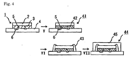
Fig. 4 , V to VII). When achip 2 is mounted on awiring board 4 via an uncuredadhesive layer 3,voids 5 are often formed in the adhesive, orvoids 6 may be produced in an interface between the adhesive and the chip or the wiring board (Fig. 4 ). Such voids do not disappear and remain after the die-bonding step (Fig. 4 ). In particular, the use of a liquid adhesive frequently results in voids in the adhesive, and the use of a film adhesive often results in voids in the interface due to insufficient adhesion and insufficient followability to unevenness of an adherend surface. - These voids can be an origin of package cracks in reliability evaluation of semiconductor devices, and therefore should be eliminated.
- To address this problem,
Patent Document 1 improves the followability to unevenness of a wiring board by reducing the viscosity of a liquid adhesive applied, or by reducing the elastic modulus of a film adhesive used in the die-bonding or optimizing die-bonding conditions. - Patent Document 1:
WO 05/004216 - Although the above method can decrease voids in liquid adhesives or films adhesive, reducing the viscosity or the elastic modulus is accompanied by a problem that the adhesive squeezes out to edges of a die-bonded chip. Because chips are getting thinner in recent years, the adhesive that has squeezed out curls up onto the circuit surface of the chip to contaminate wire pads and reduce the bond strength of wires.
- Particularly in the use of films adhesive, designs of wiring boards are also a factor that affects voids forming in the interfaces. With each change of designs of wiring boards, compositions of the adhesives have to be changed to control the viscosity or the elastic modulus, or die-bonding conditions have to be reviewed or optimized. Further, the films adhesive are difficult to handle. Because recent high-density wiring boards have great unevenness, it is considerably difficult to perform die-bonding while the unevenness completely burried without causing voids.
- It is an object of the invention to provide a process whereby semiconductor devices are easily manufactured without causing voids and, additionally, to provide a process whereby semiconductor devices are manufactured without causing voids and curling of an adhesive irrespective of the design of a wiring board.
- The present inventors have diligently studied and have found that the above problems are solved by performing a specific statically pressurizing step. The present invention has been completed based on the finding.
- In a process for manufacturing a semiconductor device comprising heating a wiring board on which a chip and an uncured adhesive layer are laminated (the chip is mounted via the uncured adhesive layer) for curing the adhesive layer, the improvement of the present invention comprises performing a statically pressurizing step before the adhesive layer is cured (the curing reaction has completed), in which step the wiring board on which the chip and the uncured adhesive layer are laminated is subjected to a static pressure greater than atmospheric pressure by not less than 0.05 MPa.
- In the process for manufacturing a semiconductor device, the improvement preferably comprises performing a heat curing step in which the wiring board on which the chip and the uncured adhesive layer are laminated is heated to cure the adhesive layer while maintaining the static pressure applied in the statically pressurizing step.
- According to the process for manufacturing a semiconductor device of the present invention, a chip is mounted on a wiring board via an uncured adhesive layer under usual conditions, and voids are easily eliminated in the subsequent statically pressurizing step irrespective of the design of the wiring board. Because the pressure applied to the wiring board in the statically pressurizing step is static, the adhesive does not curl up.
-
-
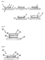
Fig. 1 is a drawing showing a process for manufacturing a semiconductor device according to the present invention; -
Fig. 2 shows an example of a wiring board used in the present invention in which chips and an uncured adhesive layer are laminated; -
Fig. 3 shows an example of a wiring board used in the present invention in which a chip and an uncured adhesive layer are laminated; and -
Fig. 4 is a drawing showing a conventional process for manufacturing a semiconductor device. -
- 1. Wiring board on which a chip and an uncured adhesive layer are laminated
- 2. Chip
- 3. Uncured adhesive layer
- 4. Wiring board
- 5. Void in the adhesive layer
- 6. Void in the interface between the wiring board and the adhesive layer
- 8. Cured adhesive layer
- 9. Wire
- 10. Semiconductor device
- 11. Encapsulating resin
- I. Statically pressurizing step
- II. Heat curing step
- III. Wire-bonding step
- IV. Encapsulating step
- 21. Multi-stack semiconductor device before encapsulation
- 22. Relatively upper (second layer) chip
- 23. Uncured adhesive layer
- 25. Relatively lower (first layer) chip (wiring board)
- 26. Adhesive layer
- 27. Wiring board for mounting a chip
- 31. Wiring board on which a chip and an uncured adhesive layer (underfill material) are laminated (the chip is flip chip bonded)
- 32. Chip
- 33. Uncured adhesive layer
- 34. Wiring board
- 35. Bump
- 41. Wiring board having a sufficiently cured adhesive layer
- 42. Cured adhesive layer
- 43. Wire
- 44. Semiconductor device
- 45. Encapsulating resin
- V. Die-bonding step
- VI. Wire-bonding step
- VII. Encapsulating step
- The present invention will be described below.
- In the process for manufacturing a semiconductor device according to the invention, a
wiring board 1 on which achip 2 and an uncuredadhesive layer 3 are laminated (awiring board 1 on which achip 2 is die-bonded through an uncuredadhesive layer 3, the same applies hereinafter) is heated to cure the uncuredadhesive layer 3. A semiconductor device is thus manufactured (Fig. 1 ). In the final semiconductor device, the adhesive layer is sufficiently cured. - The
chips 2 are obtained by cutting a semiconductor wafer with respect to respective circuits. Examples of thewiring boards 4 include lead frames of metals, boards of organic or inorganic materials, and laminates of metals and organic or inorganic materials. When a multi-stack semiconductor device is manufactured, a relatively lower chip is regarded as part of a wiring board. - The uncured
adhesive layer 3 is a film adhesive or a liquid adhesive, and is preferably a film adhesive. The adhesive used in the invention is a thermosetting adhesive which contains a thermosetting resin. Examples of the thermosetting resins include epoxy resins, phenoxy resins, phenol resins, resorcinol resins, urea resins, melamine resins, furane resins, unsaturated polyester resins and silicone resins. The thermosetting resin is used in combination with an appropriate curing agent and an optional curing accelerator. Conventional thermosetting resins may be used in the invention without limitation. The thermosetting adhesive may be a sticky adhesive that shows stickiness at ordinary temperature. The sticky adhesive used herein is an adhesive that shows stickiness at ordinary temperature in an initial state and shows strong adhesion when cured by a trigger such as heat. Examples of the sticky adhesives include mixtures of binder resins showing pressure sensitive adhesion at ordinary temperature and the above-mentioned thermosetting resins. Examples of the binder resins showing pressure sensitive adhesion at ordinary temperature include acrylic resins, polyester resins, polyvinyl ether resins, urethane resins and polyamide resins. - When the
adhesive layer 3 is a film adhesive, a dicing/die-bonding sheet having a film adhesive layer may be used. The dicing/die-bonding sheet includes a base film and a film adhesive layer of the above composition that is releasably laminated on the base film. The releasability of the film adhesive layer from the base film may be preferably controlled by incorporating an energy ray curable resin such as a urethane acrylate oligomer in the adhesive of the film adhesive layer. The adhesive containing the energy ray curable resin shows high adhesion to the base film before energy ray irradiation and is easily released from the base film after the energy ray irradiation. - The thickness of the film adhesive layer in the dicing/die-bonding sheet is variable depending on the level and shape of unevenness of a wiring board that is an adherend. The thickness is generally in the range of 3 to 100 µm, preferably 10 to 50 µm.
- When the
adhesive layer 3 is a liquid adhesive, the adhesive may be a liquid (paste) adhesive of the same composition as that of the above-mentioned film adhesive layer except for the binder resin. That is, the liquid (paste) adhesive may comprise the thermosetting resin and the curing agent. - The process of the present invention will be described with reference to an embodiment using a dicing/die-bonding sheet (film adhesive).
- In an embodiment using a dicing/die-bonding sheet, the process for manufacturing a semiconductor device includes (1) a dicing step (1), a die-bonding step (2), a statically pressurizing step (3), a heat curing step (4), and an assembling step (5).
- In the dicing step (1), a dicing/die-bonding sheet is applied to a wafer such as silicon, and the wafer and an uncured adhesive layer are diced. The resultant chips have the uncured adhesive layer on one surface. When the dicing/die-bonding sheet has energy ray curability, an energy ray may be applied before or after the dicing step to reduce the adhesion to a base film. Depending on conditions under which the dicing/die-bonding sheet is applied, voids may form in the interface between the chip and the uncured adhesive layer.
- In the die-bonding step (2), the chips are released (picked up) from the base film at the interface between the base film and the uncured
adhesive layer 3, and the chips having the uncured adhesive layer are mounted (die-bonded) on chip-mounting parts of a wiring board. Consequently, awiring board 1 is obtained on which thechips 2 are mounted through the uncuredadhesive layer 3. Depending on die-bonding conditions (such as pressure, temperature and time), voids 6 may form in the interface between the uncuredadhesive layer 3 and the wiring board 4 (Fig. 1 ). - In the statically pressurizing step (3), a pressure (static pressure) is uniformly applied in all directions to the wiring board on which the chips are die-bonded, before the uncured adhesive layer is sufficiently cured (
Fig. 1 , I). In the invention, the pressure is greater than atmospheric pressure by not less than 0.05 MPa, preferably by 0.1 to 1.0 MPa. That is, the pressure applied in the invention surpasses atmospheric pressure by not less than 0.05 MPa, preferably by 0.1 to 1.0 MPa. - According to an embodiment, the statically pressurizing step is performed as follows. The
wiring board 1 on which thechips 2 are die-bonded through the uncuredadhesive layer 3 is subjected to the static pressure (Fig. 1 , I). The application of the static pressure removes voids (not shown) between theadhesive layer 3 and thechip 2 orvoids 6 between theadhesive layer 3 and thewiring board 4. Even when thewiring board 4 has a fine circuit design with great unevenness, thevoids 6 that have occurred in the interface between theadhesive layer 3 and thewiring board 4 are eliminated by the statically pressurizing step. According to the invention, thevoids 6 are easily removed without controlling conditions under which thechips 2 are mounted on thewiring board 4 through the uncuredadhesive layer 3. The static pressure applied in the statically pressurizing step pressurizes the laminate uniformly in all directions and prevents the adhesive from squeezing out and curling up. - The pressure in the range as described above can efficiently eliminate the voids and can be applied by general-purpose pressurizing apparatuses and pressure-resistant explosion-proof equipment, enabling a compact production line. The pressure in the above range is also advantageous in that it can be reached immediately.
- The pressurizing time is preferably in the range of 1 to 120 minutes, more preferably 5 to 90 minutes.
- The statically pressurizing apparatus used in the invention is not particularly limited as long as it can apply a static pressure to the
wiring board 1 on which the chips are die-bonded. Preferred examples of the pressurizing apparatuses include autoclaves (pressure tight cases with a compressor). Increasing the pressure in an autoclave having a fixed volume results in an elevated temperature of the atmosphere. Because the temperature is preferably constant for stable production of semiconductor devices, the temperature may be controlled while avoiding the curing of theadhesive layer 3. At controlled high temperatures, the adhesive layer is fluidized to permit the voids to move easily, and the voids may be eliminated easily. The temperature may be controlled appropriately depending on the composition of the adhesive of theadhesive layer 3, and is for example in the range of about 30 to 120°C. - In the heat curing step (4), the uncured
adhesive layer 3 of thewiring board 1 is sufficiently cured by heating (Fig. 1 , II). As used herein, the term "uncured" means that curing reaction has not proceeded in the adhesive, and the term "sufficiently cured" means that the curing reaction has completed and the adhesive is not deformed. Thewiring board 1 from which the voids are eliminated in the statically pressurizing step (3) is removed from the pressurizing apparatus and is introduced into a heating apparatus in which the pressure is atmospheric. The uncuredadhesive layer 3 is cured to give a curedadhesive layer 8, which shows bonding performance required as a die-bonding adhesive in the semiconductor device. This wiring board maintains a state created in the statically pressurizing step (3). That is, no voids are in the interfaces on both sides of theadhesive layer 8, and thechips 2 and thewiring board 4 are firmly bonded. - The heating temperature and time are not particularly limited as long as the adhesive layer is sufficiently cured. These conditions are dependent on the composition of the adhesive. The heating temperature is preferably in the range of 100 to 200°C, more preferably 120 to 160°C, and the heating time is preferably in the range of 15 to 300 minutes, more preferably 30 to 180 minutes.
- The heating apparatus for the heat curing is not particularly limited, and may be a conventional heat curing apparatus (such as an oven).
- In the assembling step (5), the chips of the wiring board having the cured adhesive layer are assembled into semiconductor devices. For example, referring to
Fig. 1 , wires 9 are connected (wire-bonding step) and the chips are encapsulated with an encapsulating resin 11 (encapsulating step) (Fig. 1 , III and IV).Semiconductor devices 10 are thus manufactured. Thesemiconductor devices 10 obtained by the process of the invention have no voids in the interfaces of the adhesive layer and are not cracked in reliability evaluation. - In the above-described embodiment, the heat curing step (4) is performed at atmospheric pressure after the statically pressurizing step (3). It is also within the scope of the invention to cure the uncured
adhesive layer 3 by heating at static pressure in the statically pressurizing step (3). - Specifically, in such an embodiment, the statically pressurizing step is performed to eliminate the voids and the heat curing step is simultaneously carried out at the static pressure to sufficiently cure the
adhesive layer 3, and the statically pressurizing step and the heat curing step are terminated at the same time. In this embodiment, the heat curing at a high temperature may cause voids in the adhesive layer, but such voids are eliminated by the static pressure immediately after they are formed. In the final semiconductor devices, no voids are within and on the boundaries of the adhesive layer, and the adhesive layer is sufficiently cured and firmly bonds the chip and the wiring board. - In this embodiment, the pressure is greater than atmospheric pressure by not less than 0.05 MPa, preferably by 0.1 to 1.0 MPa. The heating temperature is not particularly limited as long as the adhesive layer is sufficiently cured, and is preferably in the range of 100 to 200°C, more preferably 120 to 160°C.
- The pressurizing time and the heating time are not particularly limited as long as the voids are eliminated and the adhesive layer is sufficiently cured, and are preferably in the range of 15 to 300 minutes, more preferably 30 to 180 minutes.
- According to an embodiment of the invention, the heat curing step may be performed in two stages in which the first stage is carried out under heating conditions such that the adhesive layer is not cured, and the second stage is carried out under heating conditions such that the adhesive layer is cured. The heating conditions in the first stage may be such that the heating temperature is about 30 to 120°C and the heating time is preferably 1 to 120 minutes, more preferably 5 to 90 minutes. The heating conditions in the second stage may be such that the heating temperature is 120 to 200°C and the heating time is preferably 15 to 300 minutes, more preferably 30 to 180 minutes.
- In the process for manufacturing semiconductor devices of the present invention, the
adhesive layer 3 may be formed of a liquid (paste) adhesive. When a liquid adhesive is used, chips are prepared by cutting a wafer in the dicing step (1) using a general dicing sheet without a die-bonding function, instead of the dicing/die-bonding sheet. In the die-bonding step (2), the chips are picked up and are die-bonded to a wiring board coated with a liquid adhesive. The statically pressurizing step (3), the heat curing step (4) and the assembling step (5) may be performed as described hereinabove. To improve handling properties of the wiring board on which the chips are die-bonded, the liquid adhesive may be semi-cured (B-staged) by heating before the statically pressurizing step (3). Even ifvoids 5 form in the liquidadhesive layer 3 in the die-bonding step, they are eliminated in the statically pressurizing step (Fig. 4 ). - Configurations of the semiconductor devices manufactured by the process of the invention are not limited to the aforesaid embodiments, and the process of the invention may be applied to production of semiconductor devices having various structures.
- For example, the process of the invention may be applied to production of multi-stack semiconductor devices. Specifically, the process may be used for die-bonding a relatively
upper chip 22 and a relatively lower chip 25 (wiring board) to which wires may be connected, through an uncured adhesive layer 23 (Fig. 2 ). Obtainable semiconductor devices may be same-size stack semiconductor devices in which the upper and lower chips have a same size as shown inFig. 2 , or may be pyramid multi-stack semiconductor devices in which the chips are of different sizes. The same-size stack semiconductor devices may be such that connected wires are buried in theadhesive layer 23, in which case the present invention is advantageous because voids around the wires are eliminated. - The multi-stack semiconductor devices may be manufactured according to the aforesaid embodiments except that the
lower chip 25 is used as a substitute for thewiring board 1. - The process of the invention may be used for manufacturing flip chip semiconductor devices as shown in
Fig. 3 . In this case, an underfill material used in the flip chip bonding corresponds to the uncured adhesive layer. The underfill material may be a liquid (paste) or a sheet. A heat curable underfill sheet described in Japanese Patent Application No.2005-129502 - The following is an embodiment of the process using an underfill sheet. A semiconductor wafer is prepared in which bumps are formed on a circuit surface. An underfill layer (adhesive layer 33) of an underfill sheet is attached to the circuit surface of the semiconductor wafer such that the bumps penetrate the underfill layer. A general dicing tape is attached to the back surface of the semiconductor wafer, and the wafer is fixed to a ring frame via the dicing tape. The semiconductor wafer is cut into chips with a dicing apparatus. The base of the underfill sheet is removed to expose the tops of the bumps. In the consequent chip, the circuit surface is covered with the
uncured adhesive layer 33, and the tops of thebumps 35 are exposed from theadhesive layer 33. Thechip 32 is mounted on awiring board 34 with alignment such that thebumps 35 are opposed to electrodes of thewiring board 34 to establish electrical conduction between thechip 32 and thewiring board 34. Awiring board 31 is thus prepared in which the chips are mounted (flip chip bonded) through the uncured adhesive layer 33 (underfill material). - In this embodiment, the wiring board on which the chips are flip chip bonded is subjected to the statically pressurizing step (3), the heat curing step (4) and the assembling step (5) as described hereinabove. In this embodiment, the wire-bonding step in the assembling step (5) is not necessary. The uncured adhesive layer 33 (underfill material) is cured and the chips are encapsulated. Semiconductor devices are thus manufactured.
- The present invention will be described by Examples below without limiting the scope of the invention.
- A dicing/die-bonding sheet (Adwill LE-5003, manufactured by LINTEC Corporation) was attached to a dummy silicon wafer (200 mm in diameter, 150 µm in thickness) with use of a tape mounter (Adwill RAD 2500 m/8, manufactured by LINTEC Corporation). The wafer was fixed to a ring frame at the same time. The dicing/die-bonding sheet was UV irradiated through a base film thereof using a UV irradiator (Adwill RAD 2000 m/8, manufactured by LINTEC Corporation). The wafer was diced into 8 mm square chips with a dicing apparatus (DFD 651, manufactured by DISCO Corporation). The cutting depth was such that the base film of the dicing/die-bonding sheet was cut to a depth of 20 µm.
- A wiring board (manufactured by CHINO GIKEN Co., Ltd.) used for die-bonding the chips was a copper-clad laminate (CCL-HL830, manufactured by MITSUBISHI GAS CHEMICAL COMPANY, INC.) in which the copper foil formed circuit patterns and a solder resist (PSR-4000 AUS5, manufactured by TAIYO INK MFG. CO. , LTD.) was on the respective patterns. The silicon chips obtained in the step (1) were picked up together with the sticky adhesive layer (uncured adhesive layer) and were mounted on the wiring board via the sticky adhesive layer. The chips were compression bonded (die-bonded) at 100°C and 300 gf for 1 second.
- The wiring board on which the chips were die-bonded in the step (2) was placed in a heating pressurizer (autoclave manufactured by Kurihara Manufactory Inc.). The wiring board was heated at 100°C and a static pressure greater than atmospheric pressure by 0.5 MPa for 30 minutes. Voids in the sticky adhesive layer were thus eliminated.
- The wiring board was removed from the heating pressurizer and was introduced into an oven. The wiring board was heated at 120°C and atmospheric pressure for 1 hour, and subsequently at 140°C and atmospheric pressure for 1 hour. The sticky adhesive layer was thus cured.
- The chips on the wiring board obtained in the step (3) were encapsulated with an encapsulating resin (KE-1100 AS3, manufactured by KYOCERA Chemical Corporation) in an encapsulating thickness of 400 µm by use of an encapsulating apparatus (MPC-06M Trial Press, manufactured by APIC YAMADA CORPORATION). The encapsulating resin was cured at 175°C in 5 hours. The encapsulated wiring board was attached to a dicing tape (Adwill D-510T, manufactured by LINTEC Corporation) and the encapsulated wiring board was cut into 12 mm squares with use of a dicing apparatus (DFD 651, manufactured by DISCO Corporation). Consequently, simulated wire-free semiconductor devices having the dummy chips were manufactured.
- Simulated semiconductor devices were manufactured in the same manner as in Example 1, except that the statically pressurizing step (3) was carried out under the conditions shown in Table 1. In Table 1, the pressure is expressed by a value by which the pressure surpassed atmospheric pressure.
-
[Table 1] Pressure (MPa) Temperature (°C) Time (minutes) Ex. 1 0.5 100 30 Ex. 2 0.1 100 30 Ex. 3 0.9 100 30 Ex. 4 0.5 50 30 Ex. 5 0.5 100 10 Ex. 6 0.5 100 60 - Simulated semiconductor devices were manufactured in the same manner as in Example 1, except that the statically pressurizing step (3) and the heat curing step (4) were started and completed simultaneously. Specifically, the sticky adhesive layer was sufficiently cured at a static pressure greater than atmospheric pressure by 0.5 MPa, at 120°C for 1 hour and then at 140°C for 1 hour.
- Simulated semiconductor devices were manufactured in the same manner as in Example 1, except that the dicing/die-bonding sheet was changed to Adwill LE-5006 (manufactured by LINTEC Corporation).
- A UV-curable dicing tape (Adwill D-628, manufactured by LINTEC Corporation) was attached to a dummy silicon wafer (200 mm in diameter, 150 µm in thickness) with use of a tape mounter (Adwill RAD 2500 m/8, manufactured by LINTEC Corporation). The wafer was fixed to a ring frame at the same time. The wafer was diced into 8 mm square chips with a dicing apparatus (DFD 651, manufactured by DISCO Corporation). The cutting depth was such that a base film of the dicing tape was cut to a depth of 20 µm. The dicing tape was UV irradiated through the base film thereof using a UV irradiator (Adwill RAD 2000 m/8, manufactured by LINTEC Corporation).
- A wiring board (manufactured by CHINO GIKEN Co., Ltd.) used for die-bonding the chips was a copper-clad laminate (CCL-HL830, manufactured by MITSUBISHI GAS CHEMICAL COMPANY, INC.) in which the copper foil formed circuit patterns and a solder resist (PSR-4000 AUS5, manufactured by TAIYO INK MFG. CO., LTD.) was on the respective patterns. A paste adhesive of the following composition was applied to the wiring board. The silicon chips obtained in the step (1) were picked up and were placed on the paste adhesive on the respective wiring patterns. The chips were compression bonded (die-bonded) at 23°C and 100 gf for 1 second.
-
- 30 parts by weight of a liquid bisphenol A-skeleton epoxy resin (EPIKOTE 828, manufactured by Japan Epoxy Resins Co., Ltd.)
- 15 parts by weight of a glycidylamine epoxy resin (EPIKOTE 630, manufactured by Japan Epoxy Resins Co., Ltd.)
- 5 parts by weight of a novolak epoxy resin (EOCN-102S, manufactured by NIPPON KAYAKU CO., LTD.)
- 5 parts by weight of a dispersion of a curing agent (ADEKA HARDENER 3636AS, manufactured by ADEKA CORPORATION) in an organic solvent (methyl ethyl ketone) (solid concentration: 15%)
- 10 parts by weight of a dispersion of a curing accelerator (CUREZOL 2PHZ, manufactured by SHIKOKU CHEMICALS CORPORATION) in an organic solvent (methyl ethyl ketone) (solid concentration: 15%)
- A statically pressurizing step (3) and a heat curing step (4) were started and completed simultaneously. Specifically, the wiring board on which the chips were die-bonded was placed in a heating pressurizer (autoclave manufactured by Kurihara Manufactory Inc.). The adhesive layer was cured at a static pressure greater than atmospheric pressure by 0.5 MPa, at 120°C for 1 hour and then at 140°C for 1 hour.
- The chips on the wiring board obtained in the step (3) were encapsulated with an encapsulating resin (KE-1100 AS3, manufactured by KYOCERA Chemical Corporation) in an encapsulating thickness of 400 µm by use of an encapsulating apparatus (MPC-06M Trial Press, manufactured by APIC YAMADA CORPORATION). The encapsulating resin was cured at 175°C in 5 hours. The encapsulated wiring board was attached to a dicing tape (Adwill D-510T, manufactured by LINTEC Corporation) and the encapsulated wiring board was cut into 12 mm squares with use of a dicing apparatus (DFD 651, manufactured by DISCO Corporation). Simulated semiconductor devices were thus manufactured.
- Simulated semiconductor devices were manufactured in the same manner as in Example 1, except that the wiring board on which chips were die-bonded was placed in the heating pressurizer but was not pressurized, and the sticky adhesive layer was cured in the pressurizer by heating at 120°C and atmospheric pressure for 1 hour, and subsequently at 140°C and atmospheric pressure for 1 hour. In this Comparative Example, the statically pressurizing step was not performed.
- Example 9 was reproduced except that the chips were compression bonded at 23°C and 500 gf for 1 second in the die-bonding step (2). The die-bonding step resulted in the excessive curling up of the adhesive and the subsequent steps were cancelled.
- Examples and Comparative Examples were reproduced except that the silicon wafer was replaced by a transparent glass circular plate (manufactured by NSG PRECISION Co., Ltd., 8 inch in diameter, 100 µm in thickness). The wiring board on which the glass chips were die-bonded displayed the adhesive layer through the transparent glass chips, and the board was inspected for voids with a digital microscope. The results are shown in Table 2.
- At the completion of the statically pressurizing step (3) and the heat curing step (4) in each of Examples and Comparative Examples, the cross section of the wiring board on which the chips were die-bonded and the surface of the chips were observed with a digital microscope to determine whether the adhesive curled up on the chip surface. The results are shown in Table 2.
- The semiconductor devices (semiconductor packages) obtained in the encapsulating step (5) in each of Examples and Comparative Examples were allowed to stand at 85°C and 60% RH for 168 hours and thereby were allowed to absorb moisture. The packages were then subjected to IR reflow conditions at a maximum temperature of 260°C for a heating time of 1 minute (reflow furnace: WL-15-20DNX, manufactured by Sagami-Rikou Co., Ltd.). These moisture absorption and heating treatments were repeated three times. The packages were cross sectionally observed with a scanning ultrasonic flaw detector (Hye-Focus, manufactured by Hitachi Kenki Fine Tech Co., Ltd.) to determine whether lifting or separation occurred in the joints of the chip and the wiring board and whether the packages were cracked. When the joints were separated by a length of 0.5 mm or more, the semiconductor packages were rejected. Twenty five semiconductor packages were tested, and the packages without such separation were counted. The results are shown in Table 2.
-
[Table 2] Voids Curling of adhesive Package reliability After step (2) After step (3) After step (4) After step (2) After step (3) After step (4) Ex. 1 Present Not present Not present Not present Not present Not present 25/25 Ex. 2 Present Not present Not present Not present Not present Not present 25/25 Ex. 3 Present Not present Not present Not present Not present Not present 25/25 Ex. 4 Present Not present Not present Not present Not present Not present 25/25 Ex. 5 Present Not present Not present Not present Not present Not present 25/25 Ex. 6 Present Not present Not present Not present Not present Not present 25/25 Ex. 7 Present Not present Not present Not present 25/25 Ex. 8 Present Not present Not present Not present Not present Not present 25/25 Ex. 9 Present Not present Not present Not present 25/25 Comp. Ex. 1 Present - Present Not present - Not present 10/25 Comp. Ex. 2 Not present - - Present - - -
Claims (2)
- In a process for manufacturing a semiconductor device comprising heating a wiring board on which a chip and an uncured adhesive layer are laminated for curing the adhesive layer, the improvement comprising performing a statically pressurizing step before the adhesive layer is cured, in which step the wiring board on which the chip and the uncured adhesive layer are laminated is subjected to a static pressure greater than atmospheric pressure by not less than 0.05 MPa.
- In the process for manufacturing a semiconductor device according to claim 1, the improvement comprising performing a heat curing step in which the wiring board on which the chip and the uncured adhesive layer are laminated is heated to cure the adhesive layer while maintaining the static pressure applied in the statically pressurizing step.
Applications Claiming Priority (2)
| Application Number | Priority Date | Filing Date | Title |
|---|---|---|---|
| JP2006251131 | 2006-09-15 | ||
| PCT/JP2007/065418 WO2008032510A1 (en) | 2006-09-15 | 2007-08-07 | Process for producing semiconductor device |
Publications (2)
| Publication Number | Publication Date |
|---|---|
| EP2063465A1 true EP2063465A1 (en) | 2009-05-27 |
| EP2063465A4 EP2063465A4 (en) | 2012-08-08 |
Family
ID=39183576
Family Applications (1)
| Application Number | Title | Priority Date | Filing Date |
|---|---|---|---|
| EP07792087A Withdrawn EP2063465A4 (en) | 2006-09-15 | 2007-08-07 | METHOD FOR PRODUCING SEMICONDUCTOR DEVICE |
Country Status (7)
| Country | Link |
|---|---|
| US (1) | US8545663B2 (en) |
| EP (1) | EP2063465A4 (en) |
| KR (2) | KR20090053954A (en) |
| CN (1) | CN101517720A (en) |
| MY (1) | MY153208A (en) |
| TW (1) | TWI415198B (en) |
| WO (1) | WO2008032510A1 (en) |
Families Citing this family (5)
| Publication number | Priority date | Publication date | Assignee | Title |
|---|---|---|---|---|
| JP2010245412A (en) * | 2009-04-09 | 2010-10-28 | Renesas Electronics Corp | Manufacturing method of semiconductor integrated circuit device |
| US9079351B2 (en) * | 2012-06-22 | 2015-07-14 | Wisconsin Alumni Research Foundation | System for transfer of nanomembrane elements with improved preservation of spatial integrity |
| KR101696539B1 (en) * | 2015-03-09 | 2017-01-16 | 한양대학교 산학협력단 | Thin film, method of fabricating the same, apparatus for fabricating the same |
| JP6661847B1 (en) * | 2018-03-29 | 2020-03-11 | リンテック株式会社 | Method for joining two adherends and method for manufacturing joined structure |
| KR102555721B1 (en) * | 2018-08-20 | 2023-07-17 | 삼성전자주식회사 | method for bonding flip chip |
Family Cites Families (24)
| Publication number | Priority date | Publication date | Assignee | Title |
|---|---|---|---|---|
| JPH03169029A (en) | 1989-11-28 | 1991-07-22 | Mitsubishi Electric Corp | Mounting of semiconductor device |
| US5853651A (en) * | 1995-09-07 | 1998-12-29 | Simula, Inc. | High pressure hollow process for manufacturing composite structures |
| JP4032317B2 (en) * | 1996-08-06 | 2008-01-16 | 日立化成工業株式会社 | Chip mounting method |
| JP3928753B2 (en) * | 1996-08-06 | 2007-06-13 | 日立化成工業株式会社 | Multi-chip mounting method and manufacturing method of chip with adhesive |
| JP3053839U (en) | 1998-05-07 | 1998-11-17 | 中央電子株式会社 | Sliding equipment installation table |
| JP2000114204A (en) | 1998-10-01 | 2000-04-21 | Mitsubishi Electric Corp | Wafer sheet, method of manufacturing semiconductor device using the same, and semiconductor manufacturing apparatus |
| JP2001230528A (en) * | 2000-02-15 | 2001-08-24 | Sony Corp | Mounting device and mounting method |
| US6513236B2 (en) * | 2000-02-18 | 2003-02-04 | Matsushita Electric Industrial Co., Ltd. | Method of manufacturing bump-component mounted body and device for manufacturing the same |
| US6524891B1 (en) * | 2000-02-29 | 2003-02-25 | Micron Technology, Inc. | Method of pressure curing for reducing voids in a die attach bondline and applications thereof |
| DE10019443A1 (en) * | 2000-04-19 | 2001-10-31 | Texas Instruments Deutschland | Device for fastening a semiconductor chip on a chip carrier |
| JP3906962B2 (en) * | 2000-08-31 | 2007-04-18 | リンテック株式会社 | Manufacturing method of semiconductor device |
| JP4513235B2 (en) * | 2001-05-31 | 2010-07-28 | ソニー株式会社 | Flip chip mounting device |
| TW536768B (en) * | 2001-08-03 | 2003-06-11 | Matsushita Electric Industrial Co Ltd | Method for fabricating semiconductor-mounting body and apparatus for fabricating semiconductor-mounting body |
| JP4710205B2 (en) * | 2001-09-06 | 2011-06-29 | ソニー株式会社 | Flip chip mounting method |
| US20040238115A1 (en) * | 2001-09-12 | 2004-12-02 | Hisao Matsuno | Circuit device mounting method and press |
| JP2004311709A (en) * | 2003-04-07 | 2004-11-04 | Renesas Technology Corp | Semiconductor device manufacturing method and semiconductor manufacturing apparatus |
| EP1650790B1 (en) | 2003-07-08 | 2010-04-28 | LINTEC Corporation | Hardenable pressure sensitive adhesive sheet for dicing/die-bonding and method for manufacturing semiconductor device |
| JP3921459B2 (en) * | 2003-07-11 | 2007-05-30 | ソニーケミカル&インフォメーションデバイス株式会社 | Mounting method and mounting apparatus for electrical parts |
| JP2004031975A (en) * | 2003-07-22 | 2004-01-29 | Hitachi Chem Co Ltd | Connection device |
| JP2005129502A (en) | 2003-09-29 | 2005-05-19 | Pioneer Plasma Display Corp | Plasma display panel and plasma display device |
| US20050208700A1 (en) * | 2004-03-19 | 2005-09-22 | Chippac, Inc. | Die to substrate attach using printed adhesive |
| US20060252234A1 (en) | 2004-07-07 | 2006-11-09 | Lintec Corporation | Hardenable pressure sensitive adhesive sheet for dicing/die-bonding and method for manufacturing semiconductor device |
| JP2008159819A (en) | 2006-12-22 | 2008-07-10 | Tdk Corp | Electronic component mounting method, electronic component embedded substrate manufacturing method, and electronic component embedded substrate |
| JP2008159820A (en) * | 2006-12-22 | 2008-07-10 | Tdk Corp | Electronic component batch mounting method and electronic component built-in substrate manufacturing method |
-
2007
- 2007-08-07 CN CNA2007800342350A patent/CN101517720A/en active Pending
- 2007-08-07 MY MYPI20090907A patent/MY153208A/en unknown
- 2007-08-07 EP EP07792087A patent/EP2063465A4/en not_active Withdrawn
- 2007-08-07 WO PCT/JP2007/065418 patent/WO2008032510A1/en not_active Ceased
- 2007-08-07 KR KR1020097007517A patent/KR20090053954A/en not_active Ceased
- 2007-08-07 KR KR1020117025251A patent/KR101299773B1/en active Active
- 2007-08-08 US US11/835,606 patent/US8545663B2/en not_active Expired - Fee Related
- 2007-08-16 TW TW096130285A patent/TWI415198B/en active
Also Published As
| Publication number | Publication date |
|---|---|
| CN101517720A (en) | 2009-08-26 |
| TW200818347A (en) | 2008-04-16 |
| KR20090053954A (en) | 2009-05-28 |
| US8545663B2 (en) | 2013-10-01 |
| US20080066856A1 (en) | 2008-03-20 |
| WO2008032510A1 (en) | 2008-03-20 |
| TWI415198B (en) | 2013-11-11 |
| MY153208A (en) | 2015-01-29 |
| KR101299773B1 (en) | 2013-08-23 |
| EP2063465A4 (en) | 2012-08-08 |
| KR20110131313A (en) | 2011-12-06 |
Similar Documents
| Publication | Publication Date | Title |
|---|---|---|
| US6911720B2 (en) | Semiconductor device adhesive sheet with conductor bodies buried therein | |
| JP4409014B2 (en) | Manufacturing method of semiconductor device | |
| KR101276487B1 (en) | Wafer laminated body and method for bonding and debonding between device wafer and carrier wafer | |
| JP5477144B2 (en) | Adhesive sheet for connecting circuit members and method for manufacturing semiconductor device | |
| KR20140140042A (en) | Method and apparatus for manufacturing semiconductor device | |
| KR20120104109A (en) | Die-bonding film and use thereof | |
| JP2009027054A (en) | Manufacturing method of semiconductor device | |
| JP4766200B2 (en) | Adhesive composition and method for manufacturing semiconductor device | |
| CN100423201C (en) | Adhesive sheet for dicing and/or die bonding and method for manufacturing semiconductor device | |
| KR101799499B1 (en) | Adhesive composition for semiconductor, adhesive film, dicing die bonding film, and semiconductor device | |
| JP5515811B2 (en) | Manufacturing method of semiconductor device and adhesive sheet for connecting circuit member | |
| US8545663B2 (en) | Process for manufacturing semiconductor devices | |
| JP5219302B2 (en) | Thermosetting die bond film, dicing die bond film, and semiconductor device | |
| JP5224710B2 (en) | Adhesive used in semiconductor device manufacturing method | |
| WO2020100998A1 (en) | Semiconductor device and manufacturing method thereof, and structure used in manufacture of semiconductor device | |
| US11084941B2 (en) | Underfill material, underfill film, and method for manufacturing semiconductor device using same | |
| TWI425066B (en) | Preparation method of adhesive composition, circuit board for connecting circuit member, and manufacturing method of semiconductor device | |
| JP2008098608A (en) | Manufacturing method of semiconductor device | |
| JP2012216651A (en) | Semiconductor device | |
| JP5406995B2 (en) | Adhesive used in semiconductor device manufacturing method | |
| JP5270191B2 (en) | Manufacturing method of semiconductor device | |
| JP6690308B2 (en) | Method for manufacturing semiconductor device | |
| JP2011114301A (en) | Manufacturing method for semiconductor device | |
| KR20250078374A (en) | Manufacturing method of semiconductor device and adhesive film for semiconductor wafer processing | |
| KR20250078375A (en) | Manufacturing method of semiconductor device and adhesive film for semiconductor wafer processing |
Legal Events
| Date | Code | Title | Description |
|---|---|---|---|
| PUAI | Public reference made under article 153(3) epc to a published international application that has entered the european phase |
Free format text: ORIGINAL CODE: 0009012 |
|
| 17P | Request for examination filed |
Effective date: 20090313 |
|
| AK | Designated contracting states |
Kind code of ref document: A1 Designated state(s): AT BE BG CH CY CZ DE DK EE ES FI FR GB GR HU IE IS IT LI LT LU LV MC MT NL PL PT RO SE SI SK TR |
|
| AX | Request for extension of the european patent |
Extension state: AL BA HR MK RS |
|
| DAX | Request for extension of the european patent (deleted) | ||
| RBV | Designated contracting states (corrected) |
Designated state(s): DE PT |
|
| RIC1 | Information provided on ipc code assigned before grant |
Ipc: H01L 21/58 20060101ALI20120618BHEP Ipc: H01L 21/60 20060101ALI20120618BHEP Ipc: H01L 21/683 20060101ALI20120618BHEP Ipc: H01L 21/52 20060101AFI20120618BHEP Ipc: H01L 21/00 20060101ALI20120618BHEP |
|
| A4 | Supplementary search report drawn up and despatched |
Effective date: 20120706 |
|
| RIC1 | Information provided on ipc code assigned before grant |
Ipc: H01L 21/52 20060101AFI20120702BHEP Ipc: H01L 21/683 20060101ALI20120702BHEP Ipc: H01L 21/58 20060101ALI20120702BHEP Ipc: H01L 21/60 20060101ALI20120702BHEP Ipc: H01L 21/00 20060101ALI20120702BHEP |
|
| STAA | Information on the status of an ep patent application or granted ep patent |
Free format text: STATUS: THE APPLICATION IS DEEMED TO BE WITHDRAWN |
|
| 18D | Application deemed to be withdrawn |
Effective date: 20130205 |