EP2058845A1 - Thin film manufacturing apparatus using discharge electrode, and solar cell manufacturing method - Google Patents
Thin film manufacturing apparatus using discharge electrode, and solar cell manufacturing method Download PDFInfo
- Publication number
- EP2058845A1 EP2058845A1 EP07792889A EP07792889A EP2058845A1 EP 2058845 A1 EP2058845 A1 EP 2058845A1 EP 07792889 A EP07792889 A EP 07792889A EP 07792889 A EP07792889 A EP 07792889A EP 2058845 A1 EP2058845 A1 EP 2058845A1
- Authority
- EP
- European Patent Office
- Prior art keywords
- gas
- pipe
- electrode
- discharge electrode
- section
- Prior art date
- Legal status (The legal status is an assumption and is not a legal conclusion. Google has not performed a legal analysis and makes no representation as to the accuracy of the status listed.)
- Withdrawn
Links
Images





Classifications
-
- C—CHEMISTRY; METALLURGY
- C23—COATING METALLIC MATERIAL; COATING MATERIAL WITH METALLIC MATERIAL; CHEMICAL SURFACE TREATMENT; DIFFUSION TREATMENT OF METALLIC MATERIAL; COATING BY VACUUM EVAPORATION, BY SPUTTERING, BY ION IMPLANTATION OR BY CHEMICAL VAPOUR DEPOSITION, IN GENERAL; INHIBITING CORROSION OF METALLIC MATERIAL OR INCRUSTATION IN GENERAL
- C23C—COATING METALLIC MATERIAL; COATING MATERIAL WITH METALLIC MATERIAL; SURFACE TREATMENT OF METALLIC MATERIAL BY DIFFUSION INTO THE SURFACE, BY CHEMICAL CONVERSION OR SUBSTITUTION; COATING BY VACUUM EVAPORATION, BY SPUTTERING, BY ION IMPLANTATION OR BY CHEMICAL VAPOUR DEPOSITION, IN GENERAL
- C23C16/00—Chemical coating by decomposition of gaseous compounds, without leaving reaction products of surface material in the coating, i.e. chemical vapour deposition [CVD] processes
- C23C16/44—Chemical coating by decomposition of gaseous compounds, without leaving reaction products of surface material in the coating, i.e. chemical vapour deposition [CVD] processes characterised by the method of coating
- C23C16/50—Chemical coating by decomposition of gaseous compounds, without leaving reaction products of surface material in the coating, i.e. chemical vapour deposition [CVD] processes characterised by the method of coating using electric discharges
- C23C16/505—Chemical coating by decomposition of gaseous compounds, without leaving reaction products of surface material in the coating, i.e. chemical vapour deposition [CVD] processes characterised by the method of coating using electric discharges using radio frequency discharges
- C23C16/509—Chemical coating by decomposition of gaseous compounds, without leaving reaction products of surface material in the coating, i.e. chemical vapour deposition [CVD] processes characterised by the method of coating using electric discharges using radio frequency discharges using internal electrodes
-
- H—ELECTRICITY
- H01—ELECTRIC ELEMENTS
- H01G—CAPACITORS; CAPACITORS, RECTIFIERS, DETECTORS, SWITCHING DEVICES, LIGHT-SENSITIVE OR TEMPERATURE-SENSITIVE DEVICES OF THE ELECTROLYTIC TYPE
- H01G2/00—Details of capacitors not covered by a single one of groups H01G4/00-H01G11/00
- H01G2/20—Arrangements for preventing discharge from edges of electrodes
-
- C—CHEMISTRY; METALLURGY
- C23—COATING METALLIC MATERIAL; COATING MATERIAL WITH METALLIC MATERIAL; CHEMICAL SURFACE TREATMENT; DIFFUSION TREATMENT OF METALLIC MATERIAL; COATING BY VACUUM EVAPORATION, BY SPUTTERING, BY ION IMPLANTATION OR BY CHEMICAL VAPOUR DEPOSITION, IN GENERAL; INHIBITING CORROSION OF METALLIC MATERIAL OR INCRUSTATION IN GENERAL
- C23C—COATING METALLIC MATERIAL; COATING MATERIAL WITH METALLIC MATERIAL; SURFACE TREATMENT OF METALLIC MATERIAL BY DIFFUSION INTO THE SURFACE, BY CHEMICAL CONVERSION OR SUBSTITUTION; COATING BY VACUUM EVAPORATION, BY SPUTTERING, BY ION IMPLANTATION OR BY CHEMICAL VAPOUR DEPOSITION, IN GENERAL
- C23C16/00—Chemical coating by decomposition of gaseous compounds, without leaving reaction products of surface material in the coating, i.e. chemical vapour deposition [CVD] processes
- C23C16/44—Chemical coating by decomposition of gaseous compounds, without leaving reaction products of surface material in the coating, i.e. chemical vapour deposition [CVD] processes characterised by the method of coating
- C23C16/455—Chemical coating by decomposition of gaseous compounds, without leaving reaction products of surface material in the coating, i.e. chemical vapour deposition [CVD] processes characterised by the method of coating characterised by the method used for introducing gases into reaction chamber or for modifying gas flows in reaction chamber
- C23C16/45563—Gas nozzles
-
- C—CHEMISTRY; METALLURGY
- C23—COATING METALLIC MATERIAL; COATING MATERIAL WITH METALLIC MATERIAL; CHEMICAL SURFACE TREATMENT; DIFFUSION TREATMENT OF METALLIC MATERIAL; COATING BY VACUUM EVAPORATION, BY SPUTTERING, BY ION IMPLANTATION OR BY CHEMICAL VAPOUR DEPOSITION, IN GENERAL; INHIBITING CORROSION OF METALLIC MATERIAL OR INCRUSTATION IN GENERAL
- C23C—COATING METALLIC MATERIAL; COATING MATERIAL WITH METALLIC MATERIAL; SURFACE TREATMENT OF METALLIC MATERIAL BY DIFFUSION INTO THE SURFACE, BY CHEMICAL CONVERSION OR SUBSTITUTION; COATING BY VACUUM EVAPORATION, BY SPUTTERING, BY ION IMPLANTATION OR BY CHEMICAL VAPOUR DEPOSITION, IN GENERAL
- C23C16/00—Chemical coating by decomposition of gaseous compounds, without leaving reaction products of surface material in the coating, i.e. chemical vapour deposition [CVD] processes
- C23C16/44—Chemical coating by decomposition of gaseous compounds, without leaving reaction products of surface material in the coating, i.e. chemical vapour deposition [CVD] processes characterised by the method of coating
- C23C16/455—Chemical coating by decomposition of gaseous compounds, without leaving reaction products of surface material in the coating, i.e. chemical vapour deposition [CVD] processes characterised by the method of coating characterised by the method used for introducing gases into reaction chamber or for modifying gas flows in reaction chamber
- C23C16/45563—Gas nozzles
- C23C16/4557—Heated nozzles
-
- C—CHEMISTRY; METALLURGY
- C23—COATING METALLIC MATERIAL; COATING MATERIAL WITH METALLIC MATERIAL; CHEMICAL SURFACE TREATMENT; DIFFUSION TREATMENT OF METALLIC MATERIAL; COATING BY VACUUM EVAPORATION, BY SPUTTERING, BY ION IMPLANTATION OR BY CHEMICAL VAPOUR DEPOSITION, IN GENERAL; INHIBITING CORROSION OF METALLIC MATERIAL OR INCRUSTATION IN GENERAL
- C23C—COATING METALLIC MATERIAL; COATING MATERIAL WITH METALLIC MATERIAL; SURFACE TREATMENT OF METALLIC MATERIAL BY DIFFUSION INTO THE SURFACE, BY CHEMICAL CONVERSION OR SUBSTITUTION; COATING BY VACUUM EVAPORATION, BY SPUTTERING, BY ION IMPLANTATION OR BY CHEMICAL VAPOUR DEPOSITION, IN GENERAL
- C23C16/00—Chemical coating by decomposition of gaseous compounds, without leaving reaction products of surface material in the coating, i.e. chemical vapour deposition [CVD] processes
- C23C16/44—Chemical coating by decomposition of gaseous compounds, without leaving reaction products of surface material in the coating, i.e. chemical vapour deposition [CVD] processes characterised by the method of coating
- C23C16/46—Chemical coating by decomposition of gaseous compounds, without leaving reaction products of surface material in the coating, i.e. chemical vapour deposition [CVD] processes characterised by the method of coating characterised by the method used for heating the substrate
-
- H—ELECTRICITY
- H01—ELECTRIC ELEMENTS
- H01J—ELECTRIC DISCHARGE TUBES OR DISCHARGE LAMPS
- H01J37/00—Discharge tubes with provision for introducing objects or material to be exposed to the discharge, e.g. for the purpose of examination or processing thereof
- H01J37/32—Gas-filled discharge tubes
- H01J37/32009—Arrangements for generation of plasma specially adapted for examination or treatment of objects, e.g. plasma sources
-
- H—ELECTRICITY
- H01—ELECTRIC ELEMENTS
- H01J—ELECTRIC DISCHARGE TUBES OR DISCHARGE LAMPS
- H01J37/00—Discharge tubes with provision for introducing objects or material to be exposed to the discharge, e.g. for the purpose of examination or processing thereof
- H01J37/32—Gas-filled discharge tubes
- H01J37/32431—Constructional details of the reactor
- H01J37/3244—Gas supply means
-
- H—ELECTRICITY
- H01—ELECTRIC ELEMENTS
- H01J—ELECTRIC DISCHARGE TUBES OR DISCHARGE LAMPS
- H01J37/00—Discharge tubes with provision for introducing objects or material to be exposed to the discharge, e.g. for the purpose of examination or processing thereof
- H01J37/32—Gas-filled discharge tubes
- H01J37/32431—Constructional details of the reactor
- H01J37/3244—Gas supply means
- H01J37/32449—Gas control, e.g. control of the gas flow
-
- H—ELECTRICITY
- H01—ELECTRIC ELEMENTS
- H01J—ELECTRIC DISCHARGE TUBES OR DISCHARGE LAMPS
- H01J37/00—Discharge tubes with provision for introducing objects or material to be exposed to the discharge, e.g. for the purpose of examination or processing thereof
- H01J37/32—Gas-filled discharge tubes
- H01J37/32431—Constructional details of the reactor
- H01J37/32532—Electrodes
- H01J37/32541—Shape
-
- H—ELECTRICITY
- H10—SEMICONDUCTOR DEVICES; ELECTRIC SOLID-STATE DEVICES NOT OTHERWISE PROVIDED FOR
- H10F—INORGANIC SEMICONDUCTOR DEVICES SENSITIVE TO INFRARED RADIATION, LIGHT, ELECTROMAGNETIC RADIATION OF SHORTER WAVELENGTH OR CORPUSCULAR RADIATION
- H10F10/00—Individual photovoltaic cells, e.g. solar cells
-
- H—ELECTRICITY
- H10—SEMICONDUCTOR DEVICES; ELECTRIC SOLID-STATE DEVICES NOT OTHERWISE PROVIDED FOR
- H10F—INORGANIC SEMICONDUCTOR DEVICES SENSITIVE TO INFRARED RADIATION, LIGHT, ELECTROMAGNETIC RADIATION OF SHORTER WAVELENGTH OR CORPUSCULAR RADIATION
- H10F10/00—Individual photovoltaic cells, e.g. solar cells
- H10F10/10—Individual photovoltaic cells, e.g. solar cells having potential barriers
- H10F10/17—Photovoltaic cells having only PIN junction potential barriers
-
- H—ELECTRICITY
- H10—SEMICONDUCTOR DEVICES; ELECTRIC SOLID-STATE DEVICES NOT OTHERWISE PROVIDED FOR
- H10F—INORGANIC SEMICONDUCTOR DEVICES SENSITIVE TO INFRARED RADIATION, LIGHT, ELECTROMAGNETIC RADIATION OF SHORTER WAVELENGTH OR CORPUSCULAR RADIATION
- H10F71/00—Manufacture or treatment of devices covered by this subclass
-
- H—ELECTRICITY
- H10—SEMICONDUCTOR DEVICES; ELECTRIC SOLID-STATE DEVICES NOT OTHERWISE PROVIDED FOR
- H10F—INORGANIC SEMICONDUCTOR DEVICES SENSITIVE TO INFRARED RADIATION, LIGHT, ELECTROMAGNETIC RADIATION OF SHORTER WAVELENGTH OR CORPUSCULAR RADIATION
- H10F71/00—Manufacture or treatment of devices covered by this subclass
- H10F71/121—The active layers comprising only Group IV materials
- H10F71/1224—The active layers comprising only Group IV materials comprising microcrystalline silicon
-
- H—ELECTRICITY
- H10—SEMICONDUCTOR DEVICES; ELECTRIC SOLID-STATE DEVICES NOT OTHERWISE PROVIDED FOR
- H10P—GENERIC PROCESSES OR APPARATUS FOR THE MANUFACTURE OR TREATMENT OF DEVICES COVERED BY CLASS H10
- H10P14/00—Formation of materials, e.g. in the shape of layers or pillars
- H10P14/20—Formation of materials, e.g. in the shape of layers or pillars of semiconductor materials
- H10P14/24—Formation of materials, e.g. in the shape of layers or pillars of semiconductor materials using chemical vapour deposition [CVD]
-
- H—ELECTRICITY
- H10—SEMICONDUCTOR DEVICES; ELECTRIC SOLID-STATE DEVICES NOT OTHERWISE PROVIDED FOR
- H10P—GENERIC PROCESSES OR APPARATUS FOR THE MANUFACTURE OR TREATMENT OF DEVICES COVERED BY CLASS H10
- H10P14/00—Formation of materials, e.g. in the shape of layers or pillars
- H10P14/20—Formation of materials, e.g. in the shape of layers or pillars of semiconductor materials
- H10P14/29—Formation of materials, e.g. in the shape of layers or pillars of semiconductor materials characterised by the substrates
- H10P14/2901—Materials
- H10P14/2922—Materials being non-crystalline insulating materials, e.g. glass or polymers
-
- H—ELECTRICITY
- H10—SEMICONDUCTOR DEVICES; ELECTRIC SOLID-STATE DEVICES NOT OTHERWISE PROVIDED FOR
- H10P—GENERIC PROCESSES OR APPARATUS FOR THE MANUFACTURE OR TREATMENT OF DEVICES COVERED BY CLASS H10
- H10P14/00—Formation of materials, e.g. in the shape of layers or pillars
- H10P14/20—Formation of materials, e.g. in the shape of layers or pillars of semiconductor materials
- H10P14/34—Deposited materials, e.g. layers
- H10P14/3402—Deposited materials, e.g. layers characterised by the chemical composition
- H10P14/3404—Deposited materials, e.g. layers characterised by the chemical composition being Group IVA materials
- H10P14/3411—Silicon, silicon germanium or germanium
-
- Y—GENERAL TAGGING OF NEW TECHNOLOGICAL DEVELOPMENTS; GENERAL TAGGING OF CROSS-SECTIONAL TECHNOLOGIES SPANNING OVER SEVERAL SECTIONS OF THE IPC; TECHNICAL SUBJECTS COVERED BY FORMER USPC CROSS-REFERENCE ART COLLECTIONS [XRACs] AND DIGESTS
- Y02—TECHNOLOGIES OR APPLICATIONS FOR MITIGATION OR ADAPTATION AGAINST CLIMATE CHANGE
- Y02E—REDUCTION OF GREENHOUSE GAS [GHG] EMISSIONS, RELATED TO ENERGY GENERATION, TRANSMISSION OR DISTRIBUTION
- Y02E10/00—Energy generation through renewable energy sources
- Y02E10/50—Photovoltaic [PV] energy
- Y02E10/545—Microcrystalline silicon PV cells
-
- Y—GENERAL TAGGING OF NEW TECHNOLOGICAL DEVELOPMENTS; GENERAL TAGGING OF CROSS-SECTIONAL TECHNOLOGIES SPANNING OVER SEVERAL SECTIONS OF THE IPC; TECHNICAL SUBJECTS COVERED BY FORMER USPC CROSS-REFERENCE ART COLLECTIONS [XRACs] AND DIGESTS
- Y02—TECHNOLOGIES OR APPLICATIONS FOR MITIGATION OR ADAPTATION AGAINST CLIMATE CHANGE
- Y02E—REDUCTION OF GREENHOUSE GAS [GHG] EMISSIONS, RELATED TO ENERGY GENERATION, TRANSMISSION OR DISTRIBUTION
- Y02E10/00—Energy generation through renewable energy sources
- Y02E10/50—Photovoltaic [PV] energy
- Y02E10/548—Amorphous silicon PV cells
-
- Y—GENERAL TAGGING OF NEW TECHNOLOGICAL DEVELOPMENTS; GENERAL TAGGING OF CROSS-SECTIONAL TECHNOLOGIES SPANNING OVER SEVERAL SECTIONS OF THE IPC; TECHNICAL SUBJECTS COVERED BY FORMER USPC CROSS-REFERENCE ART COLLECTIONS [XRACs] AND DIGESTS
- Y02—TECHNOLOGIES OR APPLICATIONS FOR MITIGATION OR ADAPTATION AGAINST CLIMATE CHANGE
- Y02P—CLIMATE CHANGE MITIGATION TECHNOLOGIES IN THE PRODUCTION OR PROCESSING OF GOODS
- Y02P70/00—Climate change mitigation technologies in the production process for final industrial or consumer products
- Y02P70/50—Manufacturing or production processes characterised by the final manufactured product
Definitions
- the present invention relates to a discharge electrode used for plasma generation, a thin-film deposition apparatus using the same, and a solar cell fabrication method.
- the area of the substrate has been increased from the viewpoint of improving fabrication efficiency.
- a large area substrate for example, larger or equal to 1 m ⁇ 1 m
- high-frequency plasma it is effective to use a film deposition method employing a ladder-type electrode, instead of using a film deposition apparatus with a simple parallel-plate-type electrode.
- a known technique using a ladder electrode is disclosed in Japanese Unexamined Patent Application, Publication No. 2002-322563 .
- a ladder discharge electrode 103 of the film deposition apparatus includes a plurality of cylindrical electrodes 121a. The plurality of electrodes 121a faces the substrate 108 on the counter electrode (not shown).
- Deposition gas flows through a gas flow path 131 inside the electrodes 121a, and part of the gas is ejected from a plurality of gas ejection holes 137.
- Plasma is generated by electrical power applied between the discharge electrode 103 and the counter electrode, and deposition gas is decomposed and combined to deposit a film on the substrate 108.
- a film thickness distribution is caused by local structures of the discharge electrode 103. In other words, as shown in the drawing, the thickness in areas close to the electrodes 121a is large, and the thickness in areas far away is small. Such a distribution in film thickness causes a distribution in battery performance.
- Fig. 2 is diagram illustrating the relationship between a cross-section of an electrode and the deposition speed distribution according to a case in which a high-pressure narrow-gap method according to the related art is employed.
- the gap distance between the substrate and the electrode is, for example, 5 mm.
- the structure of the electrodes 121b differs from the electrodes 121a in Fig. 1 .
- the electrodes 121b are rectangular rods.
- Deposition gas flows through gas flow paths 131 inside the electrode 121b, and part of the gas is ejected from a plurality of grooves 137 through gas ejection holes 132 and gas diffusion paths 134.
- Fig. 3 is a graph illustrating the distribution of the deposition speed at local areas corresponding to the electrode shape change when film deposition is carried out using the electrode shown in Fig. 2 .
- the vertical axis represents the deposition speed, where a deposition speed of 2.5 nm/s is normalized to 1.0.
- the horizontal axis represents measurement position numbers on the substrate, indicating measurement points at equal intervals.
- the substrate position corresponding to the gas ejection hole 132 that was used as a reference in the evaluated discharge electrode 103 is defined as measurement point number 0.
- A1, A2, and A3 in the graph correspond to positions A1, A2, and A3 in Fig. 2 .
- the intensity ratio of Raman scattering I (520 cm -1 )/I (480 cm -1 ) in the case of microcrystalline silicon is compared.
- the intensity ratio is small and the film is amorphous, whereas, when the raw gas concentration at the positions A2 and A3 changes from the value at the position A1, the intensity ratio is large and the film is microcrystalline. In this way, the distributions of film thickness and film quality cause a distribution in the battery performance.
- a technology for appropriately adjusting the local structure of the discharge electrode is desired.
- a technology that takes into consideration the flow of the deposition gas and the plasma distribution, and suppresses the generation of a film quality distribution and a film thickness distribution is desired.
- An object of the present invention is to provide a discharge electrode, a thin-film deposition apparatus using the same, and a solar cell fabrication method, which suppress the generation of a film thickness distribution and a film quality distribution even when film deposition is carried out with a small distance between a substrate and an electrode and a high deposition pressure in order to improve the film quality distribution and to increase the deposition speed.
- Another object of the present invention is to provide a discharge electrode, a thin-film deposition apparatus using the same, and a solar cell fabrication method that allow easy maintenance of nozzles from where gas is ejected.
- the discharge electrode according to the present invention includes two lateral structures that are substantially parallel to each other and extend in a first direction (X direction); and a plurality of longitudinal structures that are provided between the two lateral structures, are substantially parallel to each other, and extend in a second direction (Y direction) substantially orthogonal to the first direction.
- the plurality of longitudinal structures each include an electrode main body whose first end is connected to one of the lateral structures and whose second end, which is the end opposite to the first end, is connected to the other lateral structure, a gas pipe disposed in a gas-pipe accommodating space provided inside the electrode main body, and a porous body.
- the electrode main body includes a first opening open at a counter electrode holding a substrate and a gas diffusion path provided between the gas-pipe accommodating space and the first opening to connect the gas-pipe accommodating space and the first opening.
- the first opening is covered by the porous body.
- the gas pipe has a nozzle hole group that penetrates from a pipe inner surface to a pipe outer surface of the gas pipe.
- the gas pipe, the gas-pipe accommodating space, the gas diffusion path, and the first opening extend in the second direction.
- the electrode main body has an electrode inner surface that faces the gas-pipe accommodating space and opposes the pipe outer surface.
- the nozzle hole group is arranged in the second direction in the gas pipe.
- the nozzle hole group face the electrode inner surface, and it is particularly preferable that the nozzle hole group face a section of the electrode inner surface opposite to the gas diffusion path.
- the gas ejected from the nozzle hole group passes through the gap between the pipe outer surface and the electrode inner surface, the gas diffusion path, the first opening, and the porous body, in this order, and is ejected toward the substrate from the gas ejection holes provided in the porous body.
- the nozzle hole group provided in the gas pipe faces the electrode inner surface and does not face the gas diffusion path.
- the gas ejected from the nozzle hole group moves a long distance before reaching the gas diffusion path, and the movement direction of the gas changes while the gas is moving.
- diffusion of the gas in the first and second directions is promoted in the gap between the pipe outer surface and the electrode inner surface.
- the distribution of gas in the second direction becomes more uniform, and the distribution of gas in the first direction also becomes more uniform. Therefore, the gas distribution in the first and second directions on the substrate becomes uniform.
- a ratio S2/S1 of a flow path sectional area S1 of the gas pipe to a total ejection area S2 of the nozzle hole group provided on each gas pipe be greater than 0 and smaller than 1/5.
- the ratio S2/S1 satisfies this condition, the pressure distribution of gas in the gas pipe becomes uniform, and gas is ejected in a uniform manner from the nozzle hole group.
- the nozzle hole group be arranged in the second direction at a nozzle pitch L.
- a gap distance w between the pipe outer surface and the electrode inner surface and an ejection area S of one nozzle hole of the nozzle hole group satisfy 0 ⁇ S/(2wL) ⁇ 1.
- the flow-path sectional area (2wL), corresponding to one nozzle hole of the nozzle hole group, of the gap between the pipe outer surface and the electrode inner surface is larger than the ejection area S of one nozzle hole.
- the flow speed of the gas ejected from the nozzle hole becomes smaller than the ejection speed at the nozzle hole while the gas moves through the gap between the pipe outer surface and the electrode inner surface to the gas diffusion path, and the gas is sufficiently diffused in the first direction before reaching the porous body.
- the discharge electrode according to the present invention include a spacer disposed between the electrode inner surface and the pipe outer surface.
- the space appropriately maintains the gap distance w between the electrode inner surface and the pipe outer surface.
- the gas-pipe accommodating space has a first center axis
- the gas pipe has a second center axis.
- the spacer be provided on the pipe outer surface such that the spacer contacts the electrode inner surface before misalignment of the first center axis and the second center axis with respect to a direction orthogonal to the first center axis exceeds 25% of a gap distance w1 between the pipe outer surface and the electrode inner surface when the first center axis and the second center axis are aligned.
- the spacer may be provided on the electrode inner surface in contact with the pipe outer surface.
- the material of the gas pipe and the electrode main body be an aluminum material.
- An aluminum material is preferable in view of resistance against the plasma and resistance against fluorine when performing self-cleaning. Since the gas pipe and the electrode main body are composed of the same material, the gap between the pipe outer surface and the electrode inner surface is prevented from being reduced due to thermal expansion.
- the material of the electrode main body be an aluminum material
- the material of the gas pipe be non-magnetic stainless steel.
- Stainless steel is selected by non-magnetic taking into consideration the corrosion resistance against the plasma and fluorine when performing self-cleaning.
- the linear expansion coefficients of stainless steel (for example, SUS304) and the aluminum material are similar. Therefore, the gap between the pipe outer surface and the electrode inner surface is prevented from being reduced due to thermal expansion.
- said one of the lateral structures include a header extending in the first direction.
- the gas pipe includes a pipe end section protruding from the gas-pipe accommodating space at the first end.
- the header includes a depression and a gas flow path communicating with the depression.
- the header is attached to the first end in a removable manner such that the pipe end section is inserted into the depression.
- the gas pipe communicates with the gas flow path through the pipe end section and the depression.
- the depression have a bottom surface and a sidewall having an annular groove.
- an O-ring for sealing the gap between the depression and the pipe end section is disposed in the annular groove.
- the distance (L1) between the bottom surface and the annular groove in the direction in which the pipe end section is inserted into the depression be approximately 10 mm.
- the distance may be larger or smaller than 10 mm.
- the distance L1 is set to approximately 10 mm.
- the distance may be larger or smaller than 10 mm. In this way, even when the gas pipe expands or contracts by ⁇ 5 mm, deformation of the gas pipe and leakage of gas from the sealed section can be prevented.
- a key be provided on the pipe end section, and a key groove that engages with the key be provided in the depression. Because of the key structure, it is easy to align the nozzle hole group when, for example, reassembling after maintenance.
- the spacer be provided on the gas-pipe outer surface, a key be provided on the electrode inner surface, and a key groove that engages with the key be provided on the spacer. In this case, the key structure also makes it easy to align the nozzle hole group when, for example, reassembling after maintenance.
- an eye mark indicating the position of the nozzle hole group be provided on the pipe end section.
- the nozzle hole group can be aligned according to the eye mark when, for example, reassembling after maintenance.
- the gas pipe be a rectangular pipe. By using a gas pipe that is not circular, it is easy to align the nozzle hole group when, for example, reassembling after maintenance.
- the electrode main body include a first section and a second section that is attached to the first section in a removable manner such that the first section and the second section sandwich the inner space.
- the first section includes the first opening, the gas diffusion path, and a section of the electrode inner surface on the side of the gas diffusion path.
- the second section includes a section of the electrode inner surface on the side opposite to the gas diffusion path.
- the discharge electrode according to the present invention includes two lateral structures that are substantially parallel to each other and extend in a first direction (X direction); and a plurality of longitudinal structures that are provided between the two lateral structures, are substantially parallel to each other, and extend in a second direction (Y direction) substantially orthogonal to the first direction.
- the plurality of longitudinal structures each include an electrode main body having one end connected to one of the lateral structures and the other end connected to the other lateral structure, the electrode main body extending in the second direction; a gas block having one end connected to said one of the lateral structures and the other end connected to the other lateral structure, the gas block extending in the second direction; and a porous body.
- the electrode main body includes a first opening open at a counter electrode holding a substrate; a first attachment section disposed on a side opposite to the first opening; a gas diffusion path provided between the first opening and the first attachment section and communicating with the first opening; and a second opening where the gas diffusion path opens at the first attachment section.
- the first opening, the first attachment section, the gas diffusion path, and the second opening extend in the second direction.
- the first opening is covered by the porous body.
- the gas block includes a gas flow path provided inside the gas block, a second attachment section, and a nozzle hole group which is provided between the gas flow path and the second attachment section to communicate with the gas flow path and opens at the second attachment section.
- the gas flow path and the second attachment section extend in the second direction.
- the nozzle hole group is arranged on the gas block in the second direction.
- the gas block is attached to the electrode main body in a removable manner such that the first attachment section and the second attachment section engage and such that the nozzle hole group communicates with the gas diffusion path.
- the gas ejected from the gas flow path through the nozzle hole group into the gas diffusion path is passed through the first opening and the porous body, in this order, and then is ejected toward the substrate from the gas ejection holes provided on the porous body.
- gas is uniformly ejected from the porous by providing gas ejection holes on the entire surface of the porous body. Therefore, the gas distribution on the substrate is made uniform.
- since the gas block and the electrode main body are removable, maintenance of the nozzle hole group can be easily carried out.
- a thin-film deposition apparatus includes a film deposition chamber; a discharge electrode disposed inside the film deposition chamber; and a counter electrode opposing the discharge electrode and being disposed inside the film deposition chamber.
- the solar cell fabrication method is a solar cell fabrication method using a thin-film deposition apparatus.
- the thin-film deposition apparatus includes a film deposition chamber; a discharge electrode disposed inside the film deposition chamber; and a counter electrode opposing the discharge electrode and being disposed inside the film deposition chamber.
- the solar cell fabrication method includes the steps of (a) supporting a substrate by the counter electrode; (b) introducing deposition gas to the film deposition chamber through the gas pipe, the nozzle hole group, the gas diffusion path, and the porous body; and (c) depositing a thin film for the solar cell by applying electrical power between the discharge electrode and the counter electrode while introducing the gas.
- the present invention provides a discharge electrode, a thin-film deposition apparatus using the same, and a solar cell fabrication method that are capable of suppressing the generation of a film thickness distribution and a film quality distribution even when film deposition is carried out with the distance between a substrate and an electrode being small and the deposition pressure being high in order to improve the film quality distribution and increase the deposition speed.
- a discharge electrode, a thin-film deposition apparatus, and a solar cell fabrication method according to the present invention will be described below with reference to the accompanying drawings.
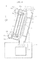
- FIG. 4 is a side sectional view illustrating the configuration, in outline, of the thin-film deposition apparatus according to the first embodiment of the present invention.
- a thin-film deposition apparatus 1 includes a film deposition chamber 6, a counter electrode 2, a heat equalizer plate 5, a heat-equalizer-plate holding mechanism 11, a discharge electrode 3, an back plate 4, a supporting section 7, a radio-frequency power feeding path 12 (12a and 12b), matching boxes 13 (13a and 13b), a high-vacuum evacuating section 19, a low-vacuum evacuating section 17, and a table 18.
- components associated with gas supply are omitted.
- the film deposition chamber 6 is a vacuum vessel, and a film is deposited therein on a substrate 8.
- the film deposition chamber 6 is supported on the table 18.
- the counter electrode 2 is a metal plate having a holding section (not shown) for holding the substrate 8.
- the counter electrode 2 is an electrode (for example, the grounding side) opposing the discharge electrode 3 when depositing a film.
- the substrate is held such that one side of the counter electrode 2 closely contacts with the surface of the heat equalizer plate 5, and the other side closely contacts with the surface of the substrate 8 when depositing a film.
- the heat equalizer plate 5 makes the temperature of the contacting counter electrode 2 uniform so as to maintain the temperature of the entire plate substantially uniform.
- the heat equalizer plate 5 is constructed of a non-magnetic material having good heat conductivity and, preferably, having corrosion resistance against fluorine when performing self-cleaning, e.g., aluminum alloy or Ni alloy such as inconel.
- the heat equalizer plate 5 acts as a path of heat, and thus, the temperature distribution of the member can be spread out.
- the heat equalizer plate 5 is capable of controlling its own temperature by circulating a temperature-controlled heating medium therein or incorporating a temperature-controlled heater therein.
- the heat-equalizer-plate holding mechanism 11 holds the heat equalizer plate 5 and the counter electrode 2 such that the heat equalizer plate and the counter electrode are substantially parallel to the side surface of the film deposition chamber 6. Then, when depositing a film, the heat-equalizer-plate holding mechanism 11 moves the heat equalizer plate 5, the counter electrode 2, and the substrate 8 closer to the discharge electrode 3.
- the discharge electrode 3 is separated into a plurality of ladder-type electrodes.
- the discharge electrode 3 receives high-frequency electrical power from a feeding point 53 connected to the radio-frequency power feeding path 12a and a feeding point 54 connected to the radio-frequency power feeding path 12b.
- the discharge electrode 3 becomes an electrode (for example, the high-frequency electrical power input side) opposing the counter electrode 2 (for example, the grounding side).
- a film is deposited on the substrate 8 by plasma generated by an electrical discharge between the discharge electrode 3 and the counter electrode 2.
- the depostion preventing plate 4 is grounded, and restricts the area where a film is deposited by restricting the area where the plasma spreads out. In the case of Fig.
- the supporting section 7 extends inward from the side surface of the film deposition chamber 6, perpendicularly with respect to the discharge electrode 3.
- the supporting section 7 is engaged with the back plate 4 to hold the back plate 4 so as to cover the space on a side of the discharge electrode 3 opposite to the counter electrode 2.
- the supporting section 7 is connected to the discharge electrode 3 in an insulated manner and holds the discharge electrode 3 substantially parallel to the side surface of the film deposition chamber 6.
- the matching boxes 13 are capable of matching the impedance at the outputs.
- High-frequency electrical power is supplied from a radio-frequency power supply, which is not shown, via a radio-frequency power feeding path 14 (14a and 14b).
- the high-frequency electrical power is supplied to the discharge electrode 3 via the radio-frequency power feeding path 12 (12a and 12b).
- a heating medium is supplied from a heating-medium supplying device (not shown) to the matching box 13b via a heating-medium supplying pipe 15b, and is supplied to the discharge electrode 3 via the radio-frequency power feeding path 12b and the feeding point 54.
- the heating medium is supplied from the discharge electrode 3 via the feeding point 53 and the radio-frequency power feeding path 12a and is sent to the heating-medium supplying device via a heating-medium supplying pipe 15a.
- the temperature of the heating medium is controlled by the heating-medium supplying device (for example, PID control based on the difference between the measured temperature and a set value), and thus, the temperature of the discharge electrode 3 can be maintained at a predetermined temperature.
- the heating medium can be spread throughout the discharge electrode 3, without generating sites where the heating medium is accumulated or does not reach.
- the radio-frequency power feeding path 12 (12a and 12b) allows the heating medium to pass through, for example, a narrow pipe provided at the center area of the circular pipe of the radio-frequency power feeding path 12 and transfer electrical power through the circumferential section. Instead, the configuration may be opposite of that described above. Furthermore, a pipe exclusively used for the heating medium may be provided.
- the radio-frequency power feeding path 12 is vacuum-sealed by an O-ring provided in the wall of the film deposition chamber 6. One end of the radio-frequency power feeding path 12 is electrically connected to the discharge electrode 3, and the other end is electrically connected to the matching boxes 13. The high-frequency electrical power from the matching boxes 13 is supplied to the discharge electrode 3.
- the high-vacuum evacuating section 19 includes a high vacuum pump and an on-off valve for evacuating gas inside the film deposition chamber 6.
- the low-vacuum evacuating section 17 includes a roughin vacuum pump and an on-off valve for evacuating gas inside the film deposition chamber 6.
- the table 18 holds the film deposition chamber 6. There is an area containing the low-vacuum evacuating section 17 inside the table 18.
- the surface of the counter electrode 2 in contact with the substrate 8 is faced upward at an angle of 7° to 12° with respect to the z direction. It is preferable to slightly tilt the substrate 8 from the vertical direction because the substrate 8 can be easily supported with its own weight, and the installation area in the film deposition chamber 6 can thus be reduced.
- Fig. 5 is a partial perspective view of part of the configuration of the thin-film deposition apparatus according to the first embodiment of the present invention. Directions are indicated by arrows in the drawing.
- the discharge electrode 3 includes ladder-type electrodes.
- the discharge electrode 3 includes eight ladder-type electrodes, i.e., discharge electrodes 3a to 3h.
- the number of ladder-type electrodes is not limited thereto, and any number appropriate for supplying a uniform radio frequency to obtain uniform plasma in order to facilitate fabrication may be selected.
- the discharge electrode 3 may be constructed of one ladder-type electrode.
- Each of the discharge electrodes 3a to 3h includes two lateral structures 20 extending in the X direction substantially parallel to each other and a plurality of longitudinal structures 21 being provided between the two lateral structures 20 and extending in the Y direction, which is substantially orthogonal to the X direction, substantially parallel to one another.
- the Z direction is substantially orthogonal to the X and Y directions.
- the matching box 13a, the radio-frequency power feeding path 14a, the radio-frequency power feeding path 12a, the heating-medium supplying pipe 15a, and a raw-gas pipe 16a are provided on the side of the feeding point 53, and the matching box 13b, the radio-frequency power feeding path 14b, the radio-frequency power feeding path 12b, the heating-medium supplying pipe 15b, and a raw-gas pipe 16b are provided on the side of the feeding point 54.
- the radio-frequency power feeding path 12 is vacuum-sealed by an O-ring provided in the wall of the film deposition chamber 6.
- the matching box 13 only the matching box 13, the radio-frequency power feeding path 14, the radio-frequency power feeding path 12, the heating-medium supplying pipe 15, and the raw-gas pipe 16 that are associated with the discharge electrode 3a are illustrated.
- Each of the discharge electrodes 3a to 3h is connected to the raw-gas pipe 16a near the feeding point 53.
- Raw gas is supplied from the raw-gas pipe 16a.
- the raw-gas pipe 16b is connected near the feeding point 54.
- Raw gas is supplied from the raw-gas pipe 16b.
- Each of the discharge electrodes 3a to 3h ejects the supplied raw gas in the direction indicated by arrows in the drawing, i.e., toward the substrate 8, from the surfaces of the discharge electrodes.
- eight groups of the matching box 13a, the radio-frequency power feeding path 14a, the matching box 13b, and the radio-frequency power feeding path 14b are provided, and electrical power is supplied to the discharge electrodes 3a to 3h by these eight groups.
- the number of groups is not limited to eight.
- the number of feeding points may correspond to the number of discharge electrodes, or electrical power may be supplied by less than eight groups.
- the discharge electrodes 3a to 3h are grouped to correspond to the number of groups to be used.
- Fig. 6 is a schematic block diagram illustrating the configuration associated with high-frequency electrical power supply in the thin-film deposition apparatus according to the first embodiment of the present invention.
- the thin-film deposition apparatus 1 includes a power supply 60.
- the power supply 60 includes an RF amplifier (radio-frequency power supply A) 62, an RF amplifier (radio-frequency power supply B) 63, a radio-frequency (RF) oscillator 64, a radio-frequency (RF) oscillator 65, a selector switch 66, and a function generator 67.
- the radio-frequency oscillator 64 generates, for example, a 60-MHz radio-frequency (RF) signal, and then sends the signal to the RF amplifier 62 and the selector switch 66.
- the radio-frequency oscillator 64 uses a built-in phase shifter to modulate the phase of the radio-frequency.
- the radio-frequency (RF) oscillator 65 generates, for example, a 58.5-MHz radio-frequency (RF) signal, and then sends the signal to the selector switch 66.
- the radio-frequency oscillator 65 uses a built-in phase shifter to modulate the phase of the radio-frequency.
- the frequency may be varied, for example, from 58.5 MHz to 59.9 MHz or from 60.1 MHz to 61.5 MHz.
- the selector switch 66 receives radio-frequency signals from the radio-frequency oscillators 64 and 65, and then supplies the signals to the RF amplifier 63.
- the function generator 67 changes the time ratio, i.e., duty ratio, of the radio-frequency signals.
- the RF amplifier 62 and the RF amplifier 63 function as radio-frequency sources by amplifying and outputting the supplied radio-frequency signals.
- the radio-frequency oscillator 64 generates, for example, a 60-MHz radio-frequency signal, and then sends the signal to the RF amplifier 62 and the selector switch 66.
- the radio-frequency oscillator 65 generates, for example, a 58.5-MHz radio-frequency signal, and then sends the signal to the selector switch 66.
- the selector switch 66 switches the 60-MHz radio-frequency signal sent from the radio-frequency oscillator 64 and the 58.5-MHz radio-frequency signal sent from the radio-frequency oscillator 65 in a constant cycle, and then send the signals to the RF amplifier 63. Therefore, the RF amplifier 62 supplies 60-MHz high-frequency electrical power to the feeding point 53.
- the RF amplifier 63 supplies the high-frequency electrical power of 60 MHz and 58.5 MHz, which are switched in a constant cycle, to the feeding point 54.
- the selector switch 66 switches the 60-MHz radio-frequency signal sent from the radio-frequency oscillator 64 and the 58.5-MHz radio-frequency signal sent from the radio-frequency oscillator 65 on the basis of a signal from the function generator 67.
- the function generator 67 changes the time ratio, i.e., duty ratio, of the switching of the radio-frequency signal according to a signal corresponding to gas conditions, such as gas pressure and gas species.
- the radio-frequency oscillator 64 uses the phase shifter to shift the phase of the radio-frequency signals to be sent to the phase of the RF amplifier 62 and the selector switch 66 with respect to the radio-frequency signal to be sent to the other.
- the radio-frequency oscillator 65 is capable of varying the oscillation frequency, for example, from 58.5 MHz to 59.9 MHz or from 60.1 MHz to 61.5 MHz.
- the discharge electrodes 3a to 3h may receive electrical power from eight respective power supplies 60. Instead, the discharge electrodes 3a to 3h may receive electrical power from less than eight power supplies 60. In such a case, the discharge electrodes 3a to 3h are grouped to correspond to the number of power supplies 60. Moreover, the discharge electrode 3 may be constructed of one ladder-type electrode and may receive electrical power from one power supply 60.
- Figs. 7A to 7C are a plan view and sectional views illustrating the configuration of the discharge electrode according to the first embodiment of the present invention.
- Fig. 7A is a sectional view of the discharge electrode 3a, taken along line BB in Fig. 5 .
- Fig. 7B is a sectional view of the discharge electrode 3a, taken along line AA in Fig. 7A .
- Fig. 7C is a plan view of the bottom of the discharge electrode 3a in Fig. 7A .
- Each of the longitudinal structures 21 (21a) of the discharge electrode 3 (3a) includes an electrode main body 35 having a built-in gas-pipe accommodating space 36, a gas pipe 41 accommodated in the gas-pipe accommodating space 36, and a porous body 40.
- the XYZ directions are the same as those in Fig. 5 .
- the electrode main body 35 includes an opening 38 in the +Z direction; a gas diffusion path 37 that is provided between the gas-pipe accommodating space 36 and the opening 38 and that connects the gas-pipe accommodating space 36 and the opening 38; and a pair of heating-medium flow paths 34 disposed to sandwich the gas diffusion path 37.
- the porous body 40 covers the opening 38, and has many gas ejection holes 40a penetrating through the porous body 40 from the opening 38 side to the opposite side in the Z direction.
- the gas-pipe accommodating space 36, the gas diffusion path 37, the opening 38, and the porous body 40 are arranged in the Z direction in this order, and the porous body 40 is disposed furthest on the +Z side.
- the heating-medium flow paths 34, the gas-pipe accommodating space 36, the gas diffusion path 37, and the opening 38 define a space inside the electrode main body 35, which extends from the end section 35a of the electrode main body 35 to the end section 35b in the Y direction.
- the porous body 40 also extends from the end section 35a to the end section 35b in the Y direction.
- the gas-pipe accommodating space 36 has a center axis S36 that extends in the Y direction.
- the gas pipe 41 includes a pipe main body 42 extending inside the gas-pipe accommodating space 36 from the end section 35a to the end section 35b in the Y direction; and a pipe end section 43 connected to each end of the pipe main body 42.
- the pipe end section 43 projects from the opening where the gas-pipe accommodating space 36 is open at the end section 35a or the end section 35b.
- the gas pipe 41 has a gas flow path 41a as an internal space penetrating through the pipe main body 42 and the pipe end sections 43 in the Y direction.
- the pipe main body 42 has nozzle holes 42c penetrating from a pipe inner surface 42a facing the gas flow path 41a to a pipe outer surface 42b.
- the pipe end section 43 is provided with an annular groove 43a.
- the gas pipe 41 has a center axis S41 extending in the Y direction.
- the electrode main body 35 has an electrode inner surface 39 facing the gas-pipe accommodating space 36.
- the electrode inner surface 39 faces the pipe outer surface 42b, with a gap between the electrode inner surface and the pipe outer surface 42b.
- the electrode inner surface 39 includes an electrode-inner-surface first section 39a, which is a section on the side opposite to the gas diffusion path 37, and an electrode-inner-surface second section 39b, which is a section on the gas diffusion path 37 side.
- the electrode-inner-surface first section 39a and the electrode-inner-surface second section 39b extend in the Y direction.
- the lateral structure 20 includes a header 30, which is a section on the -Z side of the lateral structure 20, and a base 33, which is a section on the +Z side of the lateral structure 20.
- the header 30 and the base 33 extend in the X direction.
- the base 33 is connected to the plurality of electrode main bodies 35 at the respective end sections 35a (or end sections 35b).
- the base 33 and the electrode main body 35 may be integrated into one unit.
- the base 33 is provided with a heating-medium flow path 34'.
- the heating-medium flow path 34' is a space extending inside the base 33 in the X direction, and communicates with the respective heating-medium flow paths 34 of the plurality of electrode main bodies 35.
- the heating-medium flow path 34' of one of the lateral structures 20 communicates with the heating-medium supplying pipe 15a, and the heating-medium flow path 34' of the other lateral structure 20 communicates with the heating-medium supplying pipe 15b.
- the header 30 is provided with depressions 31 and a gas flow path 32.
- the same number of depressions 31 as the number of longitudinal structures 21a connected to the lateral structure 20 is provided, and, therefore, the same number of depressions 31 as the number of the electrode main bodies 35 and the gas pipes 41 is provided (see Fig. 12 ).
- the depression 31 has a bottom surface 31a and a sidewall 31b.
- the gas flow path 32 is a space extending inside the header 30 in the X direction, and communicates with each of the depressions 31.
- the gas flow path 32 of one of the lateral structures 20 communicates with the raw-gas pipe 16a, and the gas flow path 32 of the other lateral structure 20 communicates with the raw-gas pipe 16b.
- the header 30 is attached to the end section 35a (or end section 35b) of the electrode main body 35 such that the pipe end section 43 is inserted into the depression 31. At this time an O-ring 49 disposed in the annular groove 43a seals the gap between the pipe end section 43 and the header 30. As the material of the O-ring 49, it is preferable to use Kalrez (trademark) that has excellent gas resistance and high-temperature resistance.
- the header 30 is attached to each of the plurality of electrode main bodies 35 with bolts 48. Therefore, the headers 30 are removable from the plurality of electrode main bodies 35 and the bases 33.
- the discharge electrode 3a has a structure using the porous body 40 in order to make the gas distribution on the substrate 8 uniform so that it is suitable for fabrication of a microcrystalline solar cell, in which the thin film is deposited at high pressure.
- the manufacturing cost of the discharge electrode 3a tends to increase.
- the discharge electrode 3a when removing the header 30 from the electrode main body 35, it is possible to carry out maintenance of the nozzle holes 42c by removing the gas pipe 41 in a direction parallel to the center axis S41. With such a structure, it is possible to suppress the manufacturing cost of the discharge electrode 3a.
- the gas pipe 41 does not require blast cleaning, and the maintenance cost is thus suppressed.
- One end of the gas flow path 41a communicates with the raw-gas pipe 16a via the depressions 31 and the gas flow path 32 of one of the lateral structures 20.
- the other end communicates with the raw-gas pipe 16b via the depressions 31 and the gas flow path 32 of the other lateral structure 20.
- Raw gas for film deposition supplied from the raw-gas pipe 16a and the raw-gas pipe 16b flows through the gas flow path 41a.
- the gas flowing through the gas flow path 41a is ejected from the nozzle holes 42c.
- nozzle holes 42c are small holes arranged with appropriate intervals in the Y direction, and eject gas in a substantially uniform manner from the gas flow path 41a toward the electrode inner surface 39.
- the gas ejected from the nozzle holes 42c is diffused through a gap between the pipe outer surface 42b and the electrode inner surface 39 in the Y direction, and flows into the gas diffusion path 37.
- the gas moves in the +Z direction while being diffused through the gas diffusion path 37 in the Y direction, and then reaches the opening 38.
- the gas diffuses through the opening 38 in the X direction and reaches the porous body 40 because the flow path width (X direction) of the opening 38 is larger than the flow path width (X direction) of the gas diffusion path 37.
- the gas is ejected from the gas ejection holes 40a into the space between the substrate 8 and the discharge electrode 3a.
- the porous body 40 is provided so as to cover a large portion of the surface of the substrate 8 side of the longitudinal structures 21a. In this way, the gas can be substantially uniformly supplied to the substrate 8 on the counter electrode 2.
- the porous body 40 may be a porous plate having a relatively small thickness in the Z direction, or may be formed of a block having a relatively large thickness in the Z direction and many smaller holes.
- the nozzle holes 42c face the electrode inner surface and not the gas diffusion path 37, the gas ejected from the nozzle holes 42c travels a long distance before reaching the gas diffusion path 37, and the traveling direction of the gas changes while traveling. As a result, diffusion of the gas in the gap between the pipe outer surface 42b and the electrode inner surface 39 is enhanced. It is especially preferable that the nozzle holes 42c face the electrode-inner-surface first section 39a. However, even when they face the electrode-inner-surface second section 39b, the changes in the traveling distance and the traveling direction of the gas are maintained at a certain level.
- the porous body 40 is preferably made of a metal that is a non-magnetic material with good heat conductivity and has fluorine resistance when self-cleaning (reactive ion etching). Furthermore, it is preferably a metal that can be easily welded. An example of such a metal is aluminum material (aluminum or aluminum alloy). This is also preferable for the electrode main bodies 35.
- the shape of the gas ejection holes 40a is not limited. In addition to a circle, any appropriate shape, such as an oval, a rectangle, a triangle, or a star, may be used.
- the gas ejected from the gas ejection holes 40a into the space between the discharge electrode 3 (discharge electrode 3a) and the substrate 8 (or the counter electrode 2) contributes to the reaction for film deposition or the reaction for self-cleaning, and generates a production gas by the reaction.
- the gap 22 between the adjacent longitudinal structures 21a acts as a path for evacuating remaining gas that did not contribute to the reactions or other generated gases. Since evacuation is carried out through the gap 22, it is possible to deposit a uniform film on the substrate 8. Since the nozzle holes 42c eject gas in a direction (-Z direction) opposite to the substrate 8, the gas flow path from the nozzle holes 42c to the substrate 8 is long and winding. Therefore, the gas is sufficiently diffused before reaching the substrate 8, and the flow distribution and the concentration distribution of the gas on the substrate 8 is made uniform.
- One end of the heating-medium flow path 34 is connected to the heating-medium supplying pipe 15a via the heating-medium flow path 34' of one of the lateral structures 20.
- the other end is connected to the heating-medium supplying pipe 15b via the other lateral structure 20. Since the temperature-controlled heating medium is circulated through the heating-medium flow path 34, the electrode main body 35 can be regulated at a desired temperature.
- two heating-medium flow paths 34 are provided in one electrode main body 35. However, one or three or more heating-medium flow paths 34 may be provided.
- the heating-medium flow paths 34 is not required when the electrical power applied between the discharge electrode and the counter electrode is small and when temperature control is not necessarily required.
- Fig. 8 is a transparent view of the surroundings of the pipe main body 42 of the discharge electrode shown in Figs. 7A to 7C .
- the nozzle holes 42c are arranged in the pipe main body 42 in the Y direction at a nozzle pitch L.
- the nozzle diameter d of the nozzle holes 42c is determined so as to satisfy Equation (1): 5 ⁇ ⁇ ⁇ D / 2 2 / ⁇ ⁇ d / 2 2 ⁇ N
- D represents the inner diameter of the pipe main body 42
- N represents the number of nozzle holes 42c provided on one pipe main body 42.
- Equation (1) indicates that a flow path sectional area S1 of the pipe main body 42 is five times larger than the total ejection area S2 of the nozzle holes 42c provided in one pipe main body 42.
- Fig. 9 is a graph illustrating the relationship between the sectional area ratio and the flow rate distribution of the discharge electrode 3a.
- the vertical axis represents the flow rate distribution, and the horizontal axis represents the sectional area ratio S1/S2.
- the flow rate distribution increases when the sectional area ratio S1/S2 decreases. When the sectional area ratio S1/S2 becomes less than 5, the flow rate distribution suddenly increases.
- Equation (1) can be represented as the following Equation (1'): 0 ⁇ ⁇ ⁇ d / 2 2 ⁇ N / ⁇ ⁇ D / 2 2 ⁇ 1 / 5
- the pipe main body 42 may be a rectangular pipe or an oval pipe, and the nozzle holes 42c may be rectangular or oval.
- gas is ejected uniformly from the nozzle holes 42c when the flow path sectional area S1 of the pipe main body 42 and the total ejection area S2 of the nozzle holes 42c provided in one pipe main body 42 satisfy the relationship in Equation (1').
- Equation (2) indicates that the flow path sectional area (2wL) of the gap between the pipe outer surface 42b and the electrode inner surface 39 corresponding to one nozzle hole 42c is greater than the ejection area S of one nozzle hole 42c.
- Equation (2) the flow speed of the gas ejected from the nozzle holes 42c becomes smaller than the ejection speed at the nozzle holes 42c while the gas moves toward the gas diffusion path 37 in the gap between the pipe outer surface 42b and the electrode inner surface 39, and thus, the distribution of the gas ejected from the porous body 40 in the X direction becomes uniform.
- Equation (2) can be represented as the following Equation (2'): 0 ⁇ ⁇ ⁇ d / 2 2 / 2 ⁇ wL ⁇ 1
- the nozzle holes 42c are not limited to circles, and may be rectangles or ovals.
- gas is ejected uniformly from the nozzle holes 42c when the flow path sectional area (2wL) of the gap between the pipe outer surface 42b and the electrode inner surface 39 associated with one nozzle hole 42c and the ejection area S of one nozzle hole 42c satisfy the relationship in Equation (2').
- the upper limit of the gap distance w is restricted by the size of the discharge electrode 3a.
- Figs. 10A and 10B are transparent views of the surroundings of the pipe main body 42 of the discharge electrode shown in Figs. 7A to 7C .
- Figs. 10A and 10B illustrate spacers 44 disposed between the pipe outer surface 42b and the electrode inner surface 39 in order to maintain a constant gap distance w.
- the spacer 44 shown in Fig. 10A is annular, and is provided around the entire circumference of the pipe outer surface 42b.
- the spacers 44 shown in Fig. 10B are projections provided on the circumference of the pipe outer surface 42b at equiangular intervals.
- the spacers 44 are provided in the Y direction at appropriate intervals.
- a plurality of spacers 44 e.g., four or five, is provided on one pipe main body 42.
- the spacers 44 may be provided on the pipe outer surface 42b, as shown in Figs. 10A and 10B , or, instead, may be provided on the electrode inner surface 39.
- Fig. 11 illustrates the relationship between the flow rate distribution in the discharge electrode 3a and the misalignment of the gas pipe and the center axis of the electrode.
- the vertical axis represents the flow rate distribution.
- the horizontal axis represents the ratio of the vertical misalignment of the center axis S36 and the center axis S41 shown in Fig. 7B , to the gap distance w when the center axes S36 and S41 are aligned.
- the numerator represents the misalignment
- the denominator represents the gap distance w.
- flow rate distribution maximum value of flow rate - minimum value of flow rate / 2 / average flow rate
- the spacers 44 on the pipe outer surface 42b such that the spacers 44 contact the electrode inner surface 39 before the vertical misalignment of the center axis S36 and the center axis S41 with respect to the center axis S36 exceeds 25% of the gap distance w when the center axes S36 and S41 are aligned.
- the height of the spacers 44 from the pipe outer surface 42b be in the range between 75% or more and less than 100% of the gap distance w when the center axis S36 and the center axis S41 are aligned.
- the spacers 44 be provided such that the spacers 44 contact the pipe outer surface 42b before the vertical misalignment of the center axis S36 and the center axis S41 with respect to the center axis S36 exceeds 25% of the gap distance w when the center axes S36 and S41 is aligned.
- the height of the spacers 44 from the electrode inner surface 39 be in the range between 75% or more and less than 100% of the gap distance w when the center axis S36 and the center axis S41 are aligned.
- the gas pipe 41 By constructing the gas pipe 41 with aluminum material (aluminum or aluminum alloy), which is the same material as the electrode main body 35, the gap between the pipe outer surface 42b and the electrode inner surface 39 is prevented from being reduced due to thermal expansion.
- aluminum material aluminum or aluminum alloy
- non-magnetic stainless steel examples are SUS304 and SUS316.
- Stainless steel is selected in consideration of corrosion resistance against fluorine when performing self-cleaning.
- the stainless steel is non-magnetic in view of resistance against the plasma.
- the linear expansion coefficient 17 ⁇ 10 -6 of SUS304 is close to the linear expansion coefficient 24 ⁇ 10 -6 of aluminum material, the gap between the pipe outer surface 42b and the electrode inner surface 39 is prevented from being reduced due to thermal expansion.
- the O-ring 49 sealing the gap between the pipe end section 43 and the header 30 may be disposed in the annular groove 43a provided in the pipe end section 43, as shown in Fig. 7B , or may be disposed in an annular groove 31c provided in the sidewall 31b, as shown in Fig. 13 . In the configuration shown in Fig. 13 , it is preferable that the distance L1 between the bottom surface 31a and the annular groove 31c be greater than 10 mm.
- the distance L1 is the distance in the direction that the pipe end section 43 is inserted into the depression 31.
- a gas pipe that has a length of 1 m or greater is used as the gas pipe 41 in order to deposit a film on a substrate 8 with a side of 1 m or longer. Therefore, it is preferable to set the distance L1 greater than 10 mm so that, even when a difference occurs in the thermal expansion of the gas pipe 41 and the electrode main body 35, deformation does not occur in the gas pipe 41 and gas does not leak from the sealed portion.
- the distance L1 greater than 10 mm expansion or contraction of the gas pipe 41 of about ⁇ 5 mm can be absorbed. It is especially effective to set the distance L1 in this way when the materials of the gas pipe 41 and the electrode main body 35 differ.
- Figs. 14A and 14B illustrate a key structure for adjusting the orientation of the nozzle hole 42c on the gas pipe 4.
- Fig. 14B is a transparent view of the key structure shown in Fig. 7B .
- the annular spacer 44 is provided on the pipe outer surface 42b, and the annular spacer 44 has a key groove 44a.
- a key 45 is provided on the electrode main body 35 such that the key 45 projects from the electrode inner surface 39 into the gas-pipe accommodating space 36.
- the key 45 and the key groove 44a engages, and the orientation of the nozzle hole 42c is adjusted to face the side opposite to the porous body 40, i.e., to face the electrode-inner-surface first section 39a.
- the key structure may have the structure shown in Fig. 14A .
- the key structure includes a key 45 provided on the outer surface of the pipe end section 43 and a key groove 31d provided on the sidewall 31b.
- the annular groove 43a is disposed closer to the end than the key 45 is.
- FIG. 15A illustrates a case in which the pipe main body 42 is a rectangular pipe and the cross-section of the gas-pipe accommodating space 36 is rectangular.
- Fig. 15B illustrates a case in which the pipe main body 42 is an oval pipe and the cross-section of the gas-pipe accommodating space 36 is oval. As shown in Fig.
- silicon-based thin-film solar cell includes silicon (Si), silicon carbide (SiC), and silicon germanium (SiGe).
- SiGe silicon germanium
- an example of silicon-based thin film is microcrystalline silicon or amorphous silicon.
- a transparent conductive film mainly composed of a tin oxide film is deposited on the surface of the substrate 8 with a thickness of approximately 500 to 800 nm using a thermal CVD apparatus at a deposition temperature of approximately 500°C.
- a transparent conductive film and an amorphous silicon solar cell layers are formed on the substrate 8.
- the film deposition chamber 6 is set to a predetermined vacuum level (for example, 10 -6 Pa).
- the heat equalizer plate 5 is controlled such that the temperature of the counter electrode 2 is set constant at, for example, 200°C.
- the distance between the substrate and the electrode is, for example, 2 to 15 mm; for example, 5 mm is preferable for making the film thickness and the film quality uniform and performing high-speed deposition.
- Gas for film deposition is supplied to the space between the discharge electrode 3 and the substrate 8 through the raw-gas pipe 16a, the gas flow path 32, the depressions 31, the gas flow path 41a, the nozzle holes 42c, the gap between the pipe outer surface 42b and the electrode inner surface 39, the gas diffusion path 37, the opening 38, and the porous body 40 (plurality of holes 40a).
- the gas is, for example, H 2 +SiH 4 (SiH 4 partial pressure: 2% to 20%).
- SiH 4 SiH 4 partial pressure: 2% to 20%
- a dopant is added to the gas.
- the range of deposition pressure is, for example, 800 to 1800 Pa when depositing a microcrystalline silicon thin film.
- the range of deposition pressure is 200 to 600 Pa when depositing an amorphous silicon thin film.
- the gas is supplied through the gas ejection holes 40a and is evacuated from the gap 22.
- Predetermined high-frequency electrical power is supplied to the discharge electrode 3 via the radio-frequency power feeding path 12 connected to the output while the impedance at the output of the matching box 13 is matched. In this way, plasma is generated between the discharge electrode 3 and the counter electrode 2, and then a silicon thin film is deposited on the substrate 8.
- the high-frequency electrical power, the substrate temperature, and the film thickness are, for example, 1 W/cm 2 , 200°C, and 1.5 to 3 ⁇ m, respectively.
- the high-frequency electrical power, the substrate temperature, and the film thickness are, for example, 0.2 W/cm 2 , 200°C, and approximately 300 nm, respectively.
- the heating medium is made to flow to the heating-medium flow paths 34 provided inside the discharge electrode 3 through the heating medium supplying pipe provided inside the radio-frequency power feeding path 12.
- the temperature of the discharge electrode 3 is controlled.
- the temperature of the electrode main body 35 is controlled at an appropriate temperature between, for example, 50°C to 180°C. In other words, the temperature of the electrode main body 35 is controlled according to the heat balance of the substrate heating temperature during deposition, the plasma input electrical power, and the heat emitted by the film deposition chamber 6 such that warpage of the substrate caused by a temperature difference between the front and back of the substrate 8 is suppressed.
- Steps 1 to 4 are repeated for depositing the p-layer silicon thin film, the i-layer silicon thin film, and the n-layer silicon thin film.
- a back-side conductive film of silver or aluminum is formed on the n layer with a sputtering apparatus to produce a solar cell.
- the p-layer silicon thin film, the i-layer silicon thin film, and the n-layer silicon thin film may be deposited in different film deposition chambers 6, respectively. Furthermore, the p-layer silicon thin film, the i-layer silicon thin film, and the n-layer silicon thin film may be deposited with different thin-film deposition apparatuses. Other thin films may be interposed therebetween if necessary. For these other films, transparent conductive films, and back-side conductive films, the thin-film deposition apparatus according to the present invention does not have to be used. Although not described in particular, a film etching process using a YAG laser is carried out as a step of the process in order to have a serially integrated structure of the solar cell.
- the present invention is not limited to such an example, and may be also applied to other types of thin-film solar cells, such as a multi-junction solar cell in which one or a plurality of amorphous silicon solar cells and one or a plurality of microcrystalline silicon solar cells are stacked.
- the present invention may also be applied to a solar cell produced on a non-transmissive substrate, such as a metal substrate in which light is incident from the side opposite to a substrate.
- the gas ejected in the +Z direction from the plurality of gas ejection holes 40a to the substrate 8 contributes to plasma generation, while part of the gas moves below the adjacent longitudinal structure 21a.
- the discharge electrode 3 of the present invention since the gap 22 between adjacent longitudinal structures 21a is smaller than the distance between the electrode and the substrate, e.g., 2 to 4 mm, and a flat plate or block porous body is used as the porous body 40, the counter electrode 2 side of the discharge electrode 3 can be substantially flattened. In this way, the generation of plasma can be made more uniform, and thus the film thickness and film quality can be made more uniform. As described above, according to the present invention, the occurrence of a film thickness distribution and a film quality distribution can be suppressed even when film deposition is carried out in the condition of narrow gap between the substrate and the electrode and the high deposition pressure is increased. Moreover, by performing high-speed deposition while suppressing the generation of a film thickness distribution and a film quality distribution, productivity can be improved.
- the configuration of a thin-film deposition apparatus according to a second embodiment of the present invention will be described.
- the configuration of the discharge electrode 3 differs from that in the first embodiment.
- the configuration of the thin-film deposition apparatus according to the second embodiment of the present invention and the configuration associated with the high-frequency electrical power supply in the thin-film deposition apparatus according to the second embodiment of the present invention are the same as those in the first embodiment shown in Figs. 4 to 6 . Therefore, descriptions thereof are omitted.
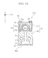
- Fig. 16 is a lateral sectional view (B-B cross-section in Fig. 5 ) of a longitudinal structure of a discharge electrode according to the second embodiment of the present invention.
- the XYZ directions are the same as those in Fig. 5 .
- the electrode main body 35 corresponding to the longitudinal structure 21 (21a) of the first embodiment can be separated into an electrode-main-body first section 46 that is a section on the +Z side, and an electrode-main-body second section 47 that is a section on the -Z side.
- the electrode-main-body first section 46 and the base 33 are integrated; the base 33 and the header 30 are integrated; and the gas pipe 41 and the header 30 are integrated.
- the discharge electrode 3a of the second embodiment has the same structure as the discharge electrode 3a of the first embodiment, except that the electrode-main-body second section 47 is removable from the structure including the porous body 40, the electrode-main-body first section 46, the base 33, the header 30, and the gas pipe 41.
- the heating-medium flow paths 34 are omitted.
- the electrode-main-body first section 46 includes the opening 38, the gas diffusion path 37, and the electrode-inner-surface second section 39b.
- the porous body 40 covers the opening 38.
- the electrode-main-body second section 47 includes the electrode-inner-surface first section 39a.
- the electrode-main-body second section 47 is attached in a removable manner to the electrode-main-body first section 46 with bolts 48.
- the gas-pipe accommodating space 36 which is an inner space of the electrode main body 35, is formed.
- the gas-pipe accommodating space 36 is a space interposed between the electrode-main-body first section 46 and the electrode-main-body second section 47 for accommodating the pipe main body 42.
- the solar cell fabrication method according to the second embodiment is the same as that according to the first embodiment, except for the discharge electrode shown in Fig. 16 , descriptions thereof are omitted. Since the discharge electrode 3a in the second embodiment can be separated, maintenance of the nozzle hole 42c can be easily carried out.
- the configuration of a thin-film deposition apparatus according to a third embodiment of the present invention will be described.
- the configuration of the discharge electrode 3 differs from those according to the first and second embodiments.
- the configuration of the thin-film deposition apparatus according to the third embodiment of the present invention and the configuration associated with the high-frequency electrical power supply in the thin-film deposition apparatus according to the third embodiment of the present invention are the same as those in the first embodiment shown in Figs. 4 to 6 . Therefore, descriptions thereof are omitted.
- Fig. 17 is a lateral sectional view (B-B cross-section in Fig. 5 ) of a discharge electrode according to the third embodiment of the present invention.
- the XYZ directions are the same as those in Fig. 5 .
- the plurality of longitudinal structures 21 (21b) of the discharge electrode 3a of the third embodiment each include an electrode main body 71, which is a section on the +Z side; a gas block 76, which is a section on the -Z side; and a porous body 40', which is similar to the porous body 40.
- Each of the electrode main body 71 and the gas block 76 has one end connected to one of the lateral structures 20 and the other end connected to the other lateral structure 20.
- the former lateral structure 20 is connected to the radio-frequency power feeding path 12a, and the latter lateral structure 20 is connected to the radio-frequency power feeding path 12b.
- the electrode main body 71 includes an opening 72 that is open toward the counter electrode 2 where the substrate 8 is held; an attachment section 73 that is disposed on the side opposite to the opening 72; a gas diffusion path 74 that is provided between the opening 72 and the attachment section 73 and communicates with the opening 72; and an opening 75 where the gas diffusion path 74 opens at the attachment section 73; and a pair of heating-medium flow paths 80 that are disposed so as to sandwich the gas diffusion path 74.
- One of the heating-medium flow paths 80 is disposed on the +X side of the gas diffusion path 74, and the other heating-medium flow path 80 is disposed on the -X side of the gas diffusion path 74.
- the porous body 40' covers the opening 72 and is provided with gas ejection holes 40a' that penetrate the porous body 40' in the Z direction from the opening 72 side to the opposite side.
- the attachment section 73, the gas diffusion path 74, the opening 72, and the porous body 40' are arranged in the Z direction in this order.
- the porous body 40' is disposed furthest on the +Z side.
- the substrate 8 held by the counter electrode 2 is disposed on the +Z side of the porous body 40'.
- the opening 72, the gas diffusion path 74, and the heating-medium flow path 80 define a space extending in the Y direction inside the electrode main body 71 from one end of the electrode main body 71 to the other end.
- the heating-medium flow path 80 is connected to the heating-medium supplying pipe 15a and the other end is connected to the heating-medium supplying pipe 15b so as to circulate the heating medium.
- the opening 75 and the porous body 40' also extend in the Y direction from one end of the electrode main body 71 to the other end.
- the attachment section 73 is a depressed groove extending in the Y direction from one end of the electrode main body 71 to the other end.
- the opening 75 opens at the bottom surface of this groove.
- the gas block 76 includes a gas flow path 77; an attachment section 78; and nozzle holes 79 that are disposed between the gas flow path 77 and the attachment section 78 to communicate with the gas flow path 77, and open at the attachment section 78.
- the gas flow path 77, the nozzle holes 79, and the attachment section 78 are arranged in the Z direction in this order.
- the attachment section 78 is disposed furthest on the +Z side.
- the gas flow path 77 is a space extending inside the gas block 76 in the Y direction from one end of the gas block 76 to the other end. One end of the gas flow path 77 communicates with the raw-gas pipe 16a and the other end communicates with the raw-gas pipe 16b so as to circulate the gas.
- the nozzle holes 79 extend in the Z direction, and are arranged in the Y direction at appropriate intervals.
- the attachment section 78 is a projecting ridge extending in the Y direction from one end of the gas block 76 to the other end.
- the nozzle holes 79 open at the top surface of the ridge.
- the gas block 76 is attached to the electrode main body 71 such that the attachment section 73 and the attachment section 78 engage. Since the gas block 76 is secured to the electrode main body 71 with bolts 48, the gas block 76 is removable from the electrode main body 71. With the gas block 76 being attached to the electrode main body 71, the bottom surface of the attachment section 73 and the top surface of the attachment section 78 closely contact each other, and the nozzle holes 79 communicate with the gas diffusion path 74.
- the gas flow is indicated by arrows.
- the gas ejected into the gas diffusion path 74 through the raw-gas pipe 16a, the gas flow path 77, and the nozzle holes 79 moves in the +Z direction while being diffused in the Y direction through the gas flow path 77, and then reaches the opening 72.
- the gas diffuses through the opening 72 in the X direction to reache the porous body 40' because the flow path width (X direction) of the opening 72 is larger than the flow path width (X direction) of the gas diffusion path 74.
- the gas is ejected from the gas ejection holes 40a' into the space between the substrate 8 and the discharge electrode 3a.
- the porous body 40' is provided so as to cover a large portion of the surface of the substrate 8 side of the longitudinal structures 21b. In this way, the gas can be substantially uniformly supplied to the substrate 8 on the counter electrode 2.
- the porous body 40' may be a porous plate having a relatively small thickness in the Z direction or may be formed of a block having a relatively large thickness in the Z direction and having many smaller holes.
- the porous body 40' enables gas to be supplied more uniformly to the substrate 8.
- the porous body 40' is preferably made of a metal that is a non-magnetic material with good heat conductivity and has fluorine resistance when performing self-cleaning (reactive ion etching). It is preferably a metal that can be easily welded.
- An example of such a metal is aluminum material (aluminum or aluminum alloy). This is also preferable for the electrode main body 71 and the gas block 76.
- the shape of the gas ejection holes 40a' is not limited. In addition to a circle, any appropriate shape, such as an oval, a rectangle, a triangle, or a star, may be used.
- the gas ejected from the gas ejection holes 40a' into the space between the discharge electrode 3 (discharge electrode 3a) and the substrate 8 (or the counter electrode 2) contributes to the reaction for film deposition or the reaction for self-cleaning, and generates a product gas by the reaction.
- the gap 22 between adjacent the longitudinal structures 21a acts as a path for evacuating remaining gas that did not contribute to the reactions or generated gases. Since evacuation is carried out through the gap 22, it is possible to deposit a uniform film on the substrate 8.
- the flow path sectional area of the gas flow path 77 be five times larger than the total ejection area of the nozzle holes 79 communicating with a single gas flow path 77. In this way, gas is uniformly ejected from the plurality of nozzle holes 79.
- the solar cell fabrication method according to the third embodiment is the same as that according to the first embodiment, except for the discharge electrode shown in Fig. 17 , descriptions thereof are omitted.
- the attachment section 73 which is an engagement structure on the electrode main body 71 side
- the attachment section 78 which is an engagement structure on the gas block 76 side
- the depression and protrusion may be switched.
- the discharge electrode 3a according to the third embodiment has a structure using the porous body 40' in order to make the gas distribution on the substrate 8 uniform so that it is suitable for production of a microcrystalline solar cell at high depostion pressure. Also for the discharge electrode 3a in the third embodiment, since the gas block 76 and the electrode main body 71 can be separated, maintenance of the nozzle holes 79 can be easily carried out. Since the discharge electrode 3a in the first and second embodiments does not have an engagement structure that requires highly precise processing, like the discharge electrode 3a in the third embodiment, manufacturing costs are reduced.
Landscapes
- Chemical & Material Sciences (AREA)
- Engineering & Computer Science (AREA)
- Plasma & Fusion (AREA)
- Physics & Mathematics (AREA)
- Analytical Chemistry (AREA)
- General Chemical & Material Sciences (AREA)
- Chemical Kinetics & Catalysis (AREA)
- Materials Engineering (AREA)
- Mechanical Engineering (AREA)
- Metallurgy (AREA)
- Organic Chemistry (AREA)
- Power Engineering (AREA)
- Microelectronics & Electronic Packaging (AREA)
- Chemical Vapour Deposition (AREA)
- Photovoltaic Devices (AREA)
Abstract
Description
- The present invention relates to a discharge electrode used for plasma generation, a thin-film deposition apparatus using the same, and a solar cell fabrication method.
- With thin-film depositing apparatuses for depositing thin films for amorphous silicon solar cells, microcrystalline silicon solar cells, and thin film transistors (TFTs), the area of the substrate has been increased from the viewpoint of improving fabrication efficiency. When depositing a film on such a large area substrate (for example, larger or equal to 1 m × 1 m), it is efficient to employ a method using high-frequency plasma. When using high-frequency plasma, it is effective to use a film deposition method employing a ladder-type electrode, instead of using a film deposition apparatus with a simple parallel-plate-type electrode. As such as film deposition method according to the related art, a known technique using a ladder electrode is disclosed in Japanese Unexamined Patent Application, Publication No.
2002-322563 - To reduce costs of a tandem solar cell including a microcrystalline layer, high-speed deposition is required since the film thickness of the microcrystalline i layer, which is the power generating layer, is several µm and is five to ten times greater than the film thickness of the amorphous silicon i layer. To form a high-quality power generating layer at high speed, it is necessary to employ a high-pressure narrow-gap method, described in Japanese Unexamined Patent Application, Publication No.
2005-150317 Fig. 1 is a diagram illustrating the relationship between a cross-section of an electrode according to a case in which a high-pressure narrow-gap method according to the related art is employed and the deposition speed distribution in local areas corresponding to the shape change in an electrode. The upper half of the drawing is a sectional view of the structure associated with film deposition, and the bottom half illustrates the relationship between the structure and the film thickness. The vertical axis represents film thickness, and the horizontal axis represents positions on the substrate. Aladder discharge electrode 103 of the film deposition apparatus includes a plurality ofcylindrical electrodes 121a. The plurality ofelectrodes 121a faces thesubstrate 108 on the counter electrode (not shown). Deposition gas flows through agas flow path 131 inside theelectrodes 121a, and part of the gas is ejected from a plurality ofgas ejection holes 137. Plasma is generated by electrical power applied between thedischarge electrode 103 and the counter electrode, and deposition gas is decomposed and combined to deposit a film on thesubstrate 108. However, in the high-pressure narrow-gap method, a film thickness distribution is caused by local structures of thedischarge electrode 103. In other words, as shown in the drawing, the thickness in areas close to theelectrodes 121a is large, and the thickness in areas far away is small. Such a distribution in film thickness causes a distribution in battery performance. -
Fig. 2 is diagram illustrating the relationship between a cross-section of an electrode and the deposition speed distribution according to a case in which a high-pressure narrow-gap method according to the related art is employed. The gap distance between the substrate and the electrode is, for example, 5 mm. In such a case, the structure of theelectrodes 121b differs from theelectrodes 121a inFig. 1 . In other words, theelectrodes 121b are rectangular rods. Deposition gas flows throughgas flow paths 131 inside theelectrode 121b, and part of the gas is ejected from a plurality ofgrooves 137 throughgas ejection holes 132 andgas diffusion paths 134. At this time the surfaces of theelectrodes 121b on thesubstrate 108 side are flat surfaces parallel to the surface of thesubstrate 108.
Fig. 3 is a graph illustrating the distribution of the deposition speed at local areas corresponding to the electrode shape change when film deposition is carried out using the electrode shown inFig. 2 . The vertical axis represents the deposition speed, where a deposition speed of 2.5 nm/s is normalized to 1.0. The horizontal axis represents measurement position numbers on the substrate, indicating measurement points at equal intervals. The substrate position corresponding to thegas ejection hole 132 that was used as a reference in the evaluateddischarge electrode 103 is defined asmeasurement point number 0. A1, A2, and A3 in the graph correspond to positions A1, A2, and A3 inFig. 2 . When the deposition speeds (which have almost the same tendency as the film thickness) at the positions A1, A2, and A3 are compared, the deposition speed is lower at the position A3 in the case of high deposition pressure (for example, 950 Pa or 1300 Pa) than that in the case of low deposition pressure (for example, 650 Pa), and the deposition speed distribution (= film thickness distribution) becomes great. In addition, although not shown in the drawings, there is a distribution of film quality, for example, the intensity ratio of Raman scattering I (520 cm-1)/I (480 cm-1) in the case of microcrystalline silicon. In other words, in an area, at the position A1, where the raw gas concentration (in particular, SiH4 gas concentration) is high, the intensity ratio is small and the film is amorphous, whereas, when the raw gas concentration at the positions A2 and A3 changes from the value at the position A1, the intensity ratio is large and the film is microcrystalline. In this way, the distributions of film thickness and film quality cause a distribution in the battery performance. - As described above, to use the high-pressure narrow-gap method, a technology for appropriately adjusting the local structure of the discharge electrode is desired. As the local structure of a ladder discharge electrode to be used for the high-pressure narrow-gap method, a technology that takes into consideration the flow of the deposition gas and the plasma distribution, and suppresses the generation of a film quality distribution and a film thickness distribution is desired.
- An object of the present invention is to provide a discharge electrode, a thin-film deposition apparatus using the same, and a solar cell fabrication method, which suppress the generation of a film thickness distribution and a film quality distribution even when film deposition is carried out with a small distance between a substrate and an electrode and a high deposition pressure in order to improve the film quality distribution and to increase the deposition speed.
- Another object of the present invention is to provide a discharge electrode, a thin-film deposition apparatus using the same, and a solar cell fabrication method that allow easy maintenance of nozzles from where gas is ejected.
- The discharge electrode according to the present invention includes two lateral structures that are substantially parallel to each other and extend in a first direction (X direction); and a plurality of longitudinal structures that are provided between the two lateral structures, are substantially parallel to each other, and extend in a second direction (Y direction) substantially orthogonal to the first direction. The plurality of longitudinal structures each include an electrode main body whose first end is connected to one of the lateral structures and whose second end, which is the end opposite to the first end, is connected to the other lateral structure, a gas pipe disposed in a gas-pipe accommodating space provided inside the electrode main body, and a porous body. The electrode main body includes a first opening open at a counter electrode holding a substrate and a gas diffusion path provided between the gas-pipe accommodating space and the first opening to connect the gas-pipe accommodating space and the first opening. The first opening is covered by the porous body. The gas pipe has a nozzle hole group that penetrates from a pipe inner surface to a pipe outer surface of the gas pipe. The gas pipe, the gas-pipe accommodating space, the gas diffusion path, and the first opening extend in the second direction. The electrode main body has an electrode inner surface that faces the gas-pipe accommodating space and opposes the pipe outer surface. The nozzle hole group is arranged in the second direction in the gas pipe.
With the discharge electrode according to the present invention, maintainability of the discharge electrode is improved by the structure in which a gas pipe is provided inside the electrode main body. - With the discharge electrode according to the present invention, it is preferable that the nozzle hole group face the electrode inner surface, and it is particularly preferable that the nozzle hole group face a section of the electrode inner surface opposite to the gas diffusion path. Here, the gas ejected from the nozzle hole group passes through the gap between the pipe outer surface and the electrode inner surface, the gas diffusion path, the first opening, and the porous body, in this order, and is ejected toward the substrate from the gas ejection holes provided in the porous body. With the discharge electrode according to the present invention, the nozzle hole group provided in the gas pipe faces the electrode inner surface and does not face the gas diffusion path. Therefore, the gas ejected from the nozzle hole group moves a long distance before reaching the gas diffusion path, and the movement direction of the gas changes while the gas is moving. As a result, diffusion of the gas in the first and second directions is promoted in the gap between the pipe outer surface and the electrode inner surface. Moreover, by providing gas ejection holes on the entire surface of the porous body, the distribution of gas in the second direction becomes more uniform, and the distribution of gas in the first direction also becomes more uniform. Therefore, the gas distribution in the first and second directions on the substrate becomes uniform.
- With the discharge electrode according to the present invention, it is preferable that a ratio S2/S1 of a flow path sectional area S1 of the gas pipe to a total ejection area S2 of the nozzle hole group provided on each gas pipe be greater than 0 and smaller than 1/5.
When the ratio S2/S1 satisfies this condition, the pressure distribution of gas in the gas pipe becomes uniform, and gas is ejected in a uniform manner from the nozzle hole group. - With the discharge electrode according to the present invention, it is preferable that the nozzle hole group be arranged in the second direction at a nozzle pitch L. Here, a gap distance w between the pipe outer surface and the electrode inner surface and an ejection area S of one nozzle hole of the nozzle hole group satisfy 0 < S/(2wL) < 1. According to the present invention, the flow-path sectional area (2wL), corresponding to one nozzle hole of the nozzle hole group, of the gap between the pipe outer surface and the electrode inner surface is larger than the ejection area S of one nozzle hole. In such a case, the flow speed of the gas ejected from the nozzle hole becomes smaller than the ejection speed at the nozzle hole while the gas moves through the gap between the pipe outer surface and the electrode inner surface to the gas diffusion path, and the gas is sufficiently diffused in the first direction before reaching the porous body.
- It is preferable that the discharge electrode according to the present invention include a spacer disposed between the electrode inner surface and the pipe outer surface. The space appropriately maintains the gap distance w between the electrode inner surface and the pipe outer surface.
- With the discharge electrode according to the present invention, the gas-pipe accommodating space has a first center axis, and the gas pipe has a second center axis. Here, it is preferable that the spacer be provided on the pipe outer surface such that the spacer contacts the electrode inner surface before misalignment of the first center axis and the second center axis with respect to a direction orthogonal to the first center axis exceeds 25% of a gap distance w1 between the pipe outer surface and the electrode inner surface when the first center axis and the second center axis are aligned. The spacer may be provided on the electrode inner surface in contact with the pipe outer surface. With the discharge electrode according to the present invention, it is preferable that the material of the gas pipe and the electrode main body be an aluminum material. An aluminum material is preferable in view of resistance against the plasma and resistance against fluorine when performing self-cleaning. Since the gas pipe and the electrode main body are composed of the same material, the gap between the pipe outer surface and the electrode inner surface is prevented from being reduced due to thermal expansion.
- With the discharge electrode according to the present invention, it is preferable that the material of the electrode main body be an aluminum material, and the material of the gas pipe be non-magnetic stainless steel. By using non-magnetic stainless steel as the material of the gas pipe, costs can be reduced. Stainless steel is selected by non-magnetic taking into consideration the corrosion resistance against the plasma and fluorine when performing self-cleaning. The linear expansion coefficients of stainless steel (for example, SUS304) and the aluminum material are similar. Therefore, the gap between the pipe outer surface and the electrode inner surface is prevented from being reduced due to thermal expansion.
- With the discharge electrode according to the present invention, it is preferable that said one of the lateral structures include a header extending in the first direction. In such a case, the gas pipe includes a pipe end section protruding from the gas-pipe accommodating space at the first end. The header includes a depression and a gas flow path communicating with the depression. The header is attached to the first end in a removable manner such that the pipe end section is inserted into the depression. The gas pipe communicates with the gas flow path through the pipe end section and the depression. With the present invention, since the header is removable, the gas pipe can be removed from the gas-pipe accommodating space. Therefore, maintenance of the
nozzle hole group 42 can be easily carried out. With the present invention, since the gas pipe is removed in its axial direction (in the direction of the center axis S41), the section that requires sealing becomes small. - With the discharge electrode according to the present invention, it is preferable that the depression have a bottom surface and a sidewall having an annular groove. In such a case, an O-ring for sealing the gap between the depression and the pipe end section is disposed in the annular groove. It is preferable that the distance (L1) between the bottom surface and the annular groove in the direction in which the pipe end section is inserted into the depression be approximately 10 mm. However, the distance may be larger or smaller than 10 mm. When a film is deposited on a substrate having a side of 1 m or larger, a gas pipe having a length of 1 m or longer is used. To correspond to such a long gas pipe, it is preferable to set the distance L1 to approximately 10 mm. However, the distance may be larger or smaller than 10 mm. In this way, even when the gas pipe expands or contracts by ±5 mm, deformation of the gas pipe and leakage of gas from the sealed section can be prevented.
- With the discharge electrode according to the present invention, it is preferable that a key be provided on the pipe end section, and a key groove that engages with the key be provided in the depression. Because of the key structure, it is easy to align the nozzle hole group when, for example, reassembling after maintenance. With the discharge electrode according to the present invention, it is preferable that the spacer be provided on the gas-pipe outer surface, a key be provided on the electrode inner surface, and a key groove that engages with the key be provided on the spacer. In this case, the key structure also makes it easy to align the nozzle hole group when, for example, reassembling after maintenance.
- With the discharge electrode according to the present invention, it is preferable that an eye mark indicating the position of the nozzle hole group be provided on the pipe end section. The nozzle hole group can be aligned according to the eye mark when, for example, reassembling after maintenance. With the discharge electrode according to the present invention, it is preferable that the gas pipe be a rectangular pipe. By using a gas pipe that is not circular, it is easy to align the nozzle hole group when, for example, reassembling after maintenance.
- With the discharge electrode according to the present invention, it is preferable that the electrode main body include a first section and a second section that is attached to the first section in a removable manner such that the first section and the second section sandwich the inner space. The first section includes the first opening, the gas diffusion path, and a section of the electrode inner surface on the side of the gas diffusion path. The second section includes a section of the electrode inner surface on the side opposite to the gas diffusion path. According to the present invention, since the first section and the second section are removable, the gas pipe can be removed from the gas-pipe accommodating space. Therefore, maintenance of the nozzle hole group can be easily carried out.
- The discharge electrode according to the present invention includes two lateral structures that are substantially parallel to each other and extend in a first direction (X direction); and a plurality of longitudinal structures that are provided between the two lateral structures, are substantially parallel to each other, and extend in a second direction (Y direction) substantially orthogonal to the first direction. The plurality of longitudinal structures each include an electrode main body having one end connected to one of the lateral structures and the other end connected to the other lateral structure, the electrode main body extending in the second direction; a gas block having one end connected to said one of the lateral structures and the other end connected to the other lateral structure, the gas block extending in the second direction; and a porous body. The electrode main body includes a first opening open at a counter electrode holding a substrate; a first attachment section disposed on a side opposite to the first opening; a gas diffusion path provided between the first opening and the first attachment section and communicating with the first opening; and a second opening where the gas diffusion path opens at the first attachment section. The first opening, the first attachment section, the gas diffusion path, and the second opening extend in the second direction. The first opening is covered by the porous body. The gas block includes a gas flow path provided inside the gas block, a second attachment section, and a nozzle hole group which is provided between the gas flow path and the second attachment section to communicate with the gas flow path and opens at the second attachment section. The gas flow path and the second attachment section extend in the second direction. The nozzle hole group is arranged on the gas block in the second direction. The gas block is attached to the electrode main body in a removable manner such that the first attachment section and the second attachment section engage and such that the nozzle hole group communicates with the gas diffusion path.
Here, the gas ejected from the gas flow path through the nozzle hole group into the gas diffusion path is passed through the first opening and the porous body, in this order, and then is ejected toward the substrate from the gas ejection holes provided on the porous body. According to the present invention, gas is uniformly ejected from the porous by providing gas ejection holes on the entire surface of the porous body. Therefore, the gas distribution on the substrate is made uniform. According to the present invention, since the gas block and the electrode main body are removable, maintenance of the nozzle hole group can be easily carried out. - A thin-film deposition apparatus according to the present invention includes a film deposition chamber; a discharge electrode disposed inside the film deposition chamber; and a counter electrode opposing the discharge electrode and being disposed inside the film deposition chamber.
- The solar cell fabrication method according to the present invention is a solar cell fabrication method using a thin-film deposition apparatus. The thin-film deposition apparatus includes a film deposition chamber; a discharge electrode disposed inside the film deposition chamber; and a counter electrode opposing the discharge electrode and being disposed inside the film deposition chamber. The solar cell fabrication method includes the steps of (a) supporting a substrate by the counter electrode; (b) introducing deposition gas to the film deposition chamber through the gas pipe, the nozzle hole group, the gas diffusion path, and the porous body; and (c) depositing a thin film for the solar cell by applying electrical power between the discharge electrode and the counter electrode while introducing the gas.
- The present invention provides a discharge electrode, a thin-film deposition apparatus using the same, and a solar cell fabrication method that are capable of suppressing the generation of a film thickness distribution and a film quality distribution even when film deposition is carried out with the distance between a substrate and an electrode being small and the deposition pressure being high in order to improve the film quality distribution and increase the deposition speed.
-
- [
FIG. 1] Fig. 1 is diagram illustrating the relationship between a cross-section of an electrode and the distribution of deposition speed when employing a high-pressure narrow-gap method according to the related art. - [
Fig. 2] Fig. 2 is diagram illustrating the relationship between a cross-section of an electrode and the distribution of deposition speed when employing a high-pressure narrow-gap method according to the related art. - [
Fig. 3] Fig. 3 is graph illustrating the distribution of the deposition speed when film deposition is carried out using the electrode shown inFig. 2 . - [
Fig. 4] Fig. 4 is a side sectional view illustrating the configuration, in outline, of the thin-film deposition apparatus according to an embodiment of the present invention. - [
Fig. 5] Fig. 5 is a partial perspective view of part of the configuration of the thin-film deposition apparatus according to an embodiment of the present invention. - [
Fig. 6] Fig. 6 is a schematic block diagram illustrating the configuration associated with high-frequency electrical power supply in the thin-film deposition apparatus according to an embodiment of the present invention. - [
Fig. 7A] Fig. 7A is a lateral sectional view of the discharge electrode according to a first embodiment of the present invention. - [
Fig. 7B] Fig. 7B is a longitudinal sectional view of the discharge electrode according to the first embodiment of the present invention. - [
Fig. 7C] Fig. 7C is a partial front view of the discharge electrode according to the first embodiment of the present invention. - [
Fig. 8] Fig. 8 is a transparent view of the surroundings of a gas pipe of the discharge electrode according to the first embodiment of the present invention. - [
Fig. 9] Fig. 9 is a graph illustrating the relationship between the sectional area ratio and the flow rate distribution of the discharge electrode according to the first embodiment of the present invention. - [
Fig. 10A] Fig. 10A is a transparent view of an example spacer for maintaining a constant gap distance between the gas pipe and the electrode in the discharge electrode according to the first embodiment of the present invention. - [
Fig. 10B] Fig. 10B is a transparent view of another example spacer for maintaining a constant gap distance between the gas pipe and the electrode in the discharge electrode according to the first embodiment of the present invention. - [
Fig. 11] Fig. 11 is graph of the relationship between the flow rate and the misalignment of the gas pipe and the center axis of the electrode distribution in the discharge electrode according to the first embodiment of the present invention. - [
Fig. 12] Fig. 12 is a perspective view of a header of the discharge electrode according to the first embodiment of the present invention. - [
Fig. 13] Fig. 13 is a sectional view illustrating the engagement of the pipe end of the gas pipe and the header. - [
Fig. 14A] Fig. 14A is a perspective view illustrating a case in which key structures are provided on the gas pipe and the header so as to align the nozzle holes of the gas pipe. - [
Fig. 14B] Fig. 14B is a perspective view illustrating a case in which key structures are provided on the gas pipe and the electrode main body so as to align the nozzle holes of the gas pipe. - [
Fig. 15A] Fig. 15A is a sectional view of a modification of the discharge electrode according to the first embodiment of the present invention. - [
Fig. 15B] Fig. 15B is a sectional view of another modification of the discharge electrode according to the first embodiment of the present invention. - [
Fig. 15C] Fig. 15C is a sectional view of another modification of the discharge electrode according to the first embodiment of the present invention. - [
Fig. 16] Fig. 16 is a sectional view of a discharge electrode according to a second embodiment of the present invention. - [
Fig. 17] Fig. 17 is a sectional view of a discharge electrode according to a third embodiment of the present invention. - A discharge electrode, a thin-film deposition apparatus, and a solar cell fabrication method according to the present invention will be described below with reference to the accompanying drawings.
- First, the configuration of a thin-film deposition apparatus according to a first embodiment of the present invention will be described.
Fig. 4 is a side sectional view illustrating the configuration, in outline, of the thin-film deposition apparatus according to the first embodiment of the present invention. A thin-film deposition apparatus 1 includes afilm deposition chamber 6, acounter electrode 2, aheat equalizer plate 5, a heat-equalizer-plate holding mechanism 11, adischarge electrode 3, anback plate 4, a supportingsection 7, a radio-frequency power feeding path 12 (12a and 12b), matching boxes 13 (13a and 13b), a high-vacuum evacuating section 19, a low-vacuum evacuating section 17, and a table 18. In the drawings, components associated with gas supply are omitted. - The
film deposition chamber 6 is a vacuum vessel, and a film is deposited therein on asubstrate 8. Thefilm deposition chamber 6 is supported on the table 18.
Thecounter electrode 2 is a metal plate having a holding section (not shown) for holding thesubstrate 8. Thecounter electrode 2 is an electrode (for example, the grounding side) opposing thedischarge electrode 3 when depositing a film. The substrate is held such that one side of thecounter electrode 2 closely contacts with the surface of theheat equalizer plate 5, and the other side closely contacts with the surface of thesubstrate 8 when depositing a film. By placing thesubstrate 8 in contact with theheat equalizer plate 5, heat can be easily transferred between theheat equalizer plate 5 and thesubstrate 8, and the temperature of theentire substrate 8 can be made uniform. - The
heat equalizer plate 5 makes the temperature of the contactingcounter electrode 2 uniform so as to maintain the temperature of the entire plate substantially uniform. Theheat equalizer plate 5 is constructed of a non-magnetic material having good heat conductivity and, preferably, having corrosion resistance against fluorine when performing self-cleaning, e.g., aluminum alloy or Ni alloy such as inconel. When the surface of thecounter electrode 2 contacts the surface of theheat equalizer plate 5, theheat equalizer plate 5 acts as a path of heat, and thus, the temperature distribution of the member can be spread out. Theheat equalizer plate 5 is capable of controlling its own temperature by circulating a temperature-controlled heating medium therein or incorporating a temperature-controlled heater therein.
The heat-equalizer-plate holding mechanism 11 holds theheat equalizer plate 5 and thecounter electrode 2 such that the heat equalizer plate and the counter electrode are substantially parallel to the side surface of thefilm deposition chamber 6. Then, when depositing a film, the heat-equalizer-plate holding mechanism 11 moves theheat equalizer plate 5, thecounter electrode 2, and thesubstrate 8 closer to thedischarge electrode 3. - The
discharge electrode 3 is separated into a plurality of ladder-type electrodes. Thedischarge electrode 3 receives high-frequency electrical power from afeeding point 53 connected to the radio-frequencypower feeding path 12a and afeeding point 54 connected to the radio-frequencypower feeding path 12b. When depositing a film, thedischarge electrode 3 becomes an electrode (for example, the high-frequency electrical power input side) opposing the counter electrode 2 (for example, the grounding side). A film is deposited on thesubstrate 8 by plasma generated by an electrical discharge between thedischarge electrode 3 and thecounter electrode 2.
Thedepostion preventing plate 4 is grounded, and restricts the area where a film is deposited by restricting the area where the plasma spreads out. In the case ofFig. 4 , a film is prevented from being deposited on the wall behind the back plate 4 (opposite to the substrate 8) on the inner side of thefilm deposition chamber 6.
The supportingsection 7 extends inward from the side surface of thefilm deposition chamber 6, perpendicularly with respect to thedischarge electrode 3. The supportingsection 7 is engaged with theback plate 4 to hold theback plate 4 so as to cover the space on a side of thedischarge electrode 3 opposite to thecounter electrode 2. At the same time, the supportingsection 7 is connected to thedischarge electrode 3 in an insulated manner and holds thedischarge electrode 3 substantially parallel to the side surface of thefilm deposition chamber 6. - The matching boxes 13 (13a and 13b) are capable of matching the impedance at the outputs. High-frequency electrical power is supplied from a radio-frequency power supply, which is not shown, via a radio-frequency power feeding path 14 (14a and 14b). The high-frequency electrical power is supplied to the
discharge electrode 3 via the radio-frequency power feeding path 12 (12a and 12b).
For example, a heating medium is supplied from a heating-medium supplying device (not shown) to thematching box 13b via a heating-medium supplying pipe 15b, and is supplied to thedischarge electrode 3 via the radio-frequencypower feeding path 12b and thefeeding point 54. Subsequently, the heating medium is supplied from thedischarge electrode 3 via thefeeding point 53 and the radio-frequencypower feeding path 12a and is sent to the heating-medium supplying device via a heating-medium supplying pipe 15a. The temperature of the heating medium is controlled by the heating-medium supplying device (for example, PID control based on the difference between the measured temperature and a set value), and thus, the temperature of thedischarge electrode 3 can be maintained at a predetermined temperature. In this case, it is preferable to flow the heating medium from thematching box 13b on the lower side to thematching box 13a on the upper side. The heating medium can be spread throughout thedischarge electrode 3, without generating sites where the heating medium is accumulated or does not reach. - The radio-frequency power feeding path 12 (12a and 12b) allows the heating medium to pass through, for example, a narrow pipe provided at the center area of the circular pipe of the radio-frequency power feeding path 12 and transfer electrical power through the circumferential section.
Instead, the configuration may be opposite of that described above. Furthermore, a pipe exclusively used for the heating medium may be provided. The radio-frequency power feeding path 12 is vacuum-sealed by an O-ring provided in the wall of thefilm deposition chamber 6. One end of the radio-frequency power feeding path 12 is electrically connected to thedischarge electrode 3, and the other end is electrically connected to the matching boxes 13. The high-frequency electrical power from the matching boxes 13 is supplied to thedischarge electrode 3. - The high-
vacuum evacuating section 19 includes a high vacuum pump and an on-off valve for evacuating gas inside thefilm deposition chamber 6. The low-vacuum evacuating section 17 includes a roughin vacuum pump and an on-off valve for evacuating gas inside thefilm deposition chamber 6.
The table 18 holds thefilm deposition chamber 6. There is an area containing the low-vacuum evacuating section 17 inside the table 18. The table 18 holds thefilm deposition chamber 6 so as to be tilted at an angle θ=7° to 12° with respect to the Z direction (vertical direction). More preferably, the angle is approximately 10°. In this way, the surface of thecounter electrode 2 in contact with thesubstrate 8 is faced upward at an angle of 7° to 12° with respect to the z direction. It is preferable to slightly tilt thesubstrate 8 from the vertical direction because thesubstrate 8 can be easily supported with its own weight, and the installation area in thefilm deposition chamber 6 can thus be reduced. -
Fig. 5 is a partial perspective view of part of the configuration of the thin-film deposition apparatus according to the first embodiment of the present invention. Directions are indicated by arrows in the drawing. Thedischarge electrode 3 includes ladder-type electrodes. In this embodiment, thedischarge electrode 3 includes eight ladder-type electrodes, i.e., dischargeelectrodes 3a to 3h. However, the number of ladder-type electrodes is not limited thereto, and any number appropriate for supplying a uniform radio frequency to obtain uniform plasma in order to facilitate fabrication may be selected. Moreover, thedischarge electrode 3 may be constructed of one ladder-type electrode. Each of thedischarge electrodes 3a to 3h includes twolateral structures 20 extending in the X direction substantially parallel to each other and a plurality oflongitudinal structures 21 being provided between the twolateral structures 20 and extending in the Y direction, which is substantially orthogonal to the X direction, substantially parallel to one another. The Z direction is substantially orthogonal to the X and Y directions. - For each of the
discharge electrodes 3a to 3h, thematching box 13a, the radio-frequencypower feeding path 14a, the radio-frequencypower feeding path 12a, the heating-medium supplying pipe 15a, and a raw-gas pipe 16a are provided on the side of thefeeding point 53, and thematching box 13b, the radio-frequencypower feeding path 14b, the radio-frequencypower feeding path 12b, the heating-medium supplying pipe 15b, and a raw-gas pipe 16b are provided on the side of thefeeding point 54. The radio-frequency power feeding path 12 is vacuum-sealed by an O-ring provided in the wall of thefilm deposition chamber 6. InFig. 5 , only the matching box 13, the radio-frequency power feeding path 14, the radio-frequency power feeding path 12, the heating-medium supplying pipe 15, and the raw-gas pipe 16 that are associated with thedischarge electrode 3a are illustrated. - Each of the
discharge electrodes 3a to 3h is connected to the raw-gas pipe 16a near thefeeding point 53. Raw gas is supplied from the raw-gas pipe 16a. Similarly, the raw-gas pipe 16b is connected near thefeeding point 54. Raw gas is supplied from the raw-gas pipe 16b. Each of thedischarge electrodes 3a to 3h ejects the supplied raw gas in the direction indicated by arrows in the drawing, i.e., toward thesubstrate 8, from the surfaces of the discharge electrodes.
In the first embodiment, eight groups of thematching box 13a, the radio-frequencypower feeding path 14a, thematching box 13b, and the radio-frequencypower feeding path 14b are provided, and electrical power is supplied to thedischarge electrodes 3a to 3h by these eight groups. However, the number of groups is not limited to eight. The number of feeding points may correspond to the number of discharge electrodes, or electrical power may be supplied by less than eight groups. In such a case, thedischarge electrodes 3a to 3h are grouped to correspond to the number of groups to be used. -
Fig. 6 is a schematic block diagram illustrating the configuration associated with high-frequency electrical power supply in the thin-film deposition apparatus according to the first embodiment of the present invention. The thin-film deposition apparatus 1 includes apower supply 60. Thepower supply 60 includes an RF amplifier (radio-frequency power supply A) 62, an RF amplifier (radio-frequency power supply B) 63, a radio-frequency (RF)oscillator 64, a radio-frequency (RF)oscillator 65, aselector switch 66, and afunction generator 67.
The radio-frequency oscillator 64 generates, for example, a 60-MHz radio-frequency (RF) signal, and then sends the signal to theRF amplifier 62 and theselector switch 66. At this time, the radio-frequency oscillator 64 uses a built-in phase shifter to modulate the phase of the radio-frequency. The radio-frequency (RF)oscillator 65 generates, for example, a 58.5-MHz radio-frequency (RF) signal, and then sends the signal to theselector switch 66. At this time, the radio-frequency oscillator 65 uses a built-in phase shifter to modulate the phase of the radio-frequency. The frequency may be varied, for example, from 58.5 MHz to 59.9 MHz or from 60.1 MHz to 61.5 MHz. Theselector switch 66 receives radio-frequency signals from the radio-frequency oscillators RF amplifier 63. When switching the radio-frequency signals from the radio-frequency oscillators selector switch 66, thefunction generator 67 changes the time ratio, i.e., duty ratio, of the radio-frequency signals. TheRF amplifier 62 and theRF amplifier 63 function as radio-frequency sources by amplifying and outputting the supplied radio-frequency signals. - The radio-
frequency oscillator 64 generates, for example, a 60-MHz radio-frequency signal, and then sends the signal to theRF amplifier 62 and theselector switch 66. The radio-frequency oscillator 65 generates, for example, a 58.5-MHz radio-frequency signal, and then sends the signal to theselector switch 66. Theselector switch 66 switches the 60-MHz radio-frequency signal sent from the radio-frequency oscillator 64 and the 58.5-MHz radio-frequency signal sent from the radio-frequency oscillator 65 in a constant cycle, and then send the signals to theRF amplifier 63. Therefore, theRF amplifier 62 supplies 60-MHz high-frequency electrical power to thefeeding point 53. TheRF amplifier 63 supplies the high-frequency electrical power of 60 MHz and 58.5 MHz, which are switched in a constant cycle, to thefeeding point 54. - The
selector switch 66 switches the 60-MHz radio-frequency signal sent from the radio-frequency oscillator 64 and the 58.5-MHz radio-frequency signal sent from the radio-frequency oscillator 65 on the basis of a signal from thefunction generator 67. Thefunction generator 67 changes the time ratio, i.e., duty ratio, of the switching of the radio-frequency signal according to a signal corresponding to gas conditions, such as gas pressure and gas species. The radio-frequency oscillator 64 uses the phase shifter to shift the phase of the radio-frequency signals to be sent to the phase of theRF amplifier 62 and theselector switch 66 with respect to the radio-frequency signal to be sent to the other. The radio-frequency oscillator 65 is capable of varying the oscillation frequency, for example, from 58.5 MHz to 59.9 MHz or from 60.1 MHz to 61.5 MHz. - However, the
discharge electrodes 3a to 3h may receive electrical power from eight respective power supplies 60. Instead, thedischarge electrodes 3a to 3h may receive electrical power from less than eight power supplies 60. In such a case, thedischarge electrodes 3a to 3h are grouped to correspond to the number of power supplies 60. Moreover, thedischarge electrode 3 may be constructed of one ladder-type electrode and may receive electrical power from onepower supply 60. - Details of the above-mentioned operation are described in Japanese Unexamined Patent Application, Publication No.
2002-322563 discharge electrode 3 can be prevented, and then the film deposited over a large area can be made uniform. -
Figs. 7A to 7C are a plan view and sectional views illustrating the configuration of the discharge electrode according to the first embodiment of the present invention.
Fig. 7A is a sectional view of thedischarge electrode 3a, taken along line BB inFig. 5 .Fig. 7B is a sectional view of thedischarge electrode 3a, taken along line AA inFig. 7A .Fig. 7C is a plan view of the bottom of thedischarge electrode 3a inFig. 7A . Each of the longitudinal structures 21 (21a) of the discharge electrode 3 (3a) includes an electrodemain body 35 having a built-in gas-pipeaccommodating space 36, agas pipe 41 accommodated in the gas-pipeaccommodating space 36, and aporous body 40. The XYZ directions are the same as those inFig. 5 . - One
end section 35a in the longitudinal direction of the electrodemain body 35 is connected to one of thelateral structures 20, and theother end section 35b of the electrodemain body 35 is connected to the otherlateral structure 20. One of thelateral structures 20 is connected to the radio-frequencypower feeding path 12a, and the otherlateral structure 20 is connected to the radio-frequencypower feeding path 12b.
The electrodemain body 35 includes anopening 38 in the +Z direction; agas diffusion path 37 that is provided between the gas-pipeaccommodating space 36 and theopening 38 and that connects the gas-pipeaccommodating space 36 and theopening 38; and a pair of heating-medium flow paths 34 disposed to sandwich thegas diffusion path 37. One of the heating-medium flow paths 34 is disposed on the +X side of thegas diffusion path 37, and the other heating-medium flow path 34 is disposed on the -X side of thegas diffusion path 37. Theporous body 40 covers theopening 38, and has manygas ejection holes 40a penetrating through theporous body 40 from theopening 38 side to the opposite side in the Z direction. Here, the gas-pipeaccommodating space 36, thegas diffusion path 37, theopening 38, and theporous body 40 are arranged in the Z direction in this order, and theporous body 40 is disposed furthest on the +Z side. When depositing a film, thesubstrate 8 held by thecounter electrode 2 is disposed on the +Z side with respect to theporous body 40. - The heating-
medium flow paths 34, the gas-pipeaccommodating space 36, thegas diffusion path 37, and theopening 38 define a space inside the electrodemain body 35, which extends from theend section 35a of the electrodemain body 35 to theend section 35b in the Y direction. Theporous body 40 also extends from theend section 35a to theend section 35b in the Y direction. The gas-pipeaccommodating space 36 has a center axis S36 that extends in the Y direction. - The
gas pipe 41 includes a pipemain body 42 extending inside the gas-pipeaccommodating space 36 from theend section 35a to theend section 35b in the Y direction; and apipe end section 43 connected to each end of the pipemain body 42. Thepipe end section 43 projects from the opening where the gas-pipeaccommodating space 36 is open at theend section 35a or theend section 35b. Thegas pipe 41 has agas flow path 41a as an internal space penetrating through the pipemain body 42 and thepipe end sections 43 in the Y direction. The pipemain body 42 hasnozzle holes 42c penetrating from a pipeinner surface 42a facing thegas flow path 41a to a pipeouter surface 42b. Thepipe end section 43 is provided with anannular groove 43a. Thegas pipe 41 has a center axis S41 extending in the Y direction. - The electrode
main body 35 has an electrodeinner surface 39 facing the gas-pipeaccommodating space 36. The electrodeinner surface 39 faces the pipeouter surface 42b, with a gap between the electrode inner surface and the pipeouter surface 42b. The electrodeinner surface 39 includes an electrode-inner-surfacefirst section 39a, which is a section on the side opposite to thegas diffusion path 37, and an electrode-inner-surfacesecond section 39b, which is a section on thegas diffusion path 37 side. The electrode-inner-surfacefirst section 39a and the electrode-inner-surfacesecond section 39b extend in the Y direction. - The
lateral structure 20 includes aheader 30, which is a section on the -Z side of thelateral structure 20, and a base 33, which is a section on the +Z side of thelateral structure 20. Theheader 30 and the base 33 extend in the X direction. The base 33 is connected to the plurality of electrodemain bodies 35 at therespective end sections 35a (or endsections 35b). The base 33 and the electrodemain body 35 may be integrated into one unit. The base 33 is provided with a heating-medium flow path 34'. The heating-medium flow path 34' is a space extending inside the base 33 in the X direction, and communicates with the respective heating-medium flow paths 34 of the plurality of electrodemain bodies 35. The heating-medium flow path 34' of one of thelateral structures 20 communicates with the heating-medium supplying pipe 15a, and the heating-medium flow path 34' of the otherlateral structure 20 communicates with the heating-medium supplying pipe 15b. - The
header 30 is provided withdepressions 31 and agas flow path 32. The same number ofdepressions 31 as the number oflongitudinal structures 21a connected to thelateral structure 20 is provided, and, therefore, the same number ofdepressions 31 as the number of the electrodemain bodies 35 and thegas pipes 41 is provided (seeFig. 12 ). Thedepression 31 has abottom surface 31a and asidewall 31b. Thegas flow path 32 is a space extending inside theheader 30 in the X direction, and communicates with each of thedepressions 31. Thegas flow path 32 of one of thelateral structures 20 communicates with the raw-gas pipe 16a, and thegas flow path 32 of the otherlateral structure 20 communicates with the raw-gas pipe 16b. Theheader 30 is attached to theend section 35a (orend section 35b) of the electrodemain body 35 such that thepipe end section 43 is inserted into thedepression 31. At this time an O-ring 49 disposed in theannular groove 43a seals the gap between thepipe end section 43 and theheader 30. As the material of the O-ring 49, it is preferable to use Kalrez (trademark) that has excellent gas resistance and high-temperature resistance. Theheader 30 is attached to each of the plurality of electrodemain bodies 35 withbolts 48. Therefore, theheaders 30 are removable from the plurality of electrodemain bodies 35 and the bases 33. - The
discharge electrode 3a has a structure using theporous body 40 in order to make the gas distribution on thesubstrate 8 uniform so that it is suitable for fabrication of a microcrystalline solar cell, in which the thin film is deposited at high pressure. In this case, if thedischarge electrode 3a is dividable for the purpose of maintenance of thenozzle holes 42c, the manufacturing cost of thedischarge electrode 3a tends to increase. With thedischarge electrode 3a, when removing theheader 30 from the electrodemain body 35, it is possible to carry out maintenance of the nozzle holes 42c by removing thegas pipe 41 in a direction parallel to the center axis S41. With such a structure, it is possible to suppress the manufacturing cost of thedischarge electrode 3a. Thegas pipe 41 does not require blast cleaning, and the maintenance cost is thus suppressed. - One end of the
gas flow path 41a communicates with the raw-gas pipe 16a via thedepressions 31 and thegas flow path 32 of one of thelateral structures 20. The other end communicates with the raw-gas pipe 16b via thedepressions 31 and thegas flow path 32 of the otherlateral structure 20. Raw gas for film deposition supplied from the raw-gas pipe 16a and the raw-gas pipe 16b flows through thegas flow path 41a. The gas flowing through thegas flow path 41a is ejected from thenozzle holes 42c. - In
Fig. 7A , the flow of the gas ejected from thenozzle holes 42c is indicated by arrows. The nozzle holes 42c are small holes arranged with appropriate intervals in the Y direction, and eject gas in a substantially uniform manner from thegas flow path 41a toward the electrodeinner surface 39. The gas ejected from thenozzle holes 42c is diffused through a gap between the pipeouter surface 42b and the electrodeinner surface 39 in the Y direction, and flows into thegas diffusion path 37. The gas moves in the +Z direction while being diffused through thegas diffusion path 37 in the Y direction, and then reaches theopening 38. Here, the gas diffuses through theopening 38 in the X direction and reaches theporous body 40 because the flow path width (X direction) of theopening 38 is larger than the flow path width (X direction) of thegas diffusion path 37. The gas is ejected from the gas ejection holes 40a into the space between thesubstrate 8 and thedischarge electrode 3a. Theporous body 40 is provided so as to cover a large portion of the surface of thesubstrate 8 side of thelongitudinal structures 21a. In this way, the gas can be substantially uniformly supplied to thesubstrate 8 on thecounter electrode 2. As shown inFig. 7 , theporous body 40 may be a porous plate having a relatively small thickness in the Z direction, or may be formed of a block having a relatively large thickness in the Z direction and many smaller holes. Here, since the nozzle holes 42c face the electrode inner surface and not thegas diffusion path 37, the gas ejected from the nozzle holes 42c travels a long distance before reaching thegas diffusion path 37, and the traveling direction of the gas changes while traveling. As a result, diffusion of the gas in the gap between the pipeouter surface 42b and the electrodeinner surface 39 is enhanced. It is especially preferable that the nozzle holes 42c face the electrode-inner-surfacefirst section 39a. However, even when they face the electrode-inner-surfacesecond section 39b, the changes in the traveling distance and the traveling direction of the gas are maintained at a certain level. - The
porous body 40 is preferably made of a metal that is a non-magnetic material with good heat conductivity and has fluorine resistance when self-cleaning (reactive ion etching). Furthermore, it is preferably a metal that can be easily welded. An example of such a metal is aluminum material (aluminum or aluminum alloy). This is also preferable for the electrodemain bodies 35.
The shape of thegas ejection holes 40a is not limited. In addition to a circle, any appropriate shape, such as an oval, a rectangle, a triangle, or a star, may be used. The gas ejected from the gas ejection holes 40a into the space between the discharge electrode 3 (dischargeelectrode 3a) and the substrate 8 (or the counter electrode 2) contributes to the reaction for film deposition or the reaction for self-cleaning, and generates a production gas by the reaction. Thegap 22 between the adjacentlongitudinal structures 21a acts as a path for evacuating remaining gas that did not contribute to the reactions or other generated gases. Since evacuation is carried out through thegap 22, it is possible to deposit a uniform film on thesubstrate 8.
Since the nozzle holes 42c eject gas in a direction (-Z direction) opposite to thesubstrate 8, the gas flow path from the nozzle holes 42c to thesubstrate 8 is long and winding. Therefore, the gas is sufficiently diffused before reaching thesubstrate 8, and the flow distribution and the concentration distribution of the gas on thesubstrate 8 is made uniform. - One end of the heating-
medium flow path 34 is connected to the heating-medium supplying pipe 15a via the heating-medium flow path 34' of one of thelateral structures 20. The other end is connected to the heating-medium supplying pipe 15b via the otherlateral structure 20. Since the temperature-controlled heating medium is circulated through the heating-medium flow path 34, the electrodemain body 35 can be regulated at a desired temperature. Here, two heating-medium flow paths 34 are provided in one electrodemain body 35. However, one or three or more heating-medium flow paths 34 may be provided. The heating-medium flow paths 34 is not required when the electrical power applied between the discharge electrode and the counter electrode is small and when temperature control is not necessarily required. -
Fig. 8 is a transparent view of the surroundings of the pipemain body 42 of the discharge electrode shown inFigs. 7A to 7C . The nozzle holes 42c are arranged in the pipemain body 42 in the Y direction at a nozzle pitch L.
When the pipemain body 42 is a cylindrical pipe and the nozzle holes 42c are circular, the nozzle diameter d of thenozzle holes 42c is determined so as to satisfy Equation (1):
where D represents the inner diameter of the pipemain body 42 and N represents the number ofnozzle holes 42c provided on one pipemain body 42. Equation (1) indicates that a flow path sectional area S1 of the pipemain body 42 is five times larger than the total ejection area S2 of thenozzle holes 42c provided in one pipemain body 42. -
Fig. 9 is a graph illustrating the relationship between the sectional area ratio and the flow rate distribution of thedischarge electrode 3a. The vertical axis represents the flow rate distribution, and the horizontal axis represents the sectional area ratio S1/S2. The flow rate distribution shown inFig. 9 represents the difference from the averages of the maximum values and minimum values of the flow rate of the gas ejected from each of thenozzle holes 42c provided in the pipemain body 42, given by:
The flow rate distribution increases when the sectional area ratio S1/S2 decreases. When the sectional area ratio S1/S2 becomes less than 5, the flow rate distribution suddenly increases. Therefore, it is important that the sectional area ratio S1/S2 be greater than 5. When the sectional area ratio S1/S2 is greater than 5, the flow rate distribution is maintained below 5%. This is because, when the sectional area ratio S1/S2 is large, the pressure distribution of the gas become uniform along the center axis S41 of thegas flow path 41a, and gas is ejected uniformly from the plurality ofnozzle holes 42c.
Here, since the flow path sectional area S1 and the total ejection area S2 each must be a positive value to enable gas molecules to pass through, Equation (1) can be represented as the following Equation (1'):
- The pipe
main body 42 may be a rectangular pipe or an oval pipe, and thenozzle holes 42c may be rectangular or oval. In such a case, gas is ejected uniformly from the nozzle holes 42c when the flow path sectional area S1 of the pipemain body 42 and the total ejection area S2 of thenozzle holes 42c provided in one pipemain body 42 satisfy the relationship in Equation (1'). - When the nozzle holes 42c are circular, the gap distance w between the pipe
outer surface 42b and the electrodeinner surface 39 is determined to satisfy the following Equation (2):
where d represents the nozzle diameter d of the nozzle holes 42c and L represents the nozzle pitch L. Equation (2) indicates that the flow path sectional area (2wL) of the gap between the pipeouter surface 42b and the electrodeinner surface 39 corresponding to onenozzle hole 42c is greater than the ejection area S of onenozzle hole 42c. When Equation (2) is satisfied, the flow speed of the gas ejected from thenozzle holes 42c becomes smaller than the ejection speed at the nozzle holes 42c while the gas moves toward thegas diffusion path 37 in the gap between the pipeouter surface 42b and the electrodeinner surface 39, and thus, the distribution of the gas ejected from theporous body 40 in the X direction becomes uniform. - Here, since the flow path sectional area (2wL) and the ejection area S of each
nozzle hole 42c must be positive values in order to enable gas molecules to pass through, Equation (2) can be represented as the following Equation (2'):
- Here, the nozzle holes 42c are not limited to circles, and may be rectangles or ovals. In such a case, gas is ejected uniformly from the nozzle holes 42c when the flow path sectional area (2wL) of the gap between the pipe
outer surface 42b and the electrodeinner surface 39 associated with onenozzle hole 42c and the ejection area S of onenozzle hole 42c satisfy the relationship in Equation (2').
The upper limit of the gap distance w is restricted by the size of thedischarge electrode 3a. -
Figs. 10A and 10B are transparent views of the surroundings of the pipemain body 42 of the discharge electrode shown inFigs. 7A to 7C .Figs. 10A and 10B illustratespacers 44 disposed between the pipeouter surface 42b and the electrodeinner surface 39 in order to maintain a constant gap distance w. Thespacer 44 shown inFig. 10A is annular, and is provided around the entire circumference of the pipeouter surface 42b. Thespacers 44 shown inFig. 10B are projections provided on the circumference of the pipeouter surface 42b at equiangular intervals. Thespacers 44 are provided in the Y direction at appropriate intervals. A plurality ofspacers 44, e.g., four or five, is provided on one pipemain body 42. Thespacers 44 may be provided on the pipeouter surface 42b, as shown inFigs. 10A and 10B , or, instead, may be provided on the electrodeinner surface 39. -
Fig. 11 illustrates the relationship between the flow rate distribution in thedischarge electrode 3a and the misalignment of the gas pipe and the center axis of the electrode. The vertical axis represents the flow rate distribution. The horizontal axis represents the ratio of the vertical misalignment of the center axis S36 and the center axis S41 shown inFig. 7B , to the gap distance w when the center axes S36 and S41 are aligned. Here, the numerator represents the misalignment, and the denominator represents the gap distance w. The flow rate distribution shown inFig. 11 represents the difference from the averages of the maximum values and minimum values of the flow rate of the gas ejected from each of the plurality ofgas ejection holes 40a provided in theporous body 40, given by:
InFig. 11 , the greater the ratio is, the greater the flow rate distribution is. When the ratio is smaller than 25%, the flow rate distribution is maintained below 5%.
Therefore, it is preferable to provided thespacers 44 on the pipeouter surface 42b such that thespacers 44 contact the electrodeinner surface 39 before the vertical misalignment of the center axis S36 and the center axis S41 with respect to the center axis S36 exceeds 25% of the gap distance w when the center axes S36 and S41 are aligned. For example, it is preferable that the height of thespacers 44 from the pipeouter surface 42b be in the range between 75% or more and less than 100% of the gap distance w when the center axis S36 and the center axis S41 are aligned. - When the
spacers 44 are provided on the electrodeinner surface 39, it is preferable that thespacers 44 be provided such that thespacers 44 contact the pipeouter surface 42b before the vertical misalignment of the center axis S36 and the center axis S41 with respect to the center axis S36 exceeds 25% of the gap distance w when the center axes S36 and S41 is aligned. For example, it is preferable that the height of thespacers 44 from the electrodeinner surface 39 be in the range between 75% or more and less than 100% of the gap distance w when the center axis S36 and the center axis S41 are aligned. - By constructing the
gas pipe 41 with aluminum material (aluminum or aluminum alloy), which is the same material as the electrodemain body 35, the gap between the pipeouter surface 42b and the electrodeinner surface 39 is prevented from being reduced due to thermal expansion. In addition, by selecting non-magnetic stainless steel for thegas pipe 41, it is possible to reduce costs. Examples of non-magnetic stainless steel are SUS304 and SUS316. Stainless steel is selected in consideration of corrosion resistance against fluorine when performing self-cleaning. The stainless steel is non-magnetic in view of resistance against the plasma. Here, since thelinear expansion coefficient 17×10-6 of SUS304 is close to the linear expansion coefficient 24×10-6 of aluminum material, the gap between the pipeouter surface 42b and the electrodeinner surface 39 is prevented from being reduced due to thermal expansion.
The O-ring 49 sealing the gap between thepipe end section 43 and theheader 30 may be disposed in theannular groove 43a provided in thepipe end section 43, as shown inFig. 7B , or may be disposed in anannular groove 31c provided in thesidewall 31b, as shown inFig. 13 . In the configuration shown inFig. 13 , it is preferable that the distance L1 between thebottom surface 31a and theannular groove 31c be greater than 10 mm. The distance L1 is the distance in the direction that thepipe end section 43 is inserted into thedepression 31. A gas pipe that has a length of 1 m or greater is used as thegas pipe 41 in order to deposit a film on asubstrate 8 with a side of 1 m or longer. Therefore, it is preferable to set the distance L1 greater than 10 mm so that, even when a difference occurs in the thermal expansion of thegas pipe 41 and the electrodemain body 35, deformation does not occur in thegas pipe 41 and gas does not leak from the sealed portion. By setting the distance L1 greater than 10 mm, expansion or contraction of thegas pipe 41 of about ±5 mm can be absorbed. It is especially effective to set the distance L1 in this way when the materials of thegas pipe 41 and the electrodemain body 35 differ. -
Figs. 14A and14B illustrate a key structure for adjusting the orientation of thenozzle hole 42c on thegas pipe 4.Fig. 14B is a transparent view of the key structure shown inFig. 7B . Theannular spacer 44 is provided on the pipeouter surface 42b, and theannular spacer 44 has akey groove 44a. A key 45 is provided on the electrodemain body 35 such that the key 45 projects from the electrodeinner surface 39 into the gas-pipeaccommodating space 36. When thegas pipe 41 is inserted into the gas-pipeaccommodating space 36, the key 45 and thekey groove 44a engages, and the orientation of thenozzle hole 42c is adjusted to face the side opposite to theporous body 40, i.e., to face the electrode-inner-surfacefirst section 39a. - The key structure may have the structure shown in
Fig. 14A . In this case, the key structure includes a key 45 provided on the outer surface of thepipe end section 43 and akey groove 31d provided on thesidewall 31b. Here, theannular groove 43a is disposed closer to the end than the key 45 is. When theheader 30 is attached to the electrodemain body 35, thepipe end section 43 is inserted into thedepression 31. At this time, the key 45 engages with thekey groove 31d, and the orientation of thenozzle hole 42c is adjusted to face the side opposite to theporous body 40, i.e., to face the electrode-inner-surfacefirst section 39a. - Another method of aligning the orientation of the
nozzle hole 42c is a method of providing aneye mark 50 indicating the orientation of thenozzle hole 42c on the pipe end section 43 (seeFig. 12 ).
Furthermore, to easily adjust the orientation of thenozzle hole 42c, thegas pipe 41 may be a rectangular pipe or an oval pipe.Fig. 15A illustrates a case in which the pipemain body 42 is a rectangular pipe and the cross-section of the gas-pipeaccommodating space 36 is rectangular.Fig. 15B illustrates a case in which the pipemain body 42 is an oval pipe and the cross-section of the gas-pipeaccommodating space 36 is oval. As shown inFig. 15C , the cross-section of the pipemain body 42 and the cross-section of the gas-pipeaccommodating space 36 do not have to match. Even for the pipemain body 42 and the gas-pipeaccommodating space 36 having the shapes shown inFigs. 15A to 15C , above-mentioned key structures andspacers 44 may be employed. InFigs. 15A to 15C , the heating-medium flow paths 34 are omitted. - Next, the solar cell fabrication method according to the present invention will be described. Here, a case in which a silicon-based thin-film solar cell is produced using the above-described discharge electrodes and thin-film deposition apparatus will be described. Here, "silicon-based" includes silicon (Si), silicon carbide (SiC), and silicon germanium (SiGe). Here, an example of silicon-based thin film is microcrystalline silicon or amorphous silicon.
- The
substrate 8, which is transparent like glass, is introduced into the thin-film deposition apparatus 1 and is set on thecounter electrode 2. It is preferable that thesubstrate 8 be, for example, a 1.4 m × 1.1 m soda float glass with a thickness of 4 mm, and that corner chamfering or R-face chamfering be performed on end surfaces of the substrate so as to prevent breaking. A transparent conductive film mainly composed of a tin oxide film is deposited on the surface of thesubstrate 8 with a thickness of approximately 500 to 800 nm using a thermal CVD apparatus at a deposition temperature of approximately 500°C. When a microcrystalline silicon layer is formed as a bottom photovoltaic layer in a tandem solar cell, a transparent conductive film and an amorphous silicon solar cell layers (p layer, i layer, and n layer) are formed on thesubstrate 8. Subsequently, thefilm deposition chamber 6 is set to a predetermined vacuum level (for example, 10-6 Pa). Theheat equalizer plate 5 is controlled such that the temperature of thecounter electrode 2 is set constant at, for example, 200°C. The distance between the substrate and the electrode is, for example, 2 to 15 mm; for example, 5 mm is preferable for making the film thickness and the film quality uniform and performing high-speed deposition. - Gas for film deposition is supplied to the space between the
discharge electrode 3 and thesubstrate 8 through the raw-gas pipe 16a, thegas flow path 32, thedepressions 31, thegas flow path 41a, thenozzle holes 42c, the gap between the pipeouter surface 42b and the electrodeinner surface 39, thegas diffusion path 37, theopening 38, and the porous body 40 (plurality ofholes 40a). When depositing a microcrystalline silicon thin film or an amorphous silicon thin film, the gas is, for example, H2+SiH4 (SiH4 partial pressure: 2% to 20%). However, when forming a p layer and an n layer, a dopant is added to the gas. The range of deposition pressure is, for example, 800 to 1800 Pa when depositing a microcrystalline silicon thin film. The range of deposition pressure is 200 to 600 Pa when depositing an amorphous silicon thin film. The gas is supplied through the gas ejection holes 40a and is evacuated from thegap 22. - Predetermined high-frequency electrical power is supplied to the
discharge electrode 3 via the radio-frequency power feeding path 12 connected to the output while the impedance at the output of the matching box 13 is matched. In this way, plasma is generated between thedischarge electrode 3 and thecounter electrode 2, and then a silicon thin film is deposited on thesubstrate 8. When depositing a microcrystalline silicon thin film, the high-frequency electrical power, the substrate temperature, and the film thickness are, for example, 1 W/cm2, 200°C, and 1.5 to 3 µm, respectively. When depositing an amorphous silicon thin film, the high-frequency electrical power, the substrate temperature, and the film thickness are, for example, 0.2 W/cm2, 200°C, and approximately 300 nm, respectively. - From before film deposition until completing film deposition, the heating medium is made to flow to the heating-
medium flow paths 34 provided inside thedischarge electrode 3 through the heating medium supplying pipe provided inside the radio-frequency power feeding path 12. In this way, the temperature of thedischarge electrode 3 is controlled. The temperature of the electrodemain body 35 is controlled at an appropriate temperature between, for example, 50°C to 180°C. In other words, the temperature of the electrodemain body 35 is controlled according to the heat balance of the substrate heating temperature during deposition, the plasma input electrical power, and the heat emitted by thefilm deposition chamber 6 such that warpage of the substrate caused by a temperature difference between the front and back of thesubstrate 8 is suppressed. - The above-described
Steps 1 to 4 are repeated for depositing the p-layer silicon thin film, the i-layer silicon thin film, and the n-layer silicon thin film. - Subsequently, a back-side conductive film of silver or aluminum is formed on the n layer with a sputtering apparatus to produce a solar cell.
- The p-layer silicon thin film, the i-layer silicon thin film, and the n-layer silicon thin film may be deposited in different
film deposition chambers 6, respectively. Furthermore, the p-layer silicon thin film, the i-layer silicon thin film, and the n-layer silicon thin film may be deposited with different thin-film deposition apparatuses. Other thin films may be interposed therebetween if necessary. For these other films, transparent conductive films, and back-side conductive films, the thin-film deposition apparatus according to the present invention does not have to be used. Although not described in particular, a film etching process using a YAG laser is carried out as a step of the process in order to have a serially integrated structure of the solar cell. - In the above-described solar cell fabrication method, an example of producing one amorphous silicon solar cell or one microcrystalline silicon solar cell is described. However, the present invention is not limited to such an example, and may be also applied to other types of thin-film solar cells, such as a multi-junction solar cell in which one or a plurality of amorphous silicon solar cells and one or a plurality of microcrystalline silicon solar cells are stacked.
Moreover, the present invention may also be applied to a solar cell produced on a non-transmissive substrate, such as a metal substrate in which light is incident from the side opposite to a substrate. - The gas ejected in the +Z direction from the plurality of gas ejection holes 40a to the
substrate 8 contributes to plasma generation, while part of the gas moves below the adjacentlongitudinal structure 21a. However, it is presumed that most of the gas is evacuated to thegap 22 between the adjacentlongitudinal structures 21a. Since the plurality ofgas ejection holes 40a (porous body 40) that supply the gas and thegap 22 through which the gas is evacuated are close to each other, the retention time of gas in the plasma is short. In this way, it becomes possible to suppress the growth of nano-clusters that inhibit the generation of a film having excellent film quality and their inclusion of the nano-clusters into the film.
With thedischarge electrode 3 of the present invention, since thegap 22 between adjacentlongitudinal structures 21a is smaller than the distance between the electrode and the substrate, e.g., 2 to 4 mm, and a flat plate or block porous body is used as theporous body 40, thecounter electrode 2 side of thedischarge electrode 3 can be substantially flattened. In this way, the generation of plasma can be made more uniform, and thus the film thickness and film quality can be made more uniform.
As described above, according to the present invention, the occurrence of a film thickness distribution and a film quality distribution can be suppressed even when film deposition is carried out in the condition of narrow gap between the substrate and the electrode and the high deposition pressure is increased. Moreover, by performing high-speed deposition while suppressing the generation of a film thickness distribution and a film quality distribution, productivity can be improved. - Next, the configuration of a thin-film deposition apparatus according to a second embodiment of the present invention will be described. In this embodiment, the configuration of the
discharge electrode 3 differs from that in the first embodiment.
The configuration of the thin-film deposition apparatus according to the second embodiment of the present invention and the configuration associated with the high-frequency electrical power supply in the thin-film deposition apparatus according to the second embodiment of the present invention are the same as those in the first embodiment shown inFigs. 4 to 6 . Therefore, descriptions thereof are omitted. -
Fig. 16 is a lateral sectional view (B-B cross-section inFig. 5 ) of a longitudinal structure of a discharge electrode according to the second embodiment of the present invention. The XYZ directions are the same as those inFig. 5 . According to the longitudinal structure 21 (21a') of the second embodiment, the electrodemain body 35 corresponding to the longitudinal structure 21 (21a) of the first embodiment can be separated into an electrode-main-bodyfirst section 46 that is a section on the +Z side, and an electrode-main-bodysecond section 47 that is a section on the -Z side. Here, the electrode-main-bodyfirst section 46 and the base 33 are integrated; the base 33 and theheader 30 are integrated; and thegas pipe 41 and theheader 30 are integrated. In other words, thedischarge electrode 3a of the second embodiment has the same structure as thedischarge electrode 3a of the first embodiment, except that the electrode-main-bodysecond section 47 is removable from the structure including theporous body 40, the electrode-main-bodyfirst section 46, the base 33, theheader 30, and thegas pipe 41. InFig. 16 , the heating-medium flow paths 34 are omitted. - The electrode-main-body
first section 46 includes theopening 38, thegas diffusion path 37, and the electrode-inner-surfacesecond section 39b. Theporous body 40 covers theopening 38. The electrode-main-bodysecond section 47 includes the electrode-inner-surfacefirst section 39a. The electrode-main-bodysecond section 47 is attached in a removable manner to the electrode-main-bodyfirst section 46 withbolts 48. When the electrode-main-bodysecond section 47 is attached to the electrode-main-bodyfirst section 46, the gas-pipeaccommodating space 36, which is an inner space of the electrodemain body 35, is formed. The gas-pipeaccommodating space 36 is a space interposed between the electrode-main-bodyfirst section 46 and the electrode-main-bodysecond section 47 for accommodating the pipemain body 42. - Since the solar cell fabrication method according to the second embodiment is the same as that according to the first embodiment, except for the discharge electrode shown in
Fig. 16 , descriptions thereof are omitted.
Since thedischarge electrode 3a in the second embodiment can be separated, maintenance of thenozzle hole 42c can be easily carried out. - Next, the configuration of a thin-film deposition apparatus according to a third embodiment of the present invention will be described. In this embodiment, the configuration of the
discharge electrode 3 differs from those according to the first and second embodiments.
The configuration of the thin-film deposition apparatus according to the third embodiment of the present invention and the configuration associated with the high-frequency electrical power supply in the thin-film deposition apparatus according to the third embodiment of the present invention are the same as those in the first embodiment shown inFigs. 4 to 6 . Therefore, descriptions thereof are omitted. -
Fig. 17 is a lateral sectional view (B-B cross-section inFig. 5 ) of a discharge electrode according to the third embodiment of the present invention. The XYZ directions are the same as those inFig. 5 . The plurality of longitudinal structures 21 (21b) of thedischarge electrode 3a of the third embodiment each include an electrodemain body 71, which is a section on the +Z side; agas block 76, which is a section on the -Z side; and aporous body 40', which is similar to theporous body 40. Each of the electrodemain body 71 and thegas block 76 has one end connected to one of thelateral structures 20 and the other end connected to the otherlateral structure 20. The formerlateral structure 20 is connected to the radio-frequencypower feeding path 12a, and the latterlateral structure 20 is connected to the radio-frequencypower feeding path 12b. - The electrode
main body 71 includes anopening 72 that is open toward thecounter electrode 2 where thesubstrate 8 is held; anattachment section 73 that is disposed on the side opposite to theopening 72; agas diffusion path 74 that is provided between theopening 72 and theattachment section 73 and communicates with theopening 72; and anopening 75 where thegas diffusion path 74 opens at theattachment section 73; and a pair of heating-medium flow paths 80 that are disposed so as to sandwich thegas diffusion path 74. One of the heating-medium flow paths 80 is disposed on the +X side of thegas diffusion path 74, and the other heating-medium flow path 80 is disposed on the -X side of thegas diffusion path 74. Theporous body 40' covers theopening 72 and is provided with gas ejection holes 40a' that penetrate theporous body 40' in the Z direction from theopening 72 side to the opposite side. Here, theattachment section 73, thegas diffusion path 74, theopening 72, and theporous body 40' are arranged in the Z direction in this order. Theporous body 40' is disposed furthest on the +Z side. When depositing a film, thesubstrate 8 held by thecounter electrode 2 is disposed on the +Z side of theporous body 40'. Theopening 72, thegas diffusion path 74, and the heating-medium flow path 80 define a space extending in the Y direction inside the electrodemain body 71 from one end of the electrodemain body 71 to the other end. One end of the heating-medium flow path 80 is connected to the heating-medium supplying pipe 15a and the other end is connected to the heating-medium supplying pipe 15b so as to circulate the heating medium. Theopening 75 and theporous body 40' also extend in the Y direction from one end of the electrodemain body 71 to the other end. Theattachment section 73 is a depressed groove extending in the Y direction from one end of the electrodemain body 71 to the other end. Theopening 75 opens at the bottom surface of this groove. - The
gas block 76 includes agas flow path 77; anattachment section 78; and nozzle holes 79 that are disposed between thegas flow path 77 and theattachment section 78 to communicate with thegas flow path 77, and open at theattachment section 78. Thegas flow path 77, the nozzle holes 79, and theattachment section 78 are arranged in the Z direction in this order. Theattachment section 78 is disposed furthest on the +Z side. Thegas flow path 77 is a space extending inside thegas block 76 in the Y direction from one end of thegas block 76 to the other end. One end of thegas flow path 77 communicates with the raw-gas pipe 16a and the other end communicates with the raw-gas pipe 16b so as to circulate the gas. The nozzle holes 79 extend in the Z direction, and are arranged in the Y direction at appropriate intervals. Theattachment section 78 is a projecting ridge extending in the Y direction from one end of thegas block 76 to the other end. The nozzle holes 79 open at the top surface of the ridge. - The
gas block 76 is attached to the electrodemain body 71 such that theattachment section 73 and theattachment section 78 engage. Since thegas block 76 is secured to the electrodemain body 71 withbolts 48, thegas block 76 is removable from the electrodemain body 71. With thegas block 76 being attached to the electrodemain body 71, the bottom surface of theattachment section 73 and the top surface of theattachment section 78 closely contact each other, and the nozzle holes 79 communicate with thegas diffusion path 74. - In
Fig. 17 , the gas flow is indicated by arrows. The gas ejected into thegas diffusion path 74 through the raw-gas pipe 16a, thegas flow path 77, and the nozzle holes 79 moves in the +Z direction while being diffused in the Y direction through thegas flow path 77, and then reaches theopening 72. Here, the gas diffuses through theopening 72 in the X direction to reache theporous body 40' because the flow path width (X direction) of theopening 72 is larger than the flow path width (X direction) of thegas diffusion path 74. The gas is ejected from the gas ejection holes 40a' into the space between thesubstrate 8 and thedischarge electrode 3a. Theporous body 40' is provided so as to cover a large portion of the surface of thesubstrate 8 side of thelongitudinal structures 21b. In this way, the gas can be substantially uniformly supplied to thesubstrate 8 on thecounter electrode 2. - As shown in
Fig. 17 , theporous body 40' may be a porous plate having a relatively small thickness in the Z direction or may be formed of a block having a relatively large thickness in the Z direction and having many smaller holes. Theporous body 40' enables gas to be supplied more uniformly to thesubstrate 8.
Theporous body 40' is preferably made of a metal that is a non-magnetic material with good heat conductivity and has fluorine resistance when performing self-cleaning (reactive ion etching). It is preferably a metal that can be easily welded. An example of such a metal is aluminum material (aluminum or aluminum alloy). This is also preferable for the electrodemain body 71 and thegas block 76. - The shape of the gas ejection holes 40a' is not limited. In addition to a circle, any appropriate shape, such as an oval, a rectangle, a triangle, or a star, may be used. The gas ejected from the gas ejection holes 40a' into the space between the discharge electrode 3 (discharge
electrode 3a) and the substrate 8 (or the counter electrode 2) contributes to the reaction for film deposition or the reaction for self-cleaning, and generates a product gas by the reaction. Thegap 22 between adjacent thelongitudinal structures 21a acts as a path for evacuating remaining gas that did not contribute to the reactions or generated gases. Since evacuation is carried out through thegap 22, it is possible to deposit a uniform film on thesubstrate 8.
It is preferable that the flow path sectional area of thegas flow path 77 be five times larger than the total ejection area of the nozzle holes 79 communicating with a singlegas flow path 77. In this way, gas is uniformly ejected from the plurality of nozzle holes 79. - Since the solar cell fabrication method according to the third embodiment is the same as that according to the first embodiment, except for the discharge electrode shown in
Fig. 17 , descriptions thereof are omitted.
In the third embodiment, theattachment section 73, which is an engagement structure on the electrodemain body 71 side, has a depressed structure, and theattachment section 78, which is an engagement structure on thegas block 76 side, has a protruding structure. However, the depression and protrusion may be switched. - The
discharge electrode 3a according to the third embodiment has a structure using theporous body 40' in order to make the gas distribution on thesubstrate 8 uniform so that it is suitable for production of a microcrystalline solar cell at high depostion pressure. Also for thedischarge electrode 3a in the third embodiment, since thegas block 76 and the electrodemain body 71 can be separated, maintenance of the nozzle holes 79 can be easily carried out.
Since thedischarge electrode 3a in the first and second embodiments does not have an engagement structure that requires highly precise processing, like thedischarge electrode 3a in the third embodiment, manufacturing costs are reduced.
Claims (18)
- A discharge electrode comprising:two lateral structures that are substantially parallel to each other and extend in a first direction; anda plurality of longitudinal structures that are provided between the two lateral structures, are substantially parallel to each other, and extend in a second direction substantially orthogonal to the first direction,wherein the plurality of longitudinal structures each include
an electrode main body whose first end is connected to one of the lateral structures and whose second end, which is the end opposite to the first end, is connected to the other lateral structure,
a gas pipe disposed in a gas-pipe accommodating space provided inside the electrode main body, and
a porous body,
wherein the electrode main body includes a first opening open at a counter electrode holding a substrate and a gas diffusion path provided between the gas-pipe accommodating space and the first opening to connect the gas-pipe accommodating space and the first opening,
wherein the first opening is covered by the porous body,
wherein the gas pipe has a nozzle hole group that penetrates from a pipe inner surface to a pipe outer surface of the gas pipe,
wherein the gas pipe, the gas-pipe accommodating space, the gas diffusion path, and the first opening extend in the second direction,
wherein the electrode main body has an electrode inner surface that faces the gas-pipe accommodating space and opposes the pipe outer surface, and
wherein the nozzle hole group is arranged in the second direction in the gas pipe. - The discharge electrode according to Claim 1,
wherein the nozzle hole group faces the electrode inner surface. - The discharge electrode according to Claim 2,
wherein the nozzle hole group is arranged in the second direction at a nozzle pitch L, and
wherein a gap distance w between the pipe outer surface and the electrode inner surface and an ejection area S of one nozzle hole of the nozzle hole group satisfy the following equation:
- The discharge electrode according to Claim 2 or 3, further comprising:a spacer disposed between the electrode inner surface and the pipe outer surface.
- The discharge electrode according to Claim 4,
wherein the gas-pipe accommodating space has a first center axis,
wherein the gas pipe has a second center axis, and
wherein the spacer is provided on the pipe outer surface such that the spacer contacts the electrode inner surface before misalignment of the first center axis and the second center axis with respect to a direction orthogonal to the first center axis exceeds 25% of a gap distance w1 between the pipe outer surface and the electrode inner surface when the first center axis and the second center axis are aligned. - The discharge electrode according to Claim 4,
wherein the gas-pipe accommodating space has a first center axis,
wherein the gas pipe has a second center axis, and
wherein the spacer is provided on the electrode inner surface such that the spacer contacts the pipe outer surface before misalignment of the first center axis and the second center axis with respect to a direction orthogonal to the first center axis exceeds 25% of a gap distance w1 between the pipe outer surface and the electrode inner surface when the first center axis and the second center axis are aligned. - The discharge electrode according to one of Claims 1 to 6,
wherein a ratio S2/S1 of a flow path sectional area S1 of the gas pipe to a total ejection area S2 of the nozzle hole group provided on each gas pipe is greater than 0 and smaller than 1/5. - The discharge electrode according to one of Claims 1 to 7,
wherein the material of the gas pipe and the electrode main body is an aluminum material. - The discharge electrode according to one of Claims 1 to 7, wherein
the material of the electrode main body is an aluminum material, and
the material of the gas pipe is non-magnetic stainless steel. - The discharge electrode according to one of Claims 1 to 9, wherein
said one of the lateral structures includes a header extending in the first direction,
the gas pipe includes a pipe end section protruding from the gas-pipe accommodating space at the first end,
the header includes a depression and a gas flow path communicating with the depression,
the header is attached to the first end in a removable manner such that the pipe end section is inserted into the depression, and
the gas pipe communicates with the gas flow path through the pipe end section and the depression. - The discharge electrode according to Claim 10, wherein
the depression has a bottom surface and a sidewall having an annular groove,
an O-ring for sealing the gap between the depression and the pipe end section is disposed in the annular groove, and
a gap is provided between the bottom surface and the annular groove in the direction in which the pipe end section is inserted into the depression. - The discharge electrode according to Claim 10 or 11, wherein
a key is provided on the pipe end section, and
a key groove that engages with the key is provided in the depression. - The discharge electrode according to one of Claims 1 to 9, wherein
the electrode main body includes a first section and a second section that is attached to the first section in a removable manner such that the first section and the second section sandwich the inner space,
the first section includes the first opening, the gas diffusion path, and a section of the electrode inner surface on the side of the gas diffusion path, and
the second section includes a section of the electrode inner surface on the side opposite to the gas diffusion path. - The discharge electrode according to Claim 1 or 2, further comprising:a spacer disposed between the electrode inner surface and the pipe outer surface,wherein the spacer is provided on the gas-pipe outer surface,
wherein a key is provided on the electrode inner surface, and
wherein a key groove that engages with the key is provided on the spacer. - The discharge electrode according to one of Claims 1 to 14,
wherein an eye mark indicating the position of the nozzle hole group is provided on the gas-pipe outer surface. - A discharge electrode comprising:two lateral structures that are substantially parallel to each other and extend in a first direction; anda plurality of longitudinal structures that are provided between the two lateral structures, are substantially parallel to each other, and extend in a second direction substantially orthogonal to the first direction,wherein the plurality of longitudinal structures each include
an electrode main body having one end connected to one of the lateral structures and the other end connected to the other lateral structure, the electrode main body extending in the second direction,
a gas block having one end connected to said one of the lateral structures and the other end connected to the other lateral structure, the gas block extending in the second direction, and
a porous body,
wherein the electrode main body includes a first opening open at a counter electrode holding a substrate; a first attachment section disposed on a side opposite to the first opening; a gas diffusion path provided between the first opening and the first attachment section and communicating with the first opening; and a second opening where the gas diffusion path opens at the first attachment section,
wherein the first opening, the first attachment section, the gas diffusion path, and the second opening extend in the second direction,
wherein the first opening is covered by the porous body,
wherein the gas block includes a gas flow path provided inside the gas block; a second attachment section; and a nozzle hole group which is provided between the gas flow path and the second attachment section to communicate with the gas flow path and opens at the section attachment section,
wherein the gas flow path and the second attachment section extend in the second direction,
wherein the nozzle hole group is arranged on the gas block in the second direction, and
wherein the gas block is attached to the electrode main body in a removable manner such that the first attachment section and the second attachment section engage and such that the nozzle hole group communicates with the gas diffusion path. - A thin-film deposition apparatus comprising:a film deposition chamber;a discharge electrode according to one of Claims 1 to 16, disposed inside the film deposition chamber; anda counter electrode opposing the discharge electrode and being disposed inside the film deposition chamber.
- A fabrication method of a solar cell using a thin-film deposition apparatus,
wherein the thin-film deposition apparatus includes
a film deposition chamber;
a discharge electrode according to one of Claims 1 to 17, disposed inside the film deposition chamber; and
a counter electrode opposing the discharge electrode and being disposed inside the film deposition chamber,
the method comprising the steps of:(a) supporting a substrate by the counter electrode;(b) introducing deposition gas to the film deposition chamber through the gas pipe, the nozzle hole group, the gas diffusion path, and the porous body; and(c) depositing thin film for a solar cell by applying electrical power between the discharge electrode and the counter electrode while introducing the gas.
Applications Claiming Priority (2)
| Application Number | Priority Date | Filing Date | Title |
|---|---|---|---|
| JP2006231134A JP4745920B2 (en) | 2006-08-28 | 2006-08-28 | Discharge electrode, thin film manufacturing apparatus, and solar cell manufacturing method |
| PCT/JP2007/066303 WO2008026491A1 (en) | 2006-08-28 | 2007-08-22 | Thin film manufacturing apparatus using discharge electrode, and solar cell manufacturing method |
Publications (2)
| Publication Number | Publication Date |
|---|---|
| EP2058845A1 true EP2058845A1 (en) | 2009-05-13 |
| EP2058845A4 EP2058845A4 (en) | 2010-11-17 |
Family
ID=39135774
Family Applications (1)
| Application Number | Title | Priority Date | Filing Date |
|---|---|---|---|
| EP07792889A Withdrawn EP2058845A4 (en) | 2006-08-28 | 2007-08-22 | THIN FILM MAKING APPARATUS USING EMISSIVE ELECTRODE AND METHOD OF MANUFACTURING SOLAR CELL |
Country Status (6)
| Country | Link |
|---|---|
| US (1) | US20090159432A1 (en) |
| EP (1) | EP2058845A4 (en) |
| JP (1) | JP4745920B2 (en) |
| KR (1) | KR101065233B1 (en) |
| CN (1) | CN101467233B (en) |
| WO (1) | WO2008026491A1 (en) |
Cited By (1)
| Publication number | Priority date | Publication date | Assignee | Title |
|---|---|---|---|---|
| JP2011014525A (en) * | 2009-07-02 | 2011-01-20 | Samsung Sdi Co Ltd | Protection circuit board, secondary battery, and battery pack |
Families Citing this family (11)
| Publication number | Priority date | Publication date | Assignee | Title |
|---|---|---|---|---|
| KR101063245B1 (en) * | 2008-09-17 | 2011-09-07 | 에이피시스템 주식회사 | Injection unit and deposition apparatus |
| US9799914B2 (en) * | 2009-01-29 | 2017-10-24 | Corning Incorporated | Barrier layer for thin film battery |
| CN103782663B (en) * | 2011-09-08 | 2016-05-11 | 东芝三菱电机产业系统株式会社 | Plasma generating device, CVD device and plasma treatment particles generating apparatus |
| CN104380435B (en) * | 2012-05-29 | 2018-04-06 | 周星工程股份有限公司 | Substrate processing device and substrate processing method |
| KR20140038070A (en) * | 2012-09-20 | 2014-03-28 | 삼성코닝정밀소재 주식회사 | Gas injector and injector pipe thereof |
| US11168391B2 (en) | 2016-04-11 | 2021-11-09 | Universal Display Corporation | Nozzle exit contours for pattern composition |
| JP7135529B2 (en) * | 2018-07-19 | 2022-09-13 | 日新電機株式会社 | Plasma processing equipment |
| CN109285921B (en) * | 2018-12-03 | 2024-01-26 | 乐山新天源太阳能科技有限公司 | Gas mixing and homogenizing device for solar cell anti-PID equipment |
| CN111058014A (en) * | 2020-01-22 | 2020-04-24 | 通威太阳能(眉山)有限公司 | Coating device |
| KR102652014B1 (en) * | 2020-05-12 | 2024-03-28 | 세메스 주식회사 | Apparatus for treating substrate |
| JP2025003184A (en) * | 2023-06-23 | 2025-01-09 | 株式会社Screenホールディングス | SUBSTRATE PROCESSING APPARATUS AND SUBSTRATE PROCESSING METHOD |
Family Cites Families (17)
| Publication number | Priority date | Publication date | Assignee | Title |
|---|---|---|---|---|
| JPH0831421B2 (en) * | 1992-10-14 | 1996-03-27 | ヒラノ光音株式会社 | Plasma electrode device |
| US6027617A (en) * | 1996-08-14 | 2000-02-22 | Fujitsu Limited | Gas reactor for plasma discharge and catalytic action |
| JP3611309B2 (en) | 2001-04-25 | 2005-01-19 | 三菱重工業株式会社 | Structure of discharge electrode in plasma chemical vapor deposition equipment. |
| US6475287B1 (en) * | 2001-06-27 | 2002-11-05 | Eastman Kodak Company | Alignment device which facilitates deposition of organic material through a deposition mask |
| JP2003249492A (en) * | 2002-02-22 | 2003-09-05 | Konica Corp | Plasma discharge processing system, method for forming thin film and base material |
| FR2841378A1 (en) * | 2002-06-24 | 2003-12-26 | Thomson Plasma | COPLANAR DISCHARGE SLAB FOR PLASMA VIEWING PANEL PROVIDING AN ADAPTED SURFACE POTENTIAL DISTRIBUTION |
| WO2004021748A1 (en) * | 2002-08-30 | 2004-03-11 | Sekisui Chemical Co., Ltd. | Plasma processing system |
| JP4233348B2 (en) * | 2003-02-24 | 2009-03-04 | シャープ株式会社 | Plasma process equipment |
| US20040242121A1 (en) * | 2003-05-16 | 2004-12-02 | Kazuto Hirokawa | Substrate polishing apparatus |
| JP2005026171A (en) * | 2003-07-01 | 2005-01-27 | Matsushita Electric Works Ltd | Plasma treatment method and plasma treatment device |
| JP4326300B2 (en) * | 2003-10-15 | 2009-09-02 | 三菱重工業株式会社 | Plasma CVD apparatus and electrode for plasma CVD apparatus |
| JP4119820B2 (en) | 2003-11-14 | 2008-07-16 | 三菱重工業株式会社 | Plasma CVD apparatus and method for manufacturing photoelectric conversion apparatus |
| JP4549081B2 (en) * | 2004-03-11 | 2010-09-22 | Jfeスチール株式会社 | Nozzle for supplying source gas for chemical vapor deposition |
| JP4279217B2 (en) * | 2004-07-16 | 2009-06-17 | 三菱重工業株式会社 | Plasma processing apparatus and method for manufacturing solar cell using the same |
| JP4326419B2 (en) * | 2004-07-20 | 2009-09-09 | 三菱重工業株式会社 | Plasma processing apparatus and solar cell manufacturing method |
| JP4576217B2 (en) * | 2004-11-30 | 2010-11-04 | 三菱重工業株式会社 | Film forming apparatus and maintenance method of film forming apparatus |
| JP4592576B2 (en) * | 2005-12-09 | 2010-12-01 | 三菱重工業株式会社 | Discharge electrode, thin film manufacturing apparatus and solar cell manufacturing method |
-
2006
- 2006-08-28 JP JP2006231134A patent/JP4745920B2/en not_active Expired - Fee Related
-
2007
- 2007-08-22 KR KR1020087029424A patent/KR101065233B1/en not_active Expired - Fee Related
- 2007-08-22 EP EP07792889A patent/EP2058845A4/en not_active Withdrawn
- 2007-08-22 WO PCT/JP2007/066303 patent/WO2008026491A1/en not_active Ceased
- 2007-08-22 US US12/227,970 patent/US20090159432A1/en not_active Abandoned
- 2007-08-22 CN CN2007800222289A patent/CN101467233B/en not_active Expired - Fee Related
Cited By (1)
| Publication number | Priority date | Publication date | Assignee | Title |
|---|---|---|---|---|
| JP2011014525A (en) * | 2009-07-02 | 2011-01-20 | Samsung Sdi Co Ltd | Protection circuit board, secondary battery, and battery pack |
Also Published As
| Publication number | Publication date |
|---|---|
| KR20090011007A (en) | 2009-01-30 |
| WO2008026491A1 (en) | 2008-03-06 |
| KR101065233B1 (en) | 2011-09-16 |
| EP2058845A4 (en) | 2010-11-17 |
| CN101467233A (en) | 2009-06-24 |
| JP2008053650A (en) | 2008-03-06 |
| JP4745920B2 (en) | 2011-08-10 |
| US20090159432A1 (en) | 2009-06-25 |
| CN101467233B (en) | 2010-10-06 |
Similar Documents
| Publication | Publication Date | Title |
|---|---|---|
| US20090159432A1 (en) | Thin-film deposition apparatus using discharge electrode and solar cell fabrication method | |
| JP3332700B2 (en) | Method and apparatus for forming deposited film | |
| US8702867B2 (en) | Gas distribution plate and substrate treating apparatus including the same | |
| US5397395A (en) | Method of continuously forming a large area functional deposited film by microwave PCVD and apparatus for the same | |
| US20100275981A1 (en) | Apparatus and method for manufacturing photoelectric conversion elements, and photoelectric conversion element | |
| JP2010529682A (en) | Apparatus for depositing uniform silicon film and method for manufacturing the same | |
| US7927455B2 (en) | Plasma processing apparatus | |
| US6531654B2 (en) | Semiconductor thin-film formation process, and amorphous silicon solar-cell device | |
| JP5089669B2 (en) | Thin film forming equipment | |
| US5487786A (en) | Plasma chemical vapor deposition device capable of suppressing generation of polysilane powder | |
| US6470823B2 (en) | Apparatus and method for forming a deposited film by a means of plasma CVD | |
| JP2013538455A (en) | Substrate heating device | |
| JP4625397B2 (en) | Discharge electrode, thin film manufacturing apparatus and solar cell manufacturing method | |
| US5846612A (en) | Process for forming high-quality deposited film utilizing plasma CVD | |
| US20090151637A1 (en) | Microwave-excited plasma source using ridged wave-guide line-type microwave plasma reactor | |
| US20140127425A1 (en) | Plasma deposition apparatus and plasma deposition method | |
| JPS62151572A (en) | Deposited film forming device | |
| JP2007266094A (en) | Plasma cvd device and method for forming semiconductor thin-film by same | |
| JP3144165B2 (en) | Thin film generator | |
| JP5053595B2 (en) | DLC film forming method and DLC film manufacturing apparatus | |
| WO2013102577A1 (en) | Heat transfer control in pecvd systems | |
| US20020006476A1 (en) | Apparatus and method for forming a deposited film by means of plasma CVD | |
| JPS62146268A (en) | Apparatus for producing thin film | |
| JP4592576B2 (en) | Discharge electrode, thin film manufacturing apparatus and solar cell manufacturing method | |
| JP2009267261A (en) | Thin film manufacturing apparatus, thin film manufacturing method, thin film solar cell manufacturing apparatus, and thin film solar cell manufacturing method |
Legal Events
| Date | Code | Title | Description |
|---|---|---|---|
| PUAI | Public reference made under article 153(3) epc to a published international application that has entered the european phase |
Free format text: ORIGINAL CODE: 0009012 |
|
| 17P | Request for examination filed |
Effective date: 20081205 |
|
| AK | Designated contracting states |
Kind code of ref document: A1 Designated state(s): AT BE BG CH CY CZ DE DK EE ES FI FR GB GR HU IE IS IT LI LT LU LV MC MT NL PL PT RO SE SI SK TR |
|
| AX | Request for extension of the european patent |
Extension state: AL BA HR MK RS |
|
| RBV | Designated contracting states (corrected) |
Designated state(s): DE ES FR HU IT |
|
| A4 | Supplementary search report drawn up and despatched |
Effective date: 20101018 |
|
| DAX | Request for extension of the european patent (deleted) | ||
| STAA | Information on the status of an ep patent application or granted ep patent |
Free format text: STATUS: THE APPLICATION IS DEEMED TO BE WITHDRAWN |
|
| 18D | Application deemed to be withdrawn |
Effective date: 20140301 |