EP2053546A1 - Funkkommunikationsvorrichtung, die einen Zeitgeber umfasst - Google Patents
Funkkommunikationsvorrichtung, die einen Zeitgeber umfasst Download PDFInfo
- Publication number
- EP2053546A1 EP2053546A1 EP07301502A EP07301502A EP2053546A1 EP 2053546 A1 EP2053546 A1 EP 2053546A1 EP 07301502 A EP07301502 A EP 07301502A EP 07301502 A EP07301502 A EP 07301502A EP 2053546 A1 EP2053546 A1 EP 2053546A1
- Authority
- EP
- European Patent Office
- Prior art keywords
- switch
- circuit
- transaction
- timer circuit
- electronic
- Prior art date
- Legal status (The legal status is an assumption and is not a legal conclusion. Google has not performed a legal analysis and makes no representation as to the accuracy of the status listed.)
- Withdrawn
Links
- 238000004891 communication Methods 0.000 title description 6
- 230000004913 activation Effects 0.000 claims abstract description 19
- 230000003068 static effect Effects 0.000 claims abstract description 4
- 239000003990 capacitor Substances 0.000 claims description 3
- 238000004519 manufacturing process Methods 0.000 description 6
- 239000000758 substrate Substances 0.000 description 6
- 230000005672 electromagnetic field Effects 0.000 description 5
- 239000000463 material Substances 0.000 description 4
- 230000010354 integration Effects 0.000 description 3
- 238000010586 diagram Methods 0.000 description 2
- 230000000694 effects Effects 0.000 description 2
- 238000007650 screen-printing Methods 0.000 description 2
- RYGMFSIKBFXOCR-UHFFFAOYSA-N Copper Chemical compound [Cu] RYGMFSIKBFXOCR-UHFFFAOYSA-N 0.000 description 1
- 238000004026 adhesive bonding Methods 0.000 description 1
- 238000013459 approach Methods 0.000 description 1
- 230000015556 catabolic process Effects 0.000 description 1
- 239000004020 conductor Substances 0.000 description 1
- 229910052802 copper Inorganic materials 0.000 description 1
- 239000010949 copper Substances 0.000 description 1
- 238000005520 cutting process Methods 0.000 description 1
- 230000007547 defect Effects 0.000 description 1
- 230000001934 delay Effects 0.000 description 1
- 238000000151 deposition Methods 0.000 description 1
- 230000008021 deposition Effects 0.000 description 1
- 238000007599 discharging Methods 0.000 description 1
- 238000004070 electrodeposition Methods 0.000 description 1
- 238000005530 etching Methods 0.000 description 1
- 239000000835 fiber Substances 0.000 description 1
- 230000003993 interaction Effects 0.000 description 1
- 239000012528 membrane Substances 0.000 description 1
- 239000002184 metal Substances 0.000 description 1
- 229910052751 metal Inorganic materials 0.000 description 1
- 238000000034 method Methods 0.000 description 1
- 230000005693 optoelectronics Effects 0.000 description 1
- 238000012360 testing method Methods 0.000 description 1
- 238000002604 ultrasonography Methods 0.000 description 1
- 238000012795 verification Methods 0.000 description 1
- 239000002699 waste material Substances 0.000 description 1
Images
Classifications
-
- G—PHYSICS
- G06—COMPUTING; CALCULATING OR COUNTING
- G06K—GRAPHICAL DATA READING; PRESENTATION OF DATA; RECORD CARRIERS; HANDLING RECORD CARRIERS
- G06K19/00—Record carriers for use with machines and with at least a part designed to carry digital markings
- G06K19/06—Record carriers for use with machines and with at least a part designed to carry digital markings characterised by the kind of the digital marking, e.g. shape, nature, code
- G06K19/067—Record carriers with conductive marks, printed circuits or semiconductor circuit elements, e.g. credit or identity cards also with resonating or responding marks without active components
- G06K19/07—Record carriers with conductive marks, printed circuits or semiconductor circuit elements, e.g. credit or identity cards also with resonating or responding marks without active components with integrated circuit chips
- G06K19/073—Special arrangements for circuits, e.g. for protecting identification code in memory
- G06K19/07309—Means for preventing undesired reading or writing from or onto record carriers
- G06K19/07345—Means for preventing undesired reading or writing from or onto record carriers by activating or deactivating at least a part of the circuit on the record carrier, e.g. ON/OFF switches
-
- H—ELECTRICITY
- H01—ELECTRIC ELEMENTS
- H01H—ELECTRIC SWITCHES; RELAYS; SELECTORS; EMERGENCY PROTECTIVE DEVICES
- H01H2203/00—Form of contacts
- H01H2203/036—Form of contacts to solve particular problems
- H01H2203/038—Form of contacts to solve particular problems to be bridged by a dome shaped contact
-
- H—ELECTRICITY
- H01—ELECTRIC ELEMENTS
- H01H—ELECTRIC SWITCHES; RELAYS; SELECTORS; EMERGENCY PROTECTIVE DEVICES
- H01H2205/00—Movable contacts
- H01H2205/016—Separate bridge contact
- H01H2205/024—Means to facilitate positioning
- H01H2205/03—Apertured plate
-
- H—ELECTRICITY
- H01—ELECTRIC ELEMENTS
- H01H—ELECTRIC SWITCHES; RELAYS; SELECTORS; EMERGENCY PROTECTIVE DEVICES
- H01H2215/00—Tactile feedback
- H01H2215/034—Separate snap action
-
- H—ELECTRICITY
- H01—ELECTRIC ELEMENTS
- H01H—ELECTRIC SWITCHES; RELAYS; SELECTORS; EMERGENCY PROTECTIVE DEVICES
- H01H2231/00—Applications
- H01H2231/05—Card, e.g. credit card
Definitions
- the invention relates to radiofrequency communication devices comprising an operating switch preventing the device from being read without the knowledge of the wearer.
- It relates more particularly to electronic radio frequency transaction devices comprising a first switch adapted to allow a radio frequency operation of the device on actuation of the switch and a stop operation after release of the actuation.
- the devices referred to in the first place by the invention are preferably contactless or hybrid type smart cards, inserts comprising a radio frequency antenna or, if appropriate, any antenna circuit support such as electronic passports.
- radiofrequency communication devices known as non-contact transponders, are, for the most part, compliant with the ISO-IEC 14443 standard. Form factors other than cards, such as USB sticks, may be covered by the invention.
- Such conductive wires generally made of copper, which are very thin, of the order of 113 ⁇ m, and spaced on the order of 700 ⁇ m to constitute antenna turns, make it possible to obtain a high quality factor, for example greater than 44 unlike antennas obtained by deposition of conductive material, in particular by screen printing conductive ink.
- the diameter of the turns may be between 200 microns and 300 microns.
- the inventors have identified two following problems in the production of contactless contactless card.
- Switches are arranged on an open path of the antenna so as to close it on actuation and thus allow the RF function to be performed during a transaction with a reader or other RF device. These switches are subject to contact faults during the transaction and as a result a transaction may be interrupted accidentally.
- the contact fault may be caused by a switch failure or unintentional pressure release from the user. This results in increased delays in the transaction.
- Another problem identified by the inventors is the presence of electrical short circuits in the switch which can disrupt the transaction. In both cases, the transaction must be repeated, causing the user to waste time.
- the invention aims to solve the aforementioned drawbacks.
- the invention aims to reduce the transaction time caused by the presence of switch. It also aims to avoid short circuits in the switch button.
- the concept of the invention consists, in a preferred embodiment, in a transaction which performs for example a long verification of the carrier and the card, to reduce the activation time of the switch by the user, by adding an electronic delay (in particular in the card body), related to the communication time of the transaction.
- the switch when the switch is activated, it thus allows a capture of the energy (the power) of the player via a (secondary) choke thus making it possible to charge an RC (delay) circuit which will activate a static switch, during the time required for the transaction.
- the user can thus by a single pulse on its switch, touch effect preserved, avoid any "tear" of the radio frequency interface RF, that is to say, any stop of the RF transaction resulting from a defect of actuation of the switch.
- the first object of the invention is therefore an electronic radio frequency transaction device comprising a first switch adapted to allow radio frequency operation of the device on actuation of the switch and an operating stop after release of the actuation;
- the device is distinguished in that it comprises a circuit capable of maintaining after activation of the first switch, a continuous radiofrequency operation for a duration at least equal to the duration of a transaction to be performed.
- the invention also relates to a non-contact type smart card comprising the preceding device.
- the smart card may have the antenna main circuit disposed in or on the integrated circuit or on a card body or on a module having a dielectric carrying the integrated circuit.
- Another object of the invention is an integrated circuit module for a radio frequency transaction electronic device, said integrated circuit being intended to contain a transaction software application in the integrated circuit.
- the device is distinguished in that it comprises a timer circuit for maintaining the integrated circuit powered for at least the duration of the transaction.
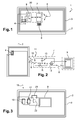
- an electronic radio frequency transaction device 1 is in the example in the form of a chip card or integrated circuit chip support although other embodiments can implement the means of the invention such that a USB stick or any other portable object.
- the card comprises, in known manner, a support or card body 2 comprising an electromagnetic antenna 3 in the plane of the support. This antenna is connected to the terminals of an integrated circuit chip or to those of an electronic module or electronic component 4 having it.
- the chip is capable of implementing at least one software application stored therein to carry out an electronic transaction such as a bank payment, a debit / credit transaction of points, units, loyalty, access control, authentication, etc.
- the application can be implemented by interaction with a radio frequency reader or terminal or another device of the same kind as the invention comprising a function of the NFC (Near Field Communication) type.
- the device also comprises a first switch 6 adapted to allow a radio frequency operation of the device on actuation of the switch and a stop operation after release of the actuation.
- the switch is here open at rest and interrupts a circuit of the device.
- the device comprises a circuit 7 adapted to maintain after activation of the first switch 6, a continuous radiofrequency operation for a predetermined period.
- the circuit 7 capable of maintaining a continuous radiofrequency operation after activation and release of the first is said timer. It is in fact a circuit for maintaining the operation of the antenna regardless of its shape; this circuit is independent of the state of the switch after actuation.
- the duration may be that corresponding to the time during which the device is put in the field after actuation of the main switch.
- Other equivalent circuits may be suitable, such as relay or timer type.
- bistable type circuit whose actuated position operating the device would be maintained as the device is in the electromagnetic field thanks to a particular coil.
- the timer circuit here interrupted by the switch 6 at rest, is also connected on the one hand to a second switch 8 (the switch 8 can also be included in the timer circuit) and on the other hand to a source of power supply or a means of collecting energy 9.
- a source of power supply or a means of collecting energy 9. In the example, it is an electromagnetic field coil 9; It will serve as a current generator under the effect of an electromagnetic field of a reader (not shown).
- the source (or the means 9) can be formed (or be replaced) also by a specific thin battery, in particular of the type used in smart cards or capable of being laminated or embedded in the support or inlay (under -supporting support of an electrical and / or electronic circuit)
- the fixed term corresponds, for example, to at least that required to complete a transaction considered.
- the duration is preferably adjusted to the manufacture or according to the choice of components.
- the timer circuit comprises or actuates a second switch (8, 10, 11) arranged on a main antenna circuit 3;
- this second switch is an electronic switch of the static type; in particular, it is a transistor 8 LED 10 acting on the basis of a transistor 8 to turn it on.
- the timer circuit is able to present an activation state in which this second switch (in particular transistor 8) is actuated to close this main antenna circuit 3.
- the first switch 6 has been connected to connect the energy collection means (here the coil) to the timer circuit 7.
- the energy collection means here the coil
- the timer circuit 7 comprises a rectifier circuit 12 and a capacitor 13 connected to provide an activation threshold voltage of the second switch and a charging voltage of a capacitor 13 on actuation of the first switch 6.
- the capacity of the timer circuit is determined so as to provide by discharge at least one activation threshold voltage of the second switch for at least one time corresponding to a radio frequency transaction.
- the duration (D) may vary depending on the length of the communication exchange from one thousandth of a second to 2 seconds, or even four. banking application, the duration D mini is for example equal to a maximum duration necessary for a transaction type EMV.
- the timer circuit has been arranged and the second the electronic switch in a second module or electronic component 20.
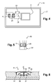
- the radiofrequency device 1 is embodied as an insert or "inlay" 15 for a contactless smart card, obtained according to a particular embodiment.
- the antenna 3 is made on a substrate or support 2 in the form of a closed circuit (with the exception of the antenna ends intended to be connected to the electronic component 3).
- the coil 9 is made on the same substrate.
- the substrate preferably comprises two cavities 16, 17, preferably made before the antenna and coil, for respectively receiving a first module 4 or an integrated circuit chip and the second module or electronic component 20 comprising the timer circuit and, if appropriate, also the second electronic switch.
- the antenna wire and / or coil 9 is embedded in a polymeric support 11 by ultrasound.
- the wires fly over the cavities and module connection locations until they reach a cavity edge.
- Antenna turns and coils could be made otherwise, by any known technique, such as etching and electrochemical deposition, metal sheet cutting, screen printing, embroidery.
- the support may be in various materials including synthetic and / or include fibers of cellulosic material such as paper.
- the coil 9 may be in closed circuit at least momentarily during manufacture and / or customization at a zone 22 receiving or able to receive a switch thereafter.
- a short-circuit element in particular a fuse 23, can be arranged on the coil circuit 9 so as to short-circuit the switch or terminals intended to connect a switch, the element being able to be open in a later step.
- the fuse is placed here just before the switch location but could be placed any way from the moment the switch is short-circuited by the fuse, for example just after.
- the fuse material and its dimensional characteristics are determined to snap the fuse by subjecting the antenna to an electromagnetic field strong enough to generate a breakdown current or intensity.
- the dashed circle 22 illustrates a zone location 2 for receiving the first switch or being machined.
- the first switch is intended to be disposed on the coil circuit.
- the two electronic modules or components 4, 20 are placed on the substrate before or after the realization of the antenna and coil and connected together and to the coil and antenna according to the electrical diagram of the Figures 2 or 3 .
- this transponder substrate provided with switches 6, 8 is covered with at least one sheet or layer of material (not shown) to form an "inlay" or subset said insert.
- the sheet may comprise beforehand a cavity 24 corresponding to the zone 22 intended to receive a switch 6 produced in accordance with FIG. figure 6 for example.
- the figure 6 discloses a switch button 6 in which the turns of the coil 30, 32 are not severed by a housing cavity of a contactor 29, here constituted by a dome comprising in the center a spring housed partly in a mini central cavity of the 24.
- the contactor element 29 is here a Belleville washer, having a central dome possibly connected to four feet (not shown) in the form of an elastic tongue.
- a flexible cover or membrane 52 accessible from the outside, is fixed, in particular by gluing, on a plane 54 machined above the conductive element, by closing the cavity.
- the layer or sheet comprising the switch 6 is preferably made of two sheets or layers, the antenna and / or coil being at their interface.
- the two components or module 4, 20 are arranged in a single module or electronic component 50.
- the module may comprise, for example, a dielectric substrate metallized 51 and locations of the integrated circuit 4 and a location of the component 20 forming or having the timer circuit and electronic or optoelectronic switch. This facilitates the integration and connection of the module in the device during manufacture.
- provision may be made to produce the antenna 3 and / or the coil 9 in the integrated circuit 4 or on the support 2 or on a dielectric 51 of module 50.
- a user approaches his bank card 1 in front of a banking terminal having a radio frequency reader function. After having entered his PIN code on a keypad of the terminal, the user validates the transaction, in particular following a mutual authentication step, by putting his card in the reader's field and by creating a pulse (I) on the first one. switch 6.
- the rectifier bridge of the Wheatstone bridge type 12 provides a DC voltage which feeds directly the emitting diode LED 8 of the switch component, the latter going into a state of conduction and closure of the circuit of the main antenna.
- the main antenna being operational, can itself receive energy from the field of the reader to feed the integrated circuit and initiate a transaction, in particular by retro-modulating the received field.
- the current or voltage induced in the coil has also charged the capacitance 13 placed across the assembly composed of the diode (LED) and resistor (R).
- the user can release the first switch 6 since the capacity 13 by discharging feeds in turn the diode 10 to keep closed the antenna circuit 3.
- a diode can be placed just after the bridge 12 or on the element "shunt" of the resistor and diode.
- the transaction can be advantageously continued without having to maintain the switch actuated further through the invention, as long as the capacity provides a higher voltage at a threshold voltage (TS) necessary for actuation of the electronic switch.
- TS threshold voltage
- the device can also represent an identity document, electronic passport or be included in it.
Priority Applications (6)
| Application Number | Priority Date | Filing Date | Title |
|---|---|---|---|
| EP07301502A EP2053546A1 (de) | 2007-10-26 | 2007-10-26 | Funkkommunikationsvorrichtung, die einen Zeitgeber umfasst |
| PCT/EP2008/063105 WO2009053225A1 (fr) | 2007-10-26 | 2008-09-30 | Dispositif de communication radiofréquence comprenant un temporisateur |
| EP08804931A EP2218040B1 (de) | 2007-10-26 | 2008-09-30 | Hochfrequenzkommunikationseinrichtung mit einem timer |
| ES08804931T ES2377513T3 (es) | 2007-10-26 | 2008-09-30 | Dispositivo de comunicación radiofrecuencia que incluye un temporizador. |
| AT08804931T ATE533121T1 (de) | 2007-10-26 | 2008-09-30 | Hochfrequenzkommunikationseinrichtung mit einem timer |
| US12/739,562 US20100308976A1 (en) | 2007-10-26 | 2008-09-30 | Radiofrequency communication device including a timer |
Applications Claiming Priority (1)
| Application Number | Priority Date | Filing Date | Title |
|---|---|---|---|
| EP07301502A EP2053546A1 (de) | 2007-10-26 | 2007-10-26 | Funkkommunikationsvorrichtung, die einen Zeitgeber umfasst |
Publications (1)
| Publication Number | Publication Date |
|---|---|
| EP2053546A1 true EP2053546A1 (de) | 2009-04-29 |
Family
ID=39200028
Family Applications (2)
| Application Number | Title | Priority Date | Filing Date |
|---|---|---|---|
| EP07301502A Withdrawn EP2053546A1 (de) | 2007-10-26 | 2007-10-26 | Funkkommunikationsvorrichtung, die einen Zeitgeber umfasst |
| EP08804931A Active EP2218040B1 (de) | 2007-10-26 | 2008-09-30 | Hochfrequenzkommunikationseinrichtung mit einem timer |
Family Applications After (1)
| Application Number | Title | Priority Date | Filing Date |
|---|---|---|---|
| EP08804931A Active EP2218040B1 (de) | 2007-10-26 | 2008-09-30 | Hochfrequenzkommunikationseinrichtung mit einem timer |
Country Status (5)
| Country | Link |
|---|---|
| US (1) | US20100308976A1 (de) |
| EP (2) | EP2053546A1 (de) |
| AT (1) | ATE533121T1 (de) |
| ES (1) | ES2377513T3 (de) |
| WO (1) | WO2009053225A1 (de) |
Cited By (3)
| Publication number | Priority date | Publication date | Assignee | Title |
|---|---|---|---|---|
| DE102008052812A1 (de) * | 2008-10-15 | 2010-04-29 | J. Schmalz Gmbh | Unterdruckhandhabungseinrichtung |
| FR2968801A1 (fr) * | 2010-12-10 | 2012-06-15 | St Microelectronics Rousset | Communication sans contact avec autorisation par contact humain |
| WO2015058876A1 (de) * | 2013-10-25 | 2015-04-30 | Bundesdruckerei Gmbh | Dokument mit einer kontaktlosen chipkartenschnittstelle und elektronisches system |
Families Citing this family (15)
| Publication number | Priority date | Publication date | Assignee | Title |
|---|---|---|---|---|
| EP2426627B1 (de) * | 2010-09-02 | 2016-10-12 | Oberthur Technologies | Leuchtmodul für Mikroschaltungsvorrichtung |
| FR2964487B1 (fr) * | 2010-09-02 | 2013-07-12 | Oberthur Technologies | Carte a microcircuit comprenant un moyen lumineux |
| FR2968802B1 (fr) * | 2010-12-10 | 2014-05-23 | St Microelectronics Rousset | Communication sans contact avec autorisation par contact humain et indicateur visuel |
| US9063737B2 (en) | 2012-07-02 | 2015-06-23 | Square, Inc. | Wireless card reader with one or more card interfaces |
| DE102012216472B4 (de) * | 2012-09-14 | 2019-09-05 | Rainer Popp | Vorrichtung zum Senden und Empfangen von Daten |
| US10318952B1 (en) | 2015-05-23 | 2019-06-11 | Square, Inc. | NFC base station and passive transmitter device |
| US10182328B1 (en) | 2015-05-23 | 2019-01-15 | Square, Inc. | Point of sale (POS) device responsive to detected interference with antenna |
| US9936337B2 (en) | 2015-05-23 | 2018-04-03 | Square, Inc. | Tuning a NFC antenna of a device |
| USD766238S1 (en) | 2015-05-29 | 2016-09-13 | Square, Inc. | Card reader |
| USD766901S1 (en) | 2015-05-29 | 2016-09-20 | Square, Inc. | Card reader |
| US10242357B1 (en) | 2015-06-30 | 2019-03-26 | Square, Inc. | Configuration of a payment object reader |
| US10366383B2 (en) | 2016-03-31 | 2019-07-30 | Square, Inc. | Combined reliable and unreliable data transmission |
| US9542678B1 (en) | 2016-03-31 | 2017-01-10 | Square, Inc. | Exclusive bonding of wireless devices |
| AT520415A1 (de) * | 2017-07-20 | 2019-03-15 | Ait Austrian Inst Tech Gmbh | NFC-Transponderanordnung |
| GB2584345B (en) * | 2019-05-31 | 2022-01-12 | Advanced Risc Mach Ltd | Smart labels |
Citations (4)
| Publication number | Priority date | Publication date | Assignee | Title |
|---|---|---|---|---|
| US20030132301A1 (en) * | 2002-12-31 | 2003-07-17 | Massachusetts Institute Of Technology | Manually operated switch for enabling and disabling an RFID card |
| US20070132590A1 (en) * | 2003-12-19 | 2007-06-14 | Wataru Hattori | Id tag |
| WO2007074011A1 (de) * | 2005-12-27 | 2007-07-05 | Bundesdruckerei Gmbh | Dokument mit einem datenspeicher, vorrichtung und verfahren zum lesen eines funketiketts und computerprogrammprodukt |
| DE102006015782A1 (de) * | 2006-04-04 | 2007-10-18 | Infineon Technologies Ag | Vorrichtung zur Speicherung und drahtlosen Übertragung von Daten |
Family Cites Families (50)
| Publication number | Priority date | Publication date | Assignee | Title |
|---|---|---|---|---|
| US358525A (en) * | 1887-03-01 | Fountain-pen | ||
| US4114151A (en) * | 1976-09-14 | 1978-09-12 | Alfa-Laval Company Limited | Passive transponder apparatus for use in an interrogator-responder system |
| US4500795A (en) * | 1982-09-30 | 1985-02-19 | Hochstein Peter A | Electrical timing control switch |
| GB2222714A (en) * | 1988-09-09 | 1990-03-14 | Avery Ltd W & T | Cashless payment system |
| US5318596A (en) * | 1991-11-13 | 1994-06-07 | Exonic Corporation | Activity sensing pacemaker |
| JP3226778B2 (ja) * | 1996-02-06 | 2001-11-05 | 日本電気エンジニアリング株式会社 | バッテリー内蔵型ワイヤレスid装置及びid質問装置 |
| AU4769697A (en) * | 1997-11-07 | 1999-05-31 | Swisscom Ag | Method, system and devices for authenticating persons |
| DE19846803C1 (de) * | 1998-10-10 | 2000-09-07 | Daimler Chrysler Ag | Verfahren zur Herstellung der Zugangsberechtigung zu einem motorangetriebenen Fahrzeug |
| US6219952B1 (en) * | 1999-01-25 | 2001-04-24 | Jonathan E. Mossberg | Magnetic tag firearm safety enhancement system |
| DE60042139D1 (de) * | 1999-02-19 | 2009-06-18 | Nippon Telegraph & Telephone | Kontaktlose Chipkarte und System hierfür |
| NO311713B1 (no) * | 2000-03-22 | 2002-01-14 | Stig Ovar Keller | Fellingskjemikalie samt fremgangsmåte ved, og anvendelse av, fellingskjemikaliet |
| US6952167B2 (en) * | 2000-08-15 | 2005-10-04 | Omron Corporation | Noncontact communication medium and noncontact communication system |
| US7290709B2 (en) * | 2001-04-10 | 2007-11-06 | Erica Tsai | Information card system |
| US6618022B2 (en) * | 2001-07-20 | 2003-09-09 | Delta Systems, Inc. | Radio frequency powered switch |
| US6830193B2 (en) * | 2001-11-29 | 2004-12-14 | Matsushita Electric Industrial Co., Ltd. | Non-contact IC card |
| FR2834367B1 (fr) * | 2001-12-28 | 2005-06-24 | A S K | Objet portable sans contact comportant au moins un dispositif peripherique connecte a la meme antenne que la puce |
| US20030156501A1 (en) * | 2002-01-14 | 2003-08-21 | Martin Spindel | Trackable storage unit system and method |
| JP3920196B2 (ja) * | 2002-11-11 | 2007-05-30 | 松下電器産業株式会社 | 携帯無線装置 |
| US7100835B2 (en) * | 2002-12-31 | 2006-09-05 | Massachusetts Institute Of Technology | Methods and apparatus for wireless RFID cardholder signature and data entry |
| US7898387B2 (en) * | 2003-01-22 | 2011-03-01 | Chrysler Group Llc | Portable remote transmitter to remotely control a vehicle function |
| US7283644B2 (en) * | 2003-06-27 | 2007-10-16 | International Business Machines Corporation | System and method for enhancing security applications |
| US7446646B2 (en) * | 2003-06-30 | 2008-11-04 | Nokia Corporation | System and method for supporting multiple reader-tag configurations using multi-mode radio frequency tag |
| US7347382B2 (en) * | 2004-02-06 | 2008-03-25 | T-Ink, Llc | System for securing personal cards |
| US7132946B2 (en) * | 2004-04-08 | 2006-11-07 | 3M Innovative Properties Company | Variable frequency radio frequency identification (RFID) tags |
| US7151455B2 (en) * | 2004-04-30 | 2006-12-19 | Kimberly-Clark Worldwide, Inc. | Activating a data tag by load or orientation or user control |
| JP4887627B2 (ja) * | 2005-01-19 | 2012-02-29 | 日本電気株式会社 | Rfid読み出しシステム、rfid読み出し方法、rfidリーダ、rfid読み出し管理装置、rfidリーダの制御プログラム及びこれを記録したコンピュータが読み取り可能な情報記録媒体並びにrfid読み出し管理装置の制御プログラム及びこれを記録したコンピュータが読み取り可能な情報記録媒体 |
| US20150254483A1 (en) * | 2005-02-07 | 2015-09-10 | Steven Michael Colby | RFID Sensor |
| JP4595614B2 (ja) * | 2005-03-25 | 2010-12-08 | 株式会社デンソー | 車両ドア制御システム |
| CA2612377C (en) * | 2005-06-16 | 2014-08-12 | Visa International Service Association | Contactless activation systems and methods |
| WO2007012031A2 (en) * | 2005-07-19 | 2007-01-25 | Precision Dynamics Corporation | Semi-active rfid tag and related processes |
| FR2895822B1 (fr) * | 2005-12-29 | 2008-02-15 | Srett Soc Par Actions Simplifi | Procede et dispositif de communication radiofrequence |
| US8331549B2 (en) * | 2006-05-01 | 2012-12-11 | Verint Americas Inc. | System and method for integrated workforce and quality management |
| US20080028230A1 (en) * | 2006-05-05 | 2008-01-31 | Tri-D Systems, Inc. | Biometric authentication proximity card |
| FR2901426B1 (fr) * | 2006-05-19 | 2008-09-12 | Schneider Electric Ind Sas | Dispositif de surveillance de position d'une partie mobile d'un appareil electrique interrupteur |
| US8132026B2 (en) * | 2006-06-02 | 2012-03-06 | Semiconductor Energy Laboratory Co., Ltd. | Power storage device and mobile electronic device having the same |
| US20080016709A1 (en) * | 2006-07-24 | 2008-01-24 | Sperry Michael J | Illuminated bow sight apparatus |
| JP4650456B2 (ja) * | 2006-08-25 | 2011-03-16 | 日立化成工業株式会社 | 回路接続材料、これを用いた回路部材の接続構造及びその製造方法 |
| US7762471B2 (en) * | 2006-09-07 | 2010-07-27 | Mastercard International, Inc. | Proximity payment card with cost-effective connection between user-actuatable input switch and RFID IC |
| US7839124B2 (en) * | 2006-09-29 | 2010-11-23 | Semiconductor Energy Laboratory Co., Ltd. | Wireless power storage device comprising battery, semiconductor device including battery, and method for operating the wireless power storage device |
| US7609165B2 (en) * | 2006-10-27 | 2009-10-27 | Tyco Safety Products Canada Ltd. | Method and apparatus for magnetically activated radio or infrared identification system |
| US7533826B2 (en) * | 2007-02-13 | 2009-05-19 | Mastercard International, Inc. | Electronic wallet |
| US8537055B2 (en) * | 2007-02-27 | 2013-09-17 | Kyocera Corporation | Portable electronic device and magnetic antenna circuit |
| KR101319549B1 (ko) * | 2007-07-16 | 2013-10-21 | 삼성전자주식회사 | 오디오 데이터 송수신방법 및 이 방법을 이용한 전자장치 |
| US20090221232A1 (en) * | 2008-02-29 | 2009-09-03 | Estevez Leonardo W | Portable Telephone With Unitary Transceiver Having Cellular and RFID Functionality |
| US7994920B2 (en) * | 2008-11-14 | 2011-08-09 | International Business Machines Corporation | RFID security in an RFID-enabled medium |
| JP5592613B2 (ja) * | 2009-01-22 | 2014-09-17 | パナソニック株式会社 | 電源装置及びそれを用いた照明器具 |
| US8784189B2 (en) * | 2009-06-08 | 2014-07-22 | Cfph, Llc | Interprocess communication regarding movement of game devices |
| US8648721B2 (en) * | 2010-08-09 | 2014-02-11 | Tyco Fire & Security Gmbh | Security tag with integrated EAS and energy harvesting magnetic element |
| WO2015049973A1 (ja) * | 2013-10-01 | 2015-04-09 | Necトーキン株式会社 | 通信装置 |
| RU2706423C2 (ru) * | 2014-04-25 | 2019-11-19 | Филипс Лайтинг Холдинг Б.В. | Драйвер импульсного источника питания, объединенный с антенной для передачи мощности |
-
2007
- 2007-10-26 EP EP07301502A patent/EP2053546A1/de not_active Withdrawn
-
2008
- 2008-09-30 ES ES08804931T patent/ES2377513T3/es active Active
- 2008-09-30 US US12/739,562 patent/US20100308976A1/en not_active Abandoned
- 2008-09-30 WO PCT/EP2008/063105 patent/WO2009053225A1/fr active Application Filing
- 2008-09-30 AT AT08804931T patent/ATE533121T1/de active
- 2008-09-30 EP EP08804931A patent/EP2218040B1/de active Active
Patent Citations (4)
| Publication number | Priority date | Publication date | Assignee | Title |
|---|---|---|---|---|
| US20030132301A1 (en) * | 2002-12-31 | 2003-07-17 | Massachusetts Institute Of Technology | Manually operated switch for enabling and disabling an RFID card |
| US20070132590A1 (en) * | 2003-12-19 | 2007-06-14 | Wataru Hattori | Id tag |
| WO2007074011A1 (de) * | 2005-12-27 | 2007-07-05 | Bundesdruckerei Gmbh | Dokument mit einem datenspeicher, vorrichtung und verfahren zum lesen eines funketiketts und computerprogrammprodukt |
| DE102006015782A1 (de) * | 2006-04-04 | 2007-10-18 | Infineon Technologies Ag | Vorrichtung zur Speicherung und drahtlosen Übertragung von Daten |
Cited By (4)
| Publication number | Priority date | Publication date | Assignee | Title |
|---|---|---|---|---|
| DE102008052812A1 (de) * | 2008-10-15 | 2010-04-29 | J. Schmalz Gmbh | Unterdruckhandhabungseinrichtung |
| DE102008052812B4 (de) * | 2008-10-15 | 2010-07-08 | J. Schmalz Gmbh | Unterdruckhandhabungseinrichtung |
| FR2968801A1 (fr) * | 2010-12-10 | 2012-06-15 | St Microelectronics Rousset | Communication sans contact avec autorisation par contact humain |
| WO2015058876A1 (de) * | 2013-10-25 | 2015-04-30 | Bundesdruckerei Gmbh | Dokument mit einer kontaktlosen chipkartenschnittstelle und elektronisches system |
Also Published As
| Publication number | Publication date |
|---|---|
| EP2218040A1 (de) | 2010-08-18 |
| US20100308976A1 (en) | 2010-12-09 |
| EP2218040B1 (de) | 2011-11-09 |
| WO2009053225A1 (fr) | 2009-04-30 |
| ES2377513T3 (es) | 2012-03-28 |
| ATE533121T1 (de) | 2011-11-15 |
Similar Documents
| Publication | Publication Date | Title |
|---|---|---|
| EP2218040B1 (de) | Hochfrequenzkommunikationseinrichtung mit einem timer | |
| EP1692642B1 (de) | Sicherheitsdokument mit einem kontaktlosen chip mit datenmaskierung | |
| EP1068590B1 (de) | Kontaklose ic karte mit sperrmitteln | |
| EP2194491A1 (de) | Elektronische Karte, die Steuermittel umfasst | |
| EP1116179B1 (de) | Kontaktlose chipkarte mit hemmungsmitteln | |
| EP2780867A1 (de) | Hochfrequenzkommunikationsvorrichtung mit durch beliebige gesten des trägers gesteuertem betrieb | |
| EP2132683A1 (de) | Verfahren zum herstellen von hochfrequenz-kommunikationsgeräten mit oder ohne betriebsschalter und so erhaltene geräte | |
| EP3343450A1 (de) | Tragbarer gegenstand, der eine nahfeldverbindungsvorrichtung umfasst | |
| EP2182473B1 (de) | Elektronische Vorrichtung, die kontaktlose Kommunikationen im Nahfeld autorisiert | |
| EP2085987B1 (de) | Steuerungsvorrichtung mit zwei verschiedenen Betätigungsarten | |
| WO1997041578A1 (fr) | Carte a circuit integre de faible epaisseur comportant un commutateur perfectionne a actionnement manuel | |
| WO2016131682A1 (fr) | Procede de fabrication d'un module electronique simple face comprenant des zones d'interconnexion | |
| EP2419865B1 (de) | Kommunikationsvorrichtung mit zwei über eine gemeinsame kommunikationsschnittstelle verbundenen chips | |
| EP0714076A1 (de) | Tragbarer Gegenstand mit einer elektronischen Schaltung, betrieben durch eine innere Batterie und mit einem Datenspeicher, Verfahren und Vorrichtung zur äusserlichen Speisung dieses Gegenstandes und Datenübertragung mit letzterem | |
| WO2017191373A1 (fr) | Module électronique de taille réduite pour carte à puce | |
| EP3391293A1 (de) | Verfahren zur herstellung einer vorrichtung mit einem hochfrequenzelektronikmodul und einem indikator | |
| WO2009053224A1 (fr) | Procédé de réalisation de dispositifs de communication radiofréquence comprenant un interrupteur provisoirement en court-circuit | |
| EP2631849A1 (de) | Verfahren zur Herstellung einer Vorrichtung, die ein mit einem elektrischen und/oder elektronischen Schaltkreis ausgestattetes Modul umfasst | |
| WO2014060290A1 (fr) | Procede de fabrication d'un dispositif multi-composants comprenant un module electrique et/ou electronique | |
| FR3003672B1 (fr) | Carte a puce a double interface de communication avec carte micro sd incorporee | |
| EP2242007A2 (de) | Elektronische Vorrichtung, die eine Karte mit Mikroschaltung und eine Hilfsbatterie umfasst | |
| FR3053541A1 (fr) | Entite electronique comportant un transducteur | |
| FR2944631A1 (fr) | Dispositif electronique a microcircuit comprenant une carte a microcircuit et une batterie d'alimentaire de la carte. | |
| EP1788472A1 (de) | Vorrichtung oder Gruppe von Vorrichtungen mit zwei auf verschiedene Frequenzen abgestimmten Antennen |
Legal Events
| Date | Code | Title | Description |
|---|---|---|---|
| PUAI | Public reference made under article 153(3) epc to a published international application that has entered the european phase |
Free format text: ORIGINAL CODE: 0009012 |
|
| AK | Designated contracting states |
Kind code of ref document: A1 Designated state(s): AT BE BG CH CY CZ DE DK EE ES FI FR GB GR HU IE IS IT LI LT LU LV MC MT NL PL PT RO SE SI SK TR |
|
| AX | Request for extension of the european patent |
Extension state: AL BA HR MK RS |
|
| 17P | Request for examination filed |
Effective date: 20091029 |
|
| 17Q | First examination report despatched |
Effective date: 20091203 |
|
| AKX | Designation fees paid |
Designated state(s): AT BE BG CH CY CZ DE DK EE ES FI FR GB GR HU IE IS IT LI LT LU LV MC MT NL PL PT RO SE SI SK TR |
|
| STAA | Information on the status of an ep patent application or granted ep patent |
Free format text: STATUS: THE APPLICATION IS DEEMED TO BE WITHDRAWN |
|
| 18D | Application deemed to be withdrawn |
Effective date: 20100414 |