EP2051304A1 - Semiconductor substrate, method for forming electrode, and method for manufacturing solar cell - Google Patents
Semiconductor substrate, method for forming electrode, and method for manufacturing solar cell Download PDFInfo
- Publication number
- EP2051304A1 EP2051304A1 EP07790675A EP07790675A EP2051304A1 EP 2051304 A1 EP2051304 A1 EP 2051304A1 EP 07790675 A EP07790675 A EP 07790675A EP 07790675 A EP07790675 A EP 07790675A EP 2051304 A1 EP2051304 A1 EP 2051304A1
- Authority
- EP
- European Patent Office
- Prior art keywords
- electrode
- layer
- semiconductor substrate
- electrode layer
- additive
- Prior art date
- Legal status (The legal status is an assumption and is not a legal conclusion. Google has not performed a legal analysis and makes no representation as to the accuracy of the status listed.)
- Granted
Links
Images

Classifications
-
- H—ELECTRICITY
- H10—SEMICONDUCTOR DEVICES; ELECTRIC SOLID-STATE DEVICES NOT OTHERWISE PROVIDED FOR
- H10F—INORGANIC SEMICONDUCTOR DEVICES SENSITIVE TO INFRARED RADIATION, LIGHT, ELECTROMAGNETIC RADIATION OF SHORTER WAVELENGTH OR CORPUSCULAR RADIATION
- H10F77/00—Constructional details of devices covered by this subclass
- H10F77/20—Electrodes
-
- H—ELECTRICITY
- H10—SEMICONDUCTOR DEVICES; ELECTRIC SOLID-STATE DEVICES NOT OTHERWISE PROVIDED FOR
- H10F—INORGANIC SEMICONDUCTOR DEVICES SENSITIVE TO INFRARED RADIATION, LIGHT, ELECTROMAGNETIC RADIATION OF SHORTER WAVELENGTH OR CORPUSCULAR RADIATION
- H10F77/00—Constructional details of devices covered by this subclass
- H10F77/20—Electrodes
- H10F77/206—Electrodes for devices having potential barriers
- H10F77/211—Electrodes for devices having potential barriers for photovoltaic cells
-
- C—CHEMISTRY; METALLURGY
- C03—GLASS; MINERAL OR SLAG WOOL
- C03C—CHEMICAL COMPOSITION OF GLASSES, GLAZES OR VITREOUS ENAMELS; SURFACE TREATMENT OF GLASS; SURFACE TREATMENT OF FIBRES OR FILAMENTS MADE FROM GLASS, MINERALS OR SLAGS; JOINING GLASS TO GLASS OR OTHER MATERIALS
- C03C8/00—Enamels; Glazes; Fusion seal compositions being frit compositions having non-frit additions
- C03C8/14—Glass frit mixtures having non-frit additions, e.g. opacifiers, colorants, mill-additions
-
- C—CHEMISTRY; METALLURGY
- C03—GLASS; MINERAL OR SLAG WOOL
- C03C—CHEMICAL COMPOSITION OF GLASSES, GLAZES OR VITREOUS ENAMELS; SURFACE TREATMENT OF GLASS; SURFACE TREATMENT OF FIBRES OR FILAMENTS MADE FROM GLASS, MINERALS OR SLAGS; JOINING GLASS TO GLASS OR OTHER MATERIALS
- C03C8/00—Enamels; Glazes; Fusion seal compositions being frit compositions having non-frit additions
- C03C8/14—Glass frit mixtures having non-frit additions, e.g. opacifiers, colorants, mill-additions
- C03C8/18—Glass frit mixtures having non-frit additions, e.g. opacifiers, colorants, mill-additions containing free metals
-
- H—ELECTRICITY
- H10—SEMICONDUCTOR DEVICES; ELECTRIC SOLID-STATE DEVICES NOT OTHERWISE PROVIDED FOR
- H10D—INORGANIC ELECTRIC SEMICONDUCTOR DEVICES
- H10D64/00—Electrodes of devices having potential barriers
- H10D64/01—Manufacture or treatment
- H10D64/011—Manufacture or treatment of electrodes ohmically coupled to a semiconductor
-
- H—ELECTRICITY
- H10—SEMICONDUCTOR DEVICES; ELECTRIC SOLID-STATE DEVICES NOT OTHERWISE PROVIDED FOR
- H10F—INORGANIC SEMICONDUCTOR DEVICES SENSITIVE TO INFRARED RADIATION, LIGHT, ELECTROMAGNETIC RADIATION OF SHORTER WAVELENGTH OR CORPUSCULAR RADIATION
- H10F10/00—Individual photovoltaic cells, e.g. solar cells
-
- H—ELECTRICITY
- H10—SEMICONDUCTOR DEVICES; ELECTRIC SOLID-STATE DEVICES NOT OTHERWISE PROVIDED FOR
- H10F—INORGANIC SEMICONDUCTOR DEVICES SENSITIVE TO INFRARED RADIATION, LIGHT, ELECTROMAGNETIC RADIATION OF SHORTER WAVELENGTH OR CORPUSCULAR RADIATION
- H10F19/00—Integrated devices, or assemblies of multiple devices, comprising at least one photovoltaic cell covered by group H10F10/00, e.g. photovoltaic modules
- H10F19/90—Structures for connecting between photovoltaic cells, e.g. interconnections or insulating spacers
-
- H—ELECTRICITY
- H10—SEMICONDUCTOR DEVICES; ELECTRIC SOLID-STATE DEVICES NOT OTHERWISE PROVIDED FOR
- H10P—GENERIC PROCESSES OR APPARATUS FOR THE MANUFACTURE OR TREATMENT OF DEVICES COVERED BY CLASS H10
- H10P32/00—Diffusion of dopants within, into or out of wafers, substrates or parts of devices
- H10P32/10—Diffusion of dopants within, into or out of semiconductor bodies or layers
- H10P32/19—Diffusion sources
-
- H—ELECTRICITY
- H10—SEMICONDUCTOR DEVICES; ELECTRIC SOLID-STATE DEVICES NOT OTHERWISE PROVIDED FOR
- H10W—GENERIC PACKAGES, INTERCONNECTIONS, CONNECTORS OR OTHER CONSTRUCTIONAL DETAILS OF DEVICES COVERED BY CLASS H10
- H10W72/00—Interconnections or connectors in packages
- H10W72/50—Bond wires
- H10W72/531—Shapes of wire connectors
- H10W72/536—Shapes of wire connectors the connected ends being ball-shaped
-
- H—ELECTRICITY
- H10—SEMICONDUCTOR DEVICES; ELECTRIC SOLID-STATE DEVICES NOT OTHERWISE PROVIDED FOR
- H10W—GENERIC PACKAGES, INTERCONNECTIONS, CONNECTORS OR OTHER CONSTRUCTIONAL DETAILS OF DEVICES COVERED BY CLASS H10
- H10W72/00—Interconnections or connectors in packages
- H10W72/851—Dispositions of multiple connectors or interconnections
- H10W72/874—On different surfaces
- H10W72/884—Die-attach connectors and bond wires
-
- Y—GENERAL TAGGING OF NEW TECHNOLOGICAL DEVELOPMENTS; GENERAL TAGGING OF CROSS-SECTIONAL TECHNOLOGIES SPANNING OVER SEVERAL SECTIONS OF THE IPC; TECHNICAL SUBJECTS COVERED BY FORMER USPC CROSS-REFERENCE ART COLLECTIONS [XRACs] AND DIGESTS
- Y02—TECHNOLOGIES OR APPLICATIONS FOR MITIGATION OR ADAPTATION AGAINST CLIMATE CHANGE
- Y02E—REDUCTION OF GREENHOUSE GAS [GHG] EMISSIONS, RELATED TO ENERGY GENERATION, TRANSMISSION OR DISTRIBUTION
- Y02E10/00—Energy generation through renewable energy sources
- Y02E10/50—Photovoltaic [PV] energy
Definitions
- the present invention relates to a semiconductor substrate having an electrode formed thereon; and a method for forming an electrode on a semiconductor substrate, and a method for fabricating a solar cell using it.
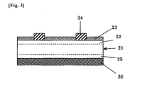
- a structure of a conventional typical solar cell is shown in Fig. 3 . It has a structure in which, on the side of one main surface of a p-type Si substrate 21 formed of single-crystal or polycrystalline Si having a thickness of the order of 0.25 mm, an emitter layer (n + layer) 22 into which P or the like is diffused at a depth of 0.1 to 0.5 ⁇ m is provided, and an antireflection film 23 formed of Si 3 N 4 , SiO 2 , or the like, for reducing the front surface reflectance and a front surface electrode (light receiving surface electrode) 34 for extracting current are formed thereon; on the other side (the side of a back surface) of the Si substrate, a BSF layer (p + layer) 25 into which Al or the like is diffused in high concentration is formed, and, on this back surface, a back surface electrode 26 is formed.
- the front surface electrode 34 is in general formed by the following printing/firing process because of its easiness, low costs, and the like. That is, as a material of the front surface electrode, a conductive paste mixed with a silver powder is in general used; and, after this conductive paste is applied by screen printing or the like, it is sintered at a high temperature in a firing furnace so as to form the front surface electrode.
- a conductive paste containing a silver powder, a glass frit, an organic vehicle, and an organic solvent as the main components is used.
- the contact resistance between the front surface electrode 34 formed by this method and the Si substrate 21 and the wire resistance of the electrode greatly affect the conversion efficiency of the solar cell, and, in order to achieve high efficiency (low cell series resistance, a high fill factor), the contact resistance and the interconnect resistance of the front surface electrode 34 are required to be sufficiently low.
- the glass frit contained in the conductive paste is melted during high-temperature sintering, and part thereof runs down to the interface between the Si substrate and the silver electrode and forms a barrier layer, making it impossible to obtain contact resistance which is low enough to achieve a high-efficiency solar cell.
- the ohmic contact formed by mixing an oxide such as zinc oxide into a conductive paste is improved as the additive amount thereof is increased; however, it tends to hamper sintering of silver when the electrode is fired, leading to an increase in interconnect resistance due to an increase in the specific resistance of the sintered silver product. That is, the problem is that, when the additive amount exceeds a certain level, an improvement of the ohmic contact and the interconnect resistance increasing effect act in an opposing manner, interfering with a significant improvement of the performance of the solar cell as compared with the conventional one.
- Another problem is that its drawback such as a decrease in the adhesive strength between the electrode and a wire caused by the occurrence of so-called silver leaching by which, for soldering to a solder coated ribbon for connection with the solar cell, unsintered silver forms a compound with Sn contained in the solder and disappears in the solder results in a decrease in performance of the solar cell or hinders modularization thereof.
- the present invention has been made in view of the problems described above, and an object thereof is to form, on a semiconductor substrate, an electrode adhered to the semiconductor substrate with sufficient adhesive strength and adhered to a wire via solder with sufficient adhesive strength by lowering both contact resistance and interconnect resistance.
- the present invention has been made to solve the above problems, and provides a semiconductor substrate having at least an electrode formed thereon, in which the electrode has a multilayer structure including two or more layers, of the multilayer structure, at least a first electrode layer directly bonded to the semiconductor substrate contains at least silver and a glass frit, and contains, as an additive, at least one of oxides of Ti, Bi, Zr, V, Nb, Ta, Cr, Mo, W, Mn, Fe, Co, Ni, Si, Al, Ge, Sn, Pb, and Zn, and of an electrode layer formed on the first electrode layer, at least an uppermost electrode layer to be bonded to a wire contains at least silver and a glass frit and does not contain the additive.
- a semiconductor substrate having an electrode having a multilayer structure including two or more layers in which at least a first electrode layer contains silver and a glass frit and contains the above-described additive, and, of an electrode layer formed on the first electrode layer, at least an uppermost electrode layer to be bonded to a wire contains at least silver and a glass frit and does not contain the above-described additive, it is possible to lower the contact resistance between the electrode and the semiconductor substrate while allowing the electrode to be adhered to the semiconductor substrate with sufficient adhesion.
- the content of the additive contained in the at least first electrode layer be 1 wt% or more but less than 15 wt%.
- the content of the additive contained in the at least first electrode layer is 1 wt% or more but less than 15 wt%, it is possible to lower the contact resistance between the electrode and the semiconductor substrate more reliably.
- the semiconductor substrate described above may be configured so that the semiconductor substrate has a pn junction, the electrode is a front surface electrode, on the side of the front surface electrode, an antireflection film is provided, on the side of a back surface, a back surface electrode is provided, and the semiconductor substrate operates as a solar cell.
- the above-described semiconductor substrate operate as a solar cell, it is possible to achieve a high-efficiency solar cell that can form an ohmic contact, has low contact resistance and low interconnect resistance, and has stable characteristics. Moreover, it is possible to achieve a solar cell in which the front surface electrode and the semiconductor substrate adhere to each other with sufficient adhesive strength and the front surface electrode and the wire adhere to each other with sufficient adhesive strength.
- the present invention provides a method for forming an electrode, including: a step of forming a first electrode layer by applying a conductive paste containing at least a silver powder, a glass frit, an organic vehicle, and an organic solvent, and containing, as an additive, at least one of oxides of Ti, Bi, Zr, V, Nb, Ta, Cr, Mo, W, Mn, Fe, Co, Ni, Si, Al, Ge, Sn, Pb, and Zn to a semiconductor substrate, and applying heat; and a step of forming an uppermost electrode layer, which is to be bonded to a wire, by applying, above the first electrode layer, a conductive paste which contains at least a silver powder, a glass frit, an organic vehicle, and an organic solvent and does not contain the additive, and applying heat.
- an electrode including: a step of forming a first electrode layer by applying a conductive paste containing the above-described additive to a semiconductor substrate and applying heat; and a step of forming an uppermost electrode layer, which is to be bonded to a wire, by applying, above the first electrode layer, a conductive paste which does not contain the above-described additive and applying heat, it is possible to form, on a semiconductor substrate, an electrode whose contact resistance with the semiconductor substrate is lowered without decreasing the adhesion of the electrode with the semiconductor substrate.
- the content of the additive contained in the conductive paste forming the at least first electrode layer be 1 wt% or more but less than 15 wt%.
- the content of the additive contained in the conductive paste forming the at least first electrode layer is 1 wt% or more but less than 15 wt%, it is possible to lower the contact resistance with the semiconductor substrate more reliably.
- the present invention provides a method for fabricating a solar cell, including at least: a step of forming an antireflection film on the side of a front surface of a semiconductor substrate having a pn junction; a step of forming a front surface electrode in an antireflection film portion; and a step of forming a back surface electrode on the side of a back surface, in which at least formation of the front surface electrode is performed by the above-described method for forming an electrode.
- the method for fabricating a solar cell including a step of forming an electrode according to the above-described method for forming an electrode, it is possible to fabricate a solar cell having a front surface electrode which has low contact resistance and low interconnect resistance, adheres to the solar cell substrate with sufficient adhesion, and is soldered to the wire with sufficient soldering strength. Then, such a solar cell makes it possible to improve a fill factor, conversion efficiency, and the like.
- the semiconductor substrate according to the present invention it is possible to achieve a semiconductor substrate having an electrode whose contact resistance with the semiconductor substrate and interconnect resistance are both low and which adheres to the semiconductor substrate with sufficient adhesion and is soldered to the wire with sufficient soldering strength.
- the method for forming an electrode according to the present invention it is possible to form, on a semiconductor substrate, an electrode whose contact resistance with the semiconductor substrate and interconnect resistance are both low and which adheres to the semiconductor substrate with sufficient adhesion and is soldered to the wire with sufficient soldering strength.
- there is no need to perform an additional treatment for lowering the contact resistance it is possible to reduce the number of formation steps and realize cost reduction. Then, by applying such methods for forming a semiconductor substrate and an electrode to a solar cell, it is possible to fabricate a high-efficiency and low-cost solar cell.
- the inventors earnestly studied a method for achieving the lowest possible contact resistance of an electrode without performing heat treatment in an atmosphere of hydrogen or immersion in a diluted hydrofluoric acid solution, and for forming an electrode that does not suffer from a silver leaching phenomenon at a junction between the electrode and the wire.
- the inventors have found out that it is possible to make an electrode have low contact resistance at a junction with the semiconductor substrate, have excellent adhesive properties, and suffer less from silver leaching at a junction with the wire by making the electrode have a multilayer structure including two or more layers, adding the above-described additive which is effective in lowering contact resistance to at least a first electrode layer which is directly bonded to the substrate, and not adding such an additive which causes an increase in interconnect resistance and the occurrence of silver leaching to at least the uppermost electrode layer which is bonded to the wire. Then, the inventors conducted additional experiments and studies for the optimization of various conditions, and completed the invention.
- Fig. 1 is a schematic view of a semiconductor substrate 1 according to the invention.
- a semiconductor substrate 11 such as a silicon single crystal substrate, serving as a support substrate
- an electrode 12 is formed, and this electrode 12 has a multilayer structure including two or more layers.
- the multilayer structure of the electrode 12 has formed therein a first electrode layer 13 which is directly bonded to the semiconductor substrate 11, an intermediate electrode layer 14 including a second electrode layer formed directly on the first electrode layer, a third electrode layer formed directly on the second electrode layer, ..., and, as the uppermost layer, an uppermost electrode layer 15.
- the electrode 12 is simply required to include two or more layers; when the electrode 12 includes two layers, it is provided with no intermediate electrode layer 14, and the second electrode layer is formed directly on the first electrode layer 13 as the uppermost electrode layer 15.
- the uppermost electrode layer 15 is bonded to a wire 16 by solder 17.
- the first electrode layer 13 contains at least silver and a glass frit, and contains as an additive at least one of oxides of Ti, Bi, Zr, V, Nb, Ta, Cr, Mo, W, Mn, Fe, Co, Ni, Si, Al, Ge, Sn, Pb, and Zn
- at least the uppermost electrode layer 15 contains at least silver and a glass frit and does not contain the above-described additive.
- the intermediate electrode layer 14 contains at least silver and a glass frit, but may or may not contain the above-described additive.
- An electrode in the semiconductor substrate of the invention having the structure described above can be formed as follows. After the semiconductor substrate 11 serving as the support substrate is prepared, the first electrode layer 13 is first formed on the semiconductor substrate 11. At this time, for a reason, which will be, described later, a thin oxide film, a thin nitride film, or the like, may be formed on the semiconductor substrate 11.
- the formation of the first electrode layer 13 can be performed by applying a conductive paste containing at least a silver powder, a glass frit, an organic vehicle, and an organic solvent, and containing, in addition to them, as an additive, at least one of oxides of Ti, Bi, Zr, V, Nb, Ta, Cr, Mo, W, Mn, Fe, Co, Ni, Si, Al, Ge, Sn, Pb, and Zn to the semiconductor substrate 11, and by heating it at a temperature of 150 to 200°C, for example, so as to vaporize the organic solvent contained in the conductive paste.
- the organic vehicle and the organic solvent it is simply necessary to mix a commonly used organic vehicle and organic solvent.
- the intermediate electrode layer 14 is formed between the first electrode layer 13 and the uppermost electrode layer 15 as follows.
- the intermediate electrode layer 14 can be performed by applying a conductive paste containing at least a silver powder, a glass frit, an organic vehicle, and an organic solvent to the first electrode layer 13, and by heating it at a temperature of 150 to 200°C, for example, so as to vaporize the organic solvent contained in the conductive paste.
- the conductive paste used for forming the intermediate electrode layer 14 may or may not contain the above-described additive, either of which can be chosen appropriately. By repeating the above procedure, one or more electrode layer(s) 14 is formed.
- the uppermost electrode layer 15 is formed.
- the uppermost electrode layer 15 can be performed by applying a conductive paste which contains at least a silver powder, a glass frit, an organic vehicle, and an organic solvent and does not contain the above-described additive to the intermediate electrode layer 14, and by heating it at a temperature of 150 to 200°C, for example, so as to vaporize the organic solvent contained in the conductive paste.
- the electrode 12 includes two layers, although the uppermost electrode layer 15 is formed directly on the first electrode layer 13, it is formed by the same formation method as described above.
- the layers of the electrode 12 are formed as described above, firing is performed at a high temperature of 600 to 850°C, for example, for one to five minutes, for example. As a result of this firing, the organic vehicle contained in the conductive paste of each layer disappears, and the silver in each layer of the electrode is sintered, whereby the electrode 12 is formed.
- the electrode formed on the semiconductor substrate being structured as described above, the following effects are produced. That is, in the first electrode layer 13 directly bonded to the semiconductor substrate 11, due to the above-described additive added thereto, the contact resistance with the semiconductor substrate is low, making it possible to provide an ohmic contact with stability.
- a Ti, Bi, Zr, V, Nb, Ta, Cr, Mo, W, Mn, Fe, Co, Ni, Si, Al, Ge, Sn, Pb, or Zn component in the oxide acts on the glass frit during firing and part thereof merges into it, and, thereafter, the mixture obtained as a result of this merging acts on the oxide film or the like on the semiconductor substrate, contributing to an improvement in contact properties and adhesive strength.
- the glass frit inherently contains oxides of Pb, B, Si, and the like, and can lower the contact resistance between the electrode and the semiconductor substrate; by additionally adding these additives to the electrode layer, it is possible to further lower the contact resistance.
- the uppermost electrode layer 15 bonded to the wire 16 via the solder 17 does not contain the above-described additive.
- sintering of silver is hampered. When sintering of silver is hampered as just described, it becomes a factor that increases the specific resistance of the electrode layer, and, when a contact with the solder is made for connection with the wire, the reaction with Sn in the solder occurs, whereby a so-called silver leaching phenomenon by which it merges into the solder tends to occur.
- the uppermost electrode layer 15 of the electrode 12 formed on the semiconductor substrate according to the invention does not contain the above-described additive, sintering of silver is performed to a satisfactory extent in the process of firing the electrode, making it possible to lower the specific resistance of the electrode layer to a satisfactory level and reduce the occurrence of silver leaching.
- the electrode 12 as a whole can achieve lower contact resistance between the electrode and the semiconductor substrate and lower interconnect resistance, and it is possible to solder the wire to the electrode satisfactorily.
- the electrode 12 when such an electrode is formed, there is no need to perform heat treatment in an atmosphere of hydrogen, immersion in a diluted hydrofluoric acid solution, or the like, it is possible to reduce the number of electrode forming steps and cost.
- the content of the above-described additive added to the first electrode layer 13 be 1 wt% or more but less than 15 wt%.
- the content thereof is made equal to the content above.
- the abovementioned content of the above-described additive in the electrode layer can be largely attained by setting the content of the above-described additive in the conductive paste to 1 wt% or more but less than 15 wt% when the first electrode layer 13 is formed by using the conductive paste. Setting the content of the above-described additive in the electrode layer to such a value is preferable, because this makes it possible to lower the contact resistance between the electrode and the semiconductor substrate more reliably.
- the content of the above-described additive is 1 wt% or more, a contact resistance lowering effect is sufficient.
- the content of the above-described additive is less than 15 wt%, it does not hamper sintering of silver or increase the specific resistance of the electrode, making it possible to obtain a sufficient resistance lowering effect in the semiconductor substrate as a whole including the electrode.
- Such an electrode 12 is suitably applied in particular to a front surface electrode of a solar cell.
- a schematic view of an example of a solar cell according to the invention is shown in Fig. 2 .
- the structure thereof is the same as that of a conventional solar cell except for the front surface electrode.
- the following structure is possible.
- an emitter layer (n + layer) 22 into which P or the like is diffused at a depth of 0.1 to 0.5 ⁇ m is provided, and an antireflection film 23 formed of Si 3 N 4 , SiO 2 , or the like, for reducing the front surface reflectance and a front surface electrode (light receiving surface electrode) 27 for extracting current are formed thereon; on the other side (the side of a back surface) of the Si substrate, a back surface electrode 26 is formed, and a BSF layer (p + layer) 25 into which Al or the like is diffused in high concentration is formed as needed.
- the front surface electrode 27 includes a first electrode layer 27a and a second electrode layer (uppermost electrode layer) 27b, of which the first electrode layer 27a contains at least silver and a glass frit, and contains as an additive at least one of oxides of Ti, Bi, Zr, V, Nb, Ta, Cr, Mo, W, Mn, Fe, Co, Ni, Si, Al, Ge, Sn, Pb, and Zn, and the second electrode layer 27b (uppermost electrode layer) contains at least silver and a glass frit and does not contain the above-described additive.
- Fig. 2 shows a case in which the front surface electrode 27 includes two layers; however, the electrode structure shown in Fig. 1 can be applied to the front surface electrode 27, and it may have an intermediate electrode layer and include three or more electrode layers.
- the example deals with a case in which the semiconductor substrate of the invention is used in the solar cell.
- the invention is not limited thereto, and can be applied to a semiconductor substrate of any type as long as it has an electrode.
- Such a solar cell can be fabricated, for example, as follows.
- the slice damage removal process and texture (irregularities for optical confinement) formation are performed.
- the texture can be easily formed by immersion in a heated alkali solution (concentration: several to several tens percent, temperature: 60 to 100°C) of sodium hydroxide, potassium hydroxide, potassium carbonate, sodium carbonate, sodium acid carbonate, or the like, for about 10 to 30 minutes.
- a predetermined amount of 2-propanol is often dissolved into the above-described solution so as to accelerate a reaction.
- the semiconductor substrate 21 is cleaned in an acid aqueous solution such as hydrochloric acid, sulfuric acid, nitric acid, hydrofluoric acid, or a mixture thereof.
- an acid aqueous solution such as hydrochloric acid, sulfuric acid, nitric acid, hydrofluoric acid, or a mixture thereof.
- cleaning in hydrochloric acid is preferable.
- cleaning may be performed using a hydrochloric acid solution mixed with several percent hydrogen peroxide and heated to 60 to 90°C.
- an emitter layer 22 is formed by a vapor-phase diffusion method using phosphorus oxychloride.
- vapor-phase diffusion be performed in such a way that they are placed on a diffusion board in pairs with the back surfaces thereof brought into contact with each other.
- heating treatment is performed in an atmosphere of phosphorus oxychloride at a temperature of 820 to 880°C for several tens of minutes, whereby an n-type layer is formed on the light receiving surface.
- the depth of the emitter layer thus formed is set at 0.2 to 1.0 ⁇ m, and the sheet resistance is set at 40 to 150 ⁇ / ⁇ .
- the phosphorus glass formed as a result of diffusion is removed by immersion in a several percent hydrofluoric acid solution for several minutes.
- an antireflection film 23 on the front surface is formed.
- the antireflection film 23 not only silicon oxide and silicon nitride, but also cerium oxide, alumina, tin dioxide, titanium dioxide, magnesium fluoride, tantalum oxide, and the like, and a two-layer film obtained by combining two of them are used, and it is possible to use any of them.
- the antireflection film is formed by using PVD, CVD, or the like, and can be formed by any of these methods. In order to fabricate a high-efficiency solar cell, the one formed of silicon nitride by remote plasma CVD is preferable, because it can achieve a low surface recombination rate.
- a back surface electrode 26 is formed on the back surface so as to be 10 to 50 ⁇ m.
- metal such as silver or copper is used, but Al is most preferable in the interests of economy, workability, and contact with silicon. Deposition of the metal layer is possible by any of sputtering, vacuum deposition, screen printing, and the like.
- the metal electrode is uniformly deposited on the back surface.
- the electrode containing Al as the main component by using screen printing is desirable, because firing it allows Al to diffuse into the Si substrate at a junction with the Si substrate, whereby the Si substrate is able to form a back surface electric field region (a BSF layer; a highly-doped p + region) 25 containing a large amount of p-type impurities.
- a front surface electrode 27 of the invention is formed as follows.
- a first electrode layer 27a is formed by, after placing a conductive paste which contains a silver powder, a glass frit, an organic vehicle, and an organic solvent as the main components, and to which the above-described additive is added, and a second electrode layer (in this case, serving as the "uppermost electrode layer") 27b is formed by, after placing a conductive paste which contains a silver powder, a glass frit, an organic vehicle, and an organic solvent as the main components, and does not contain the above-described additive, on the front surface of the antireflection film, drying the organic solvent, and then firing them at a temperature of 600 to 850°C for one to five minutes.
- the antireflection film is melted as a result of heating for firing, and the front surface electrode 27 breaks through the antireflection film and adheres to the semiconductor layer itself of the semiconductor substrate 21 in such a way that the electrode is directly bonded thereto. It is to be noted that the formation of the front surface electrode 27 and the formation of the back surface electrode 26 may be performed in the reverse order.
- Ten solar cells were fabricated by performing the following process for ten semiconductor substrates. First, a boron-doped ⁇ 100 ⁇ p-type as-cut silicon substrate 21 measuring 15 cm per side, having a thickness of 250 ⁇ m, and having a resistivity of 2.0 ⁇ cm was prepared.
- a semiconductor substrate was fabricated by removing a damaged layer by a concentrated potassium hydroxide solution, forming texture, forming an emitter layer 22 subjected to heat treatment in an atmosphere of phosphorus oxychloride at a temperature of 850°C, removing phosphorus glass, forming an antireflection film 23, and forming a back surface electrode 26 by screen printing a paste containing aluminum as the main component all over the back surface and then drying the organic solvent.
- a front surface electrode 27 was formed as follows. First, a conductive paste which contains a silver powder, a glass frit, an organic vehicle, and an organic solvent as the main components and contains 5 wt% ZnO as an additive was applied to the antireflection film formed on the semiconductor substrate by screen printing, and the organic solvent was dried in a 150°C clean oven, whereby a first electrode layer 27a was formed.
- a conductive paste which contains a silver powder, a glass frit, an organic vehicle, and an organic solvent as the main components and does not contain an additive such as ZnO was applied to the first electrode layer, and the organic solvent was dried in a 150°C clean oven, whereby a second electrode layer 27b serving as the uppermost electrode layer was formed.
- the semiconductor substrate having these electrode layers formed thereon was heated in a near-infrared furnace whose maximum temperature was set at 750°C for five minutes, whereby the entire electrode 27 was fired.
- the tensile strength of the electrode portion was measured as a tensile force by attaching copper foil to the electrode portion by soldering and measuring the tensile force with which the copper foil came off or a breakdown of the cell occurred when it was pulled in a vertical direction.
- Electrodes having a front surface electrode with a three-layer structure were fabricated by a method, which is similar to Example 1, but is different therefrom in that electrode layer formation was performed three times as follows. First, a conductive paste which contains a silver powder, a glass frit, an organic vehicle, and an organic solvent as the main components and contains 5 wt% ZnO as an additive was applied, and the organic solvent was dried in a 150°C clean oven, whereby a first electrode layer was formed.
- a conductive paste which contains a silver powder, a glass frit, an organic vehicle, and an organic solvent as the main components and does not contain an additive such as ZnO was applied to the first electrode layer, and the organic solvent was dried in a 150°C clean oven, whereby a second electrode layer was formed.
- a conductive paste which is the same as the conductive paste forming the second electrode layer, that is, which contains a silver powder, a glass frit, an organic vehicle, and an organic solvent as the main components and does not contain an additive such as ZnO was applied to the second electrode layer, and the organic solvent was dried in a 150°C clean oven, whereby a third electrode layer serving as the uppermost electrode layer was formed.
- the semiconductor substrate having these electrode layers formed thereon was heated in a near-infrared furnace whose maximum temperature was set at 750°C for five minutes, whereby the entire electrode was fired.
- characteristic evaluation was conducted and the tensile strength of the electrode was measured as in Example 1.
- Example 3 By a method which is similar to Example 1, but is different therefrom in that a two-layer electrode is formed on the solar cell by using ZnO as an additive added to the first electrode layer 27a and setting the contents thereof at 10 wt% (Example 3), 15 wt% (Example 4), and 20 wt% (Example 5), ten solar cells were fabricated for each case. For the ten solar cells fabricated in the manner as described above, characteristic evaluation was conducted and the tensile strength of the electrode was measured as in Example 1.
- a front surface electrode 34 was formed by applying a conductive paste which contains a silver powder, a glass frit, an organic vehicle, and an organic solvent as the main components and does not contain an additive such as ZnO, and drying the organic solvent in a 150°C clean oven, and then it was heated in a near-infrared furnace whose maximum temperature was set at 750°C for five minutes, whereby the front surface electrode 34 was fired.
- Example 1 For the ten solar cells fabricated in the manner as described above, characteristic evaluation was conducted and the tensile strength of the electrode was measured as in Example 1 (measurement (a)). In addition, after the measurement (a), immersion in a diluted hydrofluoric acid solution was performed for 20 seconds. For the ten solar cells subjected to such treatment, characteristic evaluation was conducted again and the tensile strength of the electrode was measured again as in Example 1 (measurement (b)).
- a front surface electrode 34 was formed by applying a conductive paste which contains a silver powder, a glass frit, an organic vehicle, and an organic solvent as the main components and contains 5 w% ZnO as an additive, and drying the organic solvent in a 150°C clean oven, and then it was heated in a near-infrared furnace whose maximum temperature was set at 750°C for five minutes, whereby the front surface electrode 34 was fired.
- a conductive paste which contains a silver powder, a glass frit, an organic vehicle, and an organic solvent as the main components and contains 5 w% ZnO as an additive
- Example 1 Ten solar cells were fabricated just like Example 1 except that ZnO was added to the first electrode layer 27a as an additive thereof and the content thereof was kept at 5 wt%, and ZnO was added to the second electrode layer 27b as an additive thereof and the content thereof was set at 5 wt%, whereby a two-layer electrode was formed on the solar cell.
- characteristic evaluation was conducted and the tensile strength of the electrode was measured as in Example 1.
- Example 1 shows the average measured values of electrical characteristics of the ten solar cells of each case
- Table 2 shows the average measured values of the tensile strength of the ten solar cells of each case.
- Comparative Example 1 the results of the measurements (a) and (b) are shown as Comparative Example 1(a) and Comparative Example 1(b), respectively.
- Comparative Example 2 in which it contains ZnO, achieves a higher fill factor with lowering contact resistance of the solar cell and achieves higher conversion efficiency, as compared with Comparative Example 1(a), in which the first electrode layer directly formed on the substrate does not contain ZnO.
- Comparative Example 2 which is provided with a single-layer electrode
- the solar cells of Comparative Example 3 and Examples 1 to 5 in which the electrodes each include two or more layers, achieve much higher fill factors and higher conversion efficiencies.
- the solar cells of Examples 1 to 5 achieve much higher fill factors and higher conversion efficiencies, as compared with Comparative Example 3, in which the second electrode layer contains ZnO. This is because ZnO contained in the electrode increases the specific resistance of the electrode, which is the sintered silver product, resulting in an increase in interconnect resistance of the electrode. This is apparent from a comparison between Comparative Example 1(a) and Comparative Example 2.
- Example 5 has a lower fill factor of the solar cell and lower conversion efficiency, as compared with Examples 1 to 4.
- the reason is considered as follows: although the second electrode layer does not contain ZnO, the first electrode layer contains excessive ZnO, leading to an increase in interconnect resistance of the electrode.
- Comparative Example 1(b) which is obtained by dipping Comparative Example 1(a), in which the electrode directly formed on the substrate does not contain ZnO, into a 5% diluted hydrofluoric acid solution for 20 seconds, achieves a higher fill factor and higher conversion efficiency as compared with Comparative Example 2, in which it contains ZnO.
- the electrode tensile strength measurement results shown in Table 2 have revealed the following.
- the tensile strengths of Comparative Examples 2 and 3 irrespective of a single-layer structure or a multilayer structure, in which the electrode layer serving as a joint area for soldering contains ZnO, are low.
- Comparative Example 1(b) which has the electrode containing no ZnO but is subjected to treatment with diluted hydrofluoric acid, restores conversion efficiency as described above, the tensile strength thereof is decreased, making it impracticable.
- the solar cells of Examples 1 to 5, in particular of Examples 1 to 4 are found to have good electrical characteristics and high tensile strength, and the effectiveness of the invention has been verified.
- Example 6 By a method which is similar to Example 1, but is different therefrom in that a two-layer electrode is formed on the solar cell by using TiO 2 as an additive added to the first electrode layer 27a and setting the contents thereof at 5 wt% (Example 6), 15 wt% (Example 7), and 20 wt% (Example 8), ten solar cells were fabricated for each case. In addition, ten solar cells were fabricated just like Comparative Example 2 except that TiO 2 was added to the front surface electrode 34 as an additive thereof, and the front surface electrode had a single-layer structure (Comparative Example 4).
- Example 9 By a method which is similar to Example 1, but is different therefrom in that a two-layer electrode is formed on the solar cell by using Bi 2 O 3 as an additive added to the first electrode layer 27a and setting the contents thereof at 5 wt% (Example 9), 15 wt% (Example 10), and 20 wt% (Example 11), ten solar cells were fabricated for each case.
- ten solar cells were fabricated just like Comparative Example 2 except that Bi 2 O 3 was added to the front surface electrode 34 as an additive thereof, and the front surface electrode had a single-layer structure (Comparative Example 5).
- Example 12 By a method which is similar to Example 1, but is different therefrom in that a two-layer electrode is formed on the solar cell by using PbO as an additive added to the first electrode layer 27a and setting the contents thereof at 5 wt% (Example 12), 15 wt% (Example 13), and 20 wt% (Example 14), ten solar cells were fabricated for each case. In addition, ten solar cells were fabricated just like Comparative Example 2 except that PbO was added to the front surface electrode 34 as an additive thereof, and the front surface electrode had a single-layer structure (Comparative Example 6).
- Example 1 For the ten solar cells of each case fabricated in the manner as described above, characteristic evaluation was conducted and the tensile strength of the electrode was measured as in Example 1. As is the case of ZnO, the characteristic evaluation and electrode tensile strength measurement results of Examples 6 to 8 and Comparative Example 4 (Tables 3 and 4), Examples 9 to 11 and Comparative Example 5 (Tables 5 and 6), and Examples 12 to 14 and Comparative Example 6 (Tables 7 and 8) are shown in Tables 3 to 8 below. The value in the table indicates the average value of the ten solar cells of each case.
- the electrode tensile strength measurement results as for the strength of the copper foil attached to the electrode portion by soldering, the tensile strengths of Comparative Examples 4, 5, and 6 in which the electrode has a single-layer structure and the electrode layer serving as a joint area for soldering contains an additive are low.
- the solar cells obtained by adding an additive to the second electrode layer (Examples 6 to 14), in particular, by setting the additive content at 5 wt% or 15 wt% (Examples 6, 7, 9, 10, 12, and 13) are found to have good electrical characteristics and high tensile strength. Thus the effectiveness of the invention has been verified.
Landscapes
- Chemical & Material Sciences (AREA)
- Life Sciences & Earth Sciences (AREA)
- Engineering & Computer Science (AREA)
- Chemical Kinetics & Catalysis (AREA)
- General Chemical & Material Sciences (AREA)
- Geochemistry & Mineralogy (AREA)
- Materials Engineering (AREA)
- Organic Chemistry (AREA)
- Photovoltaic Devices (AREA)
- Electrodes Of Semiconductors (AREA)
- Conductive Materials (AREA)
Abstract
Description
- The present invention relates to a semiconductor substrate having an electrode formed thereon; and a method for forming an electrode on a semiconductor substrate, and a method for fabricating a solar cell using it.
- A structure of a conventional typical solar cell is shown in
Fig. 3 . It has a structure in which, on the side of one main surface of a p-type Si substrate 21 formed of single-crystal or polycrystalline Si having a thickness of the order of 0.25 mm, an emitter layer (n+ layer) 22 into which P or the like is diffused at a depth of 0.1 to 0.5 µm is provided, and anantireflection film 23 formed of Si3N4, SiO2, or the like, for reducing the front surface reflectance and a front surface electrode (light receiving surface electrode) 34 for extracting current are formed thereon; on the other side (the side of a back surface) of the Si substrate, a BSF layer (p+ layer) 25 into which Al or the like is diffused in high concentration is formed, and, on this back surface, aback surface electrode 26 is formed. - When a solar cell of this type is fabricated, the
front surface electrode 34 is in general formed by the following printing/firing process because of its easiness, low costs, and the like. That is, as a material of the front surface electrode, a conductive paste mixed with a silver powder is in general used; and, after this conductive paste is applied by screen printing or the like, it is sintered at a high temperature in a firing furnace so as to form the front surface electrode. In this electrode formation method, in general, a conductive paste containing a silver powder, a glass frit, an organic vehicle, and an organic solvent as the main components is used. - The contact resistance between the
front surface electrode 34 formed by this method and theSi substrate 21 and the wire resistance of the electrode greatly affect the conversion efficiency of the solar cell, and, in order to achieve high efficiency (low cell series resistance, a high fill factor), the contact resistance and the interconnect resistance of thefront surface electrode 34 are required to be sufficiently low. - However, in the conventional electrode structure described above, the glass frit contained in the conductive paste is melted during high-temperature sintering, and part thereof runs down to the interface between the Si substrate and the silver electrode and forms a barrier layer, making it impossible to obtain contact resistance which is low enough to achieve a high-efficiency solar cell.
- To address this problem, an attempt has conventionally been made to lower contact resistance by performing heat treatment in an atmosphere of hydrogen, immersion in a diluted hydrofluoric acid solution, or the like, after high-temperature sintering. However, treatment with hydrogen is at a disadvantage in terms of mass productivity and cost, considering factors such as special equipment and a large amount of input energy required to perform such treatment and the difficulty of handling hydrogen. Moreover, since treatment with hydrofluoric acid takes a time of the order of several tens of seconds to several minutes, the glass frit functioning as an adhesive in the silver electrode components is melted, causing a problem of a reduction in adherability and hence detachment of the electrode. This sort of problem would impair the reliability of the solar cell.
- On the other hand, it has been known that mixing an oxide such as zinc oxide into a conductive paste makes it possible to lower contact resistance without performing the aforementioned heat treatment in an atmosphere of hydrogen, treatment with hydrofluoric acid, or the like, after high-temperature firing, and to provide a good ohmic contact (for example, see Japanese Patent Application Laid-open (kokai) No.
2001-313400 2004-235276 2005-129660 - The present invention has been made in view of the problems described above, and an object thereof is to form, on a semiconductor substrate, an electrode adhered to the semiconductor substrate with sufficient adhesive strength and adhered to a wire via solder with sufficient adhesive strength by lowering both contact resistance and interconnect resistance.
- The present invention has been made to solve the above problems, and provides a semiconductor substrate having at least an electrode formed thereon, in which the electrode has a multilayer structure including two or more layers, of the multilayer structure, at least a first electrode layer directly bonded to the semiconductor substrate contains at least silver and a glass frit, and contains, as an additive, at least one of oxides of Ti, Bi, Zr, V, Nb, Ta, Cr, Mo, W, Mn, Fe, Co, Ni, Si, Al, Ge, Sn, Pb, and Zn, and of an electrode layer formed on the first electrode layer, at least an uppermost electrode layer to be bonded to a wire contains at least silver and a glass frit and does not contain the additive.
- With such a semiconductor substrate having an electrode having a multilayer structure including two or more layers, in which at least a first electrode layer contains silver and a glass frit and contains the above-described additive, and, of an electrode layer formed on the first electrode layer, at least an uppermost electrode layer to be bonded to a wire contains at least silver and a glass frit and does not contain the above-described additive, it is possible to lower the contact resistance between the electrode and the semiconductor substrate while allowing the electrode to be adhered to the semiconductor substrate with sufficient adhesion. In addition, as a result of the silver in the uppermost electrode layer having been sintered to a satisfactory extent, it is possible to lower interconnect resistance and prevent a silver leaching phenomenon from occurring between the uppermost electrode layer and the solder, making it possible to join the electrode and the wire together with sufficient soldering strength.
- In this case, it is preferable that the content of the additive contained in the at least first electrode layer be 1 wt% or more but less than 15 wt%.
- As just described, when the content of the additive contained in the at least first electrode layer is 1 wt% or more but less than 15 wt%, it is possible to lower the contact resistance between the electrode and the semiconductor substrate more reliably.
- In addition, the semiconductor substrate described above may be configured so that the semiconductor substrate has a pn junction, the electrode is a front surface electrode, on the side of the front surface electrode, an antireflection film is provided, on the side of a back surface, a back surface electrode is provided, and the semiconductor substrate operates as a solar cell.
- As just described, by making the above-described semiconductor substrate operate as a solar cell, it is possible to achieve a high-efficiency solar cell that can form an ohmic contact, has low contact resistance and low interconnect resistance, and has stable characteristics. Moreover, it is possible to achieve a solar cell in which the front surface electrode and the semiconductor substrate adhere to each other with sufficient adhesive strength and the front surface electrode and the wire adhere to each other with sufficient adhesive strength.
- Moreover, the present invention provides a method for forming an electrode, including: a step of forming a first electrode layer by applying a conductive paste containing at least a silver powder, a glass frit, an organic vehicle, and an organic solvent, and containing, as an additive, at least one of oxides of Ti, Bi, Zr, V, Nb, Ta, Cr, Mo, W, Mn, Fe, Co, Ni, Si, Al, Ge, Sn, Pb, and Zn to a semiconductor substrate, and applying heat; and a step of forming an uppermost electrode layer, which is to be bonded to a wire, by applying, above the first electrode layer, a conductive paste which contains at least a silver powder, a glass frit, an organic vehicle, and an organic solvent and does not contain the additive, and applying heat.
- As just described, with the method for forming an electrode, including: a step of forming a first electrode layer by applying a conductive paste containing the above-described additive to a semiconductor substrate and applying heat; and a step of forming an uppermost electrode layer, which is to be bonded to a wire, by applying, above the first electrode layer, a conductive paste which does not contain the above-described additive and applying heat, it is possible to form, on a semiconductor substrate, an electrode whose contact resistance with the semiconductor substrate is lowered without decreasing the adhesion of the electrode with the semiconductor substrate. In addition, as a result of the silver in the uppermost electrode layer having been sintered to a satisfactory extent, it is possible to form an electrode having low interconnect resistance, and prevent a silver leaching phenomenon from occurring between the uppermost electrode layer and the solder, making it possible to join the electrode and the wire together with sufficient soldering strength. Moreover, since there is no need to perform treatment with hydrofluoric acid, it is possible to prevent a decrease in adhesion of the electrode with the semiconductor substrate.
- In this case, it is preferable that the content of the additive contained in the conductive paste forming the at least first electrode layer be 1 wt% or more but less than 15 wt%.
- As just described, when the content of the additive contained in the conductive paste forming the at least first electrode layer is 1 wt% or more but less than 15 wt%, it is possible to lower the contact resistance with the semiconductor substrate more reliably.
- In addition, the present invention provides a method for fabricating a solar cell, including at least: a step of forming an antireflection film on the side of a front surface of a semiconductor substrate having a pn junction; a step of forming a front surface electrode in an antireflection film portion; and a step of forming a back surface electrode on the side of a back surface, in which at least formation of the front surface electrode is performed by the above-described method for forming an electrode.
- As just described, with the method for fabricating a solar cell, including a step of forming an electrode according to the above-described method for forming an electrode, it is possible to fabricate a solar cell having a front surface electrode which has low contact resistance and low interconnect resistance, adheres to the solar cell substrate with sufficient adhesion, and is soldered to the wire with sufficient soldering strength. Then, such a solar cell makes it possible to improve a fill factor, conversion efficiency, and the like.
- With the semiconductor substrate according to the present invention, it is possible to achieve a semiconductor substrate having an electrode whose contact resistance with the semiconductor substrate and interconnect resistance are both low and which adheres to the semiconductor substrate with sufficient adhesion and is soldered to the wire with sufficient soldering strength.
In addition, according to the method for forming an electrode according to the present invention, it is possible to form, on a semiconductor substrate, an electrode whose contact resistance with the semiconductor substrate and interconnect resistance are both low and which adheres to the semiconductor substrate with sufficient adhesion and is soldered to the wire with sufficient soldering strength. Moreover, there is no need to perform an additional treatment for lowering the contact resistance, it is possible to reduce the number of formation steps and realize cost reduction. Then, by applying such methods for forming a semiconductor substrate and an electrode to a solar cell, it is possible to fabricate a high-efficiency and low-cost solar cell. -
-
Fig. 1 is a schematic sectional view of a semiconductor substrate provided with an electrode according to the invention; -
Fig. 2 is a schematic sectional view of a specific example of a semiconductor substrate provided with an electrode according to the invention; and -
Fig. 3 is a schematic diagram of a structure of a conventional solar cell. - Hereinafter, the invention will be explained in further detail.
As described above, when an attempt is made to lower the contact resistance between an electrode and a semiconductor substrate by performing heat treatment in an atmosphere of hydrogen, immersion in a diluted hydrofluoric acid solution, or the like, after applying a conductive paste containing a silver powder to the semiconductor substrate and then firing it at a high temperature, treatment with hydrogen has a problem with mass productivity and cost, because it requires special equipment and a large amount of input energy, and hydrogen is difficult to handle; if treatment with hydrofluoric acid is performed, a glass frit functioning as an adhesive in the silver electrode components is melted, causing a problem of a reduction in adherability and hence detachment of the electrode.
In addition, when an oxide such as zinc oxide is mixed into the conductive paste, there arise problems, such as an increase in interconnect resistance due to an increase in the specific resistance of a sintered silver product as a result of sintering of silver being hampered, and a decrease in the adhesive strength between an electrode and a wire due to the occurrence of silver leaching. - For these problems, the inventors earnestly studied a method for achieving the lowest possible contact resistance of an electrode without performing heat treatment in an atmosphere of hydrogen or immersion in a diluted hydrofluoric acid solution, and for forming an electrode that does not suffer from a silver leaching phenomenon at a junction between the electrode and the wire.
- In order to improve an ohmic contact, it is necessary to increase the additive amount of an oxide such as zinc oxide in a conductive paste; however, since this hampers sintering of silver when the electrode is fired and leads to an increase in interconnect resistance, in the case of a single-layer electrode, the additive amount is limited to a certain level, resulting in a limited effect of improving the performance of a solar cell. Against this background, the inventors have found out that it is possible to obtain a resistance lowering effect for the entire electrode to a satisfactory extent by adopting a multilayer electrode and forming an electrode layer containing no additive in the second layer or a layer above it, that is, the electrode layer whose specific resistance is sufficiently low.
- Furthermore, the inventors have found out that it is possible to make an electrode have low contact resistance at a junction with the semiconductor substrate, have excellent adhesive properties, and suffer less from silver leaching at a junction with the wire by making the electrode have a multilayer structure including two or more layers, adding the above-described additive which is effective in lowering contact resistance to at least a first electrode layer which is directly bonded to the substrate, and not adding such an additive which causes an increase in interconnect resistance and the occurrence of silver leaching to at least the uppermost electrode layer which is bonded to the wire.
Then, the inventors conducted additional experiments and studies for the optimization of various conditions, and completed the invention. - Hereinafter, the invention will be explained more specifically with reference to the drawings, but the invention is not limited to those explained below.
-
Fig. 1 is a schematic view of asemiconductor substrate 1 according to the invention.
For example, on a front surface of asemiconductor substrate 11, such as a silicon single crystal substrate, serving as a support substrate, anelectrode 12 is formed, and thiselectrode 12 has a multilayer structure including two or more layers. The multilayer structure of theelectrode 12 has formed therein afirst electrode layer 13 which is directly bonded to thesemiconductor substrate 11, anintermediate electrode layer 14 including a second electrode layer formed directly on the first electrode layer, a third electrode layer formed directly on the second electrode layer, ..., and, as the uppermost layer, anuppermost electrode layer 15. It is to be noted that theelectrode 12 is simply required to include two or more layers; when theelectrode 12 includes two layers, it is provided with nointermediate electrode layer 14, and the second electrode layer is formed directly on thefirst electrode layer 13 as theuppermost electrode layer 15. Theuppermost electrode layer 15 is bonded to awire 16 bysolder 17. Of the electrode layers forming theelectrode 12, at least thefirst electrode layer 13 contains at least silver and a glass frit, and contains as an additive at least one of oxides of Ti, Bi, Zr, V, Nb, Ta, Cr, Mo, W, Mn, Fe, Co, Ni, Si, Al, Ge, Sn, Pb, and Zn, and at least theuppermost electrode layer 15 contains at least silver and a glass frit and does not contain the above-described additive. Theintermediate electrode layer 14 contains at least silver and a glass frit, but may or may not contain the above-described additive. - An electrode in the semiconductor substrate of the invention having the structure described above can be formed as follows.
After thesemiconductor substrate 11 serving as the support substrate is prepared, thefirst electrode layer 13 is first formed on thesemiconductor substrate 11. At this time, for a reason, which will be, described later, a thin oxide film, a thin nitride film, or the like, may be formed on thesemiconductor substrate 11. The formation of thefirst electrode layer 13 can be performed by applying a conductive paste containing at least a silver powder, a glass frit, an organic vehicle, and an organic solvent, and containing, in addition to them, as an additive, at least one of oxides of Ti, Bi, Zr, V, Nb, Ta, Cr, Mo, W, Mn, Fe, Co, Ni, Si, Al, Ge, Sn, Pb, and Zn to thesemiconductor substrate 11, and by heating it at a temperature of 150 to 200°C, for example, so as to vaporize the organic solvent contained in the conductive paste. As the organic vehicle and the organic solvent, it is simply necessary to mix a commonly used organic vehicle and organic solvent. - Next, when the
electrode 12 includes three or more layers, theintermediate electrode layer 14 is formed between thefirst electrode layer 13 and theuppermost electrode layer 15 as follows. Theintermediate electrode layer 14 can be performed by applying a conductive paste containing at least a silver powder, a glass frit, an organic vehicle, and an organic solvent to thefirst electrode layer 13, and by heating it at a temperature of 150 to 200°C, for example, so as to vaporize the organic solvent contained in the conductive paste. Incidentally, the conductive paste used for forming theintermediate electrode layer 14 may or may not contain the above-described additive, either of which can be chosen appropriately. By repeating the above procedure, one or more electrode layer(s) 14 is formed. - Next, the
uppermost electrode layer 15 is formed. Theuppermost electrode layer 15 can be performed by applying a conductive paste which contains at least a silver powder, a glass frit, an organic vehicle, and an organic solvent and does not contain the above-described additive to theintermediate electrode layer 14, and by heating it at a temperature of 150 to 200°C, for example, so as to vaporize the organic solvent contained in the conductive paste.
When theelectrode 12 includes two layers, although theuppermost electrode layer 15 is formed directly on thefirst electrode layer 13, it is formed by the same formation method as described above. - After the layers of the
electrode 12 are formed as described above, firing is performed at a high temperature of 600 to 850°C, for example, for one to five minutes, for example. As a result of this firing, the organic vehicle contained in the conductive paste of each layer disappears, and the silver in each layer of the electrode is sintered, whereby theelectrode 12 is formed. In addition, as a result of heating being performed for this firing, even when theelectrode 12 is formed on a thin oxide film or the like having a thickness of 100 nm or less, for example, such an oxide film or the like is melted concurrently with heating for firing, and the electrode breaks through the oxide film or the like and adheres to the semiconductor layer itself of thesemiconductor substrate 11 in such a way as to be directly bonded thereto (which is called fire-through). - As a result of the electrode formed on the semiconductor substrate being structured as described above, the following effects are produced.
That is, in thefirst electrode layer 13 directly bonded to thesemiconductor substrate 11, due to the above-described additive added thereto, the contact resistance with the semiconductor substrate is low, making it possible to provide an ohmic contact with stability. Although the reason why the presence of such an additive lowers contact resistance as described above is not yet completely clear, it is believed that a Ti, Bi, Zr, V, Nb, Ta, Cr, Mo, W, Mn, Fe, Co, Ni, Si, Al, Ge, Sn, Pb, or Zn component in the oxide acts on the glass frit during firing and part thereof merges into it, and, thereafter, the mixture obtained as a result of this merging acts on the oxide film or the like on the semiconductor substrate, contributing to an improvement in contact properties and adhesive strength. The glass frit inherently contains oxides of Pb, B, Si, and the like, and can lower the contact resistance between the electrode and the semiconductor substrate; by additionally adding these additives to the electrode layer, it is possible to further lower the contact resistance. - In addition, the
uppermost electrode layer 15 bonded to thewire 16 via thesolder 17 does not contain the above-described additive.
As mentioned earlier, in the electrode layer containing the above-described additive, sintering of silver is hampered. When sintering of silver is hampered as just described, it becomes a factor that increases the specific resistance of the electrode layer, and, when a contact with the solder is made for connection with the wire, the reaction with Sn in the solder occurs, whereby a so-called silver leaching phenomenon by which it merges into the solder tends to occur.
On the other hand, since theuppermost electrode layer 15 of theelectrode 12 formed on the semiconductor substrate according to the invention does not contain the above-described additive, sintering of silver is performed to a satisfactory extent in the process of firing the electrode, making it possible to lower the specific resistance of the electrode layer to a satisfactory level and reduce the occurrence of silver leaching. - That is, the
electrode 12 as a whole can achieve lower contact resistance between the electrode and the semiconductor substrate and lower interconnect resistance, and it is possible to solder the wire to the electrode satisfactorily.
In addition, when such an electrode is formed, there is no need to perform heat treatment in an atmosphere of hydrogen, immersion in a diluted hydrofluoric acid solution, or the like, it is possible to reduce the number of electrode forming steps and cost. Moreover, it is possible to prevent a decrease in adhesion between the electrode and the semiconductor substrate, which becomes noticeable when immersion in a diluted hydrofluoric acid solution is performed. - Incidentally, it is preferable that the content of the above-described additive added to the
first electrode layer 13 be 1 wt% or more but less than 15 wt%. Moreover, when the above-described additive is added to theintermediate electrode layer 14, the content thereof is made equal to the content above. The abovementioned content of the above-described additive in the electrode layer can be largely attained by setting the content of the above-described additive in the conductive paste to 1 wt% or more but less than 15 wt% when thefirst electrode layer 13 is formed by using the conductive paste.
Setting the content of the above-described additive in the electrode layer to such a value is preferable, because this makes it possible to lower the contact resistance between the electrode and the semiconductor substrate more reliably. If the content of the above-described additive is 1 wt% or more, a contact resistance lowering effect is sufficient. On the other hand, if the content of the above-described additive is less than 15 wt%, it does not hamper sintering of silver or increase the specific resistance of the electrode, making it possible to obtain a sufficient resistance lowering effect in the semiconductor substrate as a whole including the electrode. - Such an
electrode 12 is suitably applied in particular to a front surface electrode of a solar cell. A schematic view of an example of a solar cell according to the invention is shown inFig. 2 . The structure thereof is the same as that of a conventional solar cell except for the front surface electrode. For example, the following structure is possible. On the side of one main surface of a p-type Si substrate 21 formed of single-crystal or polycrystalline Si, an emitter layer (n+ layer) 22 into which P or the like is diffused at a depth of 0.1 to 0.5 µm is provided, and anantireflection film 23 formed of Si3N4, SiO2, or the like, for reducing the front surface reflectance and a front surface electrode (light receiving surface electrode) 27 for extracting current are formed thereon; on the other side (the side of a back surface) of the Si substrate, aback surface electrode 26 is formed, and a BSF layer (p+ layer) 25 into which Al or the like is diffused in high concentration is formed as needed. Of them, thefront surface electrode 27 includes afirst electrode layer 27a and a second electrode layer (uppermost electrode layer) 27b, of which thefirst electrode layer 27a contains at least silver and a glass frit, and contains as an additive at least one of oxides of Ti, Bi, Zr, V, Nb, Ta, Cr, Mo, W, Mn, Fe, Co, Ni, Si, Al, Ge, Sn, Pb, and Zn, and thesecond electrode layer 27b (uppermost electrode layer) contains at least silver and a glass frit and does not contain the above-described additive. -
Fig. 2 shows a case in which thefront surface electrode 27 includes two layers; however, the electrode structure shown inFig. 1 can be applied to thefront surface electrode 27, and it may have an intermediate electrode layer and include three or more electrode layers. In addition, here, the example deals with a case in which the semiconductor substrate of the invention is used in the solar cell. However, the invention is not limited thereto, and can be applied to a semiconductor substrate of any type as long as it has an electrode. - Such a solar cell can be fabricated, for example, as follows.
- For an as-cut single crystal {100} p-
type silicon substrate 21 having a thickness of the order of 0.1 to 1.0 mm and having a resistivity of 0.1 to 5 Ω·cm by doping high purity silicon with a group-III element such as boron or gallium, the slice damage removal process and texture (irregularities for optical confinement) formation are performed. The texture can be easily formed by immersion in a heated alkali solution (concentration: several to several tens percent, temperature: 60 to 100°C) of sodium hydroxide, potassium hydroxide, potassium carbonate, sodium carbonate, sodium acid carbonate, or the like, for about 10 to 30 minutes. A predetermined amount of 2-propanol is often dissolved into the above-described solution so as to accelerate a reaction. For the formation of a uniform texture, it is preferable to use a solution obtained by mixing several percent 2-propanol into a solution of sodium hydroxide or potassium hydroxide concentration of several percent, the solution being heated to 60 to 70°C. - After the formation of texture, the
semiconductor substrate 21 is cleaned in an acid aqueous solution such as hydrochloric acid, sulfuric acid, nitric acid, hydrofluoric acid, or a mixture thereof. From the standpoint of economy and efficiency, cleaning in hydrochloric acid is preferable. In order to improve the cleanness, cleaning may be performed using a hydrochloric acid solution mixed with several percent hydrogen peroxide and heated to 60 to 90°C. - Next, an
emitter layer 22 is formed by a vapor-phase diffusion method using phosphorus oxychloride. In order to prevent diffusion to the back surface, it is preferable that vapor-phase diffusion be performed in such a way that they are placed on a diffusion board in pairs with the back surfaces thereof brought into contact with each other. Specifically, heating treatment is performed in an atmosphere of phosphorus oxychloride at a temperature of 820 to 880°C for several tens of minutes, whereby an n-type layer is formed on the light receiving surface. The depth of the emitter layer thus formed is set at 0.2 to 1.0 µm, and the sheet resistance is set at 40 to 150 Ω/□. After diffusion, the phosphorus glass formed as a result of diffusion is removed by immersion in a several percent hydrofluoric acid solution for several minutes. - After this, formation of an
antireflection film 23 on the front surface is performed. As theantireflection film 23, not only silicon oxide and silicon nitride, but also cerium oxide, alumina, tin dioxide, titanium dioxide, magnesium fluoride, tantalum oxide, and the like, and a two-layer film obtained by combining two of them are used, and it is possible to use any of them. The antireflection film is formed by using PVD, CVD, or the like, and can be formed by any of these methods. In order to fabricate a high-efficiency solar cell, the one formed of silicon nitride by remote plasma CVD is preferable, because it can achieve a low surface recombination rate. - Then, a
back surface electrode 26 is formed on the back surface so as to be 10 to 50 µm. As theback surface electrode 26, metal such as silver or copper is used, but Al is most preferable in the interests of economy, workability, and contact with silicon. Deposition of the metal layer is possible by any of sputtering, vacuum deposition, screen printing, and the like. The metal electrode is uniformly deposited on the back surface. Here, the electrode containing Al as the main component by using screen printing is desirable, because firing it allows Al to diffuse into the Si substrate at a junction with the Si substrate, whereby the Si substrate is able to form a back surface electric field region (a BSF layer; a highly-doped p+ region) 25 containing a large amount of p-type impurities. - Next, a
front surface electrode 27 of the invention is formed as follows. Afirst electrode layer 27a is formed by, after placing a conductive paste which contains a silver powder, a glass frit, an organic vehicle, and an organic solvent as the main components, and to which the above-described additive is added, and a second electrode layer (in this case, serving as the "uppermost electrode layer") 27b is formed by, after placing a conductive paste which contains a silver powder, a glass frit, an organic vehicle, and an organic solvent as the main components, and does not contain the above-described additive, on the front surface of the antireflection film, drying the organic solvent, and then firing them at a temperature of 600 to 850°C for one to five minutes. At this time, as described above, even when the layers of thefront surface electrode 27 are formed on the antireflection film, the antireflection film is melted as a result of heating for firing, and thefront surface electrode 27 breaks through the antireflection film and adheres to the semiconductor layer itself of thesemiconductor substrate 21 in such a way that the electrode is directly bonded thereto. It is to be noted that the formation of thefront surface electrode 27 and the formation of theback surface electrode 26 may be performed in the reverse order. - Hereinafter, the invention will be explained more specifically by examples of the invention and comparative examples. However, the invention is not limited to them.
- Ten solar cells were fabricated by performing the following process for ten semiconductor substrates.
First, a boron-doped {100} p-type as-cut silicon substrate 21 measuring 15 cm per side, having a thickness of 250 µm, and having a resistivity of 2.0 Ω·cm was prepared. Subsequently, a semiconductor substrate was fabricated by removing a damaged layer by a concentrated potassium hydroxide solution, forming texture, forming anemitter layer 22 subjected to heat treatment in an atmosphere of phosphorus oxychloride at a temperature of 850°C, removing phosphorus glass, forming anantireflection film 23, and forming aback surface electrode 26 by screen printing a paste containing aluminum as the main component all over the back surface and then drying the organic solvent. - On the semiconductor substrate, which had undergone the step of forming the
back surface electrode 26, afront surface electrode 27 was formed as follows.
First, a conductive paste which contains a silver powder, a glass frit, an organic vehicle, and an organic solvent as the main components and contains 5 wt% ZnO as an additive was applied to the antireflection film formed on the semiconductor substrate by screen printing, and the organic solvent was dried in a 150°C clean oven, whereby afirst electrode layer 27a was formed. Next, a conductive paste which contains a silver powder, a glass frit, an organic vehicle, and an organic solvent as the main components and does not contain an additive such as ZnO was applied to the first electrode layer, and the organic solvent was dried in a 150°C clean oven, whereby asecond electrode layer 27b serving as the uppermost electrode layer was formed. The semiconductor substrate having these electrode layers formed thereon was heated in a near-infrared furnace whose maximum temperature was set at 750°C for five minutes, whereby theentire electrode 27 was fired. - For the ten solar cells fabricated in the manner as described above, solar cell characteristic evaluation was conducted and the tensile strength of the electrode was measured.
Characteristic evaluation was conducted by carrying out electrical measurements (short-circuit current density, open-circuit voltage, fill factor, and conversion efficiency) with a solar simulator (irradiation intensity: 1 kW/m2, spectrum: AM 1.5 global) in an atmosphere of 25°C. Based on the measurement results thus obtained, it is possible to assess the effect of lowering of contact resistance of the electrode and lowering of interconnect resistance.
The tensile strength of the electrode portion was measured as a tensile force by attaching copper foil to the electrode portion by soldering and measuring the tensile force with which the copper foil came off or a breakdown of the cell occurred when it was pulled in a vertical direction. - Ten solar cells having a front surface electrode with a three-layer structure were fabricated by a method, which is similar to Example 1, but is different therefrom in that electrode layer formation was performed three times as follows.
First, a conductive paste which contains a silver powder, a glass frit, an organic vehicle, and an organic solvent as the main components and contains 5 wt% ZnO as an additive was applied, and the organic solvent was dried in a 150°C clean oven, whereby a first electrode layer was formed. Next, a conductive paste which contains a silver powder, a glass frit, an organic vehicle, and an organic solvent as the main components and does not contain an additive such as ZnO was applied to the first electrode layer, and the organic solvent was dried in a 150°C clean oven, whereby a second electrode layer was formed. Next, a conductive paste which is the same as the conductive paste forming the second electrode layer, that is, which contains a silver powder, a glass frit, an organic vehicle, and an organic solvent as the main components and does not contain an additive such as ZnO was applied to the second electrode layer, and the organic solvent was dried in a 150°C clean oven, whereby a third electrode layer serving as the uppermost electrode layer was formed.
The semiconductor substrate having these electrode layers formed thereon was heated in a near-infrared furnace whose maximum temperature was set at 750°C for five minutes, whereby the entire electrode was fired.
For the ten solar cells fabricated in the manner as described above, characteristic evaluation was conducted and the tensile strength of the electrode was measured as in Example 1. - By a method which is similar to Example 1, but is different therefrom in that a two-layer electrode is formed on the solar cell by using ZnO as an additive added to the
first electrode layer 27a and setting the contents thereof at 10 wt% (Example 3), 15 wt% (Example 4), and 20 wt% (Example 5), ten solar cells were fabricated for each case.
For the ten solar cells fabricated in the manner as described above, characteristic evaluation was conducted and the tensile strength of the electrode was measured as in Example 1. - Ten solar cells whose
back surface electrodes 26 were formed by a method which is similar to Example 1 and whose front surface electrodes were formed as follows, such that electrode layer formation was performed only once so as to provide the front surface electrode with a single-layer structure, that is, the solar cells having a structure shown inFig. 3 were fabricated.
The formation of afront surface electrode 34 was performed by applying a conductive paste which contains a silver powder, a glass frit, an organic vehicle, and an organic solvent as the main components and does not contain an additive such as ZnO, and drying the organic solvent in a 150°C clean oven, and then it was heated in a near-infrared furnace whose maximum temperature was set at 750°C for five minutes, whereby thefront surface electrode 34 was fired.
For the ten solar cells fabricated in the manner as described above, characteristic evaluation was conducted and the tensile strength of the electrode was measured as in Example 1 (measurement (a)).
In addition, after the measurement (a), immersion in a diluted hydrofluoric acid solution was performed for 20 seconds. For the ten solar cells subjected to such treatment, characteristic evaluation was conducted again and the tensile strength of the electrode was measured again as in Example 1 (measurement (b)). - As is the case with Comparative Example 1, ten solar cells whose
back surface electrodes 26 were formed by a method which is similar to Example 1 and whose front surface electrodes were formed as follows, such that electrode layer formation was performed only once so as to provide the front surface electrode with a single-layer structure, that is, the solar cells having a structure shown inFig. 3 were fabricated.
The formation of afront surface electrode 34 was performed by applying a conductive paste which contains a silver powder, a glass frit, an organic vehicle, and an organic solvent as the main components and contains 5 w% ZnO as an additive, and drying the organic solvent in a 150°C clean oven, and then it was heated in a near-infrared furnace whose maximum temperature was set at 750°C for five minutes, whereby thefront surface electrode 34 was fired.
For the ten solar cells fabricated in the manner as described above, characteristic evaluation was conducted and the tensile strength of the electrode was measured as in Example 1. - Ten solar cells were fabricated just like Example 1 except that ZnO was added to the
first electrode layer 27a as an additive thereof and the content thereof was kept at 5 wt%, and ZnO was added to thesecond electrode layer 27b as an additive thereof and the content thereof was set at 5 wt%, whereby a two-layer electrode was formed on the solar cell.
For the solar cells fabricated in the manner as described above, characteristic evaluation was conducted and the tensile strength of the electrode was measured as in Example 1. - The results of Examples 1 to 5 and Comparative Examples 1 to 3 are shown in tables below. Table 1 shows the average measured values of electrical characteristics of the ten solar cells of each case, and Table 2 shows the average measured values of the tensile strength of the ten solar cells of each case. Incidentally, for Comparative Example 1, the results of the measurements (a) and (b) are shown as Comparative Example 1(a) and Comparative Example 1(b), respectively.
-
[Table 1] Sample Electrode Structure ZnO Content (wt%) Short-Circuit Current (mA/cm2) Open-Circuit Voltage (mV) Fill Factor (%) Conversion Efficiency (%) Example 1 Two-layer First Layer 5 35.2 622 77.7 17.0 Second Layer 0 Example 2 Three-layer First Layer 5 35.0 620 78.1 17.0 Second Layer 0 Third Layer 0 Example 3 Two-layer First Layer 10 35.1 622 78.5 17.1 Second Layer 0 Example 4 Two- layer First Layer 15 34.8 619 77.8 16.8 Second Layer 0 Example 5 Two-layer First Layer 20 34.7 617 74.3 15.9 Second Layer 0 Comparative Example 1(a) Single-layer 0 34.7 618 65.4 14.0 Comparative Example 1(b) Single-layer 0 34.9 619 74.1 16.0 Comparative Example 2 Single-layer 5 35.1 620 71.5 15.6 Comparative Example 3 Two-layer First Layer 5 34.9 621 74.5 16.1 Second Layer 5 -
[Table 2] Sample Electrode Structure ZnO Content (wt%) Tensile Strength (N/mm) Strength Judgment Example 1 Two-layer First Layer 5 4.2 Good Second Layer 0 Example 2 Three-layer First Layer 5 4.7 Good Second Layer 0 Third Layer 0 Example 3 Two-layer First Layer 10 5.0 Good Second Layer 0 Example 4 Two- layer First Layer 15 3.8 Good Second Layer 0 Example 5 Two-layer First Layer 20 3.5 Good Second Layer 0 Comparative Example 1(a) Single-layer 0 3.7 Good Comparative Example 1(b) Single-layer 0 1.5 Poor Comparative Example 2 Single-layer 5 1.8 Poor Comparative Example 3 Two-layer First Layer 5 1.2 Poor Second Layer 5 - Table 1 has revealed the following. Comparative Example 2, in which it contains ZnO, achieves a higher fill factor with lowering contact resistance of the solar cell and achieves higher conversion efficiency, as compared with Comparative Example 1(a), in which the first electrode layer directly formed on the substrate does not contain ZnO. However, as compared with Comparative Example 2, which is provided with a single-layer electrode, the solar cells of Comparative Example 3 and Examples 1 to 5, in which the electrodes each include two or more layers, achieve much higher fill factors and higher conversion efficiencies.
- Among the solar cells provided with the electrode having a structure including two or more layers, the solar cells of Examples 1 to 5, in which the second electrode layers and above each do not contain ZnO, achieve much higher fill factors and higher conversion efficiencies, as compared with Comparative Example 3, in which the second electrode layer contains ZnO. This is because ZnO contained in the electrode increases the specific resistance of the electrode, which is the sintered silver product, resulting in an increase in interconnect resistance of the electrode. This is apparent from a comparison between Comparative Example 1(a) and Comparative Example 2.
- Moreover, Example 5 has a lower fill factor of the solar cell and lower conversion efficiency, as compared with Examples 1 to 4. The reason is considered as follows: although the second electrode layer does not contain ZnO, the first electrode layer contains excessive ZnO, leading to an increase in interconnect resistance of the electrode.
In addition, the results indicate that Comparative Example 1(b), which is obtained by dipping Comparative Example 1(a), in which the electrode directly formed on the substrate does not contain ZnO, into a 5% diluted hydrofluoric acid solution for 20 seconds, achieves a higher fill factor and higher conversion efficiency as compared with Comparative Example 2, in which it contains ZnO. - On the other hand, the electrode tensile strength measurement results shown in Table 2 have revealed the following. As for the strength of the copper foil attached to the electrode portion by soldering, the tensile strengths of Comparative Examples 2 and 3, irrespective of a single-layer structure or a multilayer structure, in which the electrode layer serving as a joint area for soldering contains ZnO, are low.
Although Comparative Example 1(b), which has the electrode containing no ZnO but is subjected to treatment with diluted hydrofluoric acid, restores conversion efficiency as described above, the tensile strength thereof is decreased, making it impracticable.
The tensile strengths of Comparative Example 1(a) and Examples 1 to 5, irrespective of a single-layer structure or a multilayer structure, in which the electrode layer serving as a joint area for soldering contains no ZnO are high enough to be worthy of modularization, offering excellent long-term reliability. - From what has been described above, the solar cells of Examples 1 to 5, in particular of Examples 1 to 4, are found to have good electrical characteristics and high tensile strength, and the effectiveness of the invention has been verified.
- By a method which is similar to Example 1, but is different therefrom in that a two-layer electrode is formed on the solar cell by using TiO2 as an additive added to the
first electrode layer 27a and setting the contents thereof at 5 wt% (Example 6), 15 wt% (Example 7), and 20 wt% (Example 8), ten solar cells were fabricated for each case.
In addition, ten solar cells were fabricated just like Comparative Example 2 except that TiO2 was added to thefront surface electrode 34 as an additive thereof, and the front surface electrode had a single-layer structure (Comparative Example 4). - By a method which is similar to Example 1, but is different therefrom in that a two-layer electrode is formed on the solar cell by using Bi2O3 as an additive added to the
first electrode layer 27a and setting the contents thereof at 5 wt% (Example 9), 15 wt% (Example 10), and 20 wt% (Example 11), ten solar cells were fabricated for each case.
In addition, ten solar cells were fabricated just like Comparative Example 2 except that Bi2O3 was added to thefront surface electrode 34 as an additive thereof, and the front surface electrode had a single-layer structure (Comparative Example 5). - By a method which is similar to Example 1, but is different therefrom in that a two-layer electrode is formed on the solar cell by using PbO as an additive added to the
first electrode layer 27a and setting the contents thereof at 5 wt% (Example 12), 15 wt% (Example 13), and 20 wt% (Example 14), ten solar cells were fabricated for each case.
In addition, ten solar cells were fabricated just like Comparative Example 2 except that PbO was added to thefront surface electrode 34 as an additive thereof, and the front surface electrode had a single-layer structure (Comparative Example 6). - For the ten solar cells of each case fabricated in the manner as described above, characteristic evaluation was conducted and the tensile strength of the electrode was measured as in Example 1.
As is the case of ZnO, the characteristic evaluation and electrode tensile strength measurement results of Examples 6 to 8 and Comparative Example 4 (Tables 3 and 4), Examples 9 to 11 and Comparative Example 5 (Tables 5 and 6), and Examples 12 to 14 and Comparative Example 6 (Tables 7 and 8) are shown in Tables 3 to 8 below. The value in the table indicates the average value of the ten solar cells of each case. -
[Table 3] Sample Electrode Structure TiO2 Content (wt%) Short-Circuit Current (mA/cm2) Open-Circuit Voltage (mV) Fill Factor (%) Conversion Efficiency (%) Example 6 Two-layer First Layer 5 35.0 620 77.5 16.8 Second Layer 0 Example 7 Two- layer First Layer 15 34.9 621 77.9 16.9 Second Layer 0 Example 8 Two-layer First Layer 20 34.9 618 73.5 15.8 Second Layer 0 Comparative Example 4 Single-layer 5 35.2 617 70.9 15.4 -
[Table 4] Sample Electrode Structure TiO2 Content (wt%) Tension Strength (N/mm) Strength Judgment Example 6 Two-layer First Layer 5 5.1 Good Second Layer 0 Example 7 Two- Layer First Layer 15 4.9 Good Second Layer 0 Example 8 Two-Layer First Layer 20 4.1 Good Second Layer 0 Comparative Example 4 Single-Layer 5 0.8 Poor -
[Table 5] Sample Electrode Structure Bi2O3 Content (wt%) Short-Circuit Current (mA/cm2) Open-Circuit Voltage (mV) Fill Factor (%) Conversion Efficiency (%) Example 9 Two-layer First Layer 5 34.9 622 78.1 17.0 Second Layer 0 Example 10 Two- layer First Layer 15 35.1 620 78.3 17.0 Second Layer 0 Example 11 Two-layer First Layer 20 35.0 618 72.2 15.6 Second Layer 0 Comparative Example 5 Single-layer 5 35.3 622 72.1 15.8 -
[Table 6] Sample Electrode Structure Bi2O3 Content (wt%) Tensile Strength (N/mm) Strength Judgment Example 9 Two-layer First Layer 5 4.8 Good Second Layer 0 Example 10 Two- layer First Layer 15 4.8 Good Second Layer 0 Example 11 Two-layer First Layer 20 4.5 Good Second Layer 0 Comparative Example 5 Single-layer 5 1.3 Poor -
[Table 7] Sample Electrode Structure PbO Content (wt%) Short-Circuit Current (mA/cm2) Open-Circuit Voltage (mV) Fill Factor (%) Conversion Efficiency (%) Example 12 Two-layer First Layer 5 35.1 620 77.1 16.8 Second Layer 0 Example 13 Two- layer First Layer 15 35.3 623 78.5 17.3 Second Layer 0 Example 14 Two-layer First Layer 20 35.1 617 73.2 15.9 Second Layer 0 Comparative Example 6 Single-layer 5 35.4 620 72.5 15.9 -
[Table 8] Sample Electrode Structure PbO Content (wt%) Tensile Strength (N/mm) Strength Judgment Example 12 Two-layer First Layer 5 4.1 Good Second Layer 0 Example 13 Two- layer First Layer 15 3.8 Good Second Layer 0 Example 14 Two-layer First Layer 20 3.7 Good Second Layer 0 Comparative Example 6 Single-layer 5 1.1 Poor - Even when TiO2, Bi2O3, or PbO was used as an additive, as is the case with ZnO, if the additive content of the first electrode layer was set at 20 wt%, the fill factor of the solar cell became lower than when it was set at 5 wt% or 15 wt%, and the conversion efficiency was decreased. The reason is considered as follows: as is the case with ZnO, although the second electrode layer does not contain an additive, the first electrode layer contains an excessive additive, leading to an increase in interconnect resistance of the electrode.
- On the other hand, according to the electrode tensile strength measurement results, as for the strength of the copper foil attached to the electrode portion by soldering, the tensile strengths of Comparative Examples 4, 5, and 6 in which the electrode has a single-layer structure and the electrode layer serving as a joint area for soldering contains an additive are low.
The tensile strengths of Examples 6 to 14, in which the electrode layer serving as a joint area for soldering contains no additive, are high enough to be worthy of modularization, providing excellent long-term reliability. - From what has been described above, even when TiO2, Bi2O3, or PbO is used as an additive, the solar cells obtained by adding an additive to the second electrode layer (Examples 6 to 14), in particular, by setting the additive content at 5 wt% or 15 wt% (Examples 6, 7, 9, 10, 12, and 13) are found to have good electrical characteristics and high tensile strength. Thus the effectiveness of the invention has been verified.
- Note that the present invention is not limited to the above embodiments. The above embodiments are merely illustrative, and the technical scope of the present invention encompasses any equivalents that have substantially the same configuration as the technical idea described in the claims of the present invention and can achieve similar effects.
Claims (6)
- A semiconductor substrate having at least an electrode formed thereon, wherein
the electrode has a multilayer structure including two or more layers,
of the multilayer structure, at least a first electrode layer directly bonded to the semiconductor substrate contains at least silver and a glass frit, and contains, as an additive, at least one of oxides of Ti, Bi, Zr, V, Nb, Ta, Cr, Mo, W, Mn, Fe, Co, Ni, Si, Al, Ge, Sn, Pb, and Zn, and
of an electrode layer formed on the first electrode layer, at least an uppermost electrode layer to be bonded to a wire contains at least silver and a glass frit and does not contain the additive. - The semiconductor substrate according to claim 1, wherein a content of the additive contained in the at least first electrode layer is 1 wt% or more but less than 15 wt%.
- The semiconductor substrate according to claim 1 or 2, wherein
the semiconductor substrate has a pn junction,
the electrode is a front surface electrode,
on a side of the front surface electrode, an antireflection film is provided,
on a side of a back surface, a back surface electrode is provided, and
the semiconductor substrate operates as a solar cell. - A method for forming an electrode, comprising:a step of forming a first electrode layer by applying a conductive paste containing at least a silver powder, a glass frit, an organic vehicle, and an organic solvent, and containing, as an additive, at least one of oxides of Ti, Bi, Zr, V, Nb, Ta, Cr, Mo, W, Mn, Fe, Co, Ni, Si, Al, Ge, Sn, Pb, and Zn to a semiconductor substrate, and applying heat; anda step of forming an uppermost electrode layer, which is to be bonded to a wire, by applying, above the first electrode layer, a conductive paste which contains at least a silver powder, a glass frit, an organic vehicle, and an organic solvent and does not contain the additive, and applying heat.
- The method for forming an electrode according to claim 4, wherein
a content of the additive contained in the conductive paste forming the at least first electrode layer is 1 wt% or more but less than 15 wt%. - A method for fabricating a solar cell, comprising at least:a step of forming an antireflection film on a side of a front surface of a semiconductor substrate having a pn junction;a step of forming a front surface electrode in an antireflection film portion; anda step of forming a back surface electrode on a side of a back surface,wherein at least formation of the front surface electrode is performed by the method for forming an electrode according to claim 4 or 5.
Applications Claiming Priority (2)
| Application Number | Priority Date | Filing Date | Title |
|---|---|---|---|
| JP2006217439A JP5528653B2 (en) | 2006-08-09 | 2006-08-09 | Semiconductor substrate, electrode forming method and solar cell manufacturing method |
| PCT/JP2007/063881 WO2008018265A1 (en) | 2006-08-09 | 2007-07-12 | Semiconductor substrate, method for forming electrode, and method for manufacturing solar cell |
Publications (3)
| Publication Number | Publication Date |
|---|---|
| EP2051304A1 true EP2051304A1 (en) | 2009-04-22 |
| EP2051304A4 EP2051304A4 (en) | 2016-08-10 |
| EP2051304B1 EP2051304B1 (en) | 2018-10-24 |
Family
ID=39032801
Family Applications (1)
| Application Number | Title | Priority Date | Filing Date |
|---|---|---|---|
| EP07790675.8A Active EP2051304B1 (en) | 2006-08-09 | 2007-07-12 | Semiconductor substrate, method for forming electrode, and method for manufacturing solar cell |
Country Status (8)
| Country | Link |
|---|---|
| US (1) | US8319096B2 (en) |
| EP (1) | EP2051304B1 (en) |
| JP (1) | JP5528653B2 (en) |
| KR (1) | KR101367740B1 (en) |
| CN (1) | CN101506992B (en) |
| AU (1) | AU2007282721B2 (en) |
| TW (1) | TWI407496B (en) |
| WO (1) | WO2008018265A1 (en) |
Cited By (3)
| Publication number | Priority date | Publication date | Assignee | Title |
|---|---|---|---|---|
| US20110005813A1 (en) * | 2009-07-08 | 2011-01-13 | Steven Boyd | Ribbon connecting electrical components |
| WO2010049223A3 (en) * | 2008-10-31 | 2011-09-09 | Robert Bosch Gmbh | Method, device, and printing substance for producing a metal contact structure |
| EP2666168A1 (en) * | 2011-01-18 | 2013-11-27 | Heraeus Precious Metals North America Conshohocken LLC | Electroconductive paste compositions and solar cell electrodes and contacts made therefrom |
Families Citing this family (40)
| Publication number | Priority date | Publication date | Assignee | Title |
|---|---|---|---|---|
| TW200926210A (en) * | 2007-09-27 | 2009-06-16 | Murata Manufacturing Co | Ag electrode paste, solar battery cell, and process for producing the solar battery cell |
| JPWO2010001473A1 (en) * | 2008-07-03 | 2011-12-15 | 三菱電機株式会社 | Photovoltaic device and manufacturing method thereof |
| US8231934B2 (en) | 2008-11-26 | 2012-07-31 | E. I. Du Pont De Nemours And Company | Conductive paste for solar cell electrode |
| TWI420679B (en) * | 2008-12-31 | 2013-12-21 | Mosel Vitelic Inc | Solar battery |
| JP5353282B2 (en) * | 2009-02-12 | 2013-11-27 | 信越化学工業株式会社 | Solar cell |
| TWI419341B (en) | 2009-05-18 | 2013-12-11 | Ind Tech Res Inst | Quantum dot thin film solar cell |
| JP5559509B2 (en) | 2009-10-28 | 2014-07-23 | 昭栄化学工業株式会社 | Conductive paste for solar cell electrode formation |
| KR101113503B1 (en) * | 2009-10-30 | 2012-02-29 | 고려대학교 산학협력단 | Method for fabricating silicon solar cell using induced current apparatus |
| BR112012011551A2 (en) | 2009-11-16 | 2016-06-28 | Heraeus Precious Metals North America Conshohocken Llc | electroconductive paste composition |
| KR101332429B1 (en) * | 2009-12-17 | 2013-11-22 | 제일모직주식회사 | Paste for forming electrode of solar cell and solar cell with the same |
| JP5405339B2 (en) * | 2010-02-03 | 2014-02-05 | 日本メクトロン株式会社 | Wiring circuit board and manufacturing method thereof |
| US8535971B2 (en) * | 2010-02-12 | 2013-09-17 | Heraeus Precious Metals North America Conshohocken Llc | Method for applying full back surface field and silver busbar to solar cell |
| CN101789382B (en) * | 2010-03-22 | 2011-07-20 | 浙江正邦电力电子有限公司 | Method for preparing titanium, nickel and silver multilayer metal power semiconductor electrode |
| JP5424270B2 (en) * | 2010-05-11 | 2014-02-26 | 国立大学法人東京農工大学 | Semiconductor solar cell |
| US8981208B2 (en) * | 2010-06-21 | 2015-03-17 | Lg Electronics Inc. | Solar cell |
| JP5379767B2 (en) * | 2010-09-02 | 2013-12-25 | PVG Solutions株式会社 | Solar cell and manufacturing method thereof |
| JP5011428B2 (en) | 2010-10-07 | 2012-08-29 | 昭栄化学工業株式会社 | Solar cell element and method for manufacturing the same |
| US9276163B2 (en) * | 2010-10-14 | 2016-03-01 | Kaneka Corporation | Method for manufacturing silicon-based solar cell |
| JP2012129407A (en) * | 2010-12-16 | 2012-07-05 | Kyocera Corp | Method for manufacturing solar cell element |
| KR101103501B1 (en) * | 2011-05-30 | 2012-01-09 | 한화케미칼 주식회사 | Solar cell and manufacturing method thereof |
| CN102810574A (en) * | 2011-05-31 | 2012-12-05 | 联景光电股份有限公司 | Electrodes of solar cells |
| KR20130045568A (en) * | 2011-10-26 | 2013-05-06 | 삼성전자주식회사 | Conductive paste and electronic device and solar cell including an electrode formed using the conductive paste |
| KR20140105847A (en) * | 2011-12-22 | 2014-09-02 | 헤레우스 프레셔스 메탈즈 노스 아메리카 콘쇼호켄 엘엘씨 | Solar cell pastes for low resistance contacts |
| KR20130096823A (en) * | 2012-02-23 | 2013-09-02 | 엘지전자 주식회사 | Solar cell module |
| TWI584486B (en) * | 2012-02-24 | 2017-05-21 | Pvg Solutions Inc | Solar cell and manufacturing method thereof |
| EP2839510A4 (en) * | 2012-04-18 | 2015-12-02 | Heraeus Precious Metals North America Conshohocken Llc | METHODS OF PRINTING SOLAR CELL CONTACTS |
| KR20150000483A (en) * | 2012-04-18 | 2015-01-02 | 헤레우스 프레셔스 메탈즈 노스 아메리카 콘쇼호켄 엘엘씨 | Solar cell contacts with nickel intermetallic compositions |
| JP5937904B2 (en) * | 2012-06-26 | 2016-06-22 | 株式会社ノリタケカンパニーリミテド | Paste composition for solar cell electrode |
| US9227259B2 (en) * | 2012-08-22 | 2016-01-05 | International Business Machines Corporation | Increasing the efficiency of solar cells by transfer of solder |
| KR101397708B1 (en) * | 2013-01-04 | 2014-05-23 | 제일모직주식회사 | Paste for solar cell electrode, manufacturing method thereof, and solar cell electrode using the same |
| TWI489636B (en) * | 2013-03-13 | 2015-06-21 | Neo Solar Power Corp | Solar cell with metal stacked electrode and method of manufacturing same |
| JP5541395B2 (en) * | 2013-06-20 | 2014-07-09 | 信越化学工業株式会社 | Manufacturing method of solar cell |
| CN105409009A (en) * | 2013-07-25 | 2016-03-16 | 纳美仕有限公司 | Conductive paste and method for producing crystalline silicon solar cell |
| JP2015130405A (en) * | 2014-01-07 | 2015-07-16 | 三菱電機株式会社 | Photovoltaic device manufacturing method |
| JP6238803B2 (en) * | 2014-03-20 | 2017-11-29 | シャープ株式会社 | Photoelectric conversion element |
| CN104465881A (en) * | 2014-12-17 | 2015-03-25 | 常州天合光能有限公司 | Implementation method for multi-layer metalized structure of solar battery |
| KR101633192B1 (en) * | 2014-12-22 | 2016-06-24 | 오씨아이 주식회사 | Front electrode of solar cell and method for manufacturing the same |
| US20180006172A1 (en) * | 2016-07-01 | 2018-01-04 | Sunpower Corporation | Metallization structures for solar cells |
| JPWO2022075456A1 (en) * | 2020-10-08 | 2022-04-14 | ||
| WO2022075457A1 (en) * | 2020-10-08 | 2022-04-14 | 昭和電工マテリアルズ株式会社 | Electrode-forming composition, solar cell element, and aluminum/silver stacked electrode |
Family Cites Families (12)
| Publication number | Priority date | Publication date | Assignee | Title |
|---|---|---|---|---|
| JPS59167056A (en) * | 1983-03-12 | 1984-09-20 | Agency Of Ind Science & Technol | Silicon semiconductor electrode |
| JPS61208701A (en) * | 1985-03-13 | 1986-09-17 | 株式会社村田製作所 | Conducting paste |
| EP0452118B1 (en) * | 1990-04-12 | 1996-08-21 | Matsushita Electric Industrial Co., Ltd. | Conductive ink composition and method of forming a conductive thick film pattern |
| AU647286B2 (en) * | 1991-06-11 | 1994-03-17 | Ase Americas, Inc. | Improved solar cell and method of making same |
| JPH06313724A (en) * | 1993-04-30 | 1994-11-08 | Tokyo Electric Co Ltd | Load cell scale |
| JPH06318724A (en) * | 1993-05-07 | 1994-11-15 | Canon Inc | Electrode and photovoltaic element |
| JP3732947B2 (en) * | 1998-04-27 | 2006-01-11 | 京セラ株式会社 | Method for manufacturing solar cell element |
| JP2001313400A (en) * | 2000-04-28 | 2001-11-09 | Kyocera Corp | Method of forming solar cell element |
| US20030178057A1 (en) * | 2001-10-24 | 2003-09-25 | Shuichi Fujii | Solar cell, manufacturing method thereof and electrode material |
| JP2004235276A (en) * | 2003-01-28 | 2004-08-19 | Kyocera Corp | Solar cell element and method of forming the same |
| JP2005129660A (en) * | 2003-10-22 | 2005-05-19 | Kyocera Corp | Solar cell element and method for forming the same |
| US7525240B2 (en) * | 2004-04-26 | 2009-04-28 | Tdk Corporation | Electronic component |
-
2006
- 2006-08-09 JP JP2006217439A patent/JP5528653B2/en active Active
-
2007
- 2007-07-12 WO PCT/JP2007/063881 patent/WO2008018265A1/en not_active Ceased
- 2007-07-12 AU AU2007282721A patent/AU2007282721B2/en not_active Ceased
- 2007-07-12 KR KR1020097001621A patent/KR101367740B1/en active Active
- 2007-07-12 CN CN200780028838XA patent/CN101506992B/en active Active
- 2007-07-12 US US12/309,229 patent/US8319096B2/en active Active
- 2007-07-12 EP EP07790675.8A patent/EP2051304B1/en active Active
- 2007-08-01 TW TW096128275A patent/TWI407496B/en active
Non-Patent Citations (1)
| Title |
|---|
| See references of WO2008018265A1 * |
Cited By (4)
| Publication number | Priority date | Publication date | Assignee | Title |
|---|---|---|---|---|
| WO2010049223A3 (en) * | 2008-10-31 | 2011-09-09 | Robert Bosch Gmbh | Method, device, and printing substance for producing a metal contact structure |
| US20110005813A1 (en) * | 2009-07-08 | 2011-01-13 | Steven Boyd | Ribbon connecting electrical components |
| US8436251B2 (en) * | 2009-07-08 | 2013-05-07 | Medtronic, Inc. | Ribbon connecting electrical components |
| EP2666168A1 (en) * | 2011-01-18 | 2013-11-27 | Heraeus Precious Metals North America Conshohocken LLC | Electroconductive paste compositions and solar cell electrodes and contacts made therefrom |
Also Published As
| Publication number | Publication date |
|---|---|
| AU2007282721A1 (en) | 2008-02-14 |
| TWI407496B (en) | 2013-09-01 |
| WO2008018265A1 (en) | 2008-02-14 |
| EP2051304A4 (en) | 2016-08-10 |
| CN101506992B (en) | 2011-03-23 |
| CN101506992A (en) | 2009-08-12 |
| EP2051304B1 (en) | 2018-10-24 |
| KR20090057212A (en) | 2009-06-04 |
| JP5528653B2 (en) | 2014-06-25 |
| TW200826168A (en) | 2008-06-16 |
| JP2008042095A (en) | 2008-02-21 |
| KR101367740B1 (en) | 2014-02-27 |
| US8319096B2 (en) | 2012-11-27 |
| US20090194151A1 (en) | 2009-08-06 |
| AU2007282721B2 (en) | 2013-01-24 |
Similar Documents
| Publication | Publication Date | Title |
|---|---|---|
| EP2051304B1 (en) | Semiconductor substrate, method for forming electrode, and method for manufacturing solar cell | |
| EP2058865B1 (en) | Semiconductor substrate, electrode forming method, and solar cell fabricating method | |
| EP2200091B1 (en) | Ag electrode paste, solar battery cell, and process for producing the solar battery cell | |
| JP5440433B2 (en) | Solar cell manufacturing method and film forming apparatus | |
| US20040200522A1 (en) | Solar cell element and solar cell module | |
| US9171975B2 (en) | Solar cell element and process for production thereof | |
| TW201445753A (en) | Solar battery unit and manufacturing method thereof, and solar battery module | |
| JP4373774B2 (en) | Method for manufacturing solar cell element | |
| WO2012043811A1 (en) | Conductive paste for use in photovoltaic cell and method of producing photovoltaic cell element using the same | |
| EP3101696B1 (en) | Solar cell and solar cell manufacturing method | |
| JP4075410B2 (en) | Solar cell | |
| JP4780953B2 (en) | Solar cell element and solar cell module using the same | |
| JP4255460B2 (en) | Conductive paste, electrode, solar cell, and method for manufacturing solar cell | |
| JP4126215B2 (en) | Method for manufacturing solar battery cell | |
| JP6495713B2 (en) | Solar cell element and manufacturing method thereof | |
| JP2003273377A (en) | Solar cell element | |
| JP4467287B2 (en) | Solar cell element and manufacturing method thereof | |
| EP4618162A1 (en) | Solar cell | |
| KR102342518B1 (en) | Conductive paste composition for electrode of solar cell and solar cell comprising electrode manufactured using the same | |
| JP2004296799A (en) | Solar cell element |
Legal Events
| Date | Code | Title | Description |
|---|---|---|---|
| PUAI | Public reference made under article 153(3) epc to a published international application that has entered the european phase |
Free format text: ORIGINAL CODE: 0009012 |
|
| 17P | Request for examination filed |
Effective date: 20090120 |
|
| AK | Designated contracting states |
Kind code of ref document: A1 Designated state(s): AT BE BG CH CY CZ DE DK EE ES FI FR GB GR HU IE IS IT LI LT LU LV MC MT NL PL PT RO SE SI SK TR |
|
| AX | Request for extension of the european patent |
Extension state: AL BA HR MK RS |
|
| DAX | Request for extension of the european patent (deleted) | ||
| RBV | Designated contracting states (corrected) |
Designated state(s): DE ES FR GB IT NL |
|
| RAP1 | Party data changed (applicant data changed or rights of an application transferred) |
Owner name: SHIN-ETSU HANDOTAI CO., LTD. Owner name: SHIN-ETSU CHEMICAL CO., LTD. |
|
| RA4 | Supplementary search report drawn up and despatched (corrected) |
Effective date: 20160711 |
|
| RIC1 | Information provided on ipc code assigned before grant |
Ipc: H01L 31/05 20060101ALI20160705BHEP Ipc: H01L 31/0224 20060101ALI20160705BHEP Ipc: H01L 31/04 20060101AFI20160705BHEP Ipc: H01L 21/288 20060101ALI20160705BHEP Ipc: H01L 21/28 20060101ALI20160705BHEP |
|
| GRAP | Despatch of communication of intention to grant a patent |
Free format text: ORIGINAL CODE: EPIDOSNIGR1 |
|
| STAA | Information on the status of an ep patent application or granted ep patent |
Free format text: STATUS: GRANT OF PATENT IS INTENDED |
|
| RIC1 | Information provided on ipc code assigned before grant |
Ipc: H01L 31/04 20060101AFI20180412BHEP Ipc: H01L 21/28 20060101ALI20180412BHEP Ipc: H01L 31/0224 20060101ALI20180412BHEP Ipc: H01L 31/05 20060101ALI20180412BHEP Ipc: H01L 21/288 20060101ALI20180412BHEP |
|
| INTG | Intention to grant announced |
Effective date: 20180516 |
|
| GRAS | Grant fee paid |
Free format text: ORIGINAL CODE: EPIDOSNIGR3 |
|
| GRAA | (expected) grant |
Free format text: ORIGINAL CODE: 0009210 |
|
| STAA | Information on the status of an ep patent application or granted ep patent |
Free format text: STATUS: THE PATENT HAS BEEN GRANTED |
|
| AK | Designated contracting states |
Kind code of ref document: B1 Designated state(s): DE ES FR GB IT NL |
|
| REG | Reference to a national code |
Ref country code: GB Ref legal event code: FG4D |
|
| REG | Reference to a national code |
Ref country code: DE Ref legal event code: R096 Ref document number: 602007056604 Country of ref document: DE |
|
| REG | Reference to a national code |
Ref country code: NL Ref legal event code: MP Effective date: 20181024 |
|
| PG25 | Lapsed in a contracting state [announced via postgrant information from national office to epo] |
Ref country code: NL Free format text: LAPSE BECAUSE OF FAILURE TO SUBMIT A TRANSLATION OF THE DESCRIPTION OR TO PAY THE FEE WITHIN THE PRESCRIBED TIME-LIMIT Effective date: 20181024 |
|
| PG25 | Lapsed in a contracting state [announced via postgrant information from national office to epo] |
Ref country code: ES Free format text: LAPSE BECAUSE OF FAILURE TO SUBMIT A TRANSLATION OF THE DESCRIPTION OR TO PAY THE FEE WITHIN THE PRESCRIBED TIME-LIMIT Effective date: 20181024 |
|
| REG | Reference to a national code |
Ref country code: DE Ref legal event code: R097 Ref document number: 602007056604 Country of ref document: DE |
|
| PG25 | Lapsed in a contracting state [announced via postgrant information from national office to epo] |
Ref country code: IT Free format text: LAPSE BECAUSE OF FAILURE TO SUBMIT A TRANSLATION OF THE DESCRIPTION OR TO PAY THE FEE WITHIN THE PRESCRIBED TIME-LIMIT Effective date: 20181024 |
|
| PLBE | No opposition filed within time limit |
Free format text: ORIGINAL CODE: 0009261 |
|
| STAA | Information on the status of an ep patent application or granted ep patent |
Free format text: STATUS: NO OPPOSITION FILED WITHIN TIME LIMIT |
|
| 26N | No opposition filed |
Effective date: 20190725 |
|
| GBPC | Gb: european patent ceased through non-payment of renewal fee |
Effective date: 20190712 |
|
| PG25 | Lapsed in a contracting state [announced via postgrant information from national office to epo] |
Ref country code: GB Free format text: LAPSE BECAUSE OF NON-PAYMENT OF DUE FEES Effective date: 20190712 |
|
| PG25 | Lapsed in a contracting state [announced via postgrant information from national office to epo] |
Ref country code: FR Free format text: LAPSE BECAUSE OF NON-PAYMENT OF DUE FEES Effective date: 20190731 |
|
| REG | Reference to a national code |
Ref country code: DE Ref legal event code: R079 Ref document number: 602007056604 Country of ref document: DE Free format text: PREVIOUS MAIN CLASS: H01L0031040000 Ipc: H10F0010000000 |
|
| PGFP | Annual fee paid to national office [announced via postgrant information from national office to epo] |
Ref country code: DE Payment date: 20250528 Year of fee payment: 19 |