EP2048712A2 - Electronic device manufacturing method and electronic device - Google Patents
Electronic device manufacturing method and electronic device Download PDFInfo
- Publication number
- EP2048712A2 EP2048712A2 EP08158510A EP08158510A EP2048712A2 EP 2048712 A2 EP2048712 A2 EP 2048712A2 EP 08158510 A EP08158510 A EP 08158510A EP 08158510 A EP08158510 A EP 08158510A EP 2048712 A2 EP2048712 A2 EP 2048712A2
- Authority
- EP
- European Patent Office
- Prior art keywords
- bump
- insulating layer
- electronic device
- layer
- film
- Prior art date
- Legal status (The legal status is an assumption and is not a legal conclusion. Google has not performed a legal analysis and makes no representation as to the accuracy of the status listed.)
- Withdrawn
Links
Images



Classifications
-
- H—ELECTRICITY
- H10—SEMICONDUCTOR DEVICES; ELECTRIC SOLID-STATE DEVICES NOT OTHERWISE PROVIDED FOR
- H10W—GENERIC PACKAGES, INTERCONNECTIONS, CONNECTORS OR OTHER CONSTRUCTIONAL DETAILS OF DEVICES COVERED BY CLASS H10
- H10W72/00—Interconnections or connectors in packages
-
- H—ELECTRICITY
- H10—SEMICONDUCTOR DEVICES; ELECTRIC SOLID-STATE DEVICES NOT OTHERWISE PROVIDED FOR
- H10W—GENERIC PACKAGES, INTERCONNECTIONS, CONNECTORS OR OTHER CONSTRUCTIONAL DETAILS OF DEVICES COVERED BY CLASS H10
- H10W74/00—Encapsulations, e.g. protective coatings
- H10W74/10—Encapsulations, e.g. protective coatings characterised by their shape or disposition
- H10W74/111—Encapsulations, e.g. protective coatings characterised by their shape or disposition the semiconductor body being completely enclosed
- H10W74/129—Encapsulations, e.g. protective coatings characterised by their shape or disposition the semiconductor body being completely enclosed forming a chip-scale package [CSP]
-
- H—ELECTRICITY
- H10—SEMICONDUCTOR DEVICES; ELECTRIC SOLID-STATE DEVICES NOT OTHERWISE PROVIDED FOR
- H10W—GENERIC PACKAGES, INTERCONNECTIONS, CONNECTORS OR OTHER CONSTRUCTIONAL DETAILS OF DEVICES COVERED BY CLASS H10
- H10W72/00—Interconnections or connectors in packages
- H10W72/20—Bump connectors, e.g. solder bumps or copper pillars; Dummy bumps; Thermal bumps
-
- H—ELECTRICITY
- H10—SEMICONDUCTOR DEVICES; ELECTRIC SOLID-STATE DEVICES NOT OTHERWISE PROVIDED FOR
- H10W—GENERIC PACKAGES, INTERCONNECTIONS, CONNECTORS OR OTHER CONSTRUCTIONAL DETAILS OF DEVICES COVERED BY CLASS H10
- H10W70/00—Package substrates; Interposers; Redistribution layers [RDL]
- H10W70/01—Manufacture or treatment
- H10W70/05—Manufacture or treatment of insulating or insulated package substrates, or of interposers, or of redistribution layers
-
- H—ELECTRICITY
- H10—SEMICONDUCTOR DEVICES; ELECTRIC SOLID-STATE DEVICES NOT OTHERWISE PROVIDED FOR
- H10W—GENERIC PACKAGES, INTERCONNECTIONS, CONNECTORS OR OTHER CONSTRUCTIONAL DETAILS OF DEVICES COVERED BY CLASS H10
- H10W70/00—Package substrates; Interposers; Redistribution layers [RDL]
- H10W70/60—Insulating or insulated package substrates; Interposers; Redistribution layers
-
- H—ELECTRICITY
- H10—SEMICONDUCTOR DEVICES; ELECTRIC SOLID-STATE DEVICES NOT OTHERWISE PROVIDED FOR
- H10W—GENERIC PACKAGES, INTERCONNECTIONS, CONNECTORS OR OTHER CONSTRUCTIONAL DETAILS OF DEVICES COVERED BY CLASS H10
- H10W72/00—Interconnections or connectors in packages
- H10W72/01—Manufacture or treatment
- H10W72/012—Manufacture or treatment of bump connectors, dummy bumps or thermal bumps
- H10W72/01251—Changing the shapes of bumps
- H10W72/01255—Changing the shapes of bumps by using masks
-
- H—ELECTRICITY
- H10—SEMICONDUCTOR DEVICES; ELECTRIC SOLID-STATE DEVICES NOT OTHERWISE PROVIDED FOR
- H10W—GENERIC PACKAGES, INTERCONNECTIONS, CONNECTORS OR OTHER CONSTRUCTIONAL DETAILS OF DEVICES COVERED BY CLASS H10
- H10W72/00—Interconnections or connectors in packages
- H10W72/20—Bump connectors, e.g. solder bumps or copper pillars; Dummy bumps; Thermal bumps
- H10W72/241—Dispositions, e.g. layouts
- H10W72/242—Dispositions, e.g. layouts relative to the surface, e.g. recessed, protruding
-
- H—ELECTRICITY
- H10—SEMICONDUCTOR DEVICES; ELECTRIC SOLID-STATE DEVICES NOT OTHERWISE PROVIDED FOR
- H10W—GENERIC PACKAGES, INTERCONNECTIONS, CONNECTORS OR OTHER CONSTRUCTIONAL DETAILS OF DEVICES COVERED BY CLASS H10
- H10W72/00—Interconnections or connectors in packages
- H10W72/20—Bump connectors, e.g. solder bumps or copper pillars; Dummy bumps; Thermal bumps
- H10W72/251—Materials
- H10W72/252—Materials comprising solid metals or solid metalloids, e.g. PbSn, Ag or Cu
-
- H—ELECTRICITY
- H10—SEMICONDUCTOR DEVICES; ELECTRIC SOLID-STATE DEVICES NOT OTHERWISE PROVIDED FOR
- H10W—GENERIC PACKAGES, INTERCONNECTIONS, CONNECTORS OR OTHER CONSTRUCTIONAL DETAILS OF DEVICES COVERED BY CLASS H10
- H10W72/00—Interconnections or connectors in packages
- H10W72/20—Bump connectors, e.g. solder bumps or copper pillars; Dummy bumps; Thermal bumps
- H10W72/29—Bond pads specially adapted therefor
-
- H—ELECTRICITY
- H10—SEMICONDUCTOR DEVICES; ELECTRIC SOLID-STATE DEVICES NOT OTHERWISE PROVIDED FOR
- H10W—GENERIC PACKAGES, INTERCONNECTIONS, CONNECTORS OR OTHER CONSTRUCTIONAL DETAILS OF DEVICES COVERED BY CLASS H10
- H10W72/00—Interconnections or connectors in packages
- H10W72/50—Bond wires
- H10W72/551—Materials of bond wires
- H10W72/552—Materials of bond wires comprising metals or metalloids, e.g. silver
- H10W72/5522—Materials of bond wires comprising metals or metalloids, e.g. silver comprising gold [Au]
Definitions
- the present invention relates to a method of manufacturing an electronic device and to an electronic device, and more particularly, to a method of manufacturing an electronic device having a structure in which a substrate body and a conductive pattern formed thereon through an insulating layer are connected to each other by using a bump, and to a corresponding electronic device.
- an electronic apparatus in which an electrode and a conductive pattern are formed on a substrate body such as a semiconductor substrate.
- a semiconductor device referred to as a chip size package has been provided.
- the chip size package has a structure in which a rewiring (a conductive layer) is formed through an insulating layer (a protecting layer) on a surface of a semiconductor chip obtained by dicing a wafer to be a semiconductor substrate on which a device is formed.
- a plurality of electrodes is first formed on a semiconductor chip region of a semiconductor wafer and a bump is formed on each of the electrodes.
- the bump is formed through a bonding wire by using a bonding device.
- an insulating layer is formed on the semiconductor wafer having the bump formed thereon in order to protect a circuit surface formed on the wafer.
- a tip portion of the bump is formed to be exposed from the insulating layer.
- a rewiring is formed on an upper part of the insulating layer by using a plating process or a printing process, for example.
- the wafer is divided into pieces through dicing so that a chip size package is formed.
- a method of manufacturing an electronic device including:
- the method of manufacturing an electronic device according to the first aspect wherein the substrate body is a semiconductor substrate.
- the method of manufacturing an electronic device according to the first or second aspect wherein the depositing process to be executed at the third step is a physical vapor deposition process.
- a bonding metal film such as titanium is first formed as the conductive layer, and a copper film is then formed on the bonding metal film.
- a copper film is formed as the conductive layer.
- the method of manufacturing an electronic device according to any one of the first to fifth aspects, wherein at the first step, the bump is formed through a bonding wire.
- an electronic device including:
- the electronic device according to the seventh aspect, wherein the substrate body is a semiconductor chip.
- a method of manufacturing an electronic device having the steps of forming a bump having a protruded portion on an electrode pad formed on a substrate, forming an insulating layer on the substrate and exposing a part of the protruded portion to an upper surface of the insulating layer, forming a first conductive pattern by using a depositing process in the upper surface of the insulating layer and an exposed part of the protruded portion, carrying out electrolytic plating by using the first conductive pattern as a feeding layer, thereby forming a second conductive pattern, and patterning the second conductive pattern to form a conductive pattern connected to the bump.
- the conductive layer is formed by using the depositing process. Therefore, it is possible to metallically bond the bump (the protruded portion) to the conductive layer. Therefore, it is possible to bring the electrical and mechanical connection of the bump and the conductive layer into an excellent state and to enhance an electrical and mechanical reliability in a bonding position of the bump and the conductive layer.
- the invention is also directed to apparatuses for carrying out the disclosed methods and including apparatus parts for performing each described method steps. These method steps may be performed by way of hardware components, a computer programmed by appropriate software, by any combination of the two or in any other manner. Furthermore, the invention is also directed to methods by which the described apparatus operates. It includes method steps for carrying out every function of the apparatus or manufacturing every part of the apparatus.
- Fig. 1 shows an electronic device according to an example of the invention.
- description will be given by taking, as an example of the electronic device, a semiconductor device 100 (CSP) set to have a chip size.
- CSP semiconductor device 100
- the semiconductor device 100 has a structure in which an insulating layer 105 and a conductive pattern 106 are laminated and formed on a protecting layer (a passivation layer) 102 of a semiconductor chip 101 on which an electrode pad 103 is formed. Moreover, a bump 104 constituted by Au is formed on the electrode pad 103, for example. The bump 104 is formed through a bonding wire by using a wire bonding device, for example.
- the conductive pattern 106 is referred to as a so-called rewiring in some cases and is provided to cause a position of the electrode pad 103 of the semiconductor chip 101 to be different from that of a solder bump 110 serving as an external connecting terminal (in order to carry out fan in and a terminal arrangement in an optional position).
- the insulating layer 105 is constituted by an epoxy based resin, for example, and serves to protect a surface (a main surface) of the semiconductor chip 101 on which a circuit is formed and serves as a base material in the formation of the conductive pattern 106.
- the conductive pattern 106 has a structure in which a first conductive pattern 107 and a second conductive pattern 108 are laminated, and furthermore, the first conductive pattern 107 has a structure in which a Ti film 114 and a Cu film 115 are laminated as shown in an enlarged view of Fig. 2 .
- the example is characterized in that the first conductive pattern 107 (the Ti film 114, the Cu film 115) is formed by a sputtering process (a PVD process) to be a kind of depositing process. Consequently, the first conductive pattern 107 (the Ti film 114) is metallically bonded to the bump 104 (a protruded portion 104B). Thus, it is possible to enhance an electrical and mechanical connecting property of the first conductive pattern 107 and the bump 104.
- Fig. 2 is a view showing an enlarged region (the vicinity of the bump 104) of the semiconductor device 100 which is surrounded by a broken line indicated as A in Fig. 1 .
- the first conductive pattern 107 is connected to the bump 104 so that the conductive pattern 106 is connected to an electronic circuit of the semiconductor chip 101 through the bump 104.
- a solder resist layer (an insulating layer) 109 is formed to cover the insulating layer 105 and a part of the conductive pattern 106 around the solder bump 110.
- the bump 104 is constituted by a bump body 104A to be bonded to the electrode pad 103 and the protruded portion 104B which is protruded from the bump body 104A as shown in Fig. 2 .
- the bump 104 is formed by a bonding wire constituted by Au, for example, through a wire bonding device.
- the wire bonding device continuously bonds the bonding wire to the electrode pad 103 and cuts the bonding wire after the bonding, thereby forming the bump body 104A to be bonded to the bump 103 and the protruded portion 104B which is protruded from the bump body 104A.
- the semiconductor device 100 has a structure in which the bump 104 (more specifically, the upper surface of the protruded portion 104B) and the conductive pattern 106 (more specifically, the Ti film 114) are metallically bonded to each other as described above.
- the Ti film 114 and the protruded portion 104B are bonded to each other by using a sputtering process in the example.
- the bump 104 and the conductive pattern 106 are metallically bonded to each other. Consequently, it is possible to enhance both electrical and mechanical bonding properties of the bump 104 and the conductive pattern 106. Thus, it is possible to enhance a reliability of the semiconductor device 100.
- a method of manufacturing the semiconductor device 100 will be described with reference to Figs. 3A to 3M .
- Figs. 3A to 3M corresponding structures to those shown in Figs. 1 and 2 have the same reference numerals and description thereof will be omitted.
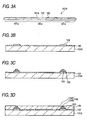
- a semiconductor substrate 101A (a wafer which will be hereinafter referred to as a substrate 101A) having a plurality of regions 101a (like a grid, for example) in which an electronic circuit is formed is manufactured by using a well-known method at a step shown in Fig. 3A .
- the region 101a corresponds to one semiconductor chip 101.
- An electrode pad 103 is formed on a device forming surface 101b of the region 101a on which an electronic circuit is formed.
- a protecting layer (a passivation layer) 102 formed of SiN (Si 3 N 4 ) is provided in a portion other than the electrode pad 103 in the device forming surface 101b. Consequently, the device forming surface 101b is protected.
- Fig. 3B shows the enlarged region 101a of the substrate 101A illustrated in Fig. 3A .
- the region 101a is enlarged for convenience of illustration and explanation.
- a bump 104 is formed on the electrode pad 103 by using a wire bonding device, for example.
- the bump 104 is formed through a bonding wire formed of Au.
- the wire bonding device continuously bonds the bonding wire to the electrode pad 103 and cuts the bonding wire after the bonding, thereby forming a bump body 104 to be bonded to the electrode pad 103 and a protruded portion 104B which is protruded from the bump body 104A.
- an insulating layer 105 formed by an epoxy based resin material is laminated (stuck) onto the substrate 101A (the protecting layer 102).
- the insulating layer 105 it is preferable to use a soft resin material to which a hardness regulating material such as a filler referred to as NCF is rarely added, for example.
- the bump 104 is positioned in the insulating layer 105.
- a tip of the protruded portion 104B does not need to be exposed from an upper surface of the insulating layer 105.
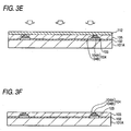
- a copper foil 112 is provided on the insulating layer 105 and a pressure bonding treatment is carried out as shown in Fig. 3E . Consequently, the insulating layer 105 is also pressed so that a part of the protruded portion 104B in the bump 104 is exposed from an upper surface of the insulating layer 105.
- the NCF to be the insulating layer 105 is a soft resin material. Therefore, it is possible to reliably expose the protruded portion 104B from the insulating layer 105. Moreover, a thickness of the insulating layer 105 is also selected in such a manner that the protruded portion 104B is reliably protruded from the upper surface of the insulating layer 105 in the pressure bonding treatment. By the pressure bonding treatment, furthermore, the protruded portion 104B of the bump 104 is pressed by the copper foil 112 and a height of a tip portion thereof is made uniform (leveling).
- the copper foil 112 to be used in this case has a rough surface at an opposed side to the insulating layer 105. For this reason, the rough surface of the copper foil 112 is maintained to be transferred to a surface of the insulating layer 105 to which the copper foil 112 is pressure bonded (which will be described below).
- a material of the insulating layer 105 is not restricted to the NCF but various insulating materials (resin materials) can be used.
- various insulating materials resin materials
- a layer to be formed on the insulating layer 105 does not always need to be the copper foil 112 but a temporary film formed of PET can also be used.
- Fig. 3F shows a state in which the copper foil 112 is removed.
- the protruded portion 104B is exposed from the insulating layer 105 and is subjected to leveling in the pressure bonding treatment. In the state in which the copper foil 112 is removed, therefore, the protruded portion 104B is exposed from the insulating layer 105.
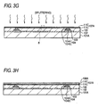
- a first conductive layer 107A is formed on the upper surfaces of the insulating layer 105 and the bump body 104A.
- the example is characterized in that the first conductive layer 107A (the first conductive pattern 107) is formed by using a sputtering process to be a kind of depositing process.
- the first conductive layer 107A has a structure in which a Ti film 114 and a Cu film 115 are laminated. Therefore, sputtering is first carried out by using Ti as a target to form the Ti film 114, and subsequently, the sputtering is carried out by using Cu as a target to form the Cu film 115 in order to form the first conductive layer 107A on the insulating layer 105.
- the Ti film 114 and the Cu film 115 can be continuously formed by using an identical sputtering device.
- a thickness of the Ti film 114 is set to be 0.1 ⁇ m and a thickness of the Cu film 115 is set to be 1.0 ⁇ m (in Figs. 3G and 3H , the Ti film 114 and the Cu film 115 are exaggeratedly drawn to be thicker than the other layers for convenience of illustration).
- the thickness and the material are not restricted.
- the conductive layer 107A (the Ti film 114, the Cu film 115) is formed by using the sputtering process as described above. For this reason, the protruded portion 104B exposed from the insulating layer 105 and the Ti film 114 are metallically bonded to each other (in the case in which the conductive layer 107A is set to have the single layer structure of the Cu film, the protruded portion 104B and the Cu film are metallically bonded to each other).
- the Cu film 115 is also formed on the Ti film 114 by using the sputtering process. Therefore, the Ti film 114 and the Cu film 115 are also bonded metallically.
- the conductive layer 107A (the Ti film 114) is provided on the upper surface of the insulating layer 105 to be the resin through the sputtering. For this reason, there is an apprehension of the bonding property of the insulating layer 105 and the first conductive pattern 107.
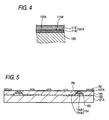
- the copper foil 112 having the single side roughened is used as described above. Consequently, the rough surface of the copper foil 112 is transferred to the surface of the insulating layer 105 in a state in which the copper foil 112 is removed (see Fig. 3F ). In other words, as shown in an enlarged view of Fig. 4 , a rough surface 105A is formed on the surface of the insulating layer 105 in the state in which the copper foil 112 is removed.
- the Ti film 114 is provided on the insulating layer 105 having the rough surface 105A formed thereon through the sputtering process. Consequently, the Ti film 114 is brought into such a state as to cut into concavo-convex portions of the rough surface 105A so that a so-called anchor effect is generated between the insulating layer 105 and the Ti film 114. Even if the insulating layer 105 is a resin, consequently, the Ti film 114 can be reliably formed on the insulating layer 105. Therefore, it is possible to prevent peeling of the Ti film 114 from the insulating layer 105, thereby enhancing the reliability of the semiconductor device 100.
- Fig. 4 is a view showing an enlarged region surrounded by a broken line indicated as B in Fig. 3G .
- a conductive pattern 106 to be connected to the bump 104 is formed through electrolytic plating using the conductive layer 107A as a feeding layer (a seed layer).
- a method of forming the conductive pattern 106 includes so-called subtractive and semiadditive processes, for instance. In the example, description will be given to an example in which the subtractive process is used.
- a conductive layer 108A formed of Cu is laminated on the conductive layer 107A through the electrolytic plating using the conductive layer 107A (the Ti film 114, the Cu film 115) as the feeding layer.
- a mask pattern R1 having an opening portion Ra is formed on the conductive layer 108A.
- the mask pattern R1 can be formed by forming a resist layer through an application or sticking of a film and patterning the resist layer using a photolithographic process.
- the conductive layers 107A and 108A are subjected to pattern etching using the mask pattern R1 as a mask. Consequently, a first conductive layer 107 and a second conductive layer 108 are laminated, and a conductive pattern 106 connected to the bump 104 is formed.
- the first conductive pattern 107 is formed to have a thickness of approximately 1 to 2 ⁇ m and the second conductive pattern 108 is formed to have a thickness of approximately 10 to 30 ⁇ m, and the numeric values are only illustrative and the invention is not restricted to the numeric values.
- the electrolytic plating process In order to form the conductive pattern 106, it is easy to use the electrolytic plating process by setting the conductive layer 107A to be the feeding layer. In the case in which the feeding layer (seed layer) is formed through a nonelectrolytic plating process, for example, it is necessary to carry out a treatment for roughening a surface of an insulating layer (a so-called desmear treatment). Thus, a treatment for forming a plated layer is complicated.
- the desmear treatment is not required. Consequently, it is possible to easily form the feeding layer (the conductive layer 107A) by a simple method. According to the method, therefore, a method of manufacturing a semiconductor device is simplified so that a manufacturing cost is reduced.
- a roughening treatment is carried out over a surface of the conductive pattern 106 (Cu) if necessary, and a solder resist layer (an insulating layer) 109 having an opening portion 109A is then formed on the insulating layer 105. A part of the conductive pattern 106 is exposed from the opening portion 109A.
- a solder bump 110 is formed on the conductive pattern 106 exposed from the opening portion 109A if necessary. Furthermore, the substrate 101A is subjected to dicing to divide the semiconductor chip into pieces. Consequently, it is possible to manufacture the semiconductor device 100 shown in Fig. 1 .
- the conductive pattern 106 is formed by the subtractive process in the manufacturing method, it may be formed by using the semiadditive process. In this case, for example, it is preferable to execute the steps shown in Figs. 3A to 3G in the manufacturing method and to then carry out steps which will be described below in place of the steps shown in Figs. 3H to 3J .
- a mask pattern R2 having an opening portion Rb is formed on a conductive layer 107A.
- the mask pattern R2 can be formed by forming a resist layer through an application or sticking of a film and patterning the resist layer using a photolithographic process.
- electrolytic plating using the conductive layer 107A as a feeding layer (a seed layer) is executed to form a second conductive pattern on the conductive layer 107A exposed from the opening portion Rb.
- the mask pattern R2 is peeled, and furthermore, the excessive feeding layer 107A exposed by peeling the mask pattern R2 is removed by etching. Consequently, it is possible to form the conductive pattern 106 shown in Fig. 3J .
- the substrate 101A it is also possible to use a glass substrate or a multilayer wiring board for the substrate 101A in place of the semiconductor substrate. Accordingly, it is possible to carry out an application to various electronic devices using the substrates.
- the depositing process is not restricted to the sputtering process but a vacuum deposition process or a physical vapor deposition process such as ion plating can also be used, and furthermore, a chemical vapor deposition process such as a CVD process can be used.
Landscapes
- Internal Circuitry In Semiconductor Integrated Circuit Devices (AREA)
- Wire Bonding (AREA)
- Manufacturing Of Printed Wiring (AREA)
Abstract
Description
- The present invention relates to a method of manufacturing an electronic device and to an electronic device, and more particularly, to a method of manufacturing an electronic device having a structure in which a substrate body and a conductive pattern formed thereon through an insulating layer are connected to each other by using a bump, and to a corresponding electronic device.
- For example, there has variously been provided an electronic apparatus in which an electrode and a conductive pattern are formed on a substrate body such as a semiconductor substrate. As one of types, a semiconductor device referred to as a chip size package has been provided.
- The chip size package has a structure in which a rewiring (a conductive layer) is formed through an insulating layer (a protecting layer) on a surface of a semiconductor chip obtained by dicing a wafer to be a semiconductor substrate on which a device is formed.
- In order to manufacture the chip size package, a plurality of electrodes is first formed on a semiconductor chip region of a semiconductor wafer and a bump is formed on each of the electrodes. The bump is formed through a bonding wire by using a bonding device.
- Moreover, an insulating layer is formed on the semiconductor wafer having the bump formed thereon in order to protect a circuit surface formed on the wafer. In this case, a tip portion of the bump is formed to be exposed from the insulating layer.
- Subsequently, a rewiring is formed on an upper part of the insulating layer by using a plating process or a printing process, for example. For a method of electrically bonding the rewiring to the bump, there has been employed a method of connecting the bump to the rewiring through pressure bonding or a method of connecting them by using a conductive paste as is disclosed in Patent Document 1 (=
JP-A-2005-353913 - Then, the wafer is divided into pieces through dicing so that a chip size package is formed.
- In the method of bonding the bump to the rewiring through pressure bonding or a conductive paste, however, the electrical connection of the bump and the rewiring is not sufficient so that a connecting resistance is increased. In the case in which a semiconductor chip has a high speed, therefore, there is a possibility that an electrical characteristic might be deteriorated due to a high connecting impedance. In the method of bonding the bump to the rewiring through pressure bonding or a conductive paste, moreover, there is a problem in that a mechanical connecting property of the bump and the rewiring is not sufficient and a sufficient reliability might not be thus obtained.
- In consideration of the respects, it is an object of the invention to provide a method of manufacturing an electronic device and the electronic device which can enhance electrical and mechanical reliability, and / or which can reduce some other of the above problems. The object is solved by the method of manufacturing an electronic device according to independent claim 1, and by the electronic device according to independent claim 8. Further advantages, features, aspects and details of the invention are evident from the dependent claims, the description and the drawings.
- According to a first aspect of the invention, there is provided a method of manufacturing an electronic device including:
- a first step of forming a bump having a protruded portion on an electrode pad formed on a substrate body;
- a second step of forming an insulating layer on the substrate body and exposing a part of the protruded portion to an upper surface of the insulating layer;
- a third step of forming a conductive layer by using a depositing process in the upper surface of the insulating layer and an exposed part of the protruded portion;
- a fourth step of forming a wiring layer through electrolytic plating using the conductive layer as a feeding layer; and
- a fifth step of patterning the wiring layer to form a conductive pattern connected to the bump.
- According to a second aspect of the invention, there is provided the method of manufacturing an electronic device according to the first aspect, wherein
the substrate body is a semiconductor substrate. - According to a third aspect of the invention, there is provided the method of manufacturing an electronic device according to the first or second aspect, wherein
the depositing process to be executed at the third step is a physical vapor deposition process. - According to a forth aspect of the invention, there is provided the method of manufacturing an electronic device according to any one of the first to third aspects, wherein
at the third step, a bonding metal film such as titanium is first formed as the conductive layer, and a copper film is then formed on the bonding metal film. - According to a fifth aspect of the invention, there is provided the method of manufacturing an electronic device according to any one of the first to third aspects, wherein
at the third step, a copper film is formed as the conductive layer. - According to a sixth aspect of the invention, there is provided the method of manufacturing an electronic device according to any one of the first to fifth aspects, wherein
at the first step, the bump is formed through a bonding wire. - Furthermore, according to a seventh aspect of the invention, there is provided an electronic device including:
- a substrate body having an electrode pad formed thereon;
- a bump formed on the electrode pad;
- an insulating layer formed on the substrate body; and
- a conductive pattern formed on the insulating layer and connected to the bump, wherein
- the bump and the conductive pattern are metallically bonded to each other.
- According to an eighth aspect of the invention, there is provided the electronic device according to the seventh aspect, wherein
the substrate body is a semiconductor chip.
According to a further aspect of the invention, there is provided a method of manufacturing an electronic device having the steps of forming a bump having a protruded portion on an electrode pad formed on a substrate, forming an insulating layer on the substrate and exposing a part of the protruded portion to an upper surface of the insulating layer, forming a first conductive pattern by using a depositing process in the upper surface of the insulating layer and an exposed part of the protruded portion, carrying out electrolytic plating by using the first conductive pattern as a feeding layer, thereby forming a second conductive pattern, and patterning the second conductive pattern to form a conductive pattern connected to the bump. - According to aspects of the invention, the conductive layer is formed by using the depositing process. Therefore, it is possible to metallically bond the bump (the protruded portion) to the conductive layer. Therefore, it is possible to bring the electrical and mechanical connection of the bump and the conductive layer into an excellent state and to enhance an electrical and mechanical reliability in a bonding position of the bump and the conductive layer.
The invention is also directed to apparatuses for carrying out the disclosed methods and including apparatus parts for performing each described method steps. These method steps may be performed by way of hardware components, a computer programmed by appropriate software, by any combination of the two or in any other manner. Furthermore, the invention is also directed to methods by which the described apparatus operates. It includes method steps for carrying out every function of the apparatus or manufacturing every part of the apparatus. - The invention will be better understood by reference to the following description of embodiments of the invention taken in conjunction with the accompanying drawings, wherein:
-
Fig. 1 is a sectional view showing a semiconductor device according to an example of the invention, -
Fig. 2 is a sectional view showing the enlarged vicinity of a bump inFig. 1 , -
Fig. 3A is a sectional view (No. 1) for explaining a method of manufacturing a semiconductor device according to the example of the invention, -
Fig. 3B is a sectional view (No. 2) for explaining the method of manufacturing a semiconductor device according to the example of the invention, -
Fig. 3C is a sectional view (No. 3) for explaining the method of manufacturing a semiconductor device according to the example of the invention, -
Fig. 3D is a sectional view (No. 4) for explaining the method of manufacturing a semiconductor device according to the example of the invention, -
Fig. 3E is a sectional view (No. 5) for explaining the method of manufacturing a semiconductor device according to the example of the invention, -
Fig. 3F is a sectional view (No. 6) for explaining the method of manufacturing a semiconductor device according to the example of the invention, -
Fig. 3G is a sectional view (No. 7) for explaining the method of manufacturing a semiconductor device according to the example of the invention, -
Fig. 3H is a sectional view (No. 8) for explaining the method of manufacturing a semiconductor device according to the example of the invention, -
Fig. 3I is a sectional view (No. 9) for explaining the method of manufacturing a semiconductor device according to the example of the invention, -
Fig. 3J is a sectional view (No. 10) for explaining the method of manufacturing a semiconductor device according to the example of the invention, -
Fig. 3K is a sectional view (No. 11) for explaining the method of manufacturing a semiconductor device according to the example of the invention, -
Fig. 3L is a sectional view (No. 12) for explaining the method of manufacturing a semiconductor device according to the example of the invention, -
Fig. 3M is a sectional view (No. 13) for explaining the method of manufacturing a semiconductor device according to the example of the invention, -
Fig. 4 is a sectional view showing the enlarged vicinity of a Ti film and a Cu film inFig. 3G , and -
Fig. 5 is a sectional view for explaining a variant of the method of manufacturing a semiconductor device according to the example of the invention. - Next, the best mode for carrying out the invention will be described with reference to the drawings.
-
Fig. 1 shows an electronic device according to an example of the invention. In the example, description will be given by taking, as an example of the electronic device, a semiconductor device 100 (CSP) set to have a chip size. - The
semiconductor device 100 according to the example has a structure in which an insulatinglayer 105 and aconductive pattern 106 are laminated and formed on a protecting layer (a passivation layer) 102 of asemiconductor chip 101 on which anelectrode pad 103 is formed. Moreover, abump 104 constituted by Au is formed on theelectrode pad 103, for example. Thebump 104 is formed through a bonding wire by using a wire bonding device, for example. - The
conductive pattern 106 is referred to as a so-called rewiring in some cases and is provided to cause a position of theelectrode pad 103 of thesemiconductor chip 101 to be different from that of asolder bump 110 serving as an external connecting terminal (in order to carry out fan in and a terminal arrangement in an optional position). Moreover, the insulatinglayer 105 is constituted by an epoxy based resin, for example, and serves to protect a surface (a main surface) of thesemiconductor chip 101 on which a circuit is formed and serves as a base material in the formation of theconductive pattern 106. - The
conductive pattern 106 has a structure in which a firstconductive pattern 107 and a secondconductive pattern 108 are laminated, and furthermore, the firstconductive pattern 107 has a structure in which aTi film 114 and aCu film 115 are laminated as shown in an enlarged view ofFig. 2 . - The example is characterized in that the first conductive pattern 107 (the
Ti film 114, the Cu film 115) is formed by a sputtering process (a PVD process) to be a kind of depositing process. Consequently, the first conductive pattern 107 (the Ti film 114) is metallically bonded to the bump 104 (aprotruded portion 104B). Thus, it is possible to enhance an electrical and mechanical connecting property of the firstconductive pattern 107 and thebump 104.Fig. 2 is a view showing an enlarged region (the vicinity of the bump 104) of thesemiconductor device 100 which is surrounded by a broken line indicated as A inFig. 1 . - As described above, the first
conductive pattern 107 is connected to thebump 104 so that theconductive pattern 106 is connected to an electronic circuit of thesemiconductor chip 101 through thebump 104. A solder resist layer (an insulating layer) 109 is formed to cover the insulatinglayer 105 and a part of theconductive pattern 106 around thesolder bump 110. - On the other hand, the
bump 104 is constituted by abump body 104A to be bonded to theelectrode pad 103 and the protrudedportion 104B which is protruded from thebump body 104A as shown inFig. 2 . Thebump 104 is formed by a bonding wire constituted by Au, for example, through a wire bonding device. - The wire bonding device continuously bonds the bonding wire to the
electrode pad 103 and cuts the bonding wire after the bonding, thereby forming thebump body 104A to be bonded to thebump 103 and the protrudedportion 104B which is protruded from thebump body 104A. - The
semiconductor device 100 according to the example has a structure in which the bump 104 (more specifically, the upper surface of the protrudedportion 104B) and the conductive pattern 106 (more specifically, the Ti film 114) are metallically bonded to each other as described above. In order to implement the metallic bonding, theTi film 114 and the protrudedportion 104B are bonded to each other by using a sputtering process in the example. - As in the example, the
bump 104 and theconductive pattern 106 are metallically bonded to each other. Consequently, it is possible to enhance both electrical and mechanical bonding properties of thebump 104 and theconductive pattern 106. Thus, it is possible to enhance a reliability of thesemiconductor device 100. - Next, a method of manufacturing the
semiconductor device 100 will be described with reference toFigs. 3A to 3M . InFigs. 3A to 3M , corresponding structures to those shown inFigs. 1 and 2 have the same reference numerals and description thereof will be omitted. - In order to manufacture the
semiconductor device 100, first of all, asemiconductor substrate 101A (a wafer which will be hereinafter referred to as asubstrate 101A) having a plurality ofregions 101a (like a grid, for example) in which an electronic circuit is formed is manufactured by using a well-known method at a step shown inFig. 3A . - The
region 101a corresponds to onesemiconductor chip 101. Anelectrode pad 103 is formed on adevice forming surface 101b of theregion 101a on which an electronic circuit is formed. Moreover, a protecting layer (a passivation layer) 102 formed of SiN (Si3N4) is provided in a portion other than theelectrode pad 103 in thedevice forming surface 101b. Consequently, thedevice forming surface 101b is protected. -
Fig. 3B shows theenlarged region 101a of thesubstrate 101A illustrated inFig. 3A . InFig. 3B and succeeding drawings, theregion 101a is enlarged for convenience of illustration and explanation. - At a step shown in
Fig. 3C , abump 104 is formed on theelectrode pad 103 by using a wire bonding device, for example. Thebump 104 is formed through a bonding wire formed of Au. The wire bonding device continuously bonds the bonding wire to theelectrode pad 103 and cuts the bonding wire after the bonding, thereby forming abump body 104 to be bonded to theelectrode pad 103 and a protrudedportion 104B which is protruded from thebump body 104A. - At a step shown in
Fig. 3D , next, an insulatinglayer 105 formed by an epoxy based resin material, for example, is laminated (stuck) onto thesubstrate 101A (the protecting layer 102). For the insulatinglayer 105, it is preferable to use a soft resin material to which a hardness regulating material such as a filler referred to as NCF is rarely added, for example. In a state in which the insulatinglayer 105 is disposed, thebump 104 is positioned in the insulatinglayer 105. However, a tip of the protrudedportion 104B does not need to be exposed from an upper surface of the insulatinglayer 105. - Next, a
copper foil 112 is provided on the insulatinglayer 105 and a pressure bonding treatment is carried out as shown inFig. 3E . Consequently, the insulatinglayer 105 is also pressed so that a part of the protrudedportion 104B in thebump 104 is exposed from an upper surface of the insulatinglayer 105. - In this case, the NCF to be the insulating
layer 105 is a soft resin material. Therefore, it is possible to reliably expose the protrudedportion 104B from the insulatinglayer 105. Moreover, a thickness of the insulatinglayer 105 is also selected in such a manner that the protrudedportion 104B is reliably protruded from the upper surface of the insulatinglayer 105 in the pressure bonding treatment. By the pressure bonding treatment, furthermore, the protrudedportion 104B of thebump 104 is pressed by thecopper foil 112 and a height of a tip portion thereof is made uniform (leveling). - The
copper foil 112 to be used in this case has a rough surface at an opposed side to the insulatinglayer 105. For this reason, the rough surface of thecopper foil 112 is maintained to be transferred to a surface of the insulatinglayer 105 to which thecopper foil 112 is pressure bonded (which will be described below). - A material of the insulating
layer 105 is not restricted to the NCF but various insulating materials (resin materials) can be used. For example, it is also possible to use, as the insulatinglayer 105, a buildup resin (an epoxy resin containing a filler) or a resin material referred to as ACF. Moreover, a layer to be formed on the insulatinglayer 105 does not always need to be thecopper foil 112 but a temporary film formed of PET can also be used. Furthermore, it is also possible to use a resin film having a single surface coated with a copper foil in which a Cu foil is previously provided on a single side of a resin film. - When the pressure bonding treatment is ended, for example, the
copper foil 112 is removed by using an etching process, for example.Fig. 3F shows a state in which thecopper foil 112 is removed. As described above, the protrudedportion 104B is exposed from the insulatinglayer 105 and is subjected to leveling in the pressure bonding treatment. In the state in which thecopper foil 112 is removed, therefore, the protrudedportion 104B is exposed from the insulatinglayer 105. - At a step shown in
Fig. 3G , next, a firstconductive layer 107A is formed on the upper surfaces of the insulatinglayer 105 and thebump body 104A. The example is characterized in that the firstconductive layer 107A (the first conductive pattern 107) is formed by using a sputtering process to be a kind of depositing process. - The first
conductive layer 107A has a structure in which aTi film 114 and aCu film 115 are laminated. Therefore, sputtering is first carried out by using Ti as a target to form theTi film 114, and subsequently, the sputtering is carried out by using Cu as a target to form theCu film 115 in order to form the firstconductive layer 107A on the insulatinglayer 105. TheTi film 114 and theCu film 115 can be continuously formed by using an identical sputtering device. - In the example, moreover, a thickness of the
Ti film 114 is set to be 0.1µm and a thickness of theCu film 115 is set to be 1.0µm (inFigs. 3G and 3H , theTi film 114 and theCu film 115 are exaggeratedly drawn to be thicker than the other layers for convenience of illustration). Referring to theTi film 114, however, the thickness and the material are not restricted. For example, it is also possible to use a Cr film having a thickness of 0.035µm in place of theTi film 114. Furthermore, it is also possible to carry out the sputtering by using Cu as a target, thereby causing the firstconductive pattern 107 to have a single layer structure of the Cu film without setting the firstconductive pattern 107 to have the lamination structure of theTi film 114 and theCu film 115. - In the example, the
conductive layer 107A (theTi film 114, the Cu film 115) is formed by using the sputtering process as described above. For this reason, the protrudedportion 104B exposed from the insulatinglayer 105 and theTi film 114 are metallically bonded to each other (in the case in which theconductive layer 107A is set to have the single layer structure of the Cu film, the protrudedportion 104B and the Cu film are metallically bonded to each other). Moreover, theCu film 115 is also formed on theTi film 114 by using the sputtering process. Therefore, theTi film 114 and theCu film 115 are also bonded metallically. - As compared with the bonding method using pressure bonding or a conductive paste according to the conventional art, accordingly, it is possible to bond the
bump 104 to theconductive layer 107A more strongly and to enhance their mechanical and electrical connecting properties more greatly. - In the example, the
conductive layer 107A (the Ti film 114) is provided on the upper surface of the insulatinglayer 105 to be the resin through the sputtering. For this reason, there is an apprehension of the bonding property of the insulatinglayer 105 and the firstconductive pattern 107. In the example, however, thecopper foil 112 having the single side roughened is used as described above. Consequently, the rough surface of thecopper foil 112 is transferred to the surface of the insulatinglayer 105 in a state in which thecopper foil 112 is removed (seeFig. 3F ). In other words, as shown in an enlarged view ofFig. 4 , arough surface 105A is formed on the surface of the insulatinglayer 105 in the state in which thecopper foil 112 is removed. - Accordingly, the
Ti film 114 is provided on the insulatinglayer 105 having therough surface 105A formed thereon through the sputtering process. Consequently, theTi film 114 is brought into such a state as to cut into concavo-convex portions of therough surface 105A so that a so-called anchor effect is generated between the insulatinglayer 105 and theTi film 114. Even if the insulatinglayer 105 is a resin, consequently, theTi film 114 can be reliably formed on the insulatinglayer 105. Therefore, it is possible to prevent peeling of theTi film 114 from the insulatinglayer 105, thereby enhancing the reliability of thesemiconductor device 100. - As shown in
Fig. 4 , moreover, therough surface 105A of the insulatinglayer 105 is also transferred to asurface 114A of theTi film 114 formed thereon so that thesurface 114A also becomes a rough surface. Therefore, the anchor effect is also generated between thesurface 114A and theCu film 115 formed thereon so that the bonding property of theTi film 114 and theCu film 115 can be enhanced.Fig. 4 is a view showing an enlarged region surrounded by a broken line indicated as B inFig. 3G . - At steps shown in
Figs. 3H to 3J , next, aconductive pattern 106 to be connected to thebump 104 is formed through electrolytic plating using theconductive layer 107A as a feeding layer (a seed layer). A method of forming theconductive pattern 106 includes so-called subtractive and semiadditive processes, for instance. In the example, description will be given to an example in which the subtractive process is used. - At the step shown in
Fig. 3H , first of all, aconductive layer 108A formed of Cu, for example, is laminated on theconductive layer 107A through the electrolytic plating using theconductive layer 107A (theTi film 114, the Cu film 115) as the feeding layer. At the step shown inFig. 3I , next, a mask pattern R1 having an opening portion Ra is formed on theconductive layer 108A. The mask pattern R1 can be formed by forming a resist layer through an application or sticking of a film and patterning the resist layer using a photolithographic process. - At the step shown in
Fig. 3J , then, theconductive layers conductive layer 107 and a secondconductive layer 108 are laminated, and aconductive pattern 106 connected to thebump 104 is formed. - For example, the first
conductive pattern 107 is formed to have a thickness of approximately 1 to 2µm and the secondconductive pattern 108 is formed to have a thickness of approximately 10 to 30 µm, and the numeric values are only illustrative and the invention is not restricted to the numeric values. - In order to form the
conductive pattern 106, it is easy to use the electrolytic plating process by setting theconductive layer 107A to be the feeding layer. In the case in which the feeding layer (seed layer) is formed through a nonelectrolytic plating process, for example, it is necessary to carry out a treatment for roughening a surface of an insulating layer (a so-called desmear treatment). Thus, a treatment for forming a plated layer is complicated. - On the other hand, in the method according to the example, the desmear treatment is not required. Consequently, it is possible to easily form the feeding layer (the
conductive layer 107A) by a simple method. According to the method, therefore, a method of manufacturing a semiconductor device is simplified so that a manufacturing cost is reduced. - At a step shown in
Fig. 3K , thereafter, a roughening treatment is carried out over a surface of the conductive pattern 106 (Cu) if necessary, and a solder resist layer (an insulating layer) 109 having an openingportion 109A is then formed on the insulatinglayer 105. A part of theconductive pattern 106 is exposed from theopening portion 109A. - At a step shown in
Fig. 3L , subsequently, back grinding is carried out over thesubstrate 101A if necessary, thereby causing thesubstrate 101A to have a certain thickness. - At a step shown in
Fig. 3M , subsequently, asolder bump 110 is formed on theconductive pattern 106 exposed from theopening portion 109A if necessary. Furthermore, thesubstrate 101A is subjected to dicing to divide the semiconductor chip into pieces. Consequently, it is possible to manufacture thesemiconductor device 100 shown inFig. 1 . - While the
conductive pattern 106 is formed by the subtractive process in the manufacturing method, it may be formed by using the semiadditive process. In this case, for example, it is preferable to execute the steps shown inFigs. 3A to 3G in the manufacturing method and to then carry out steps which will be described below in place of the steps shown inFigs. 3H to 3J . - More specifically, as shown in
Fig. 5 , a mask pattern R2 having an opening portion Rb is formed on aconductive layer 107A. The mask pattern R2 can be formed by forming a resist layer through an application or sticking of a film and patterning the resist layer using a photolithographic process. - Next, electrolytic plating using the
conductive layer 107A as a feeding layer (a seed layer) is executed to form a second conductive pattern on theconductive layer 107A exposed from the opening portion Rb. Then, the mask pattern R2 is peeled, and furthermore, theexcessive feeding layer 107A exposed by peeling the mask pattern R2 is removed by etching. Consequently, it is possible to form theconductive pattern 106 shown inFig. 3J . - While the invention is described above based on the preferred examples, the invention is not restricted to the specific examples but various modifications and changes can be made without departing from the gist described in the claims.
- More specifically, it is also possible to use a glass substrate or a multilayer wiring board for the
substrate 101A in place of the semiconductor substrate. Accordingly, it is possible to carry out an application to various electronic devices using the substrates. - Moreover, the depositing process is not restricted to the sputtering process but a vacuum deposition process or a physical vapor deposition process such as ion plating can also be used, and furthermore, a chemical vapor deposition process such as a CVD process can be used.
Claims (10)
- A method of manufacturing an electronic device comprising:a first step of forming a bump (104) having a protruded portion (104B) on an electrode pad (103) formed on a substrate body (101A);a second step of forming an insulating layer (105) on the substrate body (101A) and exposing a part of the protruded portion (104B) to an upper surface of the insulating layer (105);a third step of forming a conductive layer (107) by using a depositing process in the upper surface of the insulating layer (105) and an exposed part of the protruded portion (104B);a fourth step of forming a wiring layer (108) through electrolytic plating using the conductive layer (107) as a feeding layer; anda fifth step of patterning the wiring layer (108) to form a conductive pattern (106) connected to the bump (104).
- The method of manufacturing an electronic device according to claim 1, wherein
the substrate body is a semiconductor substrate. - The method of manufacturing an electronic device according to any one of the preceding claims, wherein
the depositing process to be executed at the third step is a physical vapor deposition process. - The method of manufacturing an electronic device according to any one of the preceding claims, wherein
at the third step, a bonding metal film is first formed as the conductive layer, and a copper film is then formed on the bonding metal film. - The method of manufacturing an electronic device according to any one of the preceding claims, wherein
at the third step, a copper film is formed as the conductive layer. - The method of manufacturing an electronic device according to any one of the preceding claims, wherein
at the first step, the bump is formed through a bonding wire. - The method of manufacturing an electronic device according to any one of claims 4 to 6, wherein
the bonding metal film is a Ti film. - An electronic device comprising:a substrate body (101A) having an electrode pad (103) formed thereon;a bump (104) formed on the electrode pad;an insulating layer (105) formed on the substrate body; anda conductive pattern (106) formed on the insulating layer (105) and connected to the bump (104), whereinthe bump (104) and the conductive pattern (106) are metallically bonded to each other.
- The electronic device according to claim 8, wherein
the substrate body is a semiconductor chip. - The electronic device according to claim 8 or 9, wherein the bump has a protruded portion.
Applications Claiming Priority (1)
| Application Number | Priority Date | Filing Date | Title |
|---|---|---|---|
| JP2007160613A JP4121542B1 (en) | 2007-06-18 | 2007-06-18 | Manufacturing method of electronic device |
Publications (2)
| Publication Number | Publication Date |
|---|---|
| EP2048712A2 true EP2048712A2 (en) | 2009-04-15 |
| EP2048712A3 EP2048712A3 (en) | 2009-11-04 |
Family
ID=39704898
Family Applications (1)
| Application Number | Title | Priority Date | Filing Date |
|---|---|---|---|
| EP08158510A Withdrawn EP2048712A3 (en) | 2007-06-18 | 2008-06-18 | Electronic device manufacturing method and electronic device |
Country Status (6)
| Country | Link |
|---|---|
| US (1) | US7795127B2 (en) |
| EP (1) | EP2048712A3 (en) |
| JP (1) | JP4121542B1 (en) |
| KR (1) | KR20080111397A (en) |
| CN (1) | CN101330028A (en) |
| TW (1) | TW200901347A (en) |
Families Citing this family (10)
| Publication number | Priority date | Publication date | Assignee | Title |
|---|---|---|---|---|
| JP5436836B2 (en) | 2008-10-30 | 2014-03-05 | 新光電気工業株式会社 | Manufacturing method of semiconductor device embedded substrate |
| JP5436837B2 (en) | 2008-10-30 | 2014-03-05 | 新光電気工業株式会社 | Manufacturing method of semiconductor device embedded substrate |
| JP5406572B2 (en) * | 2009-03-19 | 2014-02-05 | 新光電気工業株式会社 | Electronic component built-in wiring board and manufacturing method thereof |
| JP5466096B2 (en) * | 2010-06-21 | 2014-04-09 | 新光電気工業株式会社 | Semiconductor device and manufacturing method thereof |
| JP5590984B2 (en) * | 2010-06-21 | 2014-09-17 | 新光電気工業株式会社 | Electronic device and manufacturing method thereof |
| JP5590985B2 (en) | 2010-06-21 | 2014-09-17 | 新光電気工業株式会社 | Semiconductor device and manufacturing method thereof |
| KR101138592B1 (en) * | 2010-08-18 | 2012-05-10 | 삼성전기주식회사 | Board with Fine Pitch Bump and Method of Manufacturing the same |
| JP2012134270A (en) * | 2010-12-21 | 2012-07-12 | Shinko Electric Ind Co Ltd | Semiconductor device and manufacturing method of the same |
| US9041215B2 (en) | 2013-03-12 | 2015-05-26 | Taiwan Semiconductor Manufacturing Company, Ltd. | Single mask package apparatus and method |
| CN113517198A (en) | 2020-04-10 | 2021-10-19 | 长鑫存储技术有限公司 | Semiconductor device and method of making the same |
Citations (1)
| Publication number | Priority date | Publication date | Assignee | Title |
|---|---|---|---|---|
| JP2005353913A (en) | 2004-06-11 | 2005-12-22 | Denso Corp | Semiconductor device and method for manufacturing the same, circuit board |
Family Cites Families (16)
| Publication number | Priority date | Publication date | Assignee | Title |
|---|---|---|---|---|
| JP3313547B2 (en) * | 1995-08-30 | 2002-08-12 | 沖電気工業株式会社 | Manufacturing method of chip size package |
| JP3629178B2 (en) * | 2000-02-21 | 2005-03-16 | Necエレクトロニクス株式会社 | Flip chip type semiconductor device and manufacturing method thereof |
| DE50114493D1 (en) | 2000-05-17 | 2009-01-02 | Eastman Kodak Co | Method for setting the register in a multi-color printing machine |
| JP2002050716A (en) * | 2000-08-02 | 2002-02-15 | Dainippon Printing Co Ltd | Semiconductor device and manufacturing method thereof |
| JP2002313930A (en) * | 2001-04-11 | 2002-10-25 | Matsushita Electric Ind Co Ltd | Semiconductor device and manufacturing method thereof |
| US6743660B2 (en) * | 2002-01-12 | 2004-06-01 | Taiwan Semiconductor Manufacturing Co., Ltd | Method of making a wafer level chip scale package |
| JP3542350B2 (en) * | 2002-05-31 | 2004-07-14 | 沖電気工業株式会社 | Semiconductor device and manufacturing method thereof |
| JP2004047725A (en) | 2002-07-11 | 2004-02-12 | Sumitomo Bakelite Co Ltd | Semiconductor device and manufacturing method |
| US20040191955A1 (en) * | 2002-11-15 | 2004-09-30 | Rajeev Joshi | Wafer-level chip scale package and method for fabricating and using the same |
| JP2004193297A (en) | 2002-12-11 | 2004-07-08 | Dainippon Printing Co Ltd | Wafer level package and method of manufacturing the same |
| JP2004193497A (en) * | 2002-12-13 | 2004-07-08 | Nec Electronics Corp | Chip size package and manufacturing method thereof |
| JP3929966B2 (en) * | 2003-11-25 | 2007-06-13 | 新光電気工業株式会社 | Semiconductor device and manufacturing method thereof |
| JP4105202B2 (en) * | 2006-09-26 | 2008-06-25 | 新光電気工業株式会社 | Manufacturing method of semiconductor device |
| JP4121543B1 (en) * | 2007-06-18 | 2008-07-23 | 新光電気工業株式会社 | Electronic equipment |
| JP4708399B2 (en) * | 2007-06-21 | 2011-06-22 | 新光電気工業株式会社 | Electronic device manufacturing method and electronic device |
| JP5139039B2 (en) * | 2007-11-20 | 2013-02-06 | 新光電気工業株式会社 | Semiconductor device and manufacturing method thereof |
-
2007
- 2007-06-18 JP JP2007160613A patent/JP4121542B1/en not_active Expired - Fee Related
-
2008
- 2008-06-05 TW TW097120902A patent/TW200901347A/en unknown
- 2008-06-16 KR KR1020080056099A patent/KR20080111397A/en not_active Withdrawn
- 2008-06-17 US US12/140,706 patent/US7795127B2/en not_active Expired - Fee Related
- 2008-06-17 CN CNA2008101266191A patent/CN101330028A/en active Pending
- 2008-06-18 EP EP08158510A patent/EP2048712A3/en not_active Withdrawn
Patent Citations (1)
| Publication number | Priority date | Publication date | Assignee | Title |
|---|---|---|---|---|
| JP2005353913A (en) | 2004-06-11 | 2005-12-22 | Denso Corp | Semiconductor device and method for manufacturing the same, circuit board |
Also Published As
| Publication number | Publication date |
|---|---|
| JP4121542B1 (en) | 2008-07-23 |
| JP2008311592A (en) | 2008-12-25 |
| KR20080111397A (en) | 2008-12-23 |
| US7795127B2 (en) | 2010-09-14 |
| CN101330028A (en) | 2008-12-24 |
| EP2048712A3 (en) | 2009-11-04 |
| US20080315414A1 (en) | 2008-12-25 |
| TW200901347A (en) | 2009-01-01 |
Similar Documents
| Publication | Publication Date | Title |
|---|---|---|
| US7795127B2 (en) | Electronic device manufacturing method and electronic device | |
| EP2006908B1 (en) | Electronic device and method of manufacturing the same | |
| JP2004193497A (en) | Chip size package and manufacturing method thereof | |
| EP2017883A2 (en) | Electronic device manufacturing method and electronic device | |
| US7829378B2 (en) | Method of manufacturing electronic device, substrate and semiconductor device | |
| US7981724B2 (en) | Manufacturing method for semiconductor device embedded substrate | |
| CN1311519C (en) | Crystal circular/ chip distribution layer protecting method | |
| EP2075833A2 (en) | Method of manufacturing semiconductor device | |
| US7183190B2 (en) | Semiconductor device and fabrication method therefor | |
| EP1933377B1 (en) | Semiconductor device and method for manufacturing the same | |
| US7915078B2 (en) | Manufacturing method for semiconductor device embedded substrate | |
| JP2007180395A (en) | Manufacturing method of semiconductor device | |
| EP2065928A2 (en) | Semiconductor device and manufacturing method thereof | |
| US7202421B2 (en) | Electronic elements, method for manufacturing electronic elements, circuit substrates, method for manufacturing circuit substrates, electronic devices and method for manufacturing electronic devices | |
| JP2005353837A (en) | Semiconductor device and manufacturing method thereof | |
| US20100112786A1 (en) | Method of manufacturing semiconductor device | |
| US20090168380A1 (en) | Package substrate embedded with semiconductor component | |
| JP5982760B2 (en) | Electronic device and manufacturing method thereof | |
| JP4549693B2 (en) | Wiring board manufacturing method | |
| US7985619B2 (en) | Manufacturing method for semiconductor device embedded substrate | |
| JP2006120803A (en) | Semiconductor device and manufacturing method of semiconductor device | |
| JP2011040610A (en) | Semiconductor device and method of manufacturing the same | |
| CN110709970A (en) | Semiconductor device and method for manufacturing semiconductor device | |
| EP3692572A1 (en) | Structure and method for semiconductor packaging |
Legal Events
| Date | Code | Title | Description |
|---|---|---|---|
| PUAI | Public reference made under article 153(3) epc to a published international application that has entered the european phase |
Free format text: ORIGINAL CODE: 0009012 |
|
| PUAI | Public reference made under article 153(3) epc to a published international application that has entered the european phase |
Free format text: ORIGINAL CODE: 0009012 |
|
| AK | Designated contracting states |
Kind code of ref document: A2 Designated state(s): AT BE BG CH CY CZ DE DK EE ES FI FR GB GR HR HU IE IS IT LI LT LU LV MC MT NL NO PL PT RO SE SI SK TR |
|
| AX | Request for extension of the european patent |
Extension state: AL BA MK RS |
|
| PUAL | Search report despatched |
Free format text: ORIGINAL CODE: 0009013 |
|
| AK | Designated contracting states |
Kind code of ref document: A3 Designated state(s): AT BE BG CH CY CZ DE DK EE ES FI FR GB GR HR HU IE IS IT LI LT LU LV MC MT NL NO PL PT RO SE SI SK TR |
|
| AX | Request for extension of the european patent |
Extension state: AL BA MK RS |
|
| 17P | Request for examination filed |
Effective date: 20100504 |
|
| 17Q | First examination report despatched |
Effective date: 20100531 |
|
| AKX | Designation fees paid |
Designated state(s): DE |
|
| RIC1 | Information provided on ipc code assigned before grant |
Ipc: H01L 21/60 20060101ALI20110314BHEP Ipc: H01L 23/485 20060101ALI20110314BHEP Ipc: H01L 23/31 20060101AFI20110314BHEP |
|
| RTI1 | Title (correction) |
Free format text: ELECTRONIC DEVICE MANUFACTURING METHOD |
|
| STAA | Information on the status of an ep patent application or granted ep patent |
Free format text: STATUS: THE APPLICATION HAS BEEN WITHDRAWN |
|
| 18W | Application withdrawn |
Effective date: 20150312 |