EP2044679B1 - Circuit électrique d'alimentation d'un module de commande comportant deux modes d'alimentation - Google Patents
Circuit électrique d'alimentation d'un module de commande comportant deux modes d'alimentation Download PDFInfo
- Publication number
- EP2044679B1 EP2044679B1 EP07823331.9A EP07823331A EP2044679B1 EP 2044679 B1 EP2044679 B1 EP 2044679B1 EP 07823331 A EP07823331 A EP 07823331A EP 2044679 B1 EP2044679 B1 EP 2044679B1
- Authority
- EP
- European Patent Office
- Prior art keywords
- voltage
- volts
- control module
- signal
- battery
- Prior art date
- Legal status (The legal status is an assumption and is not a legal conclusion. Google has not performed a legal analysis and makes no representation as to the accuracy of the status listed.)
- Not-in-force
Links
Images

Classifications
-
- H—ELECTRICITY
- H02—GENERATION; CONVERSION OR DISTRIBUTION OF ELECTRIC POWER
- H02M—APPARATUS FOR CONVERSION BETWEEN AC AND AC, BETWEEN AC AND DC, OR BETWEEN DC AND DC, AND FOR USE WITH MAINS OR SIMILAR POWER SUPPLY SYSTEMS; CONVERSION OF DC OR AC INPUT POWER INTO SURGE OUTPUT POWER; CONTROL OR REGULATION THEREOF
- H02M3/00—Conversion of DC power input into DC power output
- H02M3/02—Conversion of DC power input into DC power output without intermediate conversion into AC
- H02M3/04—Conversion of DC power input into DC power output without intermediate conversion into AC by static converters
- H02M3/10—Conversion of DC power input into DC power output without intermediate conversion into AC by static converters using discharge tubes with control electrode or semiconductor devices with control electrode
- H02M3/145—Conversion of DC power input into DC power output without intermediate conversion into AC by static converters using discharge tubes with control electrode or semiconductor devices with control electrode using devices of a triode or transistor type requiring continuous application of a control signal
- H02M3/155—Conversion of DC power input into DC power output without intermediate conversion into AC by static converters using discharge tubes with control electrode or semiconductor devices with control electrode using devices of a triode or transistor type requiring continuous application of a control signal using semiconductor devices only
- H02M3/156—Conversion of DC power input into DC power output without intermediate conversion into AC by static converters using discharge tubes with control electrode or semiconductor devices with control electrode using devices of a triode or transistor type requiring continuous application of a control signal using semiconductor devices only with automatic control of output voltage or current, e.g. switching regulators
Definitions
- the present invention relates to an electrical supply circuit of a control module of a heat engine such as those used for the motorization of motor vehicles.
- Such a control module generally called ECU (Engine Control Unit)
- ECU Engine Control Unit
- a digital core such as a microprocessor arranged to manage the fuel injection, the control of the throttle valve ...
- the power supply circuit of the control module generally comprises a battery connected by a main branch to a voltage regulator integrated in the control module to power it.
- the battery is usually that of the motor vehicle, also used to power other engine components such as the starter.
- the battery generally delivers a voltage of 12 volts while the voltage regulator delivers, from this voltage of 12 volts, a voltage of 5 volts and a voltage of 3.3 volts to supply the control module.
- the consumption of the starter causes a drop in the voltage available to the battery and makes it necessary to have in the power supply circuit sufficient capacity to restore the energy to power the control module. It has also been envisaged to raise the voltage supplied by the battery before entering the voltage regulator.
- the document US5,179,508 shows an electrical supply circuit with these technical characteristics.
- an electrical supply circuit of a control module comprising a battery connected by a main branch to a voltage regulator associated with the control module for supplying the module of control, the power supply circuit comprising a secondary branch, in parallel with the main branch, which is connected to a voltage-regulated up-converter and connected to a regulating signal determining member by comparing an image of a signal an output voltage of the step-up converter to a reference signal generated from an output voltage of the voltage regulator, and the main branch being bypassed by the secondary branch when the battery delivers a voltage greater than a predetermined nominal operating threshold.
- the battery supplies the voltage regulator with the secondary branch in which the voltage is high in order to allow the regulator to be powered. voltage.
- the battery directly supplies the voltage regulator via the main branch.
- the secondary branch allows the regulator to be fed during the start-up phases while the main branch supplies the regulator with power outside the start-up phase. .
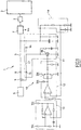
- the electrical supply circuit which is here described and generally designated 1 to the figure 1 , is intended to supply a control module 2 of a motor vehicle engine 3.
- the control module 2 is known in itself.
- the electrical circuit 1 comprises a main branch 5 connecting a battery 6 to a voltage regulator 7 integrated in the control module 2 to power it.
- the battery is here the 12-volt battery of the motor vehicle and is connected to other elements of the motor vehicle and in particular to the starter of the engine 3.
- the voltage regulator 7 is known in itself and here comprises a linear regulator arranged to provide, in particular, a voltage of 5 volts to the control module 2.
- the main branch 5 comprises a diode 8 passing from the battery 6 to the voltage regulator 7.
- the electrical circuit 1 further comprises a secondary branch 9 extending in parallel with the main branch 5 and connected thereto on either side of the diode 8.
- the secondary branch 9 is connected to a voltage-boosting converter , generally designated 10, comprising a power switching circuit 11 operating from pulses produced by a pulse generator circuit 12 operating from a triangular signal, here centered, produced by a triangular signal generator circuit 13 and from a voltage from a voltage divider circuit 14.
- the power switching circuit 11 comprises two diodes 15, 16 arranged in series on the secondary branch 9 and passing the battery 6 to the control module 2, and an inductor 17 disposed between the diodes 15, 16.
- the switching circuit of power 11 comprises in a manner known in itself a transistor 18 N MOSFET whose source and drain are connected to the ground and the secondary branch 9 between the diode 16 and the inductor 17, and the gate is connected to the output of the pulse generator circuit 12.
- the triangular signal generating circuit 13 is produced here in a manner known per se by means of a comparator.
- the triangular signal generating circuit 13 receives as input the voltage coming from the voltage regulator 7 and outputs a triangular signal represented at 100 on the figure 2 .
- the components of the triangular signal generating circuit are selected so that the triangular signal 100 has a minimum voltage of about 2.4 volts and a maximum voltage of about 3.7 volts for an output voltage Vcc of the organ voltage regulator 7 between 4.9 volts and about 5.1 volts.
- the pulse generator circuit 12 (known in itself, PWM type circuit “Pulse Width Modulation”, pulse width modulation) comprises a comparator receiving as positive input the triangular signal 100 and at the negative input the voltage coming from the divider circuit 14 and shown at 200 on the figure 2 .
- the amplifier compares the two signals and outputs, via a transistor arrangement, pulses 300 which feed the gate of transistor 18.
- the divider circuit 14 is powered by the output voltage of the power switching circuit 11 and operates a division of the output voltage of the power switching circuit 11 to supply the voltage 200 to the negative input of the amplifier of the circuit pulse generator 12.
- the output voltage of the divider is thus an image of the output voltage of the step-up converter 10, resulting from a treatment of this voltage.
- the components and mounting of the up-converter 10 are determined to allow the production of a minimum output voltage of about 6 volts for a minimum input voltage of 4.5 volts.
- the divider circuit 14 is arranged in a manner known per se to perform a division such that the output voltage of the divider circuit 14 is 3.7 volts when the output voltage of the power switching circuit 11 is 7.1 volts.
- the components of the main and secondary branches 9 are chosen such that the main branch 5 is in bypass of the secondary branch 9 when the voltage delivered by the battery 6 is greater than a nominal operating threshold of 7.7 volts about.
- the control module 2 is then powered by the main branch 5. Below the nominal operating threshold, the control module 2 is powered by the secondary branch 9. The voltage is then raised analogically to reach a value sufficient to supply the control module 2 via the device regulation 7.
- the reference signal has been described as a centered triangular signal
- the reference signal can have other forms and be especially any signal comprising a succession of patterns, of variable or constant periods, each having a rising portion and a downward portion of which at least one is generally inclined, that is to say a signal comprising a succession of ramps such as a triangular non-centered or sawtooth signal, or with curvilinear portions such as a sinusoidal signal .
- the reference signal may furthermore have a variable amplitude and / or period.
Landscapes
- Engineering & Computer Science (AREA)
- Power Engineering (AREA)
- Charge And Discharge Circuits For Batteries Or The Like (AREA)
- Direct Current Feeding And Distribution (AREA)
- Dc-Dc Converters (AREA)
- Secondary Cells (AREA)
Description
- La présente invention concerne un circuit électrique d'alimentation d'un module de commande d'un moteur thermique comme ceux utilisés pour la motorisation des véhicules automobiles.
- Un tel module de commande, généralement nommé ECU (de l'anglais "Engine Control Unit", unité de commande moteur), comprend un noyau numérique tel qu'un microprocesseur agencé pour gérer l'injection du carburant, le pilotage du papillon des gaz...
- Le circuit électrique d'alimentation du module de commande comporte généralement une batterie reliée par une branche principale à un organe de régulation de tension intégré au module de commande pour alimenter celui-ci. La batterie est généralement celle du véhicule automobile, également utilisée pour alimenter d'autres composants du moteur comme le démarreur. La batterie délivre généralement une tension de 12 volts tandis que l'organe de régulation de tension délivre, à partir de cette tension de 12 volts, une tension de 5 volts et une tension de 3,3 volts pour alimenter le module de commande. Pendant la phase de démarrage, la consommation du démarreur entraîne une chute de la tension disponible à la batterie et rend nécessaire de disposer dans le circuit d'alimentation d'une capacité suffisante pour restituer l'énergie permettant d'alimenter le module de commande. Il a également été envisagé d'élever la tension fournie par la batterie avant son entrée dans l'organe de régulation de tension. Le document
US 5.179.508 montre un circuit électrique d'alimentation avec ces caractéristiques techniques. Il existe des circuits intégrés dédiés pouvant réaliser cette fonction. Ces circuits intégrés sont toutefois coûteux sans être suffisamment robustes pour pouvoir fonctionner dans le compartiment moteur d'un véhicule automobile. On aurait également pu imaginer de programmer le module de commande pour qu'il réalise lui-même cette fonction. Cependant, au moment du démarrage, la charge de calcul du module de commande est importante au point que le module de commande ne pourrait gérer efficacement cette fonction d'élévation de tension. - Il serait donc intéressant de disposer d'un moyen permettant d'alimenter un module de commande de moteur thermique lorsque la tension délivrée par la batterie est relativement faible.
- A cet effet, on prévoit, selon l'invention, un circuit électrique d'alimentation d'un module de commande, comportant une batterie reliée par une branche principale à un organe de régulation de tension associé au module de commande pour alimenter le module de commande, le circuit d'alimentation comprenant une branche secondaire, en parallèle de la branche principale, qui est reliée à un convertisseur élévateur de tension régulé par un signal et relié à un organe de détermination du signal de régulation par comparaison d'une image d'une tension de sortie du convertisseur élévateur de tension à un signal de référence généré à partir d'une tension de sortie de l'organe de régulation de tension, et la branche principale étant montée en by-pass de la branche secondaire lorsque la batterie délivre une tension supérieure à un seuil de fonctionnement nominal prédéterminé.
- Ainsi, lorsque la tension délivrée par la batterie est inférieure au seuil de fonctionnement nominal prédéterminé, la batterie alimente l'organe de régulation de tension par la branche secondaire dans laquelle la tension est élevée pour permettre l'alimentation de l'organe de régulation de tension. Lorsque la tension délivrée par la batterie est supérieure au seuil de fonctionnement nominal prédéterminé, la batterie alimente directement l'organe de régulation de tension via la branche principale. En application à un moteur thermique de véhicule automobile, la branche secondaire permet l'alimentation de l'organe de régulation lors des phases de démarrage tandis que la branche principale assure l'alimentation de l'organe de régulation en dehors de la phase de démarrage.
- D'autres caractéristiques et avantages de l'invention ressortiront à la lecture de la description qui suit d'un mode de réalisation particulier non limitatif de l'invention.
- Il sera fait référence aux dessins annexés, parmi lesquels :
- la
figure 1 est une vue schématique du circuit électrique d'alimentation conforme à l'invention, - la
figure 2 est un diagramme représentant la tension en fonction du temps et illustrant la phase de détermination des impulsions. - Le circuit électrique d'alimentation, qui est ici décrit et généralement désigné en 1 à la
figure 1 , est destiné à alimenter un module de commande 2 d'un moteur thermique 3 de véhicule automobile. Le module de commande 2 est connu en lui-même. - Le circuit électrique 1 comprend une branche principale 5 reliant une batterie 6 à un organe de régulation de tension 7 intégré au module de commande 2 pour alimenter celui-ci. La batterie est ici la batterie de 12 volts du véhicule automobile et est reliée à d'autres éléments du véhicule automobile et notamment au démarreur du moteur thermique 3. L'organe de régulation de tension 7 est connu en lui-même et comprend ici un régulateur linéaire agencé pour fournir notamment une tension de 5 volts au module de commande 2.
- La branche principale 5 comprend une diode 8 passante de la batterie 6 vers l'organe de régulation de tension 7.
- Le circuit électrique 1 comprend en outre une branche secondaire 9 s'étendant en parallèle de la branche principale 5 et raccordée à celle-ci de part et d'autre de la diode 8. La branche secondaire 9 est reliée à un convertisseur élévateur de tension, généralement désigné en 10, comportant un circuit de commutation de puissance 11 fonctionnant à partir d'impulsions produites par un circuit générateur d'impulsions 12 fonctionnant à partir d'un signal triangulaire, ici centré, produit par un circuit générateur de signal triangulaire 13 et à partir d'une tension issue d'un circuit diviseur de tension 14.
- Le circuit de commutation de puissance 11 comprend deux diodes 15, 16 disposées en série sur la branche secondaire 9 et passante de la batterie 6 vers le module de commande 2, et une inductance 17 disposée entre les diodes 15, 16. Le circuit de commutation de puissance 11 comporte de façon connue en elle-même un transistor 18 N MOSFET dont la source et le drain sont raccordés à la masse et à la branche secondaire 9 entre la diode 16 et l'inductance 17, et la grille est raccordée à la sortie du circuit générateur d'impulsions 12.
- Le circuit générateur de signal triangulaire 13 est réalisé ici de façon connue en soi au moyen d'un comparateur. Le circuit générateur de signal triangulaire 13 reçoit en entrée la tension issue de l'organe de régulation de tension 7 et délivre en sortie un signal triangulaire représenté en 100 sur la
figure 2 . Les composants du circuit générateur de signal triangulaire sont choisis pour que le signal triangulaire 100 ait une tension minimale d'environ 2,4 volts et une tension maximale d'environ 3,7 volts pour une tension de sortie Vcc de l'organe de régulation de tension 7 comprise entre 4,9 volts et 5,1 volts environ. - Le circuit générateur d'impulsions 12 (connu en lui-même, circuit de type PWM "Pulse Width Modulation", modulation de largeur d'impulsion) comprend un comparateur recevant en entrée positive le signal triangulaire 100 et en entrée négative la tension issue du circuit diviseur 14 et représentée en 200 sur la
figure 2 . L'amplificateur compare les deux signaux et délivre en sortie, par l'intermédiaire d'un montage à transistors, des impulsions 300 qui alimentent la grille du transistor 18. - Le circuit diviseur 14 est alimenté par la tension de sortie du circuit de commutation de puissance 11 et opère une division de la tension de sortie du circuit de commutation de puissance 11 pour fournir la tension 200 à l'entrée négative de l'amplificateur du circuit générateur d'impulsions 12. La tension en sortie du diviseur est donc une image de la tension de sortie du convertisseur élévateur de tension 10, résultant d'un traitement de cette tension.
- Les composants et le montage du convertisseur élévateur de tension 10 sont déterminés pour permettre la production d'une tension minimale de sortie d'environ 6 volts pour une tension d'entrée minimum de 4,5 volts. Le circuit diviseur 14 est agencé de façon connue en soi pour réaliser une division telle que la tension de sortie du circuit diviseur 14 vaut 3,7 volts lorsque la tension de sortie du circuit de commutation de puissance 11 vaut 7,1 volts.
- Les composants des branches principale 5 et secondaire 9 sont choisis de telle manière que la branche principale 5 soit en by-pass de la branche secondaire 9 lorsque la tension délivrée par la batterie 6 est supérieure à un seuil de fonctionnement nominal de 7,7 volts environ. Le module de commande 2 est alors alimenté par la branche principale 5. En dessous du seuil de fonctionnement nominal, le module de commande 2 est alimenté par la branche secondaire 9. La tension est alors élevée de façon analogique pour atteindre une valeur suffisante pour alimenter le module de commande 2 via l'organe de régulation 7.
- Bien entendu, l'invention n'est pas limitée au mode de réalisation décrit et on peut y apporter des variantes de réalisation sans sortir du cadre de l'invention tel que défini par les revendications.
- En particulier, bien que le signal de référence ait été décrit comme un signal triangulaire centré, le signal de référence peut avoir d'autres formes et être notamment tout signal comportant une succession de motifs, de périodes variables ou constantes, ayant chacun une portion montante et une portion descendante dont l'une au moins est globalement inclinée, c'est-à-dire un signal comportant une succession de rampes tel qu'un signal triangulaire non centré ou à dents de scie, ou à portions curvilignes comme un signal sinusoïdal. Le signal de référence peut en outre avoir une amplitude et/ou une période variables.
- Les valeurs numériques ne sont indiquées qu'à titre d'exemple et peuvent être modifiées notamment en fonction des composants à alimenter, de la batterie utilisée, de l'application envisagée...
Claims (7)
- Circuit électrique d'alimentation (1) d'un module de commande (2), comportant une batterie (6) reliée par une branche principale (5) à un organe de régulation de tension (7) associé au module de commande pour alimenter le module de commande, caractérisé en ce que le circuit d'alimentation comprend une branche secondaire (9), en parallèle de la branche principale, qui est reliée à un convertisseur élévateur de tension (10) régulé par un signal et relié à un organe de détermination (12) du signal de régulation par comparaison d'une image d'une tension de sortie du convertisseur élévateur de tension avec un signal de référence à partir d'une tension de sortie de l'organe de régulation de tension, et en ce que la branche principale est montée en by-pass de la branche secondaire lorsque la batterie délivre une tension supérieure à un seuil de fonctionnement nominal prédéterminé.
- Circuit selon la revendication 1, dans lequel l'image de la tension de sortie du convertisseur élévateur (10) est obtenue par division de cette tension.
- Circuit selon la revendication 1 ou la revendication 2, dans lequel le signal de régulation comprend des impulsions et le signal de référence est un signal comportant une succession de motifs ayant chacun une portion montante et une portion descendante dont au moins l'une est globalement inclinée.
- Circuit selon la revendication 3, dans lequel le signal de référence est un signal triangulaire.
- Circuit selon la revendication 4, dans lequel, pour une tension de sortie de l'organe de régulation de tension (7) comprise entre 4,9 volts et 5,1 volts environ, le signal triangulaire a une valeur minimale de 2,4 volts environ et une valeur maximale de 3,7 volts environ.
- Circuit selon la revendication 1, dans lequel, pour une tension nominale de batterie (6) de 12 volts, le seuil de fonctionnement nominal est égal à 7,7 volts environ.
- Circuit selon la revendication 1, dans lequel le convertisseur élévateur de tension (10) est agencé pour fournir une tension minimale de sortie de 6 volts environ lorsque la batterie délivre une tension de 4,5 volts environ.
Applications Claiming Priority (2)
| Application Number | Priority Date | Filing Date | Title |
|---|---|---|---|
| FR0606748A FR2904157B1 (fr) | 2006-07-24 | 2006-07-24 | Circuit electrique d'alimentation d'un module de commande comportant deux modes d'alimentation |
| PCT/FR2007/001273 WO2008012430A2 (fr) | 2006-07-24 | 2007-07-24 | Circuit électrique d'alimentation d'un module de commande comportant deux modes d'alimentation |
Publications (2)
| Publication Number | Publication Date |
|---|---|
| EP2044679A2 EP2044679A2 (fr) | 2009-04-08 |
| EP2044679B1 true EP2044679B1 (fr) | 2018-05-16 |
Family
ID=37814553
Family Applications (1)
| Application Number | Title | Priority Date | Filing Date |
|---|---|---|---|
| EP07823331.9A Not-in-force EP2044679B1 (fr) | 2006-07-24 | 2007-07-24 | Circuit électrique d'alimentation d'un module de commande comportant deux modes d'alimentation |
Country Status (4)
| Country | Link |
|---|---|
| EP (1) | EP2044679B1 (fr) |
| JP (1) | JP5243423B2 (fr) |
| FR (1) | FR2904157B1 (fr) |
| WO (1) | WO2008012430A2 (fr) |
Family Cites Families (6)
| Publication number | Priority date | Publication date | Assignee | Title |
|---|---|---|---|---|
| JPS6257541U (fr) * | 1985-09-27 | 1987-04-09 | ||
| JPS6437351U (fr) * | 1987-08-31 | 1989-03-07 | ||
| US5179508A (en) * | 1991-10-15 | 1993-01-12 | International Business Machines Corp. | Standby boost converter |
| JP4209640B2 (ja) * | 2002-07-03 | 2009-01-14 | 新電元工業株式会社 | エンジン発電機用昇圧電源 |
| JP3688676B2 (ja) * | 2002-11-14 | 2005-08-31 | ローム株式会社 | スイッチング電源装置及びそのコントローラic |
| JP4305738B2 (ja) * | 2003-06-19 | 2009-07-29 | ローム株式会社 | Dc/dcコンバータ |
-
2006
- 2006-07-24 FR FR0606748A patent/FR2904157B1/fr not_active Expired - Fee Related
-
2007
- 2007-07-24 JP JP2009521295A patent/JP5243423B2/ja not_active Expired - Fee Related
- 2007-07-24 WO PCT/FR2007/001273 patent/WO2008012430A2/fr not_active Ceased
- 2007-07-24 EP EP07823331.9A patent/EP2044679B1/fr not_active Not-in-force
Non-Patent Citations (1)
| Title |
|---|
| None * |
Also Published As
| Publication number | Publication date |
|---|---|
| FR2904157A1 (fr) | 2008-01-25 |
| FR2904157B1 (fr) | 2008-12-05 |
| JP2009544518A (ja) | 2009-12-17 |
| JP5243423B2 (ja) | 2013-07-24 |
| WO2008012430A2 (fr) | 2008-01-31 |
| WO2008012430A3 (fr) | 2008-03-20 |
| EP2044679A2 (fr) | 2009-04-08 |
Similar Documents
| Publication | Publication Date | Title |
|---|---|---|
| FR2907618A1 (fr) | Procede et systeme pour ameliorer la precision d'un regulateur de tension dans des alternateurs de vehicule | |
| EP1938447A1 (fr) | Dispositif de controle d'un groupe electrogene | |
| WO2013050720A1 (fr) | Réseau électrique pour véhicule ayant au moins un composant activable | |
| EP2207695A2 (fr) | Alimentation electrique d'equipements de bord d'un vehicule automobile | |
| EP2788228B1 (fr) | Procede de gestion de l'energie electrique d'un vehicule automobile et vehicule automobile mettant en uvre un tel procede | |
| EP1067608B1 (fr) | Dispositif et procédé de commande d'un actuateur piezo-électrique | |
| FR2996692A1 (fr) | Procede de gestion d'un systeme pour alimenter un reseau de bord d'un vehicle en energie electrique | |
| WO2020011720A1 (fr) | Procede de controle d'un convertisseur de tension continu-continu | |
| EP2044679A2 (fr) | Circuit électrique d'alimentation d'un module de commande comportant deux modes d'alimentation | |
| WO2010094397A1 (fr) | Calculateur de vehicule automobile comportant un dispositif elevateur de tension et procede de commande | |
| EP1396002B1 (fr) | Procédé d'alimentation d'un équipement électrique | |
| FR3039934A1 (fr) | Procede de gestion de l’alimentation electrique d’un vehicule automobile | |
| EP0162743B1 (fr) | Ensemble de commutation à semi-conducteur mono-directionnel en courant et bi-directionnel en tension à blocage commandé et à amorcage spontané | |
| WO2013124561A2 (fr) | Procédé de gestion de l'énergie électrique d'une architecture électrique d'un véhicule automobile et véhicule automobile mettant en œoeuvre un tel procédé | |
| EP2965398B1 (fr) | Dispositif d'alimentation commute pour le réseau de bord d'un véhicule automobile | |
| FR2982437A1 (fr) | Procede de gestion de l'energie electrique d'un vehicule automobile et vehicule automobile mettant en oeuvre un tel procede | |
| FR2937195A1 (fr) | Dispositif d'alimentation regulee pour au moins un organe electrique connecte a un reseau d'alimentation. | |
| EP1972052A1 (fr) | Dispositif d'alimentation de l'inducteur d'une machine electrique tournante | |
| FR2982436A1 (fr) | Procede de gestion de l'energie electrique d'un vehicule automobile et vehicule automobile mettant en oeuvre un tel procede | |
| WO2023046916A1 (fr) | Procédé d'alimentation d'un dispositif de chauffage pour catalyseur | |
| FR2987191A1 (fr) | Systeme d'adaptation de tension et de courant d'une batterie au lithium-ion, pour un vehicule automobile | |
| FR3012396A1 (fr) | Unite de pilotage d'un moteur de direction assistee | |
| FR2973600A1 (fr) | Dispositif de regulation en tension, reversible en courant et une architecture electrique destine a equiper un vehicule automobile comprenant un tel dispositif | |
| FR2943150A1 (fr) | Dispositif d'alimentation en courant regule et systeme d'alimentation en tension regulee et courant regule pour au moins un organe electrique connecte a un reseau d'alimentation electrique | |
| FR2791194A1 (fr) | Circuit de commande d'un actionneur piezo-electrique, notamment pour soupape d'injection |
Legal Events
| Date | Code | Title | Description |
|---|---|---|---|
| PUAI | Public reference made under article 153(3) epc to a published international application that has entered the european phase |
Free format text: ORIGINAL CODE: 0009012 |
|
| 17P | Request for examination filed |
Effective date: 20090112 |
|
| AK | Designated contracting states |
Kind code of ref document: A2 Designated state(s): AT BE BG CH CY CZ DE DK EE ES FI FR GB GR HU IE IS IT LI LT LU LV MC MT NL PL PT RO SE SI SK TR |
|
| AX | Request for extension of the european patent |
Extension state: AL BA HR MK RS |
|
| DAX | Request for extension of the european patent (deleted) | ||
| 17Q | First examination report despatched |
Effective date: 20160225 |
|
| GRAP | Despatch of communication of intention to grant a patent |
Free format text: ORIGINAL CODE: EPIDOSNIGR1 |
|
| INTG | Intention to grant announced |
Effective date: 20171207 |
|
| GRAS | Grant fee paid |
Free format text: ORIGINAL CODE: EPIDOSNIGR3 |
|
| GRAA | (expected) grant |
Free format text: ORIGINAL CODE: 0009210 |
|
| AK | Designated contracting states |
Kind code of ref document: B1 Designated state(s): AT BE BG CH CY CZ DE DK EE ES FI FR GB GR HU IE IS IT LI LT LU LV MC MT NL PL PT RO SE SI SK TR |
|
| REG | Reference to a national code |
Ref country code: GB Ref legal event code: FG4D Free format text: NOT ENGLISH |
|
| REG | Reference to a national code |
Ref country code: CH Ref legal event code: EP |
|
| REG | Reference to a national code |
Ref country code: IE Ref legal event code: FG4D Free format text: LANGUAGE OF EP DOCUMENT: FRENCH |
|
| REG | Reference to a national code |
Ref country code: DE Ref legal event code: R096 Ref document number: 602007054875 Country of ref document: DE |
|
| REG | Reference to a national code |
Ref country code: AT Ref legal event code: REF Ref document number: 1000438 Country of ref document: AT Kind code of ref document: T Effective date: 20180615 |
|
| REG | Reference to a national code |
Ref country code: FR Ref legal event code: PLFP Year of fee payment: 12 |
|
| REG | Reference to a national code |
Ref country code: NL Ref legal event code: MP Effective date: 20180516 |
|
| REG | Reference to a national code |
Ref country code: LT Ref legal event code: MG4D |
|
| PG25 | Lapsed in a contracting state [announced via postgrant information from national office to epo] |
Ref country code: ES Free format text: LAPSE BECAUSE OF FAILURE TO SUBMIT A TRANSLATION OF THE DESCRIPTION OR TO PAY THE FEE WITHIN THE PRESCRIBED TIME-LIMIT Effective date: 20180516 Ref country code: SE Free format text: LAPSE BECAUSE OF FAILURE TO SUBMIT A TRANSLATION OF THE DESCRIPTION OR TO PAY THE FEE WITHIN THE PRESCRIBED TIME-LIMIT Effective date: 20180516 Ref country code: LT Free format text: LAPSE BECAUSE OF FAILURE TO SUBMIT A TRANSLATION OF THE DESCRIPTION OR TO PAY THE FEE WITHIN THE PRESCRIBED TIME-LIMIT Effective date: 20180516 Ref country code: FI Free format text: LAPSE BECAUSE OF FAILURE TO SUBMIT A TRANSLATION OF THE DESCRIPTION OR TO PAY THE FEE WITHIN THE PRESCRIBED TIME-LIMIT Effective date: 20180516 Ref country code: BG Free format text: LAPSE BECAUSE OF FAILURE TO SUBMIT A TRANSLATION OF THE DESCRIPTION OR TO PAY THE FEE WITHIN THE PRESCRIBED TIME-LIMIT Effective date: 20180816 |
|
| PG25 | Lapsed in a contracting state [announced via postgrant information from national office to epo] |
Ref country code: GR Free format text: LAPSE BECAUSE OF FAILURE TO SUBMIT A TRANSLATION OF THE DESCRIPTION OR TO PAY THE FEE WITHIN THE PRESCRIBED TIME-LIMIT Effective date: 20180817 Ref country code: LV Free format text: LAPSE BECAUSE OF FAILURE TO SUBMIT A TRANSLATION OF THE DESCRIPTION OR TO PAY THE FEE WITHIN THE PRESCRIBED TIME-LIMIT Effective date: 20180516 Ref country code: NL Free format text: LAPSE BECAUSE OF FAILURE TO SUBMIT A TRANSLATION OF THE DESCRIPTION OR TO PAY THE FEE WITHIN THE PRESCRIBED TIME-LIMIT Effective date: 20180516 |
|
| REG | Reference to a national code |
Ref country code: AT Ref legal event code: MK05 Ref document number: 1000438 Country of ref document: AT Kind code of ref document: T Effective date: 20180516 |
|
| PG25 | Lapsed in a contracting state [announced via postgrant information from national office to epo] |
Ref country code: SK Free format text: LAPSE BECAUSE OF FAILURE TO SUBMIT A TRANSLATION OF THE DESCRIPTION OR TO PAY THE FEE WITHIN THE PRESCRIBED TIME-LIMIT Effective date: 20180516 Ref country code: PL Free format text: LAPSE BECAUSE OF FAILURE TO SUBMIT A TRANSLATION OF THE DESCRIPTION OR TO PAY THE FEE WITHIN THE PRESCRIBED TIME-LIMIT Effective date: 20180516 Ref country code: DK Free format text: LAPSE BECAUSE OF FAILURE TO SUBMIT A TRANSLATION OF THE DESCRIPTION OR TO PAY THE FEE WITHIN THE PRESCRIBED TIME-LIMIT Effective date: 20180516 Ref country code: AT Free format text: LAPSE BECAUSE OF FAILURE TO SUBMIT A TRANSLATION OF THE DESCRIPTION OR TO PAY THE FEE WITHIN THE PRESCRIBED TIME-LIMIT Effective date: 20180516 Ref country code: EE Free format text: LAPSE BECAUSE OF FAILURE TO SUBMIT A TRANSLATION OF THE DESCRIPTION OR TO PAY THE FEE WITHIN THE PRESCRIBED TIME-LIMIT Effective date: 20180516 Ref country code: RO Free format text: LAPSE BECAUSE OF FAILURE TO SUBMIT A TRANSLATION OF THE DESCRIPTION OR TO PAY THE FEE WITHIN THE PRESCRIBED TIME-LIMIT Effective date: 20180516 Ref country code: CZ Free format text: LAPSE BECAUSE OF FAILURE TO SUBMIT A TRANSLATION OF THE DESCRIPTION OR TO PAY THE FEE WITHIN THE PRESCRIBED TIME-LIMIT Effective date: 20180516 |
|
| REG | Reference to a national code |
Ref country code: DE Ref legal event code: R097 Ref document number: 602007054875 Country of ref document: DE |
|
| PG25 | Lapsed in a contracting state [announced via postgrant information from national office to epo] |
Ref country code: IT Free format text: LAPSE BECAUSE OF FAILURE TO SUBMIT A TRANSLATION OF THE DESCRIPTION OR TO PAY THE FEE WITHIN THE PRESCRIBED TIME-LIMIT Effective date: 20180516 |
|
| REG | Reference to a national code |
Ref country code: CH Ref legal event code: PL |
|
| PLBE | No opposition filed within time limit |
Free format text: ORIGINAL CODE: 0009261 |
|
| STAA | Information on the status of an ep patent application or granted ep patent |
Free format text: STATUS: NO OPPOSITION FILED WITHIN TIME LIMIT |
|
| PG25 | Lapsed in a contracting state [announced via postgrant information from national office to epo] |
Ref country code: MC Free format text: LAPSE BECAUSE OF FAILURE TO SUBMIT A TRANSLATION OF THE DESCRIPTION OR TO PAY THE FEE WITHIN THE PRESCRIBED TIME-LIMIT Effective date: 20180516 Ref country code: LU Free format text: LAPSE BECAUSE OF NON-PAYMENT OF DUE FEES Effective date: 20180724 |
|
| REG | Reference to a national code |
Ref country code: BE Ref legal event code: MM Effective date: 20180731 |
|
| REG | Reference to a national code |
Ref country code: IE Ref legal event code: MM4A |
|
| 26N | No opposition filed |
Effective date: 20190219 |
|
| GBPC | Gb: european patent ceased through non-payment of renewal fee |
Effective date: 20180816 |
|
| PG25 | Lapsed in a contracting state [announced via postgrant information from national office to epo] |
Ref country code: CH Free format text: LAPSE BECAUSE OF NON-PAYMENT OF DUE FEES Effective date: 20180731 Ref country code: IE Free format text: LAPSE BECAUSE OF NON-PAYMENT OF DUE FEES Effective date: 20180724 Ref country code: LI Free format text: LAPSE BECAUSE OF NON-PAYMENT OF DUE FEES Effective date: 20180731 |
|
| PG25 | Lapsed in a contracting state [announced via postgrant information from national office to epo] |
Ref country code: BE Free format text: LAPSE BECAUSE OF NON-PAYMENT OF DUE FEES Effective date: 20180731 Ref country code: SI Free format text: LAPSE BECAUSE OF FAILURE TO SUBMIT A TRANSLATION OF THE DESCRIPTION OR TO PAY THE FEE WITHIN THE PRESCRIBED TIME-LIMIT Effective date: 20180516 |
|
| PG25 | Lapsed in a contracting state [announced via postgrant information from national office to epo] |
Ref country code: GB Free format text: LAPSE BECAUSE OF NON-PAYMENT OF DUE FEES Effective date: 20180816 |
|
| PG25 | Lapsed in a contracting state [announced via postgrant information from national office to epo] |
Ref country code: MT Free format text: LAPSE BECAUSE OF FAILURE TO SUBMIT A TRANSLATION OF THE DESCRIPTION OR TO PAY THE FEE WITHIN THE PRESCRIBED TIME-LIMIT Effective date: 20180516 |
|
| PG25 | Lapsed in a contracting state [announced via postgrant information from national office to epo] |
Ref country code: TR Free format text: LAPSE BECAUSE OF FAILURE TO SUBMIT A TRANSLATION OF THE DESCRIPTION OR TO PAY THE FEE WITHIN THE PRESCRIBED TIME-LIMIT Effective date: 20180516 |
|
| PG25 | Lapsed in a contracting state [announced via postgrant information from national office to epo] |
Ref country code: HU Free format text: LAPSE BECAUSE OF FAILURE TO SUBMIT A TRANSLATION OF THE DESCRIPTION OR TO PAY THE FEE WITHIN THE PRESCRIBED TIME-LIMIT; INVALID AB INITIO Effective date: 20070724 Ref country code: PT Free format text: LAPSE BECAUSE OF FAILURE TO SUBMIT A TRANSLATION OF THE DESCRIPTION OR TO PAY THE FEE WITHIN THE PRESCRIBED TIME-LIMIT Effective date: 20180516 |
|
| PG25 | Lapsed in a contracting state [announced via postgrant information from national office to epo] |
Ref country code: CY Free format text: LAPSE BECAUSE OF FAILURE TO SUBMIT A TRANSLATION OF THE DESCRIPTION OR TO PAY THE FEE WITHIN THE PRESCRIBED TIME-LIMIT Effective date: 20180516 |
|
| PG25 | Lapsed in a contracting state [announced via postgrant information from national office to epo] |
Ref country code: IS Free format text: LAPSE BECAUSE OF FAILURE TO SUBMIT A TRANSLATION OF THE DESCRIPTION OR TO PAY THE FEE WITHIN THE PRESCRIBED TIME-LIMIT Effective date: 20180916 |
|
| PGFP | Annual fee paid to national office [announced via postgrant information from national office to epo] |
Ref country code: FR Payment date: 20210729 Year of fee payment: 15 |
|
| PGFP | Annual fee paid to national office [announced via postgrant information from national office to epo] |
Ref country code: DE Payment date: 20210712 Year of fee payment: 15 |
|
| REG | Reference to a national code |
Ref country code: DE Ref legal event code: R119 Ref document number: 602007054875 Country of ref document: DE |
|
| PG25 | Lapsed in a contracting state [announced via postgrant information from national office to epo] |
Ref country code: FR Free format text: LAPSE BECAUSE OF NON-PAYMENT OF DUE FEES Effective date: 20220731 |
|
| PG25 | Lapsed in a contracting state [announced via postgrant information from national office to epo] |
Ref country code: DE Free format text: LAPSE BECAUSE OF NON-PAYMENT OF DUE FEES Effective date: 20230201 |
|
| P01 | Opt-out of the competence of the unified patent court (upc) registered |
Effective date: 20230528 |