EP2043113A2 - Electronic device - Google Patents
Electronic device Download PDFInfo
- Publication number
- EP2043113A2 EP2043113A2 EP08164558A EP08164558A EP2043113A2 EP 2043113 A2 EP2043113 A2 EP 2043113A2 EP 08164558 A EP08164558 A EP 08164558A EP 08164558 A EP08164558 A EP 08164558A EP 2043113 A2 EP2043113 A2 EP 2043113A2
- Authority
- EP
- European Patent Office
- Prior art keywords
- coil
- connection portion
- inductor
- substrate
- wire
- Prior art date
- Legal status (The legal status is an assumption and is not a legal conclusion. Google has not performed a legal analysis and makes no representation as to the accuracy of the status listed.)
- Granted
Links
Images







Classifications
-
- H—ELECTRICITY
- H01—ELECTRIC ELEMENTS
- H01F—MAGNETS; INDUCTANCES; TRANSFORMERS; SELECTION OF MATERIALS FOR THEIR MAGNETIC PROPERTIES
- H01F17/00—Fixed inductances of the signal type
- H01F17/0006—Printed inductances
- H01F17/0013—Printed inductances with stacked layers
-
- H—ELECTRICITY
- H01—ELECTRIC ELEMENTS
- H01F—MAGNETS; INDUCTANCES; TRANSFORMERS; SELECTION OF MATERIALS FOR THEIR MAGNETIC PROPERTIES
- H01F27/00—Details of transformers or inductances, in general
- H01F27/28—Coils; Windings; Conductive connections
- H01F27/29—Terminals; Tapping arrangements for signal inductances
-
- H—ELECTRICITY
- H01—ELECTRIC ELEMENTS
- H01F—MAGNETS; INDUCTANCES; TRANSFORMERS; SELECTION OF MATERIALS FOR THEIR MAGNETIC PROPERTIES
- H01F17/00—Fixed inductances of the signal type
- H01F17/0006—Printed inductances
- H01F17/0013—Printed inductances with stacked layers
- H01F2017/002—Details of via holes for interconnecting the layers
-
- H—ELECTRICITY
- H01—ELECTRIC ELEMENTS
- H01F—MAGNETS; INDUCTANCES; TRANSFORMERS; SELECTION OF MATERIALS FOR THEIR MAGNETIC PROPERTIES
- H01F17/00—Fixed inductances of the signal type
- H01F17/0006—Printed inductances
- H01F2017/0073—Printed inductances with a special conductive pattern, e.g. flat spiral
Definitions
- the present invention generally relates to an electronic device, and more particularly, to an electronic device having spiral-shaped coils longitudinally spaced from each other.
- An inductor or a capacitor is used for phase matching or the like.
- a RF system such as mobile phone or wireless LAN (Local Area Network).
- An electronic device such as an integrated passive device where passive devices such as an inductor or a capacitor are integrated on a substrate is used in order to satisfy the demand.
- Japanese Patent Application Publication No. 2006-157738 discloses an integrated electronic device using a spiral-shaped coil on a substrate acting as an inductor.
- Japanese Patent Application Publication No. 2007-67236 and United States Patent No. 6,518,165 disclose an inductor in which spiral-shaped coils are longitudinally spaced from each other.
- the present invention has been made in view of the above circumstances and provides an electronic device having spiral-shaped coils longitudinally spaced from each other, in which the mechanical strength and impact resistance are improved and the inductance property is improved.
- an electronic device including a substrate, a first coil that has a spiral shape and is provided on the substrate, a second coil that has a spiral shape, is provided above the first coil, and is spaced from the first coil, a first connection portion that electrically couples the first coil and the second coil, a wire that is provided on the substrate and connects one of the first coil and the second coil to the outside, and at least one second connection portion that is mechanically connected to an outer side face of the outermost circumference of the second coil and is mechanically connected on the substrate where one of the wire and the first coil is not provided.
- the mechanical strength and impact resistance of the second coil may be improved because the second coil is mechanically connected to the outside with the second connection portion(s).
- Inductor characteristics may be improved because the second connection portion is mechanically connected to the outer side face of the outermost circumference of the second coil.
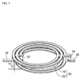
- FIG. 1 illustrates a perspective view of an inductor in accordance with a first comparative embodiment of which the number of turns is 4.5 (a number of turns of a second coil 20 and a first coil 10 is 2.5 and 2 respectively).
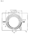
- FIG. 2 illustrates a top view of the inductor.
- the first coil 10 having a spiral shape is provided on a substrate 50 made of glass
- the second coil 20 having a spiral shape is provided on the first coil 10.
- the first coil 10 and the second coil 20 are spaced from each other. A space is formed between the first coil 10 and the second coil 20. That is, air is filled between the first coil 10 and the second coil 20.
- the first coil 10 is almost overlapped with the second coil 20.
- wires 18 and 28 that are made of the same metal layer as the first coil 10 and are configured to be connected to outside of an inductor 30.
- the wire 18 is directly connected to an end of an outermost circumference (that is an outer end) of the first coil 10.
- a third connection portion 34 is provided at an end of an outermost circumference of the second coil 20.
- the wire 28 is electrically coupled to the second coil 20 via the third connection portion 34.
- a first connection portion 32 is provided at an end of innermost circumference (that is an inner end) of the first coil 10 and the second coil 20.
- the first coil 10 and the second coil 20 are electrically coupled to each other via the first connection portion 32.
- the inductor 30 has the first coil 10 and the second coil 20 that are spaced from each other in a longitudinal direction on the substrate 50, are electrically coupled to each other, and have a spiral shape.
- FIG. 3 illustrates a top view of an inductor in accordance with a second comparative embodiment (the first coil 10 is not shown).
- Two fourth connection portions 37 are connected to an inner side face of the innermost circumference of the second coil 20.
- Three second connection portions 38 are connected to an outer side face of the outermost circumference of the second coil 20.
- the second connection portions 38 and the fourth connection portions 37 have the same structure as the first connection portion 32 and the third connection portion 34. Otherwise, the structure of the inductor is as same as that of the first comparative embodiment.
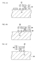
- FIG. 4A through FIG. 4C illustrate a cross sectional view around the first connection portion 32, the third connection portion 34 and the second connection portion 38 respectively.
- the first connection portion 32 is structured with a reception portion 15, a support column 36 and a reception portion 25.
- the support column 36 is formed between the reception portion 15 and the reception portion 25.
- the reception portion 15 is directly connected to the first coil 10.
- the reception portion 25 is directly connected to the second coil 20.
- the third connection portion 34 is structured with the reception portion 15, the support column 36 and the reception portion 25.
- the support column 36 is formed between the reception portion 15 and the reception portion 25.
- the reception portion 15 is directly connected to the wire 28.
- the reception portion 25 is directly connected to the second coil 20.
- the second connection portion 38 is structured with a base portion 23, a support column 24 and the reception portion 25.
- a support column 24 is formed between the base portion 23 and the reception portion 25.
- the reception portion 25 is directly connected to the side face of the second coil 20.
- the base portion 23 is provided on the substrate 50.
- the base portion 23 is not electrically coupled to the wires 18 and 28 and the first coil 10. That is, the second connection portion 38 is provided on the substrate 50 where the wires 18 and 28 or the first coil 10 is not provided.
- the fourth connection portion 37 has the same structure as the second connection portion 38.
- the first coil 10, the wire 28, the reception portion 15 and the base portion 23 are a metal layer that has thickness of approximately 10 ⁇ m and are made of copper formed with a plating method.
- the first coil 10, the wire 28, the reception portion 15 and the base portion 23 are formed together with each other.
- the second coil 20 and the reception portion 25 are a metal layer that has thickness of approximately 10 ⁇ m and are made of copper formed with a plating method.
- the second coil 20 and the reception portion 25 are formed together with each other.
- the second connection portion 38 is made of material that is the same as that of the first connection portion 32 and the third connection portion 34. It is therefore possible to simplify the manufacturing process of forming the second connection portion 38 and the fourth connection portion 37.
- the second connection portion 38 and the fourth connection portion 37 having electrical conductivity are mechanically connected to the side face of the second coil 20 and to the surface of the surface of the substrate 50. It is therefore possible to improve mechanical strength and impact resistance of the second coil 20.
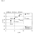
- FIG. 5 illustrates a measured Q value with respect to an inductance value L of the inductors in accordance with the first comparative embodiment and the second comparative embodiment.
- a black circle and a white circle show the first comparative embodiment and the second comparative embodiment respectively.
- the first coil 10 and the second coil 20 of the first comparative embodiment and the second comparative embodiment are made of copper. Thickness T1 of the first coil 10 and thickness T2 of the second coil 20 are approximately 10 ⁇ m. A distance TS between the first coil 10 and the second coil 20 is 30 ⁇ m.
- An inner diameter d of the inductor, a line width W and a line interval S are respectively 250 ⁇ m, 10 ⁇ m and 10 ⁇ m.
- the number R of turns of the inductor 30 is 2.5 to 5.5.
- a measured frequency is 1.93 GHz.
- the Q value of the first comparative embodiment is approximately equal to that of the second comparative embodiment, when the inductance value L is low.
- the Q value of the second comparative embodiment is lower than that of the first comparative embodiment, when the inductance value L is high.
- the Q value of the second comparative embodiment is lower than that of the first comparative embodiment because of eddy-current loss caused by eddy-current generated in the second connection portion 38 and the fourth connection portion 37.
- the fourth connection portion 37 includes an insulator in order to restrain the eddy-current loss, because magnetic flux density of the inner side of the inductor 30 is larger than that of the outer side thereof.
- a support column 24a between the base portion 23 and the reception portion 25 is made of an insulator such as polyimide or BCB (Benzocyclobutene) in a fourth connection portion 37a in accordance with the first embodiment.
- a fourth connection portion 37b is made of an insulator such as polyimide or BCB (Benzocyclobutene) in another version of the first embodiment.
- the fourth connection portion 37b holds the side faces of the second coil 20. It is preferable that a whole of a fourth connection portion 39b is made of insulator as shown in FIG. 6B , from the eddy-current loss viewpoint.
- both of the fourth connection portion(s) 37 and the second connection portion(s) 38 include an insulator.
- Either the second connection portion 38 or the fourth connection portion 37 may, however, include the insulator. It is possible to restrain influence of the eddy-current and support the second coil 20 mechanically if the inner fourth connection portion 37 includes the insulator and the outer second connection portion 38 is conductive from the eddy-current loss view point, because the magnetic field generated by the inductor 30 is larger on the inner side of the inductor 30.
- the substrate 50 is made of highly insulating material in the first embodiment.
- the substrate 50 may be made of an insulating substrate such as quartz (including synthetic quartz), glass (pyrex (registered trademark), tempax, alumino silicate, borosilicate glass) and ceramics, or a high-resistance silicon substrate.
- the substrate 50 may be made of a high-resistance Si substrate, a LiNbO 3 substrate, or a LiTaO 3 substrate.
- the first coil 10 and the second coil 20 are made of low-resistance metal.
- the first coil 10 and the second coil 20 may be made of gold, aluminum, silver in addition to copper.
- the layer of the first coil 10 in touch with the substrate 50 is made of high-melting point metal having high adhesiveness to the substrate, for example metal such as Ti, Cr, Ni, Mo, Ta, W or alloy including at least one of Ti, Cr, Ni, Mo, Ta, W.
- the manufacturing method of the inductor in accordance with the first embodiment may be that of Japanese Patent Application Publication No. 2007-67236 .
- the Q value is reduced when the outer diameter D is reduced.
- the chip size is enlarged when the outer diameter D is enlarged.
- the outer diameter D may be determined in view of the above relations. It is preferable that the outer diameter D is 100 ⁇ m to 1 mm.
- the wire width W may be determined so that the resistance is not enlarged and d/D is not reduced. It is preferable that the wire width W is 3 ⁇ m to 100 ⁇ m.
- the wire interval S may be determined so that wires are inductively connected to each other and the d/D is not reduced. It is preferable that the wire interval S is 3 ⁇ m to 100 ⁇ m.
- the number of turns R may be determined optimally according to the d/D, the wire width W and the wire interval S, and is preferably 0.5 to 30.
- the thickness T1 of the first coil 10 and the thickness T2 of the second coil 20 may be determined in a range where the resistance is not large and the inductor is manufactured easily. It is preferable that the thickness T1 and T2 is 3 ⁇ m to 30 ⁇ m.
- the distance TS between the first coil 10 and the second coil 20 may be determined so that parasitic capacitance is reduced and the inductive connection is enlarged. It is preferable that the distance TS is 3 ⁇ m to 40 ⁇ m.
- FIG. 7 and FIG. 8 illustrate a top view of an inductor in accordance with the second embodiment.
- FIG. 7 illustrates an inductor having the number of turns R of 6.5 (a number of turns of the first coil 10 and the second coil 20 are 3 and 2.5 respectively).
- FIG. 8 illustrates an inductor having the number of turns R of 5.5 (a number of turns of the first coil 10 and the second coil 20 are 3 and 2.5 respectively).
- the fourth connection portion 37 on the inside is not provided.
- FIG. 9 illustrates the Q value with respect to the inductance value L of the inductor in accordance with the first comparative embodiment and the second embodiment. Black dots connected with a solid line indicate the first comparative embodiment. White dots connected with a dashed line indicate the second embodiment.
- the thickness T1 and T2, the distance TS, the wire width W and the wire interval S of the manufactured coil of the second embodiment and the first comparative embodiment are the same as those of the first embodiment.
- FIG. 9 illustrates inductors having the number of turns R of 6.5 to 2.5 and the inner diameter of 125 ⁇ m to 300 ⁇ m at every 25 ⁇ m.
- the Q value is approximately equal in the first comparative embodiment and the second embodiment. This is because eddy current loss is restrained when the second connection portion 38 is not provided inside of the second coil 20 having large magnetic flux density.
- the manufacturing process may be simplified if the first connection portion 32 and the second connection portions 38 are formed together with each other. However, the second connection portion 38 and the fourth connection portion 37 are electrically conductive because the first connection portion 32 is electrically conductive. This results in eddy current loss caused by the second connection portion 38 and the fourth connection portion 37.
- each second connection portion 38 is mechanically connected to the outer side face of the outermost circumference of the second coil 20. No second connection portion 38 is provided inside of the second coil 20.
- the second connection portion 38 is formed on the substrate 50 where the wires 18 and 28 or the first coil 10 is not provided. That is, no second connection portion 38 is provided between the first coil 10 and the second coil 20 (that is the lower face of the second coil 20). It is therefore possible to restrain the eddy current loss.
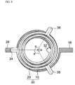
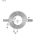
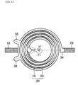
- FIG. 10 and FIG. 11 illustrate a first variant embodiment of the second embodiment.
- FIG. 12 and FIG. 13 illustrate a second variant embodiment of the second embodiment.
- FIG. 10 and FIG. 12 illustrate an inductor having the number of turns R of 6.5.
- FIG. 11 and FIG. 13 illustrate an inductor having the number of turns R of 5.5.
- the second connection portion(s) 38 and the third connection portion 34 are arranged at approximately equal intervals in the second embodiment, as in the case of FIG. 7 and FIG. 8 .
- the angle ⁇ formed with the second connection portion 38 and the third connection portion 34 in the center of the inductor 30 is approximately 180 degrees in the first variant embodiment, as in the case of FIG. 10 and FIG. 11 .
- the second connection portion 38 and the third connection portion 34 are provided at corners opposite each other. As shown in FIG. 12 and FIG. 13 , an angle ⁇ 2 formed between two second connection portions 38 is smaller than an angle ⁇ 1 formed between the third connection portion 34 and each second connection portion 38, in the center of the inductor 30 in the second variant embodiment.
- the two second connection portions 38 are provided adjacent to each other.
- FIG. 14 illustrates a schematic cross sectional view of the inductor.
- the outer portion of the second coil 20 does not move because the outer portion is fixed with the second connection portion 38.
- the inner portion of the second coil 20 moves upward because the inner portion is not fixed with the second connection portion 38.
- a differential between the maximum height and the minimum height of the top face of the second coil 20 is defined as swell U.
- Table 1 and Table 2 show the swell U in cases where the number of turns R is 6.5 and 5.5. As shown in Table 1 and Table 2, the swell U is restrained, when the second connection portion 38 and the third connection portion 34 are arranged on the outer circumference of the second coil 20 at substantially equal intervals as in the case of the second embodiment.
- FIG. 15 illustrates a top view of an inductor in accordance with a third variant embodiment of the second embodiment.
- a wire 28a made of the same metal layer as the second coil 20 is connected to the end of the outermost circumference of the second coil 20.
- the wire 28a is extracted to outside of the second coil 20, and is connected to the wire 28 formed on the substrate 50 with the third connection portion 34.
- the second connection portions 38 provided on the outer side face of the outermost circumference of the second coil 20 are arranged on the outer circumference of the second coil 20 at substantially equal intervals, when the third connection portion 34 is separated from the second coil 20. In this case, the swell U is restrained as in the case of the second embodiment.
- a third embodiment is an example of an integrated passive device having the inductor in accordance with the second embodiment.
- FIG. 16 illustrates a perspective view of the integrated passive device in accordance with the third embodiment.
- FIG. 17 illustrates a top view of the integrated passive device.
- First coils 111 and 121 are not shown in FIG. 17 .
- an inductor 110 having the first coil 111 and a second coil 112 and an inductor 120 having the first coil 121 and a second coil 122.
- the inductors 110 and 120 are each in accordance with the second embodiment.
- the inner end of the first coil 111 and the second coil 112 in the inductor 110 is electrically connected to each other through a first connection portion 165.
- the outer end of the first coil 111 is connected to a wire 152.
- the outer end of the second coil 112 is electrically connected to a wire 151 through a third connection portion 160.
- the second coil 112 is held by a second connection portion 118 at the side face of the outermost circumference thereof.
- the inner end of the first coil 121 and the second coil 122 in the inductor 120 are connected to each other with a first connection portion 175.
- the outer end of the first coil 121 is connected to a wire 154.
- the outer end of the second coil 122 is connected to a wire 153 through a third connection portion 170.
- the second coil 122 is held by a second connection portion 128 at the side face of the outermost circumference thereof.
- the wires 151 through 154 are formed on a substrate 102 and connected to pads 131 through 134 respectively.
- the pad 132 is connected to the pad 133 with a wire 157.
- a capacitor 140 having a lower electrode 141, a dielectric layer 142 and an upper electrode 143 is connected between the pad 131 and the pad 134.
- the upper electrode 143 is connected to the wire 151 with an upper wire 156.
- An integrated passive device 100 forms a ⁇ type L-C-L circuit between the pad 131 and the pad 134, if the pad 131 acts as an input, the pad 134 acts as an output, and the pad 132 and the pad 133 are grounded.
- the inductor 110 and the inductor 120 in the integrated passive device 100 are structured with the inductor in accordance with the second embodiment.
- Mechanical strength and impact resistance of the inductors 110 and 120 may be improved, because the second connection portions 118 and 128 hold the second coils 112 and 122 respectively.
- the swell of the second coil 112 may be restrained, because the two second connection portions 118 and the third connection portion 160 are equally spaced, i.e. arranged at an equal interval.
- the manufacturing process may be simplified because the first connection portion 165, the second connection portion 118 and the third connection portion 160 are formed together with each other.
- the eddy current loss may be restrained because the fourth connection portion is not provided inside of the second coil 112.
Landscapes
- Engineering & Computer Science (AREA)
- Power Engineering (AREA)
- Microelectronics & Electronic Packaging (AREA)
- Coils Or Transformers For Communication (AREA)
- Parts Printed On Printed Circuit Boards (AREA)
Abstract
Description
- The present invention generally relates to an electronic device, and more particularly, to an electronic device having spiral-shaped coils longitudinally spaced from each other.
- An inductor or a capacitor is used for phase matching or the like. For example, there is a demand for downsizing, low cost and high performance in a RF system such as mobile phone or wireless LAN (Local Area Network). An electronic device such as an integrated passive device where passive devices such as an inductor or a capacitor are integrated on a substrate is used in order to satisfy the demand.
- Japanese Patent Application Publication No.
2006-157738 2007-67236 6,518,165 disclose an inductor in which spiral-shaped coils are longitudinally spaced from each other. - In accordance with the inductor disclosed in Japanese Patent Application Publication No.
2007-67236 2007-67236 - The present invention has been made in view of the above circumstances and provides an electronic device having spiral-shaped coils longitudinally spaced from each other, in which the mechanical strength and impact resistance are improved and the inductance property is improved.
- According to an aspect of the present invention, there is provided an electronic device including a substrate, a first coil that has a spiral shape and is provided on the substrate, a second coil that has a spiral shape, is provided above the first coil, and is spaced from the first coil, a first connection portion that electrically couples the first coil and the second coil, a wire that is provided on the substrate and connects one of the first coil and the second coil to the outside, and at least one second connection portion that is mechanically connected to an outer side face of the outermost circumference of the second coil and is mechanically connected on the substrate where one of the wire and the first coil is not provided.
- With the above structure, the mechanical strength and impact resistance of the second coil may be improved because the second coil is mechanically connected to the outside with the second connection portion(s). Inductor characteristics may be improved because the second connection portion is mechanically connected to the outer side face of the outermost circumference of the second coil.
- Reference is made, by way of example only, to the accompanying drawings in which:
-
FIG. 1 illustrates a perspective view of an inductor in accordance with a first comparative embodiment; -
FIG. 2 illustrates a top view of the inductor in accordance with the first comparative embodiment; -
FIG. 3 illustrates a top view of an inductor in accordance with a second comparative embodiment; -
FIG. 4A through FIG. 4C illustrate a cross sectional view of a connection portion in accordance with the second comparative embodiment; -
FIG. 5 illustrates a Q value with respect to L of the inductors in accordance with the first comparative embodiment and the second comparative embodiment; -
FIG. 6A and FIG. 6B illustrate a cross sectional view of the second connection portion in accordance with a first embodiment; -
FIG. 7 illustrates a top view of an inductor in accordance with a second embodiment; -
FIG. 8 illustrates another top view of the inductor in accordance with the second embodiment; -
FIG. 9 illustrates a Q value of L of the inductor in accordance with the second embodiment; -
FIG. 10 illustrates a top view of an inductor in accordance with a first variant of the second embodiment; -
FIG. 11 illustrates another top view of the inductor in accordance with the first variant of the second embodiment; -
FIG. 12 illustrates a top view of an inductor in accordance with a second variant of the second embodiment; -
FIG. 13 illustrates another top view of the inductor in accordance with the second variant of the second embodiment; -
FIG. 14 illustrates a swell of an inductor; -
FIG. 15 illustrates a top view of an inductor in accordance with a third variant of the second embodiment; -
FIG. 16 illustrates a perspective view of an integrated passive device in accordance with a third embodiment; and -
FIG. 17 illustrates a top view of the integrated passive device in accordance with the third embodiment. - In order to facilitate better understanding of the present invention, a description will now be given of related art.
-
FIG. 1 illustrates a perspective view of an inductor in accordance with a first comparative embodiment of which the number of turns is 4.5 (a number of turns of asecond coil 20 and afirst coil 10 is 2.5 and 2 respectively).FIG. 2 illustrates a top view of the inductor. As shown inFIG. 1 andFIG. 2 , thefirst coil 10 having a spiral shape is provided on asubstrate 50 made of glass, and thesecond coil 20 having a spiral shape is provided on thefirst coil 10. Thefirst coil 10 and thesecond coil 20 are spaced from each other. A space is formed between thefirst coil 10 and thesecond coil 20. That is, air is filled between thefirst coil 10 and thesecond coil 20. Thefirst coil 10 is almost overlapped with thesecond coil 20. There are providedwires first coil 10 and are configured to be connected to outside of aninductor 30. Thewire 18 is directly connected to an end of an outermost circumference (that is an outer end) of thefirst coil 10. Athird connection portion 34 is provided at an end of an outermost circumference of thesecond coil 20. Thewire 28 is electrically coupled to thesecond coil 20 via thethird connection portion 34. Afirst connection portion 32 is provided at an end of innermost circumference (that is an inner end) of thefirst coil 10 and thesecond coil 20. Thefirst coil 10 and thesecond coil 20 are electrically coupled to each other via thefirst connection portion 32. Theinductor 30 has thefirst coil 10 and thesecond coil 20 that are spaced from each other in a longitudinal direction on thesubstrate 50, are electrically coupled to each other, and have a spiral shape. -
FIG. 3 illustrates a top view of an inductor in accordance with a second comparative embodiment (thefirst coil 10 is not shown). Twofourth connection portions 37 are connected to an inner side face of the innermost circumference of thesecond coil 20. Threesecond connection portions 38 are connected to an outer side face of the outermost circumference of thesecond coil 20. Thesecond connection portions 38 and thefourth connection portions 37 have the same structure as thefirst connection portion 32 and thethird connection portion 34. Otherwise, the structure of the inductor is as same as that of the first comparative embodiment. -
FIG. 4A through FIG. 4C illustrate a cross sectional view around thefirst connection portion 32, thethird connection portion 34 and thesecond connection portion 38 respectively. As shown inFIG. 4A , thefirst connection portion 32 is structured with areception portion 15, asupport column 36 and areception portion 25. Thesupport column 36 is formed between thereception portion 15 and thereception portion 25. Thereception portion 15 is directly connected to thefirst coil 10. Thereception portion 25 is directly connected to thesecond coil 20. As shown inFIG. 4B , thethird connection portion 34 is structured with thereception portion 15, thesupport column 36 and thereception portion 25. Thesupport column 36 is formed between thereception portion 15 and thereception portion 25. Thereception portion 15 is directly connected to thewire 28. Thereception portion 25 is directly connected to thesecond coil 20. As shown inFIG. 4C , thesecond connection portion 38 is structured with abase portion 23, a support column 24 and thereception portion 25. A support column 24 is formed between thebase portion 23 and thereception portion 25. Thereception portion 25 is directly connected to the side face of thesecond coil 20. Thebase portion 23 is provided on thesubstrate 50. Thebase portion 23 is not electrically coupled to thewires first coil 10. That is, thesecond connection portion 38 is provided on thesubstrate 50 where thewires first coil 10 is not provided. Thefourth connection portion 37 has the same structure as thesecond connection portion 38. - The
first coil 10, thewire 28, thereception portion 15 and thebase portion 23 are a metal layer that has thickness of approximately 10 µm and are made of copper formed with a plating method. Thefirst coil 10, thewire 28, thereception portion 15 and thebase portion 23 are formed together with each other. Thesecond coil 20 and thereception portion 25 are a metal layer that has thickness of approximately 10 µm and are made of copper formed with a plating method. Thesecond coil 20 and thereception portion 25 are formed together with each other. Thesecond connection portion 38 is made of material that is the same as that of thefirst connection portion 32 and thethird connection portion 34. It is therefore possible to simplify the manufacturing process of forming thesecond connection portion 38 and thefourth connection portion 37. - In accordance with the second comparative embodiment, the
second connection portion 38 and thefourth connection portion 37 having electrical conductivity are mechanically connected to the side face of thesecond coil 20 and to the surface of the surface of thesubstrate 50. It is therefore possible to improve mechanical strength and impact resistance of thesecond coil 20. -
FIG. 5 illustrates a measured Q value with respect to an inductance value L of the inductors in accordance with the first comparative embodiment and the second comparative embodiment. A black circle and a white circle show the first comparative embodiment and the second comparative embodiment respectively. Thefirst coil 10 and thesecond coil 20 of the first comparative embodiment and the second comparative embodiment are made of copper. Thickness T1 of thefirst coil 10 and thickness T2 of thesecond coil 20 are approximately 10 µm. A distance TS between thefirst coil 10 and thesecond coil 20 is 30 µm. An inner diameter d of the inductor, a line width W and a line interval S are respectively 250 µm, 10 µm and 10 µm. The number R of turns of theinductor 30 is 2.5 to 5.5. A measured frequency is 1.93 GHz. - As shown in
FIG. 5 , the Q value of the first comparative embodiment is approximately equal to that of the second comparative embodiment, when the inductance value L is low. The Q value of the second comparative embodiment is lower than that of the first comparative embodiment, when the inductance value L is high. The Q value of the second comparative embodiment is lower than that of the first comparative embodiment because of eddy-current loss caused by eddy-current generated in thesecond connection portion 38 and thefourth connection portion 37. - It is preferable that the
fourth connection portion 37 includes an insulator in order to restrain the eddy-current loss, because magnetic flux density of the inner side of theinductor 30 is larger than that of the outer side thereof. As shown inFIG. 6A , a support column 24a between thebase portion 23 and thereception portion 25 is made of an insulator such as polyimide or BCB (Benzocyclobutene) in a fourth connection portion 37a in accordance with the first embodiment. As shown inFIG. 6B , afourth connection portion 37b is made of an insulator such as polyimide or BCB (Benzocyclobutene) in another version of the first embodiment. Thefourth connection portion 37b holds the side faces of thesecond coil 20. It is preferable that a whole of a fourth connection portion 39b is made of insulator as shown inFIG. 6B , from the eddy-current loss viewpoint. - It is preferable that both of the fourth connection portion(s) 37 and the second connection portion(s) 38 include an insulator. Either the
second connection portion 38 or thefourth connection portion 37 may, however, include the insulator. It is possible to restrain influence of the eddy-current and support thesecond coil 20 mechanically if the innerfourth connection portion 37 includes the insulator and the outersecond connection portion 38 is conductive from the eddy-current loss view point, because the magnetic field generated by theinductor 30 is larger on the inner side of theinductor 30. - It is preferable that the
substrate 50 is made of highly insulating material in the first embodiment. Thesubstrate 50 may be made of an insulating substrate such as quartz (including synthetic quartz), glass (pyrex (registered trademark), tempax, alumino silicate, borosilicate glass) and ceramics, or a high-resistance silicon substrate. Thesubstrate 50 may be made of a high-resistance Si substrate, a LiNbO3 substrate, or a LiTaO3 substrate. It is preferable that thefirst coil 10 and thesecond coil 20 are made of low-resistance metal. Thefirst coil 10 and thesecond coil 20 may be made of gold, aluminum, silver in addition to copper. It is preferable that the layer of thefirst coil 10 in touch with thesubstrate 50 is made of high-melting point metal having high adhesiveness to the substrate, for example metal such as Ti, Cr, Ni, Mo, Ta, W or alloy including at least one of Ti, Cr, Ni, Mo, Ta, W. The manufacturing method of the inductor in accordance with the first embodiment may be that of Japanese Patent Application Publication No.2007-67236 - The Q value is reduced when the outer diameter D is reduced. The chip size is enlarged when the outer diameter D is enlarged. The outer diameter D may be determined in view of the above relations. It is preferable that the outer diameter D is 100 µm to 1 mm. The wire width W may be determined so that the resistance is not enlarged and d/D is not reduced. It is preferable that the wire width W is 3 µm to 100 µm. The wire interval S may be determined so that wires are inductively connected to each other and the d/D is not reduced. It is preferable that the wire interval S is 3 µm to 100 µm. The number of turns R may be determined optimally according to the d/D, the wire width W and the wire interval S, and is preferably 0.5 to 30.
- The thickness T1 of the
first coil 10 and the thickness T2 of thesecond coil 20 may be determined in a range where the resistance is not large and the inductor is manufactured easily. It is preferable that the thickness T1 and T2 is 3 µm to 30 µm. The distance TS between thefirst coil 10 and thesecond coil 20 may be determined so that parasitic capacitance is reduced and the inductive connection is enlarged. It is preferable that the distance TS is 3 µm to 40 µm. - A second embodiment is an example where the or each second connection portion is provided only outside of an inductor.
FIG. 7 andFIG. 8 illustrate a top view of an inductor in accordance with the second embodiment.FIG. 7 illustrates an inductor having the number of turns R of 6.5 (a number of turns of thefirst coil 10 and thesecond coil 20 are 3 and 2.5 respectively).FIG. 8 illustrates an inductor having the number of turns R of 5.5 (a number of turns of thefirst coil 10 and thesecond coil 20 are 3 and 2.5 respectively). In the second embodiment, thefourth connection portion 37 on the inside is not provided. There are provided twosecond connection portions 38 on the outside. The angles α formed with the twosecond connection portions 38 and thethird connection portion 34 in the center of theinductor 30 are approximately equal to each other. The structure of thesecond connection portion 38 is the same as that ofFIG. 4C in the first embodiment. That is, the whole of thesecond connection portion 38 is electrically conductive.FIG. 9 illustrates the Q value with respect to the inductance value L of the inductor in accordance with the first comparative embodiment and the second embodiment. Black dots connected with a solid line indicate the first comparative embodiment. White dots connected with a dashed line indicate the second embodiment. The thickness T1 and T2, the distance TS, the wire width W and the wire interval S of the manufactured coil of the second embodiment and the first comparative embodiment are the same as those of the first embodiment.FIG. 9 illustrates inductors having the number of turns R of 6.5 to 2.5 and the inner diameter of 125 µm to 300 µm at every 25 µm. - The Q value is approximately equal in the first comparative embodiment and the second embodiment. This is because eddy current loss is restrained when the
second connection portion 38 is not provided inside of thesecond coil 20 having large magnetic flux density. As shown inFIG. 4A through FIG. 4C , the manufacturing process may be simplified if thefirst connection portion 32 and thesecond connection portions 38 are formed together with each other. However, thesecond connection portion 38 and thefourth connection portion 37 are electrically conductive because thefirst connection portion 32 is electrically conductive. This results in eddy current loss caused by thesecond connection portion 38 and thefourth connection portion 37. In accordance with the second embodiment, eachsecond connection portion 38 is mechanically connected to the outer side face of the outermost circumference of thesecond coil 20. Nosecond connection portion 38 is provided inside of thesecond coil 20. It is therefore possible to restrain the eddy current loss even if thesecond connection portion 38 is electrically conductive. Thesecond connection portion 38 is formed on thesubstrate 50 where thewires first coil 10 is not provided. That is, nosecond connection portion 38 is provided between thefirst coil 10 and the second coil 20 (that is the lower face of the second coil 20). It is therefore possible to restrain the eddy current loss. -
FIG. 10 andFIG. 11 illustrate a first variant embodiment of the second embodiment.FIG. 12 andFIG. 13 illustrate a second variant embodiment of the second embodiment.FIG. 10 andFIG. 12 illustrate an inductor having the number of turns R of 6.5.FIG. 11 andFIG. 13 illustrate an inductor having the number of turns R of 5.5. The second connection portion(s) 38 and thethird connection portion 34 are arranged at approximately equal intervals in the second embodiment, as in the case ofFIG. 7 andFIG. 8 . In contrast, the angle β formed with thesecond connection portion 38 and thethird connection portion 34 in the center of theinductor 30 is approximately 180 degrees in the first variant embodiment, as in the case ofFIG. 10 andFIG. 11 . Thesecond connection portion 38 and thethird connection portion 34 are provided at corners opposite each other. As shown inFIG. 12 andFIG. 13 , an angle γ2 formed between twosecond connection portions 38 is smaller than an angle γ1 formed between thethird connection portion 34 and eachsecond connection portion 38, in the center of theinductor 30 in the second variant embodiment. The twosecond connection portions 38 are provided adjacent to each other. - The
second coil 20 is out of alignment and moves upward because of inner stress thereof, when thesecond coil 20 is formed with a plating method.FIG. 14 illustrates a schematic cross sectional view of the inductor. The outer portion of thesecond coil 20 does not move because the outer portion is fixed with thesecond connection portion 38. The inner portion of thesecond coil 20 moves upward because the inner portion is not fixed with thesecond connection portion 38. A differential between the maximum height and the minimum height of the top face of thesecond coil 20 is defined as swell U. - Table 1 and Table 2 show the swell U in cases where the number of turns R is 6.5 and 5.5. As shown in Table 1 and Table 2, the swell U is restrained, when the
second connection portion 38 and thethird connection portion 34 are arranged on the outer circumference of thesecond coil 20 at substantially equal intervals as in the case of the second embodiment. The swell U is restrained in the case of the first variant embodiment when the number of turns R is 5.5[Table 1] W (µm) S (µm) U (µm) FIRST VARIANT EMBODIMENT 12.5 15 10.09 SECOND VARIANT EMBODIMENT 12.5 15 7.13 SECOND EMBODIMENT 12.5 12.5 4.60 SECOND EMBODIMENT 12.5 15 4.74 SECOND EMBODIMENT 15 12.5 5.62 SECOND EMBODIMENT 15 15 4.96 SECOND EMBODIMENT 17.5 15 4.23 [Table 2] W (µm) S (µm) U (µm) FIRST VARIANT EMBODIMENT 12.5 15 5.26 SECOND VARIANT EMBODIMENT 12.5 15 7.58 SECOND EMBODIMENT 12.5 15 4.96 SECOND EMBODIMENT 15 15 5.69 SECOND EMBODIMENT 17.5 15 5.30 -
FIG. 15 illustrates a top view of an inductor in accordance with a third variant embodiment of the second embodiment. Awire 28a made of the same metal layer as thesecond coil 20 is connected to the end of the outermost circumference of thesecond coil 20. Thewire 28a is extracted to outside of thesecond coil 20, and is connected to thewire 28 formed on thesubstrate 50 with thethird connection portion 34. It is preferable that thesecond connection portions 38 provided on the outer side face of the outermost circumference of thesecond coil 20 are arranged on the outer circumference of thesecond coil 20 at substantially equal intervals, when thethird connection portion 34 is separated from thesecond coil 20. In this case, the swell U is restrained as in the case of the second embodiment. - A third embodiment is an example of an integrated passive device having the inductor in accordance with the second embodiment.
FIG. 16 illustrates a perspective view of the integrated passive device in accordance with the third embodiment.FIG. 17 illustrates a top view of the integrated passive device.First coils 111 and 121 are not shown inFIG. 17 . As shown inFIG. 16 andFIG. 17 , there are provided aninductor 110 having the first coil 111 and asecond coil 112 and aninductor 120 having thefirst coil 121 and asecond coil 122. Theinductors second coil 112 in theinductor 110 is electrically connected to each other through afirst connection portion 165. The outer end of the first coil 111 is connected to awire 152. The outer end of thesecond coil 112 is electrically connected to awire 151 through athird connection portion 160. Thesecond coil 112 is held by asecond connection portion 118 at the side face of the outermost circumference thereof. - The inner end of the
first coil 121 and thesecond coil 122 in theinductor 120 are connected to each other with afirst connection portion 175. The outer end of thefirst coil 121 is connected to awire 154. The outer end of thesecond coil 122 is connected to awire 153 through athird connection portion 170. Thesecond coil 122 is held by asecond connection portion 128 at the side face of the outermost circumference thereof. Thewires 151 through 154 are formed on asubstrate 102 and connected topads 131 through 134 respectively. Thepad 132 is connected to thepad 133 with awire 157. Acapacitor 140 having alower electrode 141, adielectric layer 142 and anupper electrode 143 is connected between thepad 131 and thepad 134. Theupper electrode 143 is connected to thewire 151 with anupper wire 156. An integratedpassive device 100 forms a π type L-C-L circuit between thepad 131 and thepad 134, if thepad 131 acts as an input, thepad 134 acts as an output, and thepad 132 and thepad 133 are grounded. - In accordance with the third embodiment, the
inductor 110 and theinductor 120 in the integratedpassive device 100 are structured with the inductor in accordance with the second embodiment. Mechanical strength and impact resistance of theinductors second connection portions second coils second coil 112 may be restrained, because the twosecond connection portions 118 and thethird connection portion 160 are equally spaced, i.e. arranged at an equal interval. The manufacturing process may be simplified because thefirst connection portion 165, thesecond connection portion 118 and thethird connection portion 160 are formed together with each other. The eddy current loss may be restrained because the fourth connection portion is not provided inside of thesecond coil 112. - The present invention is not limited to the specifically disclosed embodiments, but variations and modifications may be made without departing from the scope of the present invention.
- The present application is based on Japanese Patent Application No.
2007-254662
Claims (9)
- An electronic device comprising:a substrate;a first coil that has a spiral shape and is provided on the substrate;a second coil that has a spiral shape, is provided above the first coil, and is spaced from the first coil;a first connection portion that electrically couples the first coil and the second coil;a wire that is provided on the substrate and connects one of the first coil and the second coil to outside; anda second connection portion that is mechanically connected to an outer side face of outermost circumference of the second coil and is mechanically connected on the substrate where one of the wire and the first coil is not provided.
- The electronic device as claimed in claim 1, wherein the second connection portion is not provided inside of the second coil.
- The electronic device as claimed in claim 1 or 2, wherein the second connection portion is electrically conductive.
- The electronic device as claimed in claim 1, 2, or 3, wherein a plurality of the second connection portions are arranged at substantially equal intervals on the circumference of the second coil.
- The electronic device as claimed in any preceding claim further comprising a third connection portion that is electrically coupled to the wire and the second coil on the substrate and is mechanically connected to the outer side face of the outermost circumference of the second coil,
wherein the second connection portion and the third connection portion are arranged at substantially equal intervals on the circumference of the second coil. - The electronic device as claimed in any preceding claim, wherein the first connection portion and the second connection portion are made of the same material.
- The electronic device as claimed in claim 5, wherein the first connection portion, the second connection portion and the third connection portion are made of the same material.
- The electronic device as claimed in any preceding claim, wherein the second connection portion includes an insulator.
- The electronic device as claimed in any preceding claim further comprising a fourth connection portion that is mechanically connected to an inner side face of innermost circumference of the second coil, is mechanically connected on the substrate where one of the wire and the first coil is not provided, and includes an insulator.
Applications Claiming Priority (1)
| Application Number | Priority Date | Filing Date | Title |
|---|---|---|---|
| JP2007254662A JP5090118B2 (en) | 2007-09-28 | 2007-09-28 | Electronic components |
Publications (3)
| Publication Number | Publication Date |
|---|---|
| EP2043113A2 true EP2043113A2 (en) | 2009-04-01 |
| EP2043113A3 EP2043113A3 (en) | 2012-02-08 |
| EP2043113B1 EP2043113B1 (en) | 2017-10-04 |
Family
ID=40091792
Family Applications (1)
| Application Number | Title | Priority Date | Filing Date |
|---|---|---|---|
| EP08164558.2A Not-in-force EP2043113B1 (en) | 2007-09-28 | 2008-09-18 | Electronic device |
Country Status (4)
| Country | Link |
|---|---|
| US (1) | US7746210B2 (en) |
| EP (1) | EP2043113B1 (en) |
| JP (1) | JP5090118B2 (en) |
| CN (1) | CN101447277B (en) |
Families Citing this family (12)
| Publication number | Priority date | Publication date | Assignee | Title |
|---|---|---|---|---|
| CN104282421A (en) * | 2013-07-03 | 2015-01-14 | 艾默生过程控制流量技术有限公司 | Coil assembly, manufacturing method thereof and on-site instrument |
| KR20170079183A (en) * | 2015-12-30 | 2017-07-10 | 삼성전기주식회사 | Coil Component |
| KR102369430B1 (en) * | 2017-03-15 | 2022-03-03 | 삼성전기주식회사 | Coil electronic component and board having the same |
| KR102581963B1 (en) * | 2017-08-07 | 2023-09-21 | 소니그룹주식회사 | Electronic components, power supplies and vehicles |
| US11605492B2 (en) | 2017-11-13 | 2023-03-14 | Tdk Corporation | Coil component |
| JP7266996B2 (en) * | 2018-11-20 | 2023-05-01 | 太陽誘電株式会社 | Inductors, filters and multiplexers |
| KR102706986B1 (en) * | 2019-04-05 | 2024-09-19 | 삼성전기주식회사 | Coil component |
| KR102335426B1 (en) * | 2020-01-07 | 2021-12-06 | 삼성전기주식회사 | Coil component |
| JP7200956B2 (en) * | 2020-01-27 | 2023-01-10 | 株式会社村田製作所 | inductor components |
| JP2022100882A (en) * | 2020-12-24 | 2022-07-06 | 三安ジャパンテクノロジー株式会社 | Inductor |
| TWI766633B (en) * | 2020-11-18 | 2022-06-01 | 稜研科技股份有限公司 | Broadband linear polarization antenna structure |
| US20230008422A1 (en) * | 2021-07-08 | 2023-01-12 | Smart Prong Technologies, Inc. | Reduction of ac resistive losses in planar conductors |
Citations (4)
| Publication number | Priority date | Publication date | Assignee | Title |
|---|---|---|---|---|
| US6518165B1 (en) | 1998-07-28 | 2003-02-11 | Korea Advanced Institute Of Science And Technology | Method for manufacturing a semiconductor device having a metal layer floating over a substrate |
| JP2006157738A (en) | 2004-11-30 | 2006-06-15 | Fujitsu Media Device Kk | Electronic component and manufacturing method thereof |
| JP2007067236A (en) | 2005-08-31 | 2007-03-15 | Fujitsu Ltd | Integrated electronic component and integrated electronic component manufacturing method |
| JP2007254662A (en) | 2006-03-24 | 2007-10-04 | Teraoka Seisakusho:Kk | Primer coating composition for pressure-sensitive adhesive sheet and pressure-sensitive adhesive sheet produced by using the same |
Family Cites Families (10)
| Publication number | Priority date | Publication date | Assignee | Title |
|---|---|---|---|---|
| JPH05190333A (en) * | 1992-01-13 | 1993-07-30 | Sharp Corp | Multi-layer spiral inductor |
| JPH0955472A (en) * | 1995-08-11 | 1997-02-25 | Mitsubishi Electric Corp | Inductor |
| JP3509362B2 (en) * | 1996-01-26 | 2004-03-22 | シャープ株式会社 | Semiconductor device and manufacturing method thereof |
| GB2321787A (en) * | 1997-01-31 | 1998-08-05 | Nokia Mobile Phones Ltd | Multiple layer printed circuit board inductive arrangement |
| KR100580162B1 (en) * | 1999-10-15 | 2006-05-16 | 삼성전자주식회사 | Thin-film bandpass filter and manufacturing method thereof |
| JP2002043131A (en) * | 2000-07-25 | 2002-02-08 | Taiyo Yuden Co Ltd | Inductance element and its manufacturing method |
| KR100368930B1 (en) * | 2001-03-29 | 2003-01-24 | 한국과학기술원 | Three-Dimensional Metal Devices Highly Suspended above Semiconductor Substrate, Their Circuit Model, and Method for Manufacturing the Same |
| US6972635B2 (en) * | 2002-02-26 | 2005-12-06 | The Regents Of The University Of Michigan | MEMS-based, computer systems, clock generation and oscillator circuits and LC-tank apparatus for use therein |
| JP2004303823A (en) * | 2003-03-28 | 2004-10-28 | Tdk Corp | Inductance components, power transformers and switching power supplies |
| JP2007142157A (en) * | 2005-11-18 | 2007-06-07 | Alps Electric Co Ltd | Variable inductor |
-
2007
- 2007-09-28 JP JP2007254662A patent/JP5090118B2/en active Active
-
2008
- 2008-09-18 EP EP08164558.2A patent/EP2043113B1/en not_active Not-in-force
- 2008-09-25 US US12/237,826 patent/US7746210B2/en active Active
- 2008-09-27 CN CN2008101497957A patent/CN101447277B/en active Active
Patent Citations (4)
| Publication number | Priority date | Publication date | Assignee | Title |
|---|---|---|---|---|
| US6518165B1 (en) | 1998-07-28 | 2003-02-11 | Korea Advanced Institute Of Science And Technology | Method for manufacturing a semiconductor device having a metal layer floating over a substrate |
| JP2006157738A (en) | 2004-11-30 | 2006-06-15 | Fujitsu Media Device Kk | Electronic component and manufacturing method thereof |
| JP2007067236A (en) | 2005-08-31 | 2007-03-15 | Fujitsu Ltd | Integrated electronic component and integrated electronic component manufacturing method |
| JP2007254662A (en) | 2006-03-24 | 2007-10-04 | Teraoka Seisakusho:Kk | Primer coating composition for pressure-sensitive adhesive sheet and pressure-sensitive adhesive sheet produced by using the same |
Also Published As
| Publication number | Publication date |
|---|---|
| EP2043113B1 (en) | 2017-10-04 |
| US20090085707A1 (en) | 2009-04-02 |
| CN101447277A (en) | 2009-06-03 |
| CN101447277B (en) | 2011-11-23 |
| JP5090118B2 (en) | 2012-12-05 |
| JP2009088163A (en) | 2009-04-23 |
| EP2043113A3 (en) | 2012-02-08 |
| US7746210B2 (en) | 2010-06-29 |
Similar Documents
| Publication | Publication Date | Title |
|---|---|---|
| EP2043113B1 (en) | Electronic device | |
| US20090085708A1 (en) | Electronic device | |
| US6037649A (en) | Three-dimension inductor structure in integrated circuit technology | |
| US6480086B1 (en) | Inductor and transformer formed with multi-layer coil turns fabricated on an integrated circuit substrate | |
| US7312685B1 (en) | Symmetrical inductor | |
| US7508291B2 (en) | Inductor element and integrated electronic component | |
| US9412509B2 (en) | Multilayer electronic component having conductive patterns and board having the same | |
| KR102127811B1 (en) | Multilayered electronic component and manufacturing method thereof | |
| US8259459B2 (en) | Electronic device | |
| US7663463B2 (en) | Inductor structure | |
| US12046408B2 (en) | Electronic device and the method to make the same | |
| US7633368B2 (en) | On-chip inductor | |
| JP2019192897A (en) | Inductor | |
| US8722443B2 (en) | Inductor structures for integrated circuit devices | |
| US7312683B1 (en) | Symmetrical inductor | |
| KR101892689B1 (en) | Chip electronic component and board having the same mounted thereon | |
| US20180012697A1 (en) | Coil component | |
| KR20170079183A (en) | Coil Component | |
| CN100511640C (en) | Spiral inductance element with multiple lead structure | |
| US7724116B2 (en) | Symmetrical inductor | |
| CN100442507C (en) | Symmetrical inductance element | |
| US7477125B1 (en) | Symmetrical inductor device | |
| JP5058770B2 (en) | Electronic components | |
| CN111199820B (en) | Inductors, Filters and Multiplexers | |
| CN100416797C (en) | Symmetrical inductance element |
Legal Events
| Date | Code | Title | Description |
|---|---|---|---|
| PUAI | Public reference made under article 153(3) epc to a published international application that has entered the european phase |
Free format text: ORIGINAL CODE: 0009012 |
|
| AK | Designated contracting states |
Kind code of ref document: A2 Designated state(s): AT BE BG CH CY CZ DE DK EE ES FI FR GB GR HR HU IE IS IT LI LT LU LV MC MT NL NO PL PT RO SE SI SK TR |
|
| AX | Request for extension of the european patent |
Extension state: AL BA MK RS |
|
| RAP1 | Party data changed (applicant data changed or rights of an application transferred) |
Owner name: TAIYO YUDEN MOBILE TECHNOLOGY CO., LTD Owner name: FUJITSU LIMITED |
|
| RAP1 | Party data changed (applicant data changed or rights of an application transferred) |
Owner name: FUJITSU LIMITED Owner name: TAIYO YUDEN CO., LTD. |
|
| PUAL | Search report despatched |
Free format text: ORIGINAL CODE: 0009013 |
|
| AK | Designated contracting states |
Kind code of ref document: A3 Designated state(s): AT BE BG CH CY CZ DE DK EE ES FI FR GB GR HR HU IE IS IT LI LT LU LV MC MT NL NO PL PT RO SE SI SK TR |
|
| AX | Request for extension of the european patent |
Extension state: AL BA MK RS |
|
| RIC1 | Information provided on ipc code assigned before grant |
Ipc: H01F 17/00 20060101AFI20120105BHEP Ipc: H01F 27/29 20060101ALI20120105BHEP |
|
| 17P | Request for examination filed |
Effective date: 20120801 |
|
| AKX | Designation fees paid |
Designated state(s): AT BE BG |
|
| REG | Reference to a national code |
Ref country code: DE Ref legal event code: R108 |
|
| RBV | Designated contracting states (corrected) |
Designated state(s): DE FR GB |
|
| REG | Reference to a national code |
Ref country code: DE Ref legal event code: R108 Ref document number: 602008052336 Country of ref document: DE Effective date: 20121017 Ref country code: DE Ref legal event code: R108 Effective date: 20121017 |
|
| 17Q | First examination report despatched |
Effective date: 20150901 |
|
| GRAP | Despatch of communication of intention to grant a patent |
Free format text: ORIGINAL CODE: EPIDOSNIGR1 |
|
| STAA | Information on the status of an ep patent application or granted ep patent |
Free format text: STATUS: GRANT OF PATENT IS INTENDED |
|
| INTG | Intention to grant announced |
Effective date: 20170502 |
|
| RIN1 | Information on inventor provided before grant (corrected) |
Inventor name: MATSUMOTO, TSUYOSHI Inventor name: TAKAHASHI, TAKEO Inventor name: MI, XIAOYU Inventor name: UEDA, SATOSHI |
|
| GRAS | Grant fee paid |
Free format text: ORIGINAL CODE: EPIDOSNIGR3 |
|
| GRAA | (expected) grant |
Free format text: ORIGINAL CODE: 0009210 |
|
| STAA | Information on the status of an ep patent application or granted ep patent |
Free format text: STATUS: THE PATENT HAS BEEN GRANTED |
|
| RIN1 | Information on inventor provided before grant (corrected) |
Inventor name: UEDA, SATOSHI Inventor name: TAKAHASHI, TAKEO Inventor name: MI, XIAOYU Inventor name: MATSUMOTO, TSUYOSHI |
|
| AK | Designated contracting states |
Kind code of ref document: B1 Designated state(s): DE FR GB |
|
| RAP1 | Party data changed (applicant data changed or rights of an application transferred) |
Owner name: FUJITSU LIMITED Owner name: TAIYO YUDEN CO., LTD. |
|
| REG | Reference to a national code |
Ref country code: GB Ref legal event code: FG4D |
|
| REG | Reference to a national code |
Ref country code: DE Ref legal event code: R096 Ref document number: 602008052336 Country of ref document: DE |
|
| REG | Reference to a national code |
Ref country code: DE Ref legal event code: R097 Ref document number: 602008052336 Country of ref document: DE |
|
| REG | Reference to a national code |
Ref country code: FR Ref legal event code: PLFP Year of fee payment: 11 |
|
| PLBE | No opposition filed within time limit |
Free format text: ORIGINAL CODE: 0009261 |
|
| STAA | Information on the status of an ep patent application or granted ep patent |
Free format text: STATUS: NO OPPOSITION FILED WITHIN TIME LIMIT |
|
| 26N | No opposition filed |
Effective date: 20180705 |
|
| PGFP | Annual fee paid to national office [announced via postgrant information from national office to epo] |
Ref country code: FR Payment date: 20190815 Year of fee payment: 12 |
|
| PGFP | Annual fee paid to national office [announced via postgrant information from national office to epo] |
Ref country code: GB Payment date: 20190920 Year of fee payment: 12 |
|
| PGFP | Annual fee paid to national office [announced via postgrant information from national office to epo] |
Ref country code: DE Payment date: 20190903 Year of fee payment: 12 |
|
| REG | Reference to a national code |
Ref country code: DE Ref legal event code: R082 Ref document number: 602008052336 Country of ref document: DE Representative=s name: HL KEMPNER PATENTANWALT, RECHTSANWALT, SOLICIT, DE |
|
| REG | Reference to a national code |
Ref country code: DE Ref legal event code: R119 Ref document number: 602008052336 Country of ref document: DE |
|
| GBPC | Gb: european patent ceased through non-payment of renewal fee |
Effective date: 20200918 |
|
| PG25 | Lapsed in a contracting state [announced via postgrant information from national office to epo] |
Ref country code: DE Free format text: LAPSE BECAUSE OF NON-PAYMENT OF DUE FEES Effective date: 20210401 Ref country code: FR Free format text: LAPSE BECAUSE OF NON-PAYMENT OF DUE FEES Effective date: 20200930 |
|
| PG25 | Lapsed in a contracting state [announced via postgrant information from national office to epo] |
Ref country code: GB Free format text: LAPSE BECAUSE OF NON-PAYMENT OF DUE FEES Effective date: 20200918 |