EP2040518A2 - Heat transfer member and connector - Google Patents
Heat transfer member and connector Download PDFInfo
- Publication number
- EP2040518A2 EP2040518A2 EP08015184A EP08015184A EP2040518A2 EP 2040518 A2 EP2040518 A2 EP 2040518A2 EP 08015184 A EP08015184 A EP 08015184A EP 08015184 A EP08015184 A EP 08015184A EP 2040518 A2 EP2040518 A2 EP 2040518A2
- Authority
- EP
- European Patent Office
- Prior art keywords
- heat
- led
- transfer member
- heat transfer
- conduction metal
- Prior art date
- Legal status (The legal status is an assumption and is not a legal conclusion. Google has not performed a legal analysis and makes no representation as to the accuracy of the status listed.)
- Withdrawn
Links
Images




Classifications
-
- H—ELECTRICITY
- H05—ELECTRIC TECHNIQUES NOT OTHERWISE PROVIDED FOR
- H05K—PRINTED CIRCUITS; CASINGS OR CONSTRUCTIONAL DETAILS OF ELECTRIC APPARATUS; MANUFACTURE OF ASSEMBLAGES OF ELECTRICAL COMPONENTS
- H05K7/00—Constructional details common to different types of electric apparatus
- H05K7/20—Modifications to facilitate cooling, ventilating, or heating
-
- H—ELECTRICITY
- H05—ELECTRIC TECHNIQUES NOT OTHERWISE PROVIDED FOR
- H05K—PRINTED CIRCUITS; CASINGS OR CONSTRUCTIONAL DETAILS OF ELECTRIC APPARATUS; MANUFACTURE OF ASSEMBLAGES OF ELECTRICAL COMPONENTS
- H05K1/00—Printed circuits
- H05K1/02—Details
- H05K1/0201—Thermal arrangements, e.g. for cooling, heating or preventing overheating
- H05K1/0203—Cooling of mounted components
- H05K1/0204—Cooling of mounted components using means for thermal conduction connection in the thickness direction of the substrate
-
- F—MECHANICAL ENGINEERING; LIGHTING; HEATING; WEAPONS; BLASTING
- F21—LIGHTING
- F21V—FUNCTIONAL FEATURES OR DETAILS OF LIGHTING DEVICES OR SYSTEMS THEREOF; STRUCTURAL COMBINATIONS OF LIGHTING DEVICES WITH OTHER ARTICLES, NOT OTHERWISE PROVIDED FOR
- F21V29/00—Protecting lighting devices from thermal damage; Cooling or heating arrangements specially adapted for lighting devices or systems
- F21V29/50—Cooling arrangements
- F21V29/70—Cooling arrangements characterised by passive heat-dissipating elements, e.g. heat-sinks
-
- F—MECHANICAL ENGINEERING; LIGHTING; HEATING; WEAPONS; BLASTING
- F21—LIGHTING
- F21V—FUNCTIONAL FEATURES OR DETAILS OF LIGHTING DEVICES OR SYSTEMS THEREOF; STRUCTURAL COMBINATIONS OF LIGHTING DEVICES WITH OTHER ARTICLES, NOT OTHERWISE PROVIDED FOR
- F21V29/00—Protecting lighting devices from thermal damage; Cooling or heating arrangements specially adapted for lighting devices or systems
- F21V29/50—Cooling arrangements
- F21V29/70—Cooling arrangements characterised by passive heat-dissipating elements, e.g. heat-sinks
- F21V29/74—Cooling arrangements characterised by passive heat-dissipating elements, e.g. heat-sinks with fins or blades
-
- H—ELECTRICITY
- H10—SEMICONDUCTOR DEVICES; ELECTRIC SOLID-STATE DEVICES NOT OTHERWISE PROVIDED FOR
- H10W—GENERIC PACKAGES, INTERCONNECTIONS, CONNECTORS OR OTHER CONSTRUCTIONAL DETAILS OF DEVICES COVERED BY CLASS H10
- H10W40/00—Arrangements for thermal protection or thermal control
- H10W40/20—Arrangements for cooling
- H10W40/25—Arrangements for cooling characterised by their materials
- H10W40/251—Organics
-
- H—ELECTRICITY
- H10—SEMICONDUCTOR DEVICES; ELECTRIC SOLID-STATE DEVICES NOT OTHERWISE PROVIDED FOR
- H10W—GENERIC PACKAGES, INTERCONNECTIONS, CONNECTORS OR OTHER CONSTRUCTIONAL DETAILS OF DEVICES COVERED BY CLASS H10
- H10W40/00—Arrangements for thermal protection or thermal control
- H10W40/20—Arrangements for cooling
- H10W40/25—Arrangements for cooling characterised by their materials
- H10W40/255—Arrangements for cooling characterised by their materials having a laminate or multilayered structure, e.g. direct bond copper [DBC] ceramic substrates
-
- H—ELECTRICITY
- H10—SEMICONDUCTOR DEVICES; ELECTRIC SOLID-STATE DEVICES NOT OTHERWISE PROVIDED FOR
- H10W—GENERIC PACKAGES, INTERCONNECTIONS, CONNECTORS OR OTHER CONSTRUCTIONAL DETAILS OF DEVICES COVERED BY CLASS H10
- H10W40/00—Arrangements for thermal protection or thermal control
- H10W40/70—Fillings or auxiliary members in containers or in encapsulations for thermal protection or control
- H10W40/77—Auxiliary members characterised by their shape
-
- F—MECHANICAL ENGINEERING; LIGHTING; HEATING; WEAPONS; BLASTING
- F21—LIGHTING
- F21K—NON-ELECTRIC LIGHT SOURCES USING LUMINESCENCE; LIGHT SOURCES USING ELECTROCHEMILUMINESCENCE; LIGHT SOURCES USING CHARGES OF COMBUSTIBLE MATERIAL; LIGHT SOURCES USING SEMICONDUCTOR DEVICES AS LIGHT-GENERATING ELEMENTS; LIGHT SOURCES NOT OTHERWISE PROVIDED FOR
- F21K9/00—Light sources using semiconductor devices as light-generating elements, e.g. using light-emitting diodes [LED] or lasers
-
- H—ELECTRICITY
- H05—ELECTRIC TECHNIQUES NOT OTHERWISE PROVIDED FOR
- H05K—PRINTED CIRCUITS; CASINGS OR CONSTRUCTIONAL DETAILS OF ELECTRIC APPARATUS; MANUFACTURE OF ASSEMBLAGES OF ELECTRICAL COMPONENTS
- H05K2201/00—Indexing scheme relating to printed circuits covered by H05K1/00
- H05K2201/01—Dielectrics
- H05K2201/0104—Properties and characteristics in general
- H05K2201/0133—Elastomeric or compliant polymer
-
- H—ELECTRICITY
- H05—ELECTRIC TECHNIQUES NOT OTHERWISE PROVIDED FOR
- H05K—PRINTED CIRCUITS; CASINGS OR CONSTRUCTIONAL DETAILS OF ELECTRIC APPARATUS; MANUFACTURE OF ASSEMBLAGES OF ELECTRICAL COMPONENTS
- H05K2201/00—Indexing scheme relating to printed circuits covered by H05K1/00
- H05K2201/10—Details of components or other objects attached to or integrated in a printed circuit board
- H05K2201/10007—Types of components
- H05K2201/10106—Light emitting diode [LED]
-
- H—ELECTRICITY
- H05—ELECTRIC TECHNIQUES NOT OTHERWISE PROVIDED FOR
- H05K—PRINTED CIRCUITS; CASINGS OR CONSTRUCTIONAL DETAILS OF ELECTRIC APPARATUS; MANUFACTURE OF ASSEMBLAGES OF ELECTRICAL COMPONENTS
- H05K3/00—Apparatus or processes for manufacturing printed circuits
- H05K3/0058—Laminating printed circuit boards onto other substrates, e.g. metallic substrates
- H05K3/0061—Laminating printed circuit boards onto other substrates, e.g. metallic substrates onto a metallic substrate, e.g. a heat sink
Definitions
- This invention relates to a heat transfer member and a connector including the heat transfer member.
- the heat transfer member includes a type made of metal and a type made of resin.
- the heat transfer member made of metal is a spring bent into a substantially L-shape. One end of the spring is brought into contact with an electronic component, and the other end is brought into contact with a heat dissipation member.
- the heat transfer member made of resin is an elastic sheet.
- Heat generated in the electronic component is transferred to the heat dissipation member via the L-shaped spring or the elastic sheet.
- the elastic sheet is made of resin, heat conductivity is low, and therefore, efficiency of heat dissipation is low.
- the L-shaped spring has a problem that heat conductivity is low, due to small contact areas in contact with the electronic component and the heat dissipation member.
- the present invention has been made in view of these circumstances, and an object thereof is to provide a heat transfer member which is capable of enhancing efficiency of heat dissipation, and a connector including the heat transfer member.
- a heat transfer member that transfers heat generated by an electronic component to a heat dissipation member, characterized by comprising an elastic body that is disposed between the electronic component and the heat dissipation member, and a heat conduction metal film that is formed on the elastic body, for transferring heat generated in the electronic component to the heat dissipation member.
- the heat transfer member comprises the elastic body and the heat conduction metal thin film. Therefore, when the heat transfer member is sandwiched between the electronic component and the heat dissipation member, the heat conduction metal film is brought into close contact with the electronic component and the heat dissipation member by the elastic force of the elastic body, whereby the heat generated in the electronic component is transferred to the heat dissipation member via the heat conduction metal film.
- the heat dissipation member comprises a heat sink.
- the heat dissipation member comprises a metal case that accommodates the electronic component.
- the heat dissipation member comprises an electrically conductive pattern for heat dissipation.
- a connector including a heat transfer member that transfers heat generated by an electronic component to a heat dissipation member, characterized in that the heat transfer member comprises an elastic body that is disposed between the electronic component and the heat dissipation member, and a heat conduction metal film that is formed on the elastic body, for transferring heat generated in the electronic component to the heat dissipation member, and that the connector further comprises an electric conduction metal film that electrically connects a terminal section of the electronic component and a pad of a substrate.
- the heat dissipation member comprises a heat sink.
- the heat dissipation member comprises a metal case that accommodates the electronic component.
- the heat dissipation member comprises an electrically conductive pattern for heat dissipation.
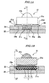
- FIG. 1A is a cross-sectional view, taken on line IA-IA of FIG. 1B , of a heat transfer member according to a first embodiment of the present invention in a state of use.
- FIG. 1B is a cross-sectional view taken on line IB-IB of FIG. 1A .
- a heat transfer member 1 is disposed between an LED (electronic component) 21 and a heat sink (heat dissipation member) 22.
- the LED (light-emitting diode) 21 includes an LED body 21a and a light emitting section 21b.
- the bottom of the LED body 21a has a central part thereof formed with a heat dissipating section 21c.
- Terminal sections 21d are formed on opposite sides of the bottom surface of the LED body 21a, respectively.
- the LED 21 is mounted on a circuit board (substrate) 23.
- the circuit board 23 has a through hole 23a formed therethrough.
- the through hole 23a is opposed to the heat dissipating section 21c of the LED 21 mounted on the circuit board 23.
- two pads 23b are formed on the upper surface of the circuit board 23.
- the pads 23b are disposed in the vicinity of the through hole 23a.
- the terminal sections 21d are fixed to the pads 23b, respectively, by solder 29.
- the heat sink 22 includes numerous fins (not shown) for heat dissipation, and is made of a material having high heat conductivity (e.g., aluminum).
- the heat sink 22 is fixed by an appropriate fixing means, not shown, such as a bolt and nut.
- the heat transfer member lincludes an elastic body 11, a heat conduction metal thin film 12, and a film 13.
- the elastic body 11 is substantially plate-shaped.
- the elastic body 11 is accommodated in the through hole 23a of the circuit board 23, and is disposed between the LED 21 and the heat sink 22.
- the elastic body 11 is sandwiched between the LED 21 and the heat sink 22, and is deformed elastically. Gum or gel is suitable for the material of the elastic body 11.
- the film 13 is affixed to an upper surface to a lower surface of the elastic body 11.
- the heat conduction metal thin film 12 is formed on the film 13.
- the heat conduction metal thin film 12 has one end thereof in contact with the heat dissipating section 21c of the LED 21, and the other end thereof in contact with the heat sink 22.
- the heat conduction metal thin film 12 is formed on the surface of the film 13 by a method of sputtering, vapor deposition, or plating. Au or the like is suitable for the material of the heat conduction metal thin film 12.
- the film 13 is made of a material having insulation properties.
- the heat sink is fixed on the circuit board 23 by a fixing means, beforehand.
- the heat transfer member 1 is inserted into the through hole 23a of the circuit board 23.
- the terminal section 21d of the LED 21 is fixed to the pad 23b of the circuit board 23 by the solder 29.
- the elastic body 11 of the heat transfer member 1 is sandwiched between the LED 21 and the heat sink 22, and is compressed to be elastically deformed.
- the heat conduction metal thin film 12 has one end and the other end thereof pressed against the LED 21 and the heat sink 22, respectively, by the elastic force of the elastic body 11, which makes it possible to secure a large contact area between the heat dissipating section 21c of the LED 21 and the heat conduction metal thin film 12, and also a large contact area between the heat sink 22 and the heat conduction metal thin film 12. Therefore, when the LED 21 generates heat, the heat is efficiently transferred from the LED 21 to the heat sink 22 via the heat conduction metal thin film 12.
- the heat generated in the LED 21 is efficiently transferred to the heat sink 22, it is possible to obtain a high heat dissipation efficiency.
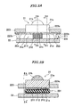
- FIG. 2A is a cross-sectional view, taken on line IIA-IIA of FIG. 2B , of a heat transfer member according to a second embodiment of the present invention in a state of use.
- FIG. 2B is a cross-sectional view taken on line IIB-IIB of FIG. 2A .
- FIG. 2C is a cross-sectional view taken on line IIC-IIC of FIG. 2A .
- the heat transfer member 201 As distinct from the heat transfer member 1 of the first embodiment which has only a function of transferring the heat generated in the LED 21 to the heat sink 22, the heat transfer member 201 according to the second embodiment also has a function of electrically connecting the LED 21 and the circuit board 223, and hence serves both as a heat transfer member and a connector.
- the LED 21 is pressed into a through hole 223a of the circuit board (substrate) 223.
- the circuit board 223 has pads 223b formed on a lower surface thereof. The pads 223b are disposed in the vicinity of the through hole 223a.
- the heat transfer member 201 includes an elastic body 211, a heat conduction metal thin film 212, a electric conduction metal thin film 203, and a film 213.
- the elastic body 211 is substantially plate-shaped, and is larger than the LED 21.
- the film 213 is affixed to an upper surface to a lower surface of the elastic body 211.
- the heat conduction metal thin film 212 is formed on the film 213.
- two belt-shaped electric conduction metal thin films 203 (electric conduction metal films) are formed on the film 213.
- the electric conduction metal thin films 203 are located on opposite sides of the heat conduction metal thin film 212 (see FIG. 2A ).
- the two belt-shaped electric conduction metal thin films 203 are in contact with the associated terminal sections 21d of the LED 21 and the associated pads 223b of the circuit board 223, respectively, whereby the terminal sections 21d and the pads 223b respectively associated therewith are electrically connected.
- the LED 21 is accommodated in the through hole 223a of the circuit board 223, beforehand.
- the heat transfer member 201 is sandwiched between the LED 21 and the heat sink 22.
- the heat sink 22 is fixed on the circuit board 223 by a fixing means, not shown.
- the elastic body 211 is sandwiched between the LED 21 and the heat sink 22, and is compressed to be elastically deformed.
- Each electric conduction metal thin film 203 has one end and the other end thereof pressed against the associated terminal section 21d of the LED 21 and the associated pad 223b of the circuit board 223, respectively, by the elastic force of the elastic body 211. Further, the heat conduction metal thin film 212 has one end and the other end thereof pressed against the heat dissipating section 21c of the LED 21 and the heat sink 22, respectively.
- the electric conduction metal thin film 203 electrically connects between the LED 21 and the circuit board 223 associated therewith, and the heat conduction metal thin film 212 transfers heat generated in the LED 21 to the heat sink 22.
- the same advantageous effects as provided by the first embodiment are obtained, and it is possible to electrically connect the LED 21 and the circuit board 223.
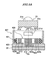
- FIG. 3A is a cross-sectional view, taken on line IIIA--IIIA of FIG. 3B , of a heat transfer member according to a third embodiment of the present invention in a state of use.
- FIG. 3B is a cross-sectional view taken on line IIIB--IIIB of FIG. 3A .
- the third embodiment employs the arrangement for transferring the heat generated in the LED 21 to a metal case (heat dissipation member) 307 and a pad 323c of a conductor pattern (heat dissipation member), not shown, on a circuit board (substrate) 323.
- locking lugs 21e are formed on opposite sides of the LED body 21a of the LED 21.
- the circuit board 323 has pads 323b and 323c formed on an upper surface thereof.
- the conductor pattern on the circuit board 323 connected to the pad 323c extends to outside of the metal case 307 to serve as a heat dissipation member.
- the metal case 307 includes a case body 371 and a fin 372 (see FIG. 3B ).
- the case body is hollow prism-shaped, and has locking holes 371a formed in opposite sides thereof.
- the locking holes 371a receive the locking lugs 21a of the LED 21, whereby the LED 21 is held in the case body 371.
- the fin 372 is connected to the case body 371.
- the fin 372 is in contact with one end of the pad 323c of the circuit board 323.
- the heat transfer member 301 includes an elastic body 311, a heat conduction metal thin film 312, electric conduction metal thin films 303 and 303', and a film 313.
- the heat transfer member 301 has a function of electrically connecting the LED 21 and the circuit board 323, and hence serves both as a heat transfer member and a connector
- the elastic body 311 is substantially plate-shaped, and is larger than the LED 21.
- the elastic body 311 includes an elastic main body 311a, and pressure contact portions 311c.
- the elastic main body 311a is disposed between the LED 21 and the circuit board 323.
- the pressure contact portions 311c are continuous with opposite sides of the elastic main body 311a, i.e. integrally formed with the elastic main body 311a, and are brought into pressure contact with associated inner wall surfaces of the metal case 307.
- the film 313 is affixed to an upper surface to a lower surface of the elastic main body 311a.
- the heat conduction metal thin film 312, which is belt-shaped, is formed on the film 313.
- the heat conduction metal thin film 312 has a width slightly smaller than that of the heat dissipating section 21c of the LED 21.
- the heat conduction metal thin film 312 has one thereof brought into contact with the heat dissipating section 21c of the LED 21, and the other end thereof brought into contact with the fin 372 of the metal case 307.
- the two electric conduction metal thin films (electric conduction metal films) 303 and 303' which are belt-shaped, are formed on the film 313 (see FIG. 3A ).
- the electric conduction metal thin films 303 and 303' are located on opposite sides of the heat conduction metal thin film 312.
- the electric conduction metal thin film 303 is brought into contact with the terminal section 21d of the LED 21 and the pad 323b of the circuit board 323 to electrically connect between the terminal 21d and the pad 323b.
- the electric conduction metal thin film 303' is brought into contact with the terminal section 21d of the LED 21 and the other end of a conductor pattern 323c of the circuit board 323 to electrically connect between the terminal section 21d and the conductor pattern 323c.
- the metal case 307 is fixed on the circuit board 223, beforehand.
- the heat transfer member 301 is inserted into the metal case 307. At this time, since the pressure contact portions 311c are brought into pressure contact with inner wall surfaces of the metal case 307, the heat transfer member 301 is prevented from being wobbly in the metal case 307.
- the LED 21 is inserted into the metal case 307, and the locking lugs 21e of the LED 21 are inserted into the locking holes 371a of the metal case 307 to fix the LED 21 in the metal case 307.
- the elastic main body 311a is sandwiched between the LED 21 and the circuit board 323, an is compressed to be elastically deformed.
- the electric conduction metal thin film 303 has one end and the other end thereof pressed against the terminal section 21d of the LED 21 and the pad 323b of the circuit board 323, respectively, by the elastic force of the elastic main body 311a.
- the electric conduction metal thin film 303' has one end and the other end thereof pressed against the terminal section 21d of the LED 21 and the pad 323c of the circuit board 323, respectively.
- the heat conduction metal thin film 312 has one end thereof pressed against the heat dissipating section 21c, and the other end thereof pressed against the pad 323c of the circuit board 323 via the fin 372.
- the electric conduction metal thin films 303 and 303' electrically connect the LED 21 and the circuit board 323. Further, the heat conduction metal thin film 312 transfers the heat generated in the LED 21 to the case body 371 via the fin 372, and also to the conductor pattern via the fin 372 and the pad 323c of the circuit board 323, for heat dissipation.
- the same advantageous effects as provided by the first and the second embodiments are obtained, and with the provision of the metal case 307, it is possible to more stably hold the LED 21 and the heat transfer member 301.
- a heat transfer member can be envisaged in which the heat generated in the LED 21 is transferred to either the case body 371 or the conductor pattern 323c.
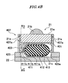
- FIG. 4A is a cross-sectional view, taken on line IVA-IVA of FIG. 4B , of a heat transfer member according to a fourth embodiment of the present invention in a state of use.
- FIG.4B is a cross-sectional view taken on line IVB--IVB of FIG. 4A .
- FIG. 5A is a cross-sectional view, taken on line VA--VA of FIG. 5B , of a state in which an LED is removed from a metal case appearing in FIG. 4A .
- FIG. 5B is a cross-sectional view taken on line VB-VB of FIG. 5A .
- FIG. 6A is a cross-sectional view, taken on line VIA-VIA of FIG. 6B , of a state in which the heat transfer member and the LED are removed from a metal case in FIG. 4A .
- FIG. 6B is a cross-sectional view taken on line VIB-VIB of FIG. 6A .
- the fourth embodiment employs the arrangement for transferring the heat generated in the LED 21 to the heat sink 22.
- a circuit board 423 has a through hole 423a formed through a central part thereof.
- the circuit board 423 has pad 423bs formed on an upper surface thereof. The pads 423b are located in the vicinity of the through hole 423a.
- a metal case 407 has no fin.
- the metal case 407 is square prism-shaped, and has locking holes 407a formed through opposite sides thereof. Locking holes 407a receive locking lugs 21a of the LED 21, whereby the LED 21 is held within the case body 407.
- a heat transfer member 401 includes an elastic body 411, a heat conduction metal thin film 412, electric conduction metal thin films 403, and a film 413.
- the heat transfer member 401 has a function of electrically connecting the LED 21 and the circuit board 423, and hence, the heat transfer member 401 serves both as a heat transfer member and a connector.
- the elastic body 411 is larger than the LED 21, and includes an elastic main body 411a, tabs 411b, and pressure contact portions 411c (see FIGS. 4B and 5B ).
- the elastic main body 411a is located between the LED 21 and the heat sink 22 and has larger thickness than those of the tab 411b and the pressure contact portion 411c.
- the tabs 411b are continuous with the opposite sides of the elastic main body 411a, i.e. integrally formed with the elastic main body 411a, and are located between the LED 21 and the circuit board 423.
- the pressure contact portions 411c are continuous with, i.e. integrally formed with the associated tabs 411b and are brought into pressure contact with inner wall surfaces of the metal case 407.
- the film 413 is affixed to upper surfaces to lower surfaces of the elastic main body 411a and the tabs 411b.
- the heat conduction metal thin film 412 which is belt-shaped, is formed on the film 413. Width of the heat conduction metal thin film 412 is slightly larger than width of the heat dissipating section 21c of the LED 21. One end of the heat conduction metal thin film 412 is brought into contact with the heat dissipating section 21c of the LED 21, and the other end is brought into contact with the heat sink 22.
- the two electric conduction metal thin films (electric conduction metal films) 403, which are belt-shaped, are formed On the film 413.
- the electric conduction metal thin films 403 are located on opposite sides of the heat conduction metal thin film 412.
- the electric conduction metal thin films 403 are each brought into contact with the associated terminal section 21d of the LED 21 and the associated pad 423b of the circuit board 423, to thereby electrically connect the terminal section 21d and the pad 423b.
- the metal case 407 is fixed on the circuit board 423, beforehand.
- the heat transfer member 401 is inserted into the metal case 407. At this time, since the pressure contact portions 411c of the heat transfer member 401 are brought into pressure contact with the inner wall surfaces of the metal case 407, the heat transfer member 401 is prevented from being wobbly in the metal case 407. Further, the lower half portion of the elastic main body 411a of the elastic body 411 is inserted into the through hole 423a of the circuit board 423.
- the LED 21 is inserted into the metal case 407, and the locking lugs 21e of the LED 21 are inserted into locking holes 471a of the metal case 407 to thereby fix the LED 21 in the metal case 407.
- the elastic main body 411a is sandwiched between the LED 21 and the heat sink 22, and is compressed, and the tabs 411b are sandwiched between the LED 21 and the circuit board 423 and are compressed, whereby the elastic main body 411a and the tabs 411b are elastically deformed.
- the heat conduction metal thin film 412 has one end and the other end thereof pressed against the heat dissipating section 21c of the LED 21 and the heat sink 22, respectively, by the elastic force of the elastic main body 411a.
- each metal thin film for heat conduction 403 has one end and the other end thereof pressed against the associated terminal section 21d of the LED 21 and the associated pad 423b of the circuit board 423, respectively, by the elastic force of the associated tab 411b.
- the electric conduction metal thin films 403 electrically connect the LED 21 and the circuit board 423, and the heat conduction metal thin film 412 transfers the heat generated in the LED 21 to the heat sink 22
- a heat transfer member is envisaged in which the metal case 407 is replaced by a case made of a material having a low heat conductivity (e.g. a ceramic material).
- the heat conduction metal thin films 12, 212, 312, and 412 are each formed on the films 13, 213, 313, and 413 affixed to the elastic bodies 11, 211, 311, and 411, respectively, as the heat conduction metal film, the heat conduction metal film is not necessarily required to be a thin film, but it may be a thick film.
- the heat conduction metal thin film may be formed directly on the elastic body.
- the electric conduction metal thin films 203, 303, and 403 are each formed on the films 213, 313, and 413 affixed to the elastic bodies 211, 311, and 411, respectively, as the electric conduction metal film, the electric conduction metal film is not necessarily required to be a thin film, and it may be a thick film or may be foil-shaped.
- the heat conduction metal film may be formed directly on the elastic body.
- each of the films 13, 213, 313, and 413 having the heat conduction metal thin film formed thereon does not cover the whole periphery of the associated one of the elastic bodies 11 211, 311, and 411, as shown in the drawings, so as to make the elastic body easy to be deformed.
- heat transfer members 1, 201, 301, and 401 are intended to perform heat conduction of the LED, the scope of application of the present invention is not limited to the LED, but the present invention may be applied to other electronic components such as a surface-mount type LSIs.
Landscapes
- Engineering & Computer Science (AREA)
- General Engineering & Computer Science (AREA)
- Microelectronics & Electronic Packaging (AREA)
- Physics & Mathematics (AREA)
- Thermal Sciences (AREA)
- Led Device Packages (AREA)
- Cooling Or The Like Of Semiconductors Or Solid State Devices (AREA)
- Arrangement Of Elements, Cooling, Sealing, Or The Like Of Lighting Devices (AREA)
- Cooling Or The Like Of Electrical Apparatus (AREA)
Abstract
Description
- This invention relates to a heat transfer member and a connector including the heat transfer member.
- Conventionally, there has been proposed a heat transfer member which transfers heat generated in electronic components to a heat dissipation member (see Japanese Laid-Open Patent Publication (Kokai) No.
2006-331801 - The heat transfer member includes a type made of metal and a type made of resin.
- The heat transfer member made of metal is a spring bent into a substantially L-shape. One end of the spring is brought into contact with an electronic component, and the other end is brought into contact with a heat dissipation member.
- The heat transfer member made of resin is an elastic sheet.
- Heat generated in the electronic component is transferred to the heat dissipation member via the L-shaped spring or the elastic sheet.
- However, since the elastic sheet is made of resin, heat conductivity is low, and therefore, efficiency of heat dissipation is low.
- Further, the L-shaped spring has a problem that heat conductivity is low, due to small contact areas in contact with the electronic component and the heat dissipation member.
- The present invention has been made in view of these circumstances, and an object thereof is to provide a heat transfer member which is capable of enhancing efficiency of heat dissipation, and a connector including the heat transfer member.
- To attain the above object, in a first aspect of the present invention, there is provided a heat transfer member that transfers heat generated by an electronic component to a heat dissipation member, characterized by comprising an elastic body that is disposed between the electronic component and the heat dissipation member, and a heat conduction metal film that is formed on the elastic body, for transferring heat generated in the electronic component to the heat dissipation member.
- With the arrangement of the heat transfer member according to the first aspect of the present invention, the heat transfer member comprises the elastic body and the heat conduction metal thin film. Therefore, when the heat transfer member is sandwiched between the electronic component and the heat dissipation member, the heat conduction metal film is brought into close contact with the electronic component and the heat dissipation member by the elastic force of the elastic body, whereby the heat generated in the electronic component is transferred to the heat dissipation member via the heat conduction metal film.
- According to the first aspect of the present invention, it is possible to enhance efficiency of heat dissipation.
- Preferably, the heat dissipation member comprises a heat sink.
- Preferably, the heat dissipation member comprises a metal case that accommodates the electronic component.
- Preferably, the heat dissipation member comprises an electrically conductive pattern for heat dissipation.
- To attain the above object, in a second aspect of the present invention, there is provided a connector including a heat transfer member that transfers heat generated by an electronic component to a heat dissipation member, characterized in that the heat transfer member comprises an elastic body that is disposed between the electronic component and the heat dissipation member, and a heat conduction metal film that is formed on the elastic body, for transferring heat generated in the electronic component to the heat dissipation member, and that the connector further comprises an electric conduction metal film that electrically connects a terminal section of the electronic component and a pad of a substrate.
- According to the second aspect of the present invention, it is possible to obtain the same advantageous effects as provided by the first aspect of the present invention.
- Preferably, the heat dissipation member comprises a heat sink.
- Preferably, the heat dissipation member comprises a metal case that accommodates the electronic component.
- Preferably, the heat dissipation member comprises an electrically conductive pattern for heat dissipation.
- The above and other objects, features and advantages of the present invention will become more apparent from the following detailed description taken in conjunction with the accompanying drawings.
-
-
FIG. 1A is a cross-sectional view, taken on line IA--IA ofFIG. 1B , of a heat transfer member according to a first embodiment of the present invention in a state of use; -
FIG. 1B is a cross-sectional view taken on line IB--IB ofFIG. 1A ; -
FIG. 2A is a cross-sectional view, taken on line IIA---IIA ofFIG. 2B , of a heat transfer member according to a second embodiment of the present invention in a state of use; -
FIG. 2B is a cross-sectional view taken on line IIB--IIB ofFIG. 2A ; -
FIG. 2C is a cross-sectional view taken on line IIC--IIC ofFIG. 2A ; -
FIG. 3A is a cross-sectional view, taken on line IIIA---IIIA ofFIG. 3B , of a heat transfer member according to a third embodiment of the present invention in a state of use; -
FIG. 3B is a cross-sectional view taken on line IIIB--IIIB ofFIG. 3A ; -
FIG. 4A is a cross-sectional view, taken on line IVA--IVA ofFIG. 4B , of a heat transfer member according to a fourth embodiment of the present invention in a state of use; -
FIG.4B is a cross-sectional view taken on line IV B--IVB ofFIG. 4A ; -
FIG. 5A is a cross-sectional view, taken on line VA--VA ofFIG. 5B , of a state in which an LED is removed from a metal case appearing inFIG. 4A ; -
FIG. 5B is a cross-sectional view taken on line VB--VB ofFIG. 5A ; -
FIG. 6A is a cross-sectional view, taken on line VIA--VIA ofFIG. 6B , of a state in which the heat transfer member and the LED are removed from the metal case appearing inFIG. 4A ; and -
FIG. 6B is a cross-sectional view taken on line VIB--VIB ofFIG. 6A ; - The present invention will now be described in detail with reference to the drawings showing preferred embodiments thereof.
-
FIG. 1A is a cross-sectional view, taken on line IA-IA ofFIG. 1B , of a heat transfer member according to a first embodiment of the present invention in a state of use.FIG. 1B is a cross-sectional view taken on line IB-IB ofFIG. 1A . - As shown in
FIGS. 1A and 1B , aheat transfer member 1 is disposed between an LED (electronic component) 21 and a heat sink (heat dissipation member) 22. - The LED (light-emitting diode) 21 includes an
LED body 21a and alight emitting section 21b. The bottom of theLED body 21a has a central part thereof formed with aheat dissipating section 21c.Terminal sections 21d are formed on opposite sides of the bottom surface of theLED body 21a, respectively. - The
LED 21 is mounted on a circuit board (substrate) 23. Thecircuit board 23 has a throughhole 23a formed therethrough. The throughhole 23a is opposed to theheat dissipating section 21c of theLED 21 mounted on thecircuit board 23. Further, twopads 23b are formed on the upper surface of thecircuit board 23. Thepads 23b are disposed in the vicinity of the throughhole 23a. Theterminal sections 21d are fixed to thepads 23b, respectively, bysolder 29. - The
heat sink 22 includes numerous fins (not shown) for heat dissipation, and is made of a material having high heat conductivity (e.g., aluminum). - As shown in
FIG. 1B , theheat sink 22 is fixed by an appropriate fixing means, not shown, such as a bolt and nut. - The heat transfer member lincludes an
elastic body 11, a heat conduction metalthin film 12, and afilm 13. - The
elastic body 11 is substantially plate-shaped. Theelastic body 11 is accommodated in the throughhole 23a of thecircuit board 23, and is disposed between theLED 21 and theheat sink 22. Theelastic body 11 is sandwiched between theLED 21 and theheat sink 22, and is deformed elastically. Gum or gel is suitable for the material of theelastic body 11. - The
film 13 is affixed to an upper surface to a lower surface of theelastic body 11. The heat conduction metalthin film 12 is formed on thefilm 13. The heat conduction metalthin film 12 has one end thereof in contact with theheat dissipating section 21c of theLED 21, and the other end thereof in contact with theheat sink 22. - The heat conduction metal
thin film 12 is formed on the surface of thefilm 13 by a method of sputtering, vapor deposition, or plating. Au or the like is suitable for the material of the heat conduction metalthin film 12. - The
film 13 is made of a material having insulation properties. - Next, a description will be given of how the
heat transfer member 1 is used. - To dispose the
heat transfer member 1 between theLED 21 and theheat sink 22, the heat sink is fixed on thecircuit board 23 by a fixing means, beforehand. - First, the
heat transfer member 1 is inserted into the throughhole 23a of thecircuit board 23. - Next, the
terminal section 21d of theLED 21 is fixed to thepad 23b of thecircuit board 23 by thesolder 29. - At this time, the
elastic body 11 of theheat transfer member 1 is sandwiched between theLED 21 and theheat sink 22, and is compressed to be elastically deformed. - The heat conduction metal
thin film 12 has one end and the other end thereof pressed against theLED 21 and theheat sink 22, respectively, by the elastic force of theelastic body 11, which makes it possible to secure a large contact area between theheat dissipating section 21c of theLED 21 and the heat conduction metalthin film 12, and also a large contact area between theheat sink 22 and the heat conduction metalthin film 12. Therefore, when theLED 21 generates heat, the heat is efficiently transferred from theLED 21 to theheat sink 22 via the heat conduction metalthin film 12. - According to the first embodiment, since the heat generated in the
LED 21 is efficiently transferred to theheat sink 22, it is possible to obtain a high heat dissipation efficiency. -
FIG. 2A is a cross-sectional view, taken on line IIA-IIA ofFIG. 2B , of a heat transfer member according to a second embodiment of the present invention in a state of use.FIG. 2B is a cross-sectional view taken on line IIB-IIB ofFIG. 2A .FIG. 2C is a cross-sectional view taken on line IIC-IIC ofFIG. 2A . - Component parts identical to those of the according to the first embodiment are designated by identical reference numerals, and detailed description thereof is omitted, while only main component parts different in construction from those of the first embodiment will be described hereinafter.
- As distinct from the
heat transfer member 1 of the first embodiment which has only a function of transferring the heat generated in theLED 21 to theheat sink 22, theheat transfer member 201 according to the second embodiment also has a function of electrically connecting theLED 21 and thecircuit board 223, and hence serves both as a heat transfer member and a connector. - AS shown in
FIGS. 2A and 2B , theLED 21 is pressed into a throughhole 223a of the circuit board (substrate) 223. Thecircuit board 223 haspads 223b formed on a lower surface thereof. Thepads 223b are disposed in the vicinity of the throughhole 223a. - The
heat transfer member 201 includes anelastic body 211, a heat conduction metalthin film 212, a electric conduction metalthin film 203, and afilm 213. - The
elastic body 211 is substantially plate-shaped, and is larger than theLED 21. - The
film 213 is affixed to an upper surface to a lower surface of theelastic body 211. The heat conduction metalthin film 212 is formed on thefilm 213. - On the
film 213, two belt-shaped electric conduction metal thin films 203 (electric conduction metal films) are formed. The electric conduction metalthin films 203 are located on opposite sides of the heat conduction metal thin film 212 (seeFIG. 2A ). The two belt-shaped electric conduction metalthin films 203 are in contact with the associatedterminal sections 21d of theLED 21 and the associatedpads 223b of thecircuit board 223, respectively, whereby theterminal sections 21d and thepads 223b respectively associated therewith are electrically connected. - Next, a description will be given of how the
heat transfer member 201 is used. - To dispose the
heat transfer member 201 between theLED 21 and theheat sink 22, theLED 21 is accommodated in the throughhole 223a of thecircuit board 223, beforehand. - First, the
heat transfer member 201 is sandwiched between theLED 21 and theheat sink 22. - Next, the
heat sink 22 is fixed on thecircuit board 223 by a fixing means, not shown. - At this time, the
elastic body 211 is sandwiched between theLED 21 and theheat sink 22, and is compressed to be elastically deformed. - Each electric conduction metal
thin film 203 has one end and the other end thereof pressed against the associatedterminal section 21d of theLED 21 and the associatedpad 223b of thecircuit board 223, respectively, by the elastic force of theelastic body 211. Further, the heat conduction metalthin film 212 has one end and the other end thereof pressed against theheat dissipating section 21c of theLED 21 and theheat sink 22, respectively. - As a result, the electric conduction metal
thin film 203 electrically connects between theLED 21 and thecircuit board 223 associated therewith, and the heat conduction metalthin film 212 transfers heat generated in theLED 21 to theheat sink 22. - According to the second embodiment, the same advantageous effects as provided by the first embodiment are obtained, and it is possible to electrically connect the
LED 21 and thecircuit board 223. -
FIG. 3A is a cross-sectional view, taken on line IIIA--IIIA ofFIG. 3B , of a heat transfer member according to a third embodiment of the present invention in a state of use.FIG. 3B is a cross-sectional view taken on line IIIB--IIIB ofFIG. 3A . - Component parts identical to those of the according to the first and second embodiments are designated by identical reference numerals, and detailed description thereof is omitted, while only main component parts different in construction from those of the second embodiment will be described hereinafter.
- As distinct from the second embodiment which employs the arrangement for transferring heat generated in the
LED 21 to theheat sink 22, the third embodiment employs the arrangement for transferring the heat generated in theLED 21 to a metal case (heat dissipation member) 307 and apad 323c of a conductor pattern (heat dissipation member), not shown, on a circuit board (substrate) 323. - As shown in
FIGS. 3A and3B , lockinglugs 21e are formed on opposite sides of theLED body 21a of theLED 21. - The
circuit board 323 haspads circuit board 323 connected to thepad 323c extends to outside of themetal case 307 to serve as a heat dissipation member. - The
metal case 307 includes acase body 371 and a fin 372 (seeFIG. 3B ). The case body is hollow prism-shaped, and has lockingholes 371a formed in opposite sides thereof. The lockingholes 371a receive the locking lugs 21a of theLED 21, whereby theLED 21 is held in thecase body 371. - The
fin 372 is connected to thecase body 371. Thefin 372 is in contact with one end of thepad 323c of thecircuit board 323. - The
heat transfer member 301 includes anelastic body 311, a heat conduction metalthin film 312, electric conduction metal thin films 303 and 303', and afilm 313. Theheat transfer member 301 has a function of electrically connecting theLED 21 and thecircuit board 323, and hence serves both as a heat transfer member and a connector - The
elastic body 311 is substantially plate-shaped, and is larger than theLED 21. Theelastic body 311 includes an elasticmain body 311a, andpressure contact portions 311c. The elasticmain body 311a is disposed between theLED 21 and thecircuit board 323. Thepressure contact portions 311c are continuous with opposite sides of the elasticmain body 311a, i.e. integrally formed with the elasticmain body 311a, and are brought into pressure contact with associated inner wall surfaces of themetal case 307. - The
film 313 is affixed to an upper surface to a lower surface of the elasticmain body 311a. The heat conduction metalthin film 312, which is belt-shaped, is formed on thefilm 313. The heat conduction metalthin film 312 has a width slightly smaller than that of theheat dissipating section 21c of theLED 21. The heat conduction metalthin film 312 has one thereof brought into contact with theheat dissipating section 21c of theLED 21, and the other end thereof brought into contact with thefin 372 of themetal case 307. - The two electric conduction metal thin films (electric conduction metal films) 303 and 303', which are belt-shaped, are formed on the film 313 (see
FIG. 3A ). The electric conduction metal thin films 303 and 303' are located on opposite sides of the heat conduction metalthin film 312. The electric conduction metal thin film 303 is brought into contact with theterminal section 21d of theLED 21 and thepad 323b of thecircuit board 323 to electrically connect between the terminal 21d and thepad 323b. The electric conduction metal thin film 303' is brought into contact with theterminal section 21d of theLED 21 and the other end of aconductor pattern 323c of thecircuit board 323 to electrically connect between theterminal section 21d and theconductor pattern 323c. - Next, a description will be given of how the
heat transfer member 301 is used. - To dispose the
heat transfer member 301 between theLED 21 and thecircuit board 323, themetal case 307 is fixed on thecircuit board 223, beforehand. - First, the
heat transfer member 301 is inserted into themetal case 307. At this time, since thepressure contact portions 311c are brought into pressure contact with inner wall surfaces of themetal case 307, theheat transfer member 301 is prevented from being wobbly in themetal case 307. - Next, the
LED 21 is inserted into themetal case 307, and the locking lugs 21e of theLED 21 are inserted into the lockingholes 371a of themetal case 307 to fix theLED 21 in themetal case 307. - At this time, the elastic
main body 311a is sandwiched between theLED 21 and thecircuit board 323, an is compressed to be elastically deformed. - The electric conduction metal thin film 303 has one end and the other end thereof pressed against the
terminal section 21d of theLED 21 and thepad 323b of thecircuit board 323, respectively, by the elastic force of the elasticmain body 311a. The electric conduction metal thin film 303' has one end and the other end thereof pressed against theterminal section 21d of theLED 21 and thepad 323c of thecircuit board 323, respectively. Further, the heat conduction metalthin film 312 has one end thereof pressed against theheat dissipating section 21c, and the other end thereof pressed against thepad 323c of thecircuit board 323 via thefin 372. - As a result, the electric conduction metal thin films 303 and 303' electrically connect the
LED 21 and thecircuit board 323. Further, the heat conduction metalthin film 312 transfers the heat generated in theLED 21 to thecase body 371 via thefin 372, and also to the conductor pattern via thefin 372 and thepad 323c of thecircuit board 323, for heat dissipation. - According to the third embodiment, the same advantageous effects as provided by the first and the second embodiments are obtained, and with the provision of the
metal case 307, it is possible to more stably hold theLED 21 and theheat transfer member 301. - As a variation of the third embodiment, a heat transfer member can be envisaged in which the heat generated in the
LED 21 is transferred to either thecase body 371 or theconductor pattern 323c. -
FIG. 4A is a cross-sectional view, taken on line IVA-IVA ofFIG. 4B , of a heat transfer member according to a fourth embodiment of the present invention in a state of use.FIG.4B is a cross-sectional view taken on line IVB--IVB ofFIG. 4A .FIG. 5A is a cross-sectional view, taken on line VA--VA ofFIG. 5B , of a state in which an LED is removed from a metal case appearing inFIG. 4A .FIG. 5B is a cross-sectional view taken on line VB-VB ofFIG. 5A .FIG. 6A is a cross-sectional view, taken on line VIA-VIA ofFIG. 6B , of a state in which the heat transfer member and the LED are removed from a metal case inFIG. 4A .FIG. 6B is a cross-sectional view taken on line VIB-VIB ofFIG. 6A . - Component parts identical to those of the according to the first and third embodiments are designated by identical reference numerals, and detailed description thereof is omitted, while only main component parts different in construction from those of the first and third embodiments will be described hereinafter.
- As distinct from the third embodiment which employs the arrangement for transferring the heat generated in the
LED 21 to themetal case 307 and the conductor pattern, the fourth embodiment employs the arrangement for transferring the heat generated in theLED 21 to theheat sink 22. - As shown in
FIGS. 4A ,4B ,5A , and5B , acircuit board 423 has a throughhole 423a formed through a central part thereof. Thecircuit board 423 has pad 423bs formed on an upper surface thereof. Thepads 423b are located in the vicinity of the throughhole 423a. - As shown in
FIGS. 6A and6B , ametal case 407 has no fin. Themetal case 407 is square prism-shaped, and has lockingholes 407a formed through opposite sides thereof. Lockingholes 407a receive lockinglugs 21a of theLED 21, whereby theLED 21 is held within thecase body 407. - As shown in
FIGS. 4A ,4B ,5A , and5B , aheat transfer member 401 includes anelastic body 411, a heat conduction metalthin film 412, electric conduction metalthin films 403, and afilm 413. Theheat transfer member 401 has a function of electrically connecting theLED 21 and thecircuit board 423, and hence, theheat transfer member 401 serves both as a heat transfer member and a connector. - The
elastic body 411 is larger than theLED 21, and includes an elasticmain body 411a,tabs 411b, andpressure contact portions 411c (seeFIGS. 4B and5B ). The elasticmain body 411a is located between theLED 21 and theheat sink 22 and has larger thickness than those of thetab 411b and thepressure contact portion 411c. Thetabs 411b are continuous with the opposite sides of the elasticmain body 411a, i.e. integrally formed with the elasticmain body 411a, and are located between theLED 21 and thecircuit board 423. Thepressure contact portions 411c are continuous with, i.e. integrally formed with the associatedtabs 411b and are brought into pressure contact with inner wall surfaces of themetal case 407. - The
film 413 is affixed to upper surfaces to lower surfaces of the elasticmain body 411a and thetabs 411b. The heat conduction metalthin film 412, which is belt-shaped, is formed on thefilm 413. Width of the heat conduction metalthin film 412 is slightly larger than width of theheat dissipating section 21c of theLED 21. One end of the heat conduction metalthin film 412 is brought into contact with theheat dissipating section 21c of theLED 21, and the other end is brought into contact with theheat sink 22. - The two electric conduction metal thin films (electric conduction metal films) 403, which are belt-shaped, are formed On the
film 413. The electric conduction metalthin films 403 are located on opposite sides of the heat conduction metalthin film 412. The electric conduction metalthin films 403 are each brought into contact with the associatedterminal section 21d of theLED 21 and the associatedpad 423b of thecircuit board 423, to thereby electrically connect theterminal section 21d and thepad 423b. - Next, a description will be given of how the
heat transfer member 401 is used. - To dispose the
heat transfer member 401 between theLED 21 and thecircuit board 423, themetal case 407 is fixed on thecircuit board 423, beforehand. - First, the
heat transfer member 401 is inserted into themetal case 407. At this time, since thepressure contact portions 411c of theheat transfer member 401 are brought into pressure contact with the inner wall surfaces of themetal case 407, theheat transfer member 401 is prevented from being wobbly in themetal case 407. Further, the lower half portion of the elasticmain body 411a of theelastic body 411 is inserted into the throughhole 423a of thecircuit board 423. - ]Next, the
LED 21 is inserted into themetal case 407, and the locking lugs 21e of theLED 21 are inserted into locking holes 471a of themetal case 407 to thereby fix theLED 21 in themetal case 407. - At this time, the elastic
main body 411a is sandwiched between theLED 21 and theheat sink 22, and is compressed, and thetabs 411b are sandwiched between theLED 21 and thecircuit board 423 and are compressed, whereby the elasticmain body 411a and thetabs 411b are elastically deformed. - The heat conduction metal
thin film 412 has one end and the other end thereof pressed against theheat dissipating section 21c of theLED 21 and theheat sink 22, respectively, by the elastic force of the elasticmain body 411a. - Further, each metal thin film for
heat conduction 403 has one end and the other end thereof pressed against the associatedterminal section 21d of theLED 21 and the associatedpad 423b of thecircuit board 423, respectively, by the elastic force of the associatedtab 411b. - As a result, the electric conduction metal
thin films 403 electrically connect theLED 21 and thecircuit board 423, and the heat conduction metalthin film 412 transfers the heat generated in theLED 21 to theheat sink 22 - According to the fourth embodiment, the same advantageous effects as provided by the third embodiment are obtained.
- As a variation of the fourth embodiment, a heat transfer member is envisaged in which the
metal case 407 is replaced by a case made of a material having a low heat conductivity (e.g. a ceramic material). - According to the variation, it is possible to transfer the heat generated in the
LED 21 to theheat sink 22 in a concentrated manner. - It should be noted that although in the above-described embodiments, the heat conduction metal
thin films films elastic bodies - Further, the heat conduction metal thin film may be formed directly on the elastic body.
- It should be noted that although in the above-described embodiments, the electric conduction metal
thin films films elastic bodies - Further, the heat conduction metal film may be formed directly on the elastic body.
- According to the above-described embodiments, each of the
films elastic bodies 11 211, 311, and 411, as shown in the drawings, so as to make the elastic body easy to be deformed. - It should be noted that although the
heat transfer members - It is further understood by those skilled in the art that the foregoing are the preferred embodiments of the present invention, and that various changes and modification may be made thereto without departing from the spirit and scope thereof.
Claims (5)
- A heat transfer member that transfers heat generated by an electronic component to a heat dissipation member,
characterized by comprising:an elastic body that is disposed between the electronic component and the heat dissipation member; anda heat conduction metal film that is formed on said elastic body, for transferring heat generated in the electronic component to the heat dissipation member. - A heat transfer member as claimed in claim 1, wherein the heat dissipation member comprises a heat sink.
- A heat transfer member as claimed in claim 1, wherein the heat dissipation member comprises a metal case that accommodates the electronic component.
- A heat transfer member as claimed in claim 1, wherein the heat dissipation member comprises an electrically conductive pattern for heat dissipation.
- A connector including a heat transfer member as claimed in any preceding claim, wherein
the connector further comprises an electric conduction metal film that electrically connects a terminal section of the electronic component and a pad of a substrate.
Applications Claiming Priority (1)
| Application Number | Priority Date | Filing Date | Title |
|---|---|---|---|
| JP2007240503 | 2007-09-18 |
Publications (2)
| Publication Number | Publication Date |
|---|---|
| EP2040518A2 true EP2040518A2 (en) | 2009-03-25 |
| EP2040518A3 EP2040518A3 (en) | 2012-03-28 |
Family
ID=40259125
Family Applications (1)
| Application Number | Title | Priority Date | Filing Date |
|---|---|---|---|
| EP08015184A Withdrawn EP2040518A3 (en) | 2007-09-18 | 2008-08-28 | Heat transfer member and connector |
Country Status (6)
| Country | Link |
|---|---|
| US (1) | US7766661B2 (en) |
| EP (1) | EP2040518A3 (en) |
| JP (1) | JP4570106B2 (en) |
| KR (1) | KR101102707B1 (en) |
| CN (1) | CN101394052B (en) |
| TW (1) | TWI376071B (en) |
Families Citing this family (27)
| Publication number | Priority date | Publication date | Assignee | Title |
|---|---|---|---|---|
| JP2009200187A (en) * | 2008-02-21 | 2009-09-03 | Kamakura Denshi Kogyo Kk | Led mounting method of lighting system, and led lighting system |
| JP5320181B2 (en) * | 2009-06-19 | 2013-10-23 | 日本航空電子工業株式会社 | Electrical connection member and socket connector using the same |
| US20100321893A1 (en) * | 2009-06-20 | 2010-12-23 | Peter Scott Andrews | Heat Dissipation Packaging for Electrical Components |
| US20110249406A1 (en) * | 2009-06-20 | 2011-10-13 | LEDAdventures LLC | Heat dissipation system for electrical components |
| US8622579B2 (en) | 2009-06-29 | 2014-01-07 | Seoul Semiconductor Co., Ltd. | Illumination system |
| KR20110002892A (en) * | 2009-06-29 | 2011-01-11 | 서울반도체 주식회사 | Light emitting module |
| TW201119105A (en) * | 2009-11-30 | 2011-06-01 | Li Hong Science & Technology Co Ltd | LED heat conductive seat and manufacturing process thereof |
| JP2011204599A (en) * | 2010-03-26 | 2011-10-13 | Panasonic Electric Works Co Ltd | Socket for memory card |
| CN201706335U (en) * | 2010-05-28 | 2011-01-12 | 陈烱勋 | LED Street Light |
| CN101881393A (en) * | 2010-07-06 | 2010-11-10 | 中国计量学院 | A LED lamp structure using metal substrate and metal solder to conduct heat |
| US10433414B2 (en) * | 2010-12-24 | 2019-10-01 | Rayben Technologies (HK) Limited | Manufacturing method of printing circuit board with micro-radiators |
| KR101824038B1 (en) * | 2011-07-22 | 2018-01-31 | 엘지이노텍 주식회사 | display apparatus |
| CN102958323A (en) * | 2011-08-29 | 2013-03-06 | 佳能企业股份有限公司 | Heat conducting structure |
| TW201320877A (en) * | 2011-11-04 | 2013-05-16 | 茂晶國際能源股份有限公司 | Thermal management device and electronic device |
| WO2013080442A1 (en) * | 2011-12-01 | 2013-06-06 | 富士電機株式会社 | Power conversion device |
| US20130299131A1 (en) * | 2012-05-14 | 2013-11-14 | Alexander Timashov | Adjustable heat dissipation assembly for magnetic devices |
| JP2014187230A (en) * | 2013-03-25 | 2014-10-02 | Ricoh Co Ltd | Electronic apparatus and communication device |
| IL229744A0 (en) * | 2013-12-01 | 2014-03-31 | Yosi Wolf | Heat conduction device |
| JP2017069341A (en) * | 2015-09-29 | 2017-04-06 | 積水化学工業株式会社 | Thermal conductive sheet for electronic equipment |
| CN105977657B (en) * | 2016-06-30 | 2018-10-30 | 瑞安市超声电器有限公司 | Heat radiating type high-voltage connector |
| CN108306144B (en) * | 2017-02-16 | 2019-10-01 | 番禺得意精密电子工业有限公司 | Electric connector combination |
| CN107896422A (en) * | 2017-11-21 | 2018-04-10 | 生益电子股份有限公司 | A fast heat dissipation PCB |
| CN107734839A (en) * | 2017-11-21 | 2018-02-23 | 生益电子股份有限公司 | a PCB |
| US10269678B1 (en) * | 2017-12-05 | 2019-04-23 | Nxp Usa, Inc. | Microelectronic components having integrated heat dissipation posts, systems including the same, and methods for the fabrication thereof |
| WO2020026661A1 (en) * | 2018-07-30 | 2020-02-06 | ソニー株式会社 | Display device and method for radiating heat |
| JP7167904B2 (en) * | 2019-11-18 | 2022-11-09 | 株式会社オートネットワーク技術研究所 | circuit construct |
| JP7670663B2 (en) * | 2022-12-07 | 2025-04-30 | 矢崎総業株式会社 | connector |
Citations (1)
| Publication number | Priority date | Publication date | Assignee | Title |
|---|---|---|---|---|
| JP2006331801A (en) | 2005-05-25 | 2006-12-07 | Matsushita Electric Works Ltd | Socket for electronic components |
Family Cites Families (14)
| Publication number | Priority date | Publication date | Assignee | Title |
|---|---|---|---|---|
| US3885173A (en) * | 1973-10-09 | 1975-05-20 | Magnavox Co | Apparatus and method for coupling an acoustical surface wave device to an electronic circuit |
| US3991463A (en) * | 1975-05-19 | 1976-11-16 | Chomerics, Inc. | Method of forming an interconnector |
| US4092697A (en) * | 1976-12-06 | 1978-05-30 | International Business Machines Corporation | Heat transfer mechanism for integrated circuit package |
| US4602314A (en) * | 1983-10-14 | 1986-07-22 | Intel Corporation | Heat conduction mechanism for semiconductor devices |
| US4859189A (en) * | 1987-09-25 | 1989-08-22 | Minnesota Mining And Manufacturing Company | Multipurpose socket |
| US5273439A (en) * | 1993-03-11 | 1993-12-28 | Storage Technology Corporation | Thermally conductive elastomeric interposer connection system |
| JPH11163234A (en) * | 1997-11-21 | 1999-06-18 | Nitto Kakozai Kk | Cushion heat conductive material |
| US6410857B1 (en) * | 2001-03-01 | 2002-06-25 | Lockheed Martin Corporation | Signal cross-over interconnect for a double-sided circuit card assembly |
| JP4095463B2 (en) * | 2003-02-13 | 2008-06-04 | 松下電器産業株式会社 | LED light source socket |
| US6999318B2 (en) * | 2003-07-28 | 2006-02-14 | Honeywell International Inc. | Heatsinking electronic devices |
| JP3810013B2 (en) * | 2003-09-02 | 2006-08-16 | 日本航空電子工業株式会社 | Sheet connector |
| US7329130B2 (en) * | 2005-09-30 | 2008-02-12 | Japan Aviation Electronics Industry, Limited | Intervening connection apparatus capable of easily and accurately positioning a conductor |
| US20070111566A1 (en) * | 2005-11-17 | 2007-05-17 | Tyco Electronic Corporation | Elastomeric connector assembly |
| JP4391555B2 (en) * | 2007-09-14 | 2009-12-24 | 日本航空電子工業株式会社 | socket |
-
2007
- 2007-12-11 JP JP2007319929A patent/JP4570106B2/en not_active Expired - Fee Related
-
2008
- 2008-08-28 EP EP08015184A patent/EP2040518A3/en not_active Withdrawn
- 2008-09-02 KR KR1020080086216A patent/KR101102707B1/en not_active Expired - Fee Related
- 2008-09-16 TW TW097135481A patent/TWI376071B/en not_active IP Right Cessation
- 2008-09-16 US US12/211,300 patent/US7766661B2/en not_active Expired - Fee Related
- 2008-09-18 CN CN200810149493XA patent/CN101394052B/en not_active Expired - Fee Related
Patent Citations (1)
| Publication number | Priority date | Publication date | Assignee | Title |
|---|---|---|---|---|
| JP2006331801A (en) | 2005-05-25 | 2006-12-07 | Matsushita Electric Works Ltd | Socket for electronic components |
Also Published As
| Publication number | Publication date |
|---|---|
| JP4570106B2 (en) | 2010-10-27 |
| TW200935683A (en) | 2009-08-16 |
| KR20090029641A (en) | 2009-03-23 |
| KR101102707B1 (en) | 2012-01-05 |
| CN101394052B (en) | 2012-06-20 |
| CN101394052A (en) | 2009-03-25 |
| EP2040518A3 (en) | 2012-03-28 |
| US20090075515A1 (en) | 2009-03-19 |
| JP2009094447A (en) | 2009-04-30 |
| TWI376071B (en) | 2012-11-01 |
| US7766661B2 (en) | 2010-08-03 |
Similar Documents
| Publication | Publication Date | Title |
|---|---|---|
| US7766661B2 (en) | Heat transfer member and connector | |
| CN102007830B (en) | Thermally conductive assembly elements for attaching printed circuit boards to heat sinks | |
| US6582100B1 (en) | LED mounting system | |
| US6966674B2 (en) | Backlight module and heat dissipation structure thereof | |
| CN102159885B (en) | Led interconnect assembly | |
| KR20060040727A (en) | Heat dissipation electronics | |
| WO2009110045A1 (en) | Structure for attaching component having heating body mounted thereon | |
| JP2002290087A (en) | On-board electronic equipment and on-board power supply | |
| US8287171B2 (en) | Light emitting diode device and display device | |
| RU2423803C2 (en) | Wiring board for electronic component | |
| US7441925B2 (en) | Light source module | |
| US8053787B2 (en) | Lamp seat for a light emitting diode and capable of heat dissipation, and method of manufacturing the same | |
| US20040052478A1 (en) | Optical module mounted body and securing method of optical module | |
| US20060260787A1 (en) | Flattened contact cooling module | |
| EP2070160B1 (en) | High current sealed connection system | |
| JPH09283886A (en) | Substrate mounting method, mounting substrate structure, and electronic device using the mounting substrate structure | |
| US20040227230A1 (en) | Heat spreaders | |
| US12446144B2 (en) | Circuit board module | |
| JP2925475B2 (en) | Heat dissipation structure of electronic device | |
| US7385285B2 (en) | Light assembly | |
| US20090213549A1 (en) | Heat sink assembly | |
| JP5772657B2 (en) | Light emitting module | |
| JP2003152368A (en) | Electronics | |
| CN222147879U (en) | Circuit board assembly | |
| US20050199377A1 (en) | Heat dissipation module with heat pipes |
Legal Events
| Date | Code | Title | Description |
|---|---|---|---|
| PUAI | Public reference made under article 153(3) epc to a published international application that has entered the european phase |
Free format text: ORIGINAL CODE: 0009012 |
|
| 17P | Request for examination filed |
Effective date: 20080926 |
|
| AK | Designated contracting states |
Kind code of ref document: A2 Designated state(s): AT BE BG CH CY CZ DE DK EE ES FI FR GB GR HR HU IE IS IT LI LT LU LV MC MT NL NO PL PT RO SE SI SK TR |
|
| AX | Request for extension of the european patent |
Extension state: AL BA MK RS |
|
| PUAL | Search report despatched |
Free format text: ORIGINAL CODE: 0009013 |
|
| AK | Designated contracting states |
Kind code of ref document: A3 Designated state(s): AT BE BG CH CY CZ DE DK EE ES FI FR GB GR HR HU IE IS IT LI LT LU LV MC MT NL NO PL PT RO SE SI SK TR |
|
| AX | Request for extension of the european patent |
Extension state: AL BA MK RS |
|
| RIC1 | Information provided on ipc code assigned before grant |
Ipc: H01L 23/373 20060101ALI20120222BHEP Ipc: H01L 23/433 20060101ALI20120222BHEP Ipc: H01L 21/36 20060101ALI20120222BHEP Ipc: H05K 7/20 20060101ALI20120222BHEP Ipc: H05K 3/30 20060101ALI20120222BHEP Ipc: H05K 1/02 20060101AFI20120222BHEP |
|
| AKX | Designation fees paid |
Designated state(s): AT BE BG CH CY CZ DE DK EE ES FI FR GB GR HR HU IE IS IT LI LT LU LV MC MT NL NO PL PT RO SE SI SK TR |
|
| STAA | Information on the status of an ep patent application or granted ep patent |
Free format text: STATUS: THE APPLICATION IS DEEMED TO BE WITHDRAWN |
|
| 18D | Application deemed to be withdrawn |
Effective date: 20160301 |