EP2040111A2 - Electro-optic apparatus, electro-optic apparatus mounting case and electronic equipment - Google Patents
Electro-optic apparatus, electro-optic apparatus mounting case and electronic equipment Download PDFInfo
- Publication number
- EP2040111A2 EP2040111A2 EP08252895A EP08252895A EP2040111A2 EP 2040111 A2 EP2040111 A2 EP 2040111A2 EP 08252895 A EP08252895 A EP 08252895A EP 08252895 A EP08252895 A EP 08252895A EP 2040111 A2 EP2040111 A2 EP 2040111A2
- Authority
- EP
- European Patent Office
- Prior art keywords
- electro
- heat radiating
- integrated circuit
- optic
- wiring board
- Prior art date
- Legal status (The legal status is an assumption and is not a legal conclusion. Google has not performed a legal analysis and makes no representation as to the accuracy of the status listed.)
- Withdrawn
Links
- 238000003860 storage Methods 0.000 claims description 31
- 230000005855 radiation Effects 0.000 claims description 24
- 239000004973 liquid crystal related substance Substances 0.000 description 73
- 239000000758 substrate Substances 0.000 description 61
- 230000004048 modification Effects 0.000 description 17
- 238000012986 modification Methods 0.000 description 17
- 239000010408 film Substances 0.000 description 15
- 238000007789 sealing Methods 0.000 description 13
- 239000003795 chemical substances by application Substances 0.000 description 10
- 230000001965 increasing effect Effects 0.000 description 10
- XUIMIQQOPSSXEZ-UHFFFAOYSA-N Silicon Chemical compound [Si] XUIMIQQOPSSXEZ-UHFFFAOYSA-N 0.000 description 8
- 229910052710 silicon Inorganic materials 0.000 description 8
- 239000010703 silicon Substances 0.000 description 8
- 238000004519 manufacturing process Methods 0.000 description 7
- 239000000463 material Substances 0.000 description 7
- 238000005516 engineering process Methods 0.000 description 5
- 229910052751 metal Inorganic materials 0.000 description 5
- 239000002184 metal Substances 0.000 description 5
- 238000005070 sampling Methods 0.000 description 5
- 238000000926 separation method Methods 0.000 description 5
- 239000000853 adhesive Substances 0.000 description 4
- 229910052782 aluminium Inorganic materials 0.000 description 4
- XAGFODPZIPBFFR-UHFFFAOYSA-N aluminium Chemical compound [Al] XAGFODPZIPBFFR-UHFFFAOYSA-N 0.000 description 4
- 230000008901 benefit Effects 0.000 description 3
- 230000005540 biological transmission Effects 0.000 description 3
- 239000003990 capacitor Substances 0.000 description 3
- 239000011521 glass Substances 0.000 description 3
- 239000002923 metal particle Substances 0.000 description 3
- 230000002093 peripheral effect Effects 0.000 description 3
- 239000011347 resin Substances 0.000 description 3
- 229920005989 resin Polymers 0.000 description 3
- 239000002390 adhesive tape Substances 0.000 description 2
- 238000001816 cooling Methods 0.000 description 2
- 230000000694 effects Effects 0.000 description 2
- 239000010453 quartz Substances 0.000 description 2
- 230000009467 reduction Effects 0.000 description 2
- VYPSYNLAJGMNEJ-UHFFFAOYSA-N silicon dioxide Inorganic materials O=[Si]=O VYPSYNLAJGMNEJ-UHFFFAOYSA-N 0.000 description 2
- 239000012780 transparent material Substances 0.000 description 2
- RYGMFSIKBFXOCR-UHFFFAOYSA-N Copper Chemical compound [Cu] RYGMFSIKBFXOCR-UHFFFAOYSA-N 0.000 description 1
- 239000004642 Polyimide Substances 0.000 description 1
- 230000002776 aggregation Effects 0.000 description 1
- 238000004220 aggregation Methods 0.000 description 1
- 239000011324 bead Substances 0.000 description 1
- 238000005452 bending Methods 0.000 description 1
- 230000008859 change Effects 0.000 description 1
- 239000003086 colorant Substances 0.000 description 1
- 239000004020 conductor Substances 0.000 description 1
- 229910052802 copper Inorganic materials 0.000 description 1
- 239000010949 copper Substances 0.000 description 1
- 230000007423 decrease Effects 0.000 description 1
- 230000007547 defect Effects 0.000 description 1
- 238000001962 electrophoresis Methods 0.000 description 1
- 230000002708 enhancing effect Effects 0.000 description 1
- 239000003365 glass fiber Substances 0.000 description 1
- 229910052736 halogen Inorganic materials 0.000 description 1
- 150000002367 halogens Chemical class 0.000 description 1
- 230000006872 improvement Effects 0.000 description 1
- AMGQUBHHOARCQH-UHFFFAOYSA-N indium;oxotin Chemical compound [In].[Sn]=O AMGQUBHHOARCQH-UHFFFAOYSA-N 0.000 description 1
- 238000007689 inspection Methods 0.000 description 1
- 230000010354 integration Effects 0.000 description 1
- 230000001788 irregular Effects 0.000 description 1
- 239000011159 matrix material Substances 0.000 description 1
- 238000000059 patterning Methods 0.000 description 1
- 229920001721 polyimide Polymers 0.000 description 1
- 238000002407 reforming Methods 0.000 description 1
- 239000010409 thin film Substances 0.000 description 1
Images




Classifications
-
- G—PHYSICS
- G02—OPTICS
- G02F—OPTICAL DEVICES OR ARRANGEMENTS FOR THE CONTROL OF LIGHT BY MODIFICATION OF THE OPTICAL PROPERTIES OF THE MEDIA OF THE ELEMENTS INVOLVED THEREIN; NON-LINEAR OPTICS; FREQUENCY-CHANGING OF LIGHT; OPTICAL LOGIC ELEMENTS; OPTICAL ANALOGUE/DIGITAL CONVERTERS
- G02F1/00—Devices or arrangements for the control of the intensity, colour, phase, polarisation or direction of light arriving from an independent light source, e.g. switching, gating or modulating; Non-linear optics
- G02F1/01—Devices or arrangements for the control of the intensity, colour, phase, polarisation or direction of light arriving from an independent light source, e.g. switching, gating or modulating; Non-linear optics for the control of the intensity, phase, polarisation or colour
- G02F1/13—Devices or arrangements for the control of the intensity, colour, phase, polarisation or direction of light arriving from an independent light source, e.g. switching, gating or modulating; Non-linear optics for the control of the intensity, phase, polarisation or colour based on liquid crystals, e.g. single liquid crystal display cells
- G02F1/133—Constructional arrangements; Operation of liquid crystal cells; Circuit arrangements
- G02F1/1333—Constructional arrangements; Manufacturing methods
- G02F1/1345—Conductors connecting electrodes to cell terminals
- G02F1/13452—Conductors connecting driver circuitry and terminals of panels
-
- G—PHYSICS
- G02—OPTICS
- G02F—OPTICAL DEVICES OR ARRANGEMENTS FOR THE CONTROL OF LIGHT BY MODIFICATION OF THE OPTICAL PROPERTIES OF THE MEDIA OF THE ELEMENTS INVOLVED THEREIN; NON-LINEAR OPTICS; FREQUENCY-CHANGING OF LIGHT; OPTICAL LOGIC ELEMENTS; OPTICAL ANALOGUE/DIGITAL CONVERTERS
- G02F1/00—Devices or arrangements for the control of the intensity, colour, phase, polarisation or direction of light arriving from an independent light source, e.g. switching, gating or modulating; Non-linear optics
- G02F1/01—Devices or arrangements for the control of the intensity, colour, phase, polarisation or direction of light arriving from an independent light source, e.g. switching, gating or modulating; Non-linear optics for the control of the intensity, phase, polarisation or colour
- G02F1/13—Devices or arrangements for the control of the intensity, colour, phase, polarisation or direction of light arriving from an independent light source, e.g. switching, gating or modulating; Non-linear optics for the control of the intensity, phase, polarisation or colour based on liquid crystals, e.g. single liquid crystal display cells
- G02F1/133—Constructional arrangements; Operation of liquid crystal cells; Circuit arrangements
-
- G—PHYSICS
- G02—OPTICS
- G02F—OPTICAL DEVICES OR ARRANGEMENTS FOR THE CONTROL OF LIGHT BY MODIFICATION OF THE OPTICAL PROPERTIES OF THE MEDIA OF THE ELEMENTS INVOLVED THEREIN; NON-LINEAR OPTICS; FREQUENCY-CHANGING OF LIGHT; OPTICAL LOGIC ELEMENTS; OPTICAL ANALOGUE/DIGITAL CONVERTERS
- G02F1/00—Devices or arrangements for the control of the intensity, colour, phase, polarisation or direction of light arriving from an independent light source, e.g. switching, gating or modulating; Non-linear optics
- G02F1/01—Devices or arrangements for the control of the intensity, colour, phase, polarisation or direction of light arriving from an independent light source, e.g. switching, gating or modulating; Non-linear optics for the control of the intensity, phase, polarisation or colour
- G02F1/13—Devices or arrangements for the control of the intensity, colour, phase, polarisation or direction of light arriving from an independent light source, e.g. switching, gating or modulating; Non-linear optics for the control of the intensity, phase, polarisation or colour based on liquid crystals, e.g. single liquid crystal display cells
- G02F1/133—Constructional arrangements; Operation of liquid crystal cells; Circuit arrangements
- G02F1/1333—Constructional arrangements; Manufacturing methods
- G02F1/133382—Heating or cooling of liquid crystal cells other than for activation, e.g. circuits or arrangements for temperature control, stabilisation or uniform distribution over the cell
-
- G—PHYSICS
- G02—OPTICS
- G02F—OPTICAL DEVICES OR ARRANGEMENTS FOR THE CONTROL OF LIGHT BY MODIFICATION OF THE OPTICAL PROPERTIES OF THE MEDIA OF THE ELEMENTS INVOLVED THEREIN; NON-LINEAR OPTICS; FREQUENCY-CHANGING OF LIGHT; OPTICAL LOGIC ELEMENTS; OPTICAL ANALOGUE/DIGITAL CONVERTERS
- G02F1/00—Devices or arrangements for the control of the intensity, colour, phase, polarisation or direction of light arriving from an independent light source, e.g. switching, gating or modulating; Non-linear optics
- G02F1/01—Devices or arrangements for the control of the intensity, colour, phase, polarisation or direction of light arriving from an independent light source, e.g. switching, gating or modulating; Non-linear optics for the control of the intensity, phase, polarisation or colour
- G02F1/13—Devices or arrangements for the control of the intensity, colour, phase, polarisation or direction of light arriving from an independent light source, e.g. switching, gating or modulating; Non-linear optics for the control of the intensity, phase, polarisation or colour based on liquid crystals, e.g. single liquid crystal display cells
- G02F1/133—Constructional arrangements; Operation of liquid crystal cells; Circuit arrangements
- G02F1/1333—Constructional arrangements; Manufacturing methods
- G02F1/1345—Conductors connecting electrodes to cell terminals
Definitions
- the present invention relates to an electro-optic apparatus such as a liquid crystal device, an electro-optic apparatus mounting case for mounting the electro-optic apparatus, and electronic equipment such as a liquid crystal projector provided with the electro-optic apparatus and, more specifically, to a technological field relating to a heat radiating member for radiating heat of an integrated circuit provided on a flexible substrate used for the liquid crystal device.
- the electro-optic apparatus of this type When the electro-optic apparatus of this type is used as a light valve in electric equipment such as a liquid crystal projector, for example, a strong light source beam from a light source enters an electro-optic panel such as a liquid crystal panel which performs an electro-optical operation such as a display operation in a pixel area of the electro-optic apparatus, for example. Accordingly, the electro-optic panel is likely to rise in temperature, which lowers a performance of the electro-optic panel.
- a technology to provide at least part of a drive circuit for controllably driving the electro-optic panel outside the electro-optic panel as an integrated circuit chip, and connect the electro-optic panel and the integrated circuit chip using a flexible substrate for the purpose of downsizing of the electro-optic panel or widening of the pixel area with respect to the size of the electro-optic panel is also proposed by the applicant of the present application (see JP-A-2004-252331 ).
- An advantage of some aspects of the invention is that there is provided an electro-optic apparatus which is able to radiate heat generated by an integrated circuit chip efficiently and an electro-optic apparatus mounting case and electronic equipment.
- An electro-optic apparatus includes: an electro-optic panel; a wiring board including a plurality of signal lines electrically connected to the electro-optic panel; an integrated circuit unit provided on the wiring board and electrically connected to at least part of the plurality of signal lines; and a heat radiating member arranged so as to overlap at least partly with the integrated circuit unit on the wiring board in plan.
- the electro-optic apparatus includes the wiring board such as, a flexible substrate or the like for example, including the electro-optic panel such as a liquid crystal panel, the integrated circuit unit including at least part of the drive circuit for driving the electro-optic panel and the plurality of signal lines for electrically connecting the electro-optic panel and the integrated circuit unit.
- the integrated circuit unit which is an IC (Integrated Circuit) chip, is electrically and mechanically secured to the wiring board using, for example, TAB (Tape Automated Bonding) technology.
- TAB Tape Automated Bonding
- the electro-optic panel is driven by the integrated circuit unit or the like, and the electro-optical operation such as a display operation in a pixel area on the electro-optic panel is performed.
- pixel area here does not mean individual pixel areas, but means an entire area in which a plurality of pixels are arranged in a plane and, typically, it corresponds to an "image display area” or a "display area”.
- the heat radiating member is arranged so as to overlap at least partly with the integrated circuit unit on the wiring board in plan view.
- the heat radiating member may be arranged on the wiring board on the side where the integrated circuit unit is provided or may be arranged on the wiring board on the opposite side from the side where the integrated circuit unit is provided.
- heat of the integrated circuit unit is transferred to the heat radiating member directly or via adhesive agent or the like which bonds the integrated circuit unit and the heat radiating member to each other.
- the heat radiating member When the heat radiating member is arranged on the wiring board on the opposite side from the side where the integrated circuit unit is provided, the heat of the integrated circuit unit is transferred to the heat radiating member via the wiring board and the adhesive agent or the like which bonds the wiring board and the heat radiating member to each other.
- Efficiency of heat radiation is improved by forming the heat radiating member of a metal having a high coefficient of thermal conductivity such as copper or aluminum, and the heat of a laminated circuit unit is efficiently radiated.
- the drive circuit included in the integrated circuit unit is generally becoming complicated and developed by a demand of high definition of display images.
- the degree of integration of the integrated circuit unit has been improved by a demand of downsizing of the electro-optic apparatus. Therefore, cooling of the integrated circuit unit is insufficient with a natural convection of air or a forced convection by a fan, and it has turned out that the electro-optic apparatus is likely subjected to thermal runaway or thermal rupture due to the heat generated by the integrated circuit unit.
- the heat of the integrated circuit unit is radiated by the heat radiating member arranged so as to be overlapped at least partly with the integrated circuit unit in plan view.
- the heat radiating member is arranged on the wiring board on the side where the integrated circuit unit is provided, for example, by forming the heat radiating member integrally with a storage case for storing the electro-optic panel, an increase in the surface area of the heat radiating member is achieved while reducing a load by the weight of the heat radiating member with respect to the integrated circuit unit.
- the heat radiating surface area is increased and a good airflow is ensured, whereby the heat of the integrated circuit unit is efficiently radiated.
- the heat radiating member is efficiently transferred to the heat radiating member.
- the electro-optic apparatus in the invention efficient heat radiation of the integrated circuit unit is achieved, and thermal runaway or thermal rupture of the electro-optic apparatus is prevented. Furthermore, in the case in which the heat radiating member is arranged on the wiring board on the opposite side from the side where the integrated circuit unit is provided, the heat radiating member functions also as a lining member. Therefore, electrical disconnection between the integrated circuit unit and the signal lines (more specifically, separation of a terminal unit of an IC chip from the wiring board) in the electro-optic apparatus, caused by mechanical stresses applied from the outside when the electro-optic apparatus is mounted such that the wiring board is bent, is prevented.
- a storage case for storing the electro-optic panel is further provided, and the heat radiating member is formed integrally with the storage case.
- the heat radiating member is typically formed integrally with the storage case so as to extend from the storage case by the same material as the storage case. Therefore, the load due to the weight of the heat radiating member applied to the integrated circuit unit or the wiring board is reduced, and the separation of the heat radiating member is prevented.
- arrangement of the heat radiating member is achieved without increasing the number of steps in manufacture of the electro-optic apparatus, it is very advantageous from a practical standpoint.
- the heat from the integrated circuit unit is radiated not only into the air but also to the storage case by the heat radiating member. Therefore, radiation of the heat generated at the integrated circuit unit is achieved using a heat radiating function of the storage case.
- an air-cooling fan is directed to the storage case and the storage case is provided with the heat-radiating fin, it has a high heat-radiating property.
- the configuration in the invention is further advantageous.
- the heat radiating member is not formed integrally with the storage case, the same effects are obtained also when the heat radiating member is fixed or mounted mechanically firmly to the storage case and, specifically, when it is fixed or mounted in a manner superior in thermal conductivity, radiation of the heat generated at the integrated circuit unit is achieved using the heat-radiating property of the storage case.
- a bonded part which bonds the integrated circuit unit and the heat radiating member to each other is further provided.
- the bonded part formed, for example, of a silicon-based mold agent bonds the integrated circuit unit and the heat radiating member to each other.
- a contact surface is reduced by fine irregularities on the surface of the heat radiating member or the like, so that the heat radiating effect is lowered. Therefore, in the invention, since the bonded part is deformed corresponding to the fine irregularities on the surface of the heat radiating member or the like, reduction in contact surface is prevented. Furthermore, since the heat of the integrated circuit unit is transferred to the heat radiating member only via the bonded part, the heat of the integrated circuit unit is radiated further efficiently.
- the wiring board is arranged between the integrated circuit unit and the heat radiating member.
- the wiring board is arranged between the integrated circuit unit and the heat radiating member.
- the heat radiating member is arranged on the wiring board on the opposite side from the side where the integrated circuit unit is provided. In this case, the heat of the integrated circuit unit is transferred to the heat radiating member at least via the wiring board, so that the heat is radiated.
- the heat radiating member functions also as the lining member, and hence the electrical disconnection between the integrated circuit unit and the signal lines caused by the mechanical stresses applied from the outside when the electro-optic apparatus is mounted such that the wiring board is bent is prevented, which is vary advantageous from a practical standpoint.
- the heat radiating member may be arranged so as to overlap with the integrated circuit unit, the capacitor and the like on the wiring board in plan view. Accordingly, the electrical disconnection between the capacitor and the signal lines is prevented.
- a bonded part for bonding the heat radiating member and the wiring board is further provided.
- the heat radiating member and the wiring board are bonded to each other by the bonded part formed, for example, of the silicon-based mold agent, so that the reduction of the contact surface due to the fine irregularities on the surface of the heat radiating member is prevented.
- the heat radiating member includes an opening extending along the direction intersecting the direction of extension of the plurality of signal lines.
- the opening is typically formed between the electro-optic panel and the integrated circuit unit on the wiring board in plan view. By forming the opening at a position as close to the electro-optic panel as possible, the surface area of the heat radiating member which mainly contributes to the radiation of the heat of the integrated circuit unit is increased.
- the number of openings is not limited to one, and a plurality of the openings may be formed.
- the heat radiating member includes a fin for heat radiation.
- the fin may be provided over the entire surface of the heat radiating member or may be provided in a part.
- the fin may be formed as a separate member from the heat radiating member, or may be formed integrally with the heat radiating member.
- the fin is formed integrally with the heat radiating member.
- the coefficient of thermal conductivity between the heat radiating member and the fin is improved in comparison with the case in which the fin is formed as a separate member. Furthermore, the heat radiating member and the fin may be manufactured in the same step, so that an increase in manufacturing cost is restrained.
- an electro-optic mounting case for storing an electro-optic apparatus including an electro-optic panel; a wiring board including a plurality of signal lines electrically connected to the electro-optic panel; and an integrated circuit unit provided on the wiring board and electrically connected to at least part of the plurality of signal lines, includes a heat radiating member arranged so as to overlap at least partly with the integrated circuit unit on the wiring board in plan view and a storage case for storing the electro-optic panel, and the heat radiating member is formed integrally with the storage case.
- the electro-optic apparatus mounting case can store the electro-optic apparatus provided with the electro-optic panel such as a liquid crystal panel, the integrated circuit unit including at least part of the drive circuit for driving the electro-optic panel and the wiring board such as a flexible substrate which includes the signal lines for electrically connecting the electro-optic panel and the integrated circuit unit.
- the electro-optic panel such as a liquid crystal panel
- the integrated circuit unit including at least part of the drive circuit for driving the electro-optic panel and the wiring board such as a flexible substrate which includes the signal lines for electrically connecting the electro-optic panel and the integrated circuit unit.
- the storage case stores the electro-optic panel.
- the heat radiating member extends from the storage case along the direction in which the signal lines included in the wiring board extend, and is arranged so as to overlap at least partly with the integrated circuit unit on the wiring board in plan view.
- a material having high coefficient of thermal conductivity such as a mold agent containing, for example, metal particles, the heat of the integrated circuit unit is efficiently radiated.
- the heat radiating member is formed integrally with the storage case, a load applied to the integrated circuit unit or the wiring board due to the weight of the heat radiating member is reduced, and separation of the heat radiating member is prevented.
- the heat radiating member is achieved without increasing the number of steps in manufacture of the electro-optic apparatus, it is very advantageous from a practical standpoint. Furthermore, the heat from the integrated circuit unit is radiated not only into the air but also to the storage case. Therefore, radiation of the heat generated at the integrated circuit unit is achieved using a heat radiating function of the storage case by the heat-radiating member.
- Electronic equipment includes the electro-optic apparatus described above (including the various modes thereof).
- the electro-optic apparatus described above since the electro-optic apparatus described above is provided, the heat of the integrated circuit unit is efficiently radiated. Therefore, the probability of occurrence of thermal runaway or thermal rupture is reduced, and hence various types of highly reliable electronic equipment such as projecting-type display devices, mobile phones, electronic databooks, word processors, view finder type or direct-view type video tape recorders, workstations, TV-phones, POS terminals, touch panels, and so on are realized.
- Fig. 1 is a perspective view of a liquid crystal device according to a first embodiment.
- Fig. 2 is a plan view showing a general configuration of a liquid crystal panel according to the first embodiment.
- Fig. 3 is a cross-sectional view taken along the line III-III in Fig. 2 .
- Fig. 4 is a plan view showing a general configuration of the liquid crystal device according to the first embodiment.
- Fig. 5 is a cross-sectional view taken along the line V-V in Fig. 4 .
- Fig. 6 is a cross-sectional view taken along the line VI-VI in Fig. 4 .
- Fig. 7 is a plan view showing a general configuration of the liquid crystal device according to a first modification of the first embodiment.
- Fig. 8 is a cross-sectional view taken along the line VIII-VIII in Fig. 7 .
- Fig. 9 is a plan view showing a general configuration of the liquid crystal device according to a second modification of the first embodiment.
- Fig. 10 is a cross-sectional view taken along the line X-X in Fig. 9 .
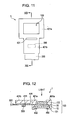
- Fig. 11 is a plan view showing a general configuration of the liquid crystal device according to a third modification in the first embodiment.
- Fig. 12 is a cross-sectional view taken along the line XII-XII in Fig. 11 .
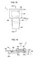
- Fig. 13 is a plan view showing a general configuration of the liquid crystal device according to a fourth modification of the first embodiment.
- Fig. 14 is a cross-sectional view taken along the line XIV-XIV in Fig. 13 .
- Fig. 15 is a plan view showing a general configuration of a liquid crystal device according to a second embodiment.
- Fig. 16 is a cross-sectional view taken along the line XVI-XVI in Fig. 15 .
- Fig. 17 is a plan view showing a configuration of a projector as an example of electronic equipment to which an electro-optic apparatus is applied.
- liquid crystal device of a TFT (Thin Film Transistor) active matrix drive system will be described as an example of an electro-optic apparatus in the invention.
- Fig. 1 to Fig. 6 a first embodiment of the electro-optic apparatus in the invention will be described.
- the scales of the respective layers and members are different from the actual scale throughout the drawings in order to make these layers and members recognizable in the drawings.
- Fig. 1 is a perspective view of the liquid crystal device according to the first embodiment.
- a liquid crystal device 1 includes a liquid crystal panel 100, a wiring board 200 including a plurality of signal lines electrically connected to the liquid crystal panel 100, and a drive IC chip 300 provided on the wiring board 200 and electrically connected to at least part of the plurality of signal lines, and including at least part of a drive circuit for driving the liquid crystal panel 100.
- the drive IC chip 300 includes, for example, part of a data line drive circuit, not shown, and is secured electrically and mechanically to the wiring board 200 using TAB (Tape Automated Bonding) technology.
- the wiring board 200 is formed by patterning the signal lines or the like on a base material formed of polyimide or the like.
- the liquid crystal panel 100 and the drive IC chip 300 correspond to an electro-optic panel and an integrated circuit unit in the invention, respectively.
- the liquid crystal panel 100 is stored in a storage case, which corresponds to an electro-optic apparatus mounting case in the invention, including a frame 401 and a hook 402.
- the frame 401 includes a body portion 401 a for storing the liquid crystal panel 100 and a heat radiating portion 401 b for radiating heat of the drive IC chip 300.
- the heat radiating portion 401 b is formed integrally with the storage case for storing the liquid crystal panel 100.
- the body portion 401 a and the heat radiating portion 401b correspond to the storage case and a heat radiating member in the invention, respectively.
- the frame 401 is formed of metal having high coefficient of thermal conductivity such as aluminum.
- Fig. 2 is a plan view of a TFT array substrate together with respective components formed thereon viewed from a side of an opposed substrate
- Fig. 3 is a cross-sectional view taken along the line III-III in Fig. 2 .
- the liquid crystal panel 100 in the first embodiment includes a TFT array substrate 10 and an opposed substrate 20.
- the TFT array substrate 10 is formed of a transparent substrate such as a quartz substrate, a glass substrate, or a silicon substrate
- the opposed substrate 20 is formed of a transparent substrate such as a quartz substrate or a glass substrate.
- a liquid crystal layer 50 is encapsulated between the TFT array substrate 10 and the opposed substrate 20, and the TFT array substrate 10 and the opposed substrate 20 are bonded to each other by a sealing member 52 provided in a sealing area which is located around an image display area 10a as an example of a "pixel area", which corresponds to an area in which a plurality of pixels are provided.
- the sealing member 52 is formed, for example, of UV-cured resin, heat-cured resin, or UV/heat-cured resin for bonding the two substrates to each other, which is applied on the TFT array substrate 10 in the manufacturing process, and is cured by being irradiated with an ultraviolet ray or by being heated.
- the sealing member 52 contains gap material such as glass fibers or glass beads dispersed therein for adjusting a distance (that is, gap) between the TFT array substrate 10 and the opposed substrate 20 to a predetermined value.
- the gap material may be arranged in the image display area 10a or in a peripheral area around the image display area 10a in addition to, or instead of that mixed in the sealing member 52.
- a frame light-shielding film 53 having a light-shielding property which defines a frame area of the image display area 10a is provided on the side of the opposed substrate 20 in parallel to the inside of the sealing area where the sealing member 52 is arranged.
- part or the entire part of the frame light-shielding film 53 may be provided on the side of the TFT array substrate 10 as an integrated light-shielding film.
- An external circuit connecting terminal 102 is provided in part of the peripheral area located outside the sealing area where the sealing member 52 is arranged along one side of the TFT array substrate 10.
- a sampling circuit 7 is provided inside the sealing area along the one side so as to be covered with the frame light-shielding film 53.
- a scanning line drive circuit 104 is provided inside the sealing areas along two sides adjacent to the one side so as to be covered with the frame light-shielding film 53.
- Upper and lower substrate conducting terminals 106 are provided on the TFT array substrate 10 in areas opposing four corners of the opposed substrate 20 for connecting the two substrates via upper and lower substrate conductors 107. In this arrangement, an electrically conducting state is achieved between the TFT array substrate 10 and the opposed substrate 20.
- a drawn wiring 90 for electrically connecting the external circuit connecting terminal 102, the scanning line drive circuit 104 and the upper and lower substrate conducting terminals 106 is formed on the TFT array substrate 10.
- a laminated structure including wiring such as a pixel switching TFT, scanning lines and data lines as driving elements integrated therein is formed on the TFT array substrate 10.
- pixel electrodes 9a formed of transparent material such as ITO (Indium Tin Oxide) or the like are formed in an island shape in a predetermined pattern on a pixel-to-pixel basis.
- the pixel electrode 9a is formed on the image display area 10a on the TFT array substrate 10 so as to oppose an opposed electrode 21 described later.
- An alignment film 16 is formed on the surface of the TFT array substrate 10 which faces the liquid crystal layer 50, that is, on the pixel electrode 9a, so as to cover the pixel electrode 9a.
- a light-shielding film 23 is formed on the surface of the opposed substrate 20 which opposes the TFT array substrate 10.
- the light-shielding film 23 is formed in a grid-shape in plan view on the opposed surface of the opposed substrate 20.
- non-aperture areas are defined by the light-shielding film 23, and areas partitioned by the light-shielding film 23 correspond to aperture areas which allow transmission of light emitted from a projector lamp or a direct-view backlight. It is also possible to form the light-shielding film 23 in a stripe pattern to define the non-aperture areas by the light-shielding film 23 and respective components such as data lines provided on the side of the TFT array substrate 10.
- the opposed electrodes 21 formed of transparent material such as ITO are formed on the light-shielding film 23 so as to oppose the plurality of pixel electrodes 9a. It is also possible to form a color filter, not shown in Fig. 3 , on the light-shielding film 23 in an area including part of the aperture area and the non-aperture area for performing color display in the image display area 10a.
- An alignment film 22 is formed on the opposed electrodes 21 on an opposed surface of the opposed substrate 20.
- Liquid crystal which constitutes the liquid crystal layer 50 modulates light by the change of alignment and order of an aggregation of molecules depending on the voltage level to be applied and is able to display tones.
- normally white mode the coefficient of transmission with respect to incident light decreases in accordance with the voltage applied on the pixel-to-pixel basis.
- normally black mode the coefficient of transmission with respect to the incident light increases with the voltage applied on the pixel-to-pixel basis. Therefore, light having a contrast according to an image signal is generally emitted from the liquid crystal device.
- a dust-proof substrate 121 and a dust-proof substrate 122 are arranged respectively on a lower layer side of the TFT array substrate 10 and an upper layer side of the opposed substrate 20.
- a pre-charge circuit for supplying pre-charge signals of a predetermined voltage level to a plurality of data lines prior to the image signals and an inspection circuit for inspecting the quality and defects of the liquid crystal device during manufacture or at the time of shipment may be provided in addition to the scanning line drive circuit 104 and the sampling circuit 7.
- a data line drive circuit portion and an image signal supply circuit which correspond to the circuits relating to the supply of the image signals except for the sampling circuit 7 are not formed on the TFT array substrate 10.
- the data line drive circuit portion is integrated exclusively in the drive IC chip 300.
- part of the data line drive circuit portion as such may be provided in the peripheral area between the external circuit connecting terminal 102 and the sealing member 52 on the TFT array substrate 10 (that is, on the side of the sampling circuit 7 via the sealing member 52 along the lower side in Fig. 2 ).
- FIG. 4 is a plan view of the liquid crystal device in the first embodiment viewed from the side of the opposed substrate;
- Fig. 5 is a cross-sectional view taken along the line V-V;
- Fig. 6 is an enlarged cross-sectional view taken along the line VI-VI in Fig. 4 .
- components of the liquid crystal panel 100 shown in fig. 2 and Fig. 3 are omitted as needed for the convenience of description.
- the irregularity of the surface of the heat radiating portion 401 b is exaggerated for the convenience of description.
- the liquid crystal panel 100 is electrically connected to the wiring board 200 via the external circuit connecting terminal 102 (see Fig. 2 ).
- the drive IC chip 300 is secured on the wiring board 200, and the drive IC chip 300 is electrically connected to the liquid crystal panel 100 via at least part of the plurality of signal lines formed on the wiring board 200.
- the liquid crystal panel 100 is driven by the drive IC chip 300, the scanning line drive circuit 104, the sampling circuit 7 or the like (see Fig. 2 ) and a display operation on the image display area 10a (see Fig. 2 ) is achieved.
- the liquid crystal panel 100 is stored in the body portion 401a of the frame 401, and then the hook 402 is mounted.
- the liquid crystal panel 100 and the body portion 401 a are bonded to each other, for example, by a silicon-based mold agent, and the wiring board 200 and the heat radiating portion 401 b are bonded to each other by a bonding portion 411 formed, for example, of a silicon-based mold agent. It is also possible to enhance the coefficient of thermal conductivity by mixing, for example, metal particles in the mold agent.
- the bonding portion 411 may be formed entirely on the portion in which the wiring board 200 and the heat radiating portion 401b are overlapped with each other in plan view.
- Part of heat generated by the drive IC chip 300 is transferred to the heat radiating portion 401b via the wiring board 200 and the bonding portion 411, and is radiated to the air from the heat radiating portion 401b.
- part of heat of the liquid crystal panel 100 is transferred to the body portion 401a, and is radiated to the air from the body portion 401a.
- the body portion 401 a of the frame 401 contributes mainly to radiation of the liquid crystal panel 100
- the heat radiating portion 401b contributes mainly to radiation of the drive IC chip 300.
- the heat radiating portion 401 b has a larger surface area than the drive IC chip 300 as shown in Fig. 4 , and is formed of metal having high coefficient of thermal conductivity, such as aluminum. Therefore, the heat of the drive IC chip 300 is radiated efficiently.
- the surface of the heat radiating portion 401b opposing the wiring board 200 includes fine irregularities. Therefore, if the heat radiating portion 401 b and the wiring board 200 are bonded to each other by double-face adhesive tape or the like, a contact surface of the heat radiating portion 401b is reduced. Therefore, in this embodiment, since the heat radiating portion 401b and the wiring board 200 are bonded to each other by the bonding portion 411 formed, for example, of the silicon-based mold agent, the contact surface of the heat radiating portion 401 b is not reduced. On the contrary, the contact surface between these components may be increased by the mold agent entering the irregular surface, and hence the heat conductivity is further improved. Therefore, the heat of the drive IC chip 300 is efficiently transferred to the heat radiating portion 401 b.
- the heat of the drive IC chip 300 is efficiently radiated, and thermal runaway and thermal rupture of the liquid crystal device 1 are prevented.
- mechanical stress such as bending is applied to the wiring board 200
- the wiring board 200 and the heat radiating portion 401 b are adhered to each other, separation of the drive IC chip 300 from the wiring board 200 is prevented.
- the heat radiating portion 401 b is formed as part of the frame 401, the load applied to the wiring board 200 due to the weight of the heat radiating portion 401 b is reduced.
- FIG. 7 is a plan view of a liquid crystal device according to the first modification when viewed from the side of the opposed substrate, which is similar to Fig. 4
- Fig. 8 is a cross-sectional view taken along the line VIII-VIII in Fig. 7 .
- a radiation fin 421 is arranged on the heat radiating portion 401b.
- the radiation fin 421 and the heat radiating portion 401 b are bonded to each other by the mold agent or the like.
- the radiation fin 421 is formed of metal having a high coefficient of heat conductivity such as aluminum, for example.
- the material to form the radiation fin 421 and the material to from the frame 401 may either be different or the same.
- the surface area which contributes to the radiation is increased, and a good airflow is achieved, so that the heat of the drive IC chip 300 is radiated more efficiently.
- the lateral cross-section of the fin is substantially square in Fig. 7 and Fig. 8 , it may be formed into an oval shape or in a stream line according to the airflow at a position where the electro-optic apparatus is mounted.
- Fig. 9 is a plan view of a liquid crystal device according to the second modification when viewed from the side of the opposite substrate, which is similar to Fig. 4
- Fig. 10 is a cross-sectional view taken along the line X-X in Fig. 9 .
- a radiation fin 422 is formed on the heat radiating portion 401 b.
- the radiation fin 422 is formed integrally with the heat radiating portion 401 b. Accordingly, the heat is easily transferred between the heat radiating portion 401 b and the radiation fin 422.
- the heat radiating portion 401 b and the radiation fin 422 may be manufactured simultaneously, an increase in number of steps in manufacture is prevented.
- Fig. 11 is a plan view of a liquid crystal device according to the third modification when viewed from the side of the opposed substrate, which is similar to Fig. 4
- Fig. 12 is a cross-sectional view taken along the line XII-XII in Fig. 11 .
- the heat radiating portion 401b is formed with an opening 431 along the direction intersecting the direction (vertical direction in Fig. 11 ) in which the plurality of signal lines included in the wiring board 200 extend. (Thus, the opening is formed laterally in Fig. 11 ). Accordingly, the heat is hardly transferred between the heat radiating portion 401 b and the body portion 401 a. Therefore, the drive IC chip 300 is restrained from being affected by the heat of the liquid crystal panel 100 transferred thereto via the frame 401, or the liquid crystal panel 100 is restrained from being affected by the heat of the drive IC chip 300 transferred thereto via the frame 401.
- FIG. 13 is a plan view of a liquid crystal device according to the fourth modification when viewed from the side of the opposed substrate, which is similar to Fig. 4
- Fig. 14 is a cross-sectional view taken along the line XIV-XIV in Fig. 13 .
- the heat radiating portion 401 b is formed with a radiation fin 423 and an opening 432. Accordingly, the heat of the drive IC chip 300 is efficiently radiated, and one of the drive IC chip 300 and the liquid crystal panel 100 is restrained from being affected by the heat transferred from the other.
- Fig. 15 is a plan view of a liquid crystal device according to the second embodiment when viewed from the side of the opposed substrate, which is similar to Fig. 4
- Fig. 16 is a cross-sectional view taken along the line XVI-XVI in Fig. 15 .
- the configuration is the same as the first embodiment except that the heat radiation portion and the drive IC chip are bonded to each other by a bonded part. Therefore, description which is overlapped with the first embodiment is omitted here, and common parts in the drawings are designated by the same reference numerals, and only basically different points are described on the basis of Fig. 15 and Fig. 16 .
- the liquid crystal panel 100 in a liquid crystal device 2 is stored in the body portion 401 a of the frame 401 so that the hook 402 is arranged on the side of the opposed substrate 20 of the liquid crystal panel.
- the drive IC chip 300 and the heat radiating portion 401 b of the frame 401 are bonded to each other by a bonding portion 412 formed of a silicon-based mold agent. Accordingly, the heat of the drive IC chip 300 is efficiently transferred to the heat radiating portion 401b to radiate the heat.
- Fig. 17 a case in which the liquid crystal device described above is applied to a projector which corresponds to electronic equipment will be described.
- the liquid crystal panel 100 in the liquid crystal device described above is used as a light valve of the projector.
- Fig. 17 is a plan view showing a configuration of the projector.
- a lamp unit 1102 formed of a white light source such as a halogen lamp or the like is provided in an interior of a projector 1100.
- a projection light emitted from the lamp unit 1102 is split into three primaries of R, G and B by four mirrors 1106 and two dichroic mirrors 1108 arranged in a light guide 1104 and enters into liquid crystal panels 1110R, 1110B and 1110G as the light valves for the respective primaries.
- the configurations of the liquid crystal panels 1110R, 1110B and 1110G are the same as the liquid crystal device described above, and are driven by primary signals of R, G and B supplied from an image signal processing circuit.
- the light beams modulated by these liquid crystal panels enter a dichroic prism 1112 from three directions.
- the dichroic prism 1112 the light beams of R and B are refracted by 90° and the light beam of G advances straight ahead. Therefore, images of the respective colors are combined, and hence a color image is projected on a screen or the like via a projection lens 1114.
- the images displayed by the liquid crystal panels 1110R and 1110B need to be inverted with respect to the image displayed by the liquid crystal panel 1110G.
- the invention is also applicable to reflective liquid crystal devices (LCOS) formed with elements on a silicon substrate, plasma displays (PDP), field emission displays (FED, SED), organic EL displays, digital micro-mirror devices (DMD), and electrophoresis devices in addition to the liquid crystal devices described in the embodiments shown above.
- LCOS reflective liquid crystal devices
- PDP plasma displays
- FED field emission displays
- SED field emission displays
- organic EL displays organic EL displays
- DMD digital micro-mirror devices
- electrophoresis devices in addition to the liquid crystal devices described in the embodiments shown above.
Landscapes
- Physics & Mathematics (AREA)
- Nonlinear Science (AREA)
- Mathematical Physics (AREA)
- Chemical & Material Sciences (AREA)
- Crystallography & Structural Chemistry (AREA)
- General Physics & Mathematics (AREA)
- Optics & Photonics (AREA)
- Devices For Indicating Variable Information By Combining Individual Elements (AREA)
- Liquid Crystal (AREA)
Abstract
Description
- The present invention relates to an electro-optic apparatus such as a liquid crystal device, an electro-optic apparatus mounting case for mounting the electro-optic apparatus, and electronic equipment such as a liquid crystal projector provided with the electro-optic apparatus and, more specifically, to a technological field relating to a heat radiating member for radiating heat of an integrated circuit provided on a flexible substrate used for the liquid crystal device.
- When the electro-optic apparatus of this type is used as a light valve in electric equipment such as a liquid crystal projector, for example, a strong light source beam from a light source enters an electro-optic panel such as a liquid crystal panel which performs an electro-optical operation such as a display operation in a pixel area of the electro-optic apparatus, for example. Accordingly, the electro-optic panel is likely to rise in temperature, which lowers a performance of the electro-optic panel. Therefore, in order to improve a heat-radiating property of the electro-optic panel, for example, technologies to employ a metal case for storing the electro-optic panel and form a fin on a surface of the case, or to improve coefficient of thermal conductivity by filling adhesive agent into all the clearances formed between the electro-optic panel and the case are proposed (see
JP-A-2003-15104 JP-A-2002-366046 - On the other hand, a technology to provide at least part of a drive circuit for controllably driving the electro-optic panel outside the electro-optic panel as an integrated circuit chip, and connect the electro-optic panel and the integrated circuit chip using a flexible substrate for the purpose of downsizing of the electro-optic panel or widening of the pixel area with respect to the size of the electro-optic panel is also proposed by the applicant of the present application (see
JP-A-2004-252331 - However, in the integrated circuit chip described above, power consumption increases in association with improvement of the throughput, and calorific power due to this operation increases. Therefore, there arises a technological problem such that the electro-optic apparatus is likely to be subjected to thermal runaway or thermal rupture due to the heat generated by the integrated circuit chip. In contrast, according to the technology described in
JP-A-2003-15104 JP-A-2002-366046 - An advantage of some aspects of the invention is that there is provided an electro-optic apparatus which is able to radiate heat generated by an integrated circuit chip efficiently and an electro-optic apparatus mounting case and electronic equipment.
- An electro-optic apparatus according to a first aspect of the invention includes: an electro-optic panel; a wiring board including a plurality of signal lines electrically connected to the electro-optic panel; an integrated circuit unit provided on the wiring board and electrically connected to at least part of the plurality of signal lines; and a heat radiating member arranged so as to overlap at least partly with the integrated circuit unit on the wiring board in plan.
- In this arrangement, the electro-optic apparatus includes the wiring board such as, a flexible substrate or the like for example, including the electro-optic panel such as a liquid crystal panel, the integrated circuit unit including at least part of the drive circuit for driving the electro-optic panel and the plurality of signal lines for electrically connecting the electro-optic panel and the integrated circuit unit. For example, the integrated circuit unit, which is an IC (Integrated Circuit) chip, is electrically and mechanically secured to the wiring board using, for example, TAB (Tape Automated Bonding) technology. When it is operated, the electro-optic panel is driven by the integrated circuit unit or the like, and the electro-optical operation such as a display operation in a pixel area on the electro-optic panel is performed. The term "pixel area" here does not mean individual pixel areas, but means an entire area in which a plurality of pixels are arranged in a plane and, typically, it corresponds to an "image display area" or a "display area".
- The heat radiating member is arranged so as to overlap at least partly with the integrated circuit unit on the wiring board in plan view. The heat radiating member may be arranged on the wiring board on the side where the integrated circuit unit is provided or may be arranged on the wiring board on the opposite side from the side where the integrated circuit unit is provided. When the heat radiating member is arranged on the wiring board on the side where the integrated circuit unit is provided, heat of the integrated circuit unit is transferred to the heat radiating member directly or via adhesive agent or the like which bonds the integrated circuit unit and the heat radiating member to each other. When the heat radiating member is arranged on the wiring board on the opposite side from the side where the integrated circuit unit is provided, the heat of the integrated circuit unit is transferred to the heat radiating member via the wiring board and the adhesive agent or the like which bonds the wiring board and the heat radiating member to each other. Efficiency of heat radiation is improved by forming the heat radiating member of a metal having a high coefficient of thermal conductivity such as copper or aluminum, and the heat of a laminated circuit unit is efficiently radiated.
- According to the study of the inventors of this application, the drive circuit included in the integrated circuit unit is generally becoming complicated and developed by a demand of high definition of display images. In addition, the degree of integration of the integrated circuit unit has been improved by a demand of downsizing of the electro-optic apparatus. Therefore, cooling of the integrated circuit unit is insufficient with a natural convection of air or a forced convection by a fan, and it has turned out that the electro-optic apparatus is likely subjected to thermal runaway or thermal rupture due to the heat generated by the integrated circuit unit.
- Therefore, according to the first aspect of the invention, the heat of the integrated circuit unit is radiated by the heat radiating member arranged so as to be overlapped at least partly with the integrated circuit unit in plan view. By widening a surface area of the heat radiating member as much as possible when the heat radiating member is arranged on the wiring board on the side opposite from the side where the integrated circuit unit is provided, the surface area which contributes to radiate the heat of the integrated circuit is increased. In addition, a bonding surface area is increased, and hence separation of the heat radiating member is prevented. In contrast, in a case in which the heat radiating member is arranged on the wiring board on the side where the integrated circuit unit is provided, for example, by forming the heat radiating member integrally with a storage case for storing the electro-optic panel, an increase in the surface area of the heat radiating member is achieved while reducing a load by the weight of the heat radiating member with respect to the integrated circuit unit.
- Furthermore, when a fin or the like is formed on the heat radiating member, the heat radiating surface area is increased and a good airflow is ensured, whereby the heat of the integrated circuit unit is efficiently radiated. In addition, by bonding the heat radiating member to the integrated circuit unit or the wiring board by the adhesive agent containing metal particles, the heat of the integrated circuit unit is efficiently transferred to the heat radiating member.
- As a result, according to the electro-optic apparatus in the invention, efficient heat radiation of the integrated circuit unit is achieved, and thermal runaway or thermal rupture of the electro-optic apparatus is prevented. Furthermore, in the case in which the heat radiating member is arranged on the wiring board on the opposite side from the side where the integrated circuit unit is provided, the heat radiating member functions also as a lining member. Therefore, electrical disconnection between the integrated circuit unit and the signal lines (more specifically, separation of a terminal unit of an IC chip from the wiring board) in the electro-optic apparatus, caused by mechanical stresses applied from the outside when the electro-optic apparatus is mounted such that the wiring board is bent, is prevented.
- Preferably, a storage case for storing the electro-optic panel is further provided, and the heat radiating member is formed integrally with the storage case.
- In this arrangement, the heat radiating member is typically formed integrally with the storage case so as to extend from the storage case by the same material as the storage case. Therefore, the load due to the weight of the heat radiating member applied to the integrated circuit unit or the wiring board is reduced, and the separation of the heat radiating member is prevented. In addition, since arrangement of the heat radiating member is achieved without increasing the number of steps in manufacture of the electro-optic apparatus, it is very advantageous from a practical standpoint. Furthermore, the heat from the integrated circuit unit is radiated not only into the air but also to the storage case by the heat radiating member. Therefore, radiation of the heat generated at the integrated circuit unit is achieved using a heat radiating function of the storage case. For example, since an air-cooling fan is directed to the storage case and the storage case is provided with the heat-radiating fin, it has a high heat-radiating property. By utilizing a surplus capacity of the heat-radiating property or by enhancing its heat-radiating property, the configuration in the invention is further advantageous.
- Even if the heat radiating member is not formed integrally with the storage case, the same effects are obtained also when the heat radiating member is fixed or mounted mechanically firmly to the storage case and, specifically, when it is fixed or mounted in a manner superior in thermal conductivity, radiation of the heat generated at the integrated circuit unit is achieved using the heat-radiating property of the storage case.
- Preferably, a bonded part which bonds the integrated circuit unit and the heat radiating member to each other is further provided.
- In this arrangement, for example, the bonded part formed, for example, of a silicon-based mold agent bonds the integrated circuit unit and the heat radiating member to each other. Assuming that the integrated circuit unit and the heat radiating member are bonded to each other by double-face adhesive tape or the like, a contact surface is reduced by fine irregularities on the surface of the heat radiating member or the like, so that the heat radiating effect is lowered. Therefore, in the invention, since the bonded part is deformed corresponding to the fine irregularities on the surface of the heat radiating member or the like, reduction in contact surface is prevented. Furthermore, since the heat of the integrated circuit unit is transferred to the heat radiating member only via the bonded part, the heat of the integrated circuit unit is radiated further efficiently.
- Preferably, the wiring board is arranged between the integrated circuit unit and the heat radiating member.
- In this arrangement, the wiring board is arranged between the integrated circuit unit and the heat radiating member. In other words, the heat radiating member is arranged on the wiring board on the opposite side from the side where the integrated circuit unit is provided. In this case, the heat of the integrated circuit unit is transferred to the heat radiating member at least via the wiring board, so that the heat is radiated.
- In this arrangement, specifically, the heat radiating member functions also as the lining member, and hence the electrical disconnection between the integrated circuit unit and the signal lines caused by the mechanical stresses applied from the outside when the electro-optic apparatus is mounted such that the wiring board is bent is prevented, which is vary advantageous from a practical standpoint. When a capacitor or the like is provided on the wiring board, the heat radiating member may be arranged so as to overlap with the integrated circuit unit, the capacitor and the like on the wiring board in plan view. Accordingly, the electrical disconnection between the capacitor and the signal lines is prevented.
- Preferably, a bonded part for bonding the heat radiating member and the wiring board is further provided.
- In this arrangement, the heat radiating member and the wiring board are bonded to each other by the bonded part formed, for example, of the silicon-based mold agent, so that the reduction of the contact surface due to the fine irregularities on the surface of the heat radiating member is prevented.
- Preferably, the heat radiating member includes an opening extending along the direction intersecting the direction of extension of the plurality of signal lines.
- In this arrangement, even though the heat radiating member is formed integrally with the storage case or is firmly fixed or mounted to the storage case, transfer of the heat of the electro-optic panel to the integrated circuit unit via the storage case and the heat radiating member is prevented, or transfer of the heat of the integrated circuit unit to the electro-optic panel is restrained. The opening is typically formed between the electro-optic panel and the integrated circuit unit on the wiring board in plan view. By forming the opening at a position as close to the electro-optic panel as possible, the surface area of the heat radiating member which mainly contributes to the radiation of the heat of the integrated circuit unit is increased. The number of openings is not limited to one, and a plurality of the openings may be formed.
- Preferably, the heat radiating member includes a fin for heat radiation.
- In this arrangement, the heat radiating surface area is increased and good airflow is achieved by the fin, so that the heat of the integrated circuit unit is efficiently radiated. The fin may be provided over the entire surface of the heat radiating member or may be provided in a part. The fin may be formed as a separate member from the heat radiating member, or may be formed integrally with the heat radiating member. When the fin is formed as a separate member, the size or the position of the fin is flexibly changed without reforming the entire storage case according to the electronic equipment provided with the electro-optic apparatus, so that lowering of the flexibility of arrangement in the electronic equipment is avoided, which is very advantageous from a practical standpoint.
- Preferably, the fin is formed integrally with the heat radiating member.
- In this arrangement, the coefficient of thermal conductivity between the heat radiating member and the fin is improved in comparison with the case in which the fin is formed as a separate member. Furthermore, the heat radiating member and the fin may be manufactured in the same step, so that an increase in manufacturing cost is restrained.
- According to a second aspect of the invention, an electro-optic mounting case for storing an electro-optic apparatus including an electro-optic panel; a wiring board including a plurality of signal lines electrically connected to the electro-optic panel; and an integrated circuit unit provided on the wiring board and electrically connected to at least part of the plurality of signal lines, includes a heat radiating member arranged so as to overlap at least partly with the integrated circuit unit on the wiring board in plan view and a storage case for storing the electro-optic panel, and the heat radiating member is formed integrally with the storage case.
- In this arrangement, for example, the electro-optic apparatus mounting case can store the electro-optic apparatus provided with the electro-optic panel such as a liquid crystal panel, the integrated circuit unit including at least part of the drive circuit for driving the electro-optic panel and the wiring board such as a flexible substrate which includes the signal lines for electrically connecting the electro-optic panel and the integrated circuit unit.
- The storage case stores the electro-optic panel. The heat radiating member extends from the storage case along the direction in which the signal lines included in the wiring board extend, and is arranged so as to overlap at least partly with the integrated circuit unit on the wiring board in plan view. By increasing a surface area of the heat radiating member and bonding the heat radiating member and the integrated circuit unit or the wiring board with respect to each other by using a material having high coefficient of thermal conductivity such as a mold agent containing, for example, metal particles, the heat of the integrated circuit unit is efficiently radiated. In addition, since the heat radiating member is formed integrally with the storage case, a load applied to the integrated circuit unit or the wiring board due to the weight of the heat radiating member is reduced, and separation of the heat radiating member is prevented. In addition, since arrangement of the heat radiating member is achieved without increasing the number of steps in manufacture of the electro-optic apparatus, it is very advantageous from a practical standpoint. Furthermore, the heat from the integrated circuit unit is radiated not only into the air but also to the storage case. Therefore, radiation of the heat generated at the integrated circuit unit is achieved using a heat radiating function of the storage case by the heat-radiating member.
- Electronic equipment according to a third aspect of the invention includes the electro-optic apparatus described above (including the various modes thereof).
- According to the electronic equipment in the third aspect of the invention, since the electro-optic apparatus described above is provided, the heat of the integrated circuit unit is efficiently radiated. Therefore, the probability of occurrence of thermal runaway or thermal rupture is reduced, and hence various types of highly reliable electronic equipment such as projecting-type display devices, mobile phones, electronic databooks, word processors, view finder type or direct-view type video tape recorders, workstations, TV-phones, POS terminals, touch panels, and so on are realized.
- Embodiments of the invention will be described by way of example only with reference to the accompanying drawings, wherein like numbers reference like elements.
-
Fig. 1 is a perspective view of a liquid crystal device according to a first embodiment. -
Fig. 2 is a plan view showing a general configuration of a liquid crystal panel according to the first embodiment. -
Fig. 3 is a cross-sectional view taken along the line III-III inFig. 2 . -
Fig. 4 is a plan view showing a general configuration of the liquid crystal device according to the first embodiment. -
Fig. 5 is a cross-sectional view taken along the line V-V inFig. 4 . -
Fig. 6 is a cross-sectional view taken along the line VI-VI inFig. 4 . -
Fig. 7 is a plan view showing a general configuration of the liquid crystal device according to a first modification of the first embodiment. -
Fig. 8 is a cross-sectional view taken along the line VIII-VIII inFig. 7 . -
Fig. 9 is a plan view showing a general configuration of the liquid crystal device according to a second modification of the first embodiment. -
Fig. 10 is a cross-sectional view taken along the line X-X inFig. 9 . -
Fig. 11 is a plan view showing a general configuration of the liquid crystal device according to a third modification in the first embodiment. -
Fig. 12 is a cross-sectional view taken along the line XII-XII inFig. 11 . -
Fig. 13 is a plan view showing a general configuration of the liquid crystal device according to a fourth modification of the first embodiment. -
Fig. 14 is a cross-sectional view taken along the line XIV-XIV inFig. 13 . -
Fig. 15 is a plan view showing a general configuration of a liquid crystal device according to a second embodiment. -
Fig. 16 is a cross-sectional view taken along the line XVI-XVI inFig. 15 . -
Fig. 17 is a plan view showing a configuration of a projector as an example of electronic equipment to which an electro-optic apparatus is applied. - Advantages and other benefits of the invention will be apparent from the description of the exemplary embodiments shown below.
- Referring now to the drawings, embodiments of the invention will be described below. In the embodiments shown below, a liquid crystal device of a TFT (Thin Film Transistor) active matrix drive system will be described as an example of an electro-optic apparatus in the invention.
- Referring now to
Fig. 1 to Fig. 6 , a first embodiment of the electro-optic apparatus in the invention will be described. The scales of the respective layers and members are different from the actual scale throughout the drawings in order to make these layers and members recognizable in the drawings. - First of all, referring now to the drawings, a general configuration of a liquid crystal device in the first embodiment will be described.
Fig. 1 is a perspective view of the liquid crystal device according to the first embodiment. - In
Fig. 1 , aliquid crystal device 1 includes aliquid crystal panel 100, awiring board 200 including a plurality of signal lines electrically connected to theliquid crystal panel 100, and adrive IC chip 300 provided on thewiring board 200 and electrically connected to at least part of the plurality of signal lines, and including at least part of a drive circuit for driving theliquid crystal panel 100. Thedrive IC chip 300 includes, for example, part of a data line drive circuit, not shown, and is secured electrically and mechanically to thewiring board 200 using TAB (Tape Automated Bonding) technology. Thewiring board 200 is formed by patterning the signal lines or the like on a base material formed of polyimide or the like. Theliquid crystal panel 100 and thedrive IC chip 300 correspond to an electro-optic panel and an integrated circuit unit in the invention, respectively. - The
liquid crystal panel 100 is stored in a storage case, which corresponds to an electro-optic apparatus mounting case in the invention, including aframe 401 and ahook 402. Theframe 401 includes abody portion 401 a for storing theliquid crystal panel 100 and aheat radiating portion 401 b for radiating heat of thedrive IC chip 300. In other words, theheat radiating portion 401 b is formed integrally with the storage case for storing theliquid crystal panel 100. Thebody portion 401 a and theheat radiating portion 401b correspond to the storage case and a heat radiating member in the invention, respectively. Theframe 401 is formed of metal having high coefficient of thermal conductivity such as aluminum. - Referring now to
Fig. 2 and Fig. 3 , description of theliquid crystal panel 100 will be added.Fig. 2 is a plan view of a TFT array substrate together with respective components formed thereon viewed from a side of an opposed substrate, andFig. 3 is a cross-sectional view taken along the line III-III inFig. 2 . - In
Fig. 2 and Fig. 3 , theliquid crystal panel 100 in the first embodiment includes aTFT array substrate 10 and anopposed substrate 20. TheTFT array substrate 10 is formed of a transparent substrate such as a quartz substrate, a glass substrate, or a silicon substrate, and theopposed substrate 20 is formed of a transparent substrate such as a quartz substrate or a glass substrate. Aliquid crystal layer 50 is encapsulated between theTFT array substrate 10 and theopposed substrate 20, and theTFT array substrate 10 and theopposed substrate 20 are bonded to each other by a sealingmember 52 provided in a sealing area which is located around animage display area 10a as an example of a "pixel area", which corresponds to an area in which a plurality of pixels are provided. - The sealing
member 52 is formed, for example, of UV-cured resin, heat-cured resin, or UV/heat-cured resin for bonding the two substrates to each other, which is applied on theTFT array substrate 10 in the manufacturing process, and is cured by being irradiated with an ultraviolet ray or by being heated. The sealingmember 52 contains gap material such as glass fibers or glass beads dispersed therein for adjusting a distance (that is, gap) between theTFT array substrate 10 and theopposed substrate 20 to a predetermined value. The gap material may be arranged in theimage display area 10a or in a peripheral area around theimage display area 10a in addition to, or instead of that mixed in the sealingmember 52. - In
Fig. 2 , a frame light-shieldingfilm 53 having a light-shielding property which defines a frame area of theimage display area 10a is provided on the side of the opposedsubstrate 20 in parallel to the inside of the sealing area where the sealingmember 52 is arranged. However, part or the entire part of the frame light-shieldingfilm 53 may be provided on the side of theTFT array substrate 10 as an integrated light-shielding film. - An external
circuit connecting terminal 102 is provided in part of the peripheral area located outside the sealing area where the sealingmember 52 is arranged along one side of theTFT array substrate 10. Asampling circuit 7 is provided inside the sealing area along the one side so as to be covered with the frame light-shieldingfilm 53. A scanningline drive circuit 104 is provided inside the sealing areas along two sides adjacent to the one side so as to be covered with the frame light-shieldingfilm 53. - Upper and lower
substrate conducting terminals 106 are provided on theTFT array substrate 10 in areas opposing four corners of the opposedsubstrate 20 for connecting the two substrates via upper andlower substrate conductors 107. In this arrangement, an electrically conducting state is achieved between theTFT array substrate 10 and theopposed substrate 20. A drawnwiring 90 for electrically connecting the externalcircuit connecting terminal 102, the scanningline drive circuit 104 and the upper and lowersubstrate conducting terminals 106 is formed on theTFT array substrate 10. - In
Fig. 3 , a laminated structure including wiring such as a pixel switching TFT, scanning lines and data lines as driving elements integrated therein is formed on theTFT array substrate 10. Although a detailed configuration of the laminated structure is omitted inFig. 3 ,pixel electrodes 9a formed of transparent material such as ITO (Indium Tin Oxide) or the like are formed in an island shape in a predetermined pattern on a pixel-to-pixel basis. - The
pixel electrode 9a is formed on theimage display area 10a on theTFT array substrate 10 so as to oppose an opposedelectrode 21 described later. Analignment film 16 is formed on the surface of theTFT array substrate 10 which faces theliquid crystal layer 50, that is, on thepixel electrode 9a, so as to cover thepixel electrode 9a. - A light-shielding
film 23 is formed on the surface of the opposedsubstrate 20 which opposes theTFT array substrate 10. The light-shieldingfilm 23 is formed in a grid-shape in plan view on the opposed surface of the opposedsubstrate 20. On the opposedsubstrate 20, non-aperture areas are defined by the light-shieldingfilm 23, and areas partitioned by the light-shieldingfilm 23 correspond to aperture areas which allow transmission of light emitted from a projector lamp or a direct-view backlight. It is also possible to form the light-shieldingfilm 23 in a stripe pattern to define the non-aperture areas by the light-shieldingfilm 23 and respective components such as data lines provided on the side of theTFT array substrate 10. - The
opposed electrodes 21 formed of transparent material such as ITO are formed on the light-shieldingfilm 23 so as to oppose the plurality ofpixel electrodes 9a. It is also possible to form a color filter, not shown inFig. 3 , on the light-shieldingfilm 23 in an area including part of the aperture area and the non-aperture area for performing color display in theimage display area 10a. Analignment film 22 is formed on theopposed electrodes 21 on an opposed surface of the opposedsubstrate 20. - Liquid crystal which constitutes the
liquid crystal layer 50 modulates light by the change of alignment and order of an aggregation of molecules depending on the voltage level to be applied and is able to display tones. In normally white mode, the coefficient of transmission with respect to incident light decreases in accordance with the voltage applied on the pixel-to-pixel basis. In normally black mode, the coefficient of transmission with respect to the incident light increases with the voltage applied on the pixel-to-pixel basis. Therefore, light having a contrast according to an image signal is generally emitted from the liquid crystal device. - As shown in
Fig. 3 , a dust-proof substrate 121 and a dust-proof substrate 122 are arranged respectively on a lower layer side of theTFT array substrate 10 and an upper layer side of the opposedsubstrate 20. - On the
TFT array substrate 10 shown inFig. 2 and Fig. 3 , a pre-charge circuit for supplying pre-charge signals of a predetermined voltage level to a plurality of data lines prior to the image signals and an inspection circuit for inspecting the quality and defects of the liquid crystal device during manufacture or at the time of shipment may be provided in addition to the scanningline drive circuit 104 and thesampling circuit 7. InFig. 2 , a data line drive circuit portion and an image signal supply circuit, which correspond to the circuits relating to the supply of the image signals except for thesampling circuit 7 are not formed on theTFT array substrate 10. In other words, the data line drive circuit portion is integrated exclusively in thedrive IC chip 300. However, part of the data line drive circuit portion as such may be provided in the peripheral area between the externalcircuit connecting terminal 102 and the sealingmember 52 on the TFT array substrate 10 (that is, on the side of thesampling circuit 7 via the sealingmember 52 along the lower side inFig. 2 ). - Referring now to
Fig. 4 to Fig. 6 , the description of theliquid crystal device 1 is addedFig. 4 is a plan view of the liquid crystal device in the first embodiment viewed from the side of the opposed substrate;Fig. 5 is a cross-sectional view taken along the line V-V; andFig. 6 is an enlarged cross-sectional view taken along the line VI-VI inFig. 4 . In these drawings, components of theliquid crystal panel 100 shown infig. 2 and Fig. 3 are omitted as needed for the convenience of description. InFig. 6 , the irregularity of the surface of theheat radiating portion 401 b is exaggerated for the convenience of description. - As shown in
fig. 5 , theliquid crystal panel 100 is electrically connected to thewiring board 200 via the external circuit connecting terminal 102 (seeFig. 2 ). Thedrive IC chip 300 is secured on thewiring board 200, and thedrive IC chip 300 is electrically connected to theliquid crystal panel 100 via at least part of the plurality of signal lines formed on thewiring board 200. Theliquid crystal panel 100 is driven by thedrive IC chip 300, the scanningline drive circuit 104, thesampling circuit 7 or the like (seeFig. 2 ) and a display operation on theimage display area 10a (seeFig. 2 ) is achieved. - When manufacturing the
liquid crystal device 1, theliquid crystal panel 100 is stored in thebody portion 401a of theframe 401, and then thehook 402 is mounted. When storing theliquid crystal panel 100 in thebody portion 401 a, theliquid crystal panel 100 and thebody portion 401 a are bonded to each other, for example, by a silicon-based mold agent, and thewiring board 200 and theheat radiating portion 401 b are bonded to each other by abonding portion 411 formed, for example, of a silicon-based mold agent. It is also possible to enhance the coefficient of thermal conductivity by mixing, for example, metal particles in the mold agent. Thebonding portion 411 may be formed entirely on the portion in which thewiring board 200 and theheat radiating portion 401b are overlapped with each other in plan view. - Part of heat generated by the
drive IC chip 300 is transferred to theheat radiating portion 401b via thewiring board 200 and thebonding portion 411, and is radiated to the air from theheat radiating portion 401b. On the other hand, part of heat of theliquid crystal panel 100 is transferred to thebody portion 401a, and is radiated to the air from thebody portion 401a. In this manner, thebody portion 401 a of theframe 401 contributes mainly to radiation of theliquid crystal panel 100 and theheat radiating portion 401b contributes mainly to radiation of thedrive IC chip 300. In particular, theheat radiating portion 401 b has a larger surface area than thedrive IC chip 300 as shown inFig. 4 , and is formed of metal having high coefficient of thermal conductivity, such as aluminum. Therefore, the heat of thedrive IC chip 300 is radiated efficiently. - As shown in
Fig. 6 , the surface of theheat radiating portion 401b opposing thewiring board 200 includes fine irregularities. Therefore, if theheat radiating portion 401 b and thewiring board 200 are bonded to each other by double-face adhesive tape or the like, a contact surface of theheat radiating portion 401b is reduced. Therefore, in this embodiment, since theheat radiating portion 401b and thewiring board 200 are bonded to each other by thebonding portion 411 formed, for example, of the silicon-based mold agent, the contact surface of theheat radiating portion 401 b is not reduced. On the contrary, the contact surface between these components may be increased by the mold agent entering the irregular surface, and hence the heat conductivity is further improved. Therefore, the heat of thedrive IC chip 300 is efficiently transferred to theheat radiating portion 401 b. - Consequently, according to the
liquid crystal device 1 in the first embodiment, the heat of thedrive IC chip 300 is efficiently radiated, and thermal runaway and thermal rupture of theliquid crystal device 1 are prevented. In addition, even when mechanical stress such as bending is applied to thewiring board 200, since thewiring board 200 and theheat radiating portion 401 b are adhered to each other, separation of thedrive IC chip 300 from thewiring board 200 is prevented. Furthermore, since theheat radiating portion 401 b is formed as part of theframe 401, the load applied to thewiring board 200 due to the weight of theheat radiating portion 401 b is reduced. - Referring now to
Fig. 7 and Fig. 8 , a first modification of the electro-optic apparatus according to the first embodiment will be described.Fig. 7 is a plan view of a liquid crystal device according to the first modification when viewed from the side of the opposed substrate, which is similar toFig. 4 , andFig. 8 is a cross-sectional view taken along the line VIII-VIII inFig. 7 . - As shown in
Fig. 7 and Fig. 8 , aradiation fin 421 is arranged on theheat radiating portion 401b. Typically, theradiation fin 421 and theheat radiating portion 401 b are bonded to each other by the mold agent or the like. Theradiation fin 421 is formed of metal having a high coefficient of heat conductivity such as aluminum, for example. The material to form theradiation fin 421 and the material to from theframe 401 may either be different or the same. - With the provision of the
radiation fin 421, the surface area which contributes to the radiation is increased, and a good airflow is achieved, so that the heat of thedrive IC chip 300 is radiated more efficiently. - Although the lateral cross-section of the fin is substantially square in
Fig. 7 and Fig. 8 , it may be formed into an oval shape or in a stream line according to the airflow at a position where the electro-optic apparatus is mounted. - Referring now to
Fig. 9 and Fig. 10 , a second modification of the electro-optic apparatus according to the first embodiment will be described.Fig. 9 is a plan view of a liquid crystal device according to the second modification when viewed from the side of the opposite substrate, which is similar toFig. 4 , andFig. 10 is a cross-sectional view taken along the line X-X inFig. 9 . - As shown in
Fig. 9 and Fig. 10 , aradiation fin 422 is formed on theheat radiating portion 401 b. In other words, theradiation fin 422 is formed integrally with theheat radiating portion 401 b. Accordingly, the heat is easily transferred between theheat radiating portion 401 b and theradiation fin 422. In addition, since theheat radiating portion 401 b and the radiation fin 422 (and thebody portion 401 a as well) may be manufactured simultaneously, an increase in number of steps in manufacture is prevented. Third Modification - Referring now to
Fig. 11 and Fig. 12 , a third modification of the electro-optic apparatus according to the first embodiment will be described.Fig. 11 is a plan view of a liquid crystal device according to the third modification when viewed from the side of the opposed substrate, which is similar toFig. 4 , andFig. 12 is a cross-sectional view taken along the line XII-XII inFig. 11 . - As shown in
Fig. 11 and Fig. 12 , theheat radiating portion 401b is formed with anopening 431 along the direction intersecting the direction (vertical direction inFig. 11 ) in which the plurality of signal lines included in thewiring board 200 extend. (Thus, the opening is formed laterally inFig. 11 ). Accordingly, the heat is hardly transferred between theheat radiating portion 401 b and thebody portion 401 a. Therefore, thedrive IC chip 300 is restrained from being affected by the heat of theliquid crystal panel 100 transferred thereto via theframe 401, or theliquid crystal panel 100 is restrained from being affected by the heat of thedrive IC chip 300 transferred thereto via theframe 401. - When part of heat radiation by the
heat radiating portion 401 b is carried out by using the heat-radiating property of thebody portion 401 a, the thermal conductivity therebetween may be enhanced by not providing theopening 431. Fourth Modification - Referring now to
Fig. 13 and Fig. 14 , a fourth modification of the electro-optic apparatus according to the first embodiment will be described.Fig. 13 is a plan view of a liquid crystal device according to the fourth modification when viewed from the side of the opposed substrate, which is similar toFig. 4 , andFig. 14 is a cross-sectional view taken along the line XIV-XIV inFig. 13 . - As shown in
Fig. 13 and Fig. 14 , theheat radiating portion 401 b is formed with aradiation fin 423 and anopening 432. Accordingly, the heat of thedrive IC chip 300 is efficiently radiated, and one of thedrive IC chip 300 and theliquid crystal panel 100 is restrained from being affected by the heat transferred from the other. Second Embodiment - Referring now to
Fig. 15 and Fig. 16 , a second embodiment of the electro-optic apparatus in the invention will be described.Fig. 15 is a plan view of a liquid crystal device according to the second embodiment when viewed from the side of the opposed substrate, which is similar toFig. 4 , andFig. 16 is a cross-sectional view taken along the line XVI-XVI inFig. 15 . In the second embodiment, the configuration is the same as the first embodiment except that the heat radiation portion and the drive IC chip are bonded to each other by a bonded part. Therefore, description which is overlapped with the first embodiment is omitted here, and common parts in the drawings are designated by the same reference numerals, and only basically different points are described on the basis ofFig. 15 and Fig. 16 . - As shown in
Fig. 16 , theliquid crystal panel 100 in aliquid crystal device 2 is stored in thebody portion 401 a of theframe 401 so that thehook 402 is arranged on the side of the opposedsubstrate 20 of the liquid crystal panel. For example, thedrive IC chip 300 and theheat radiating portion 401 b of theframe 401 are bonded to each other by abonding portion 412 formed of a silicon-based mold agent. Accordingly, the heat of thedrive IC chip 300 is efficiently transferred to theheat radiating portion 401b to radiate the heat. Electronic Equipment - Referring now to
Fig. 17 , a case in which the liquid crystal device described above is applied to a projector which corresponds to electronic equipment will be described. Theliquid crystal panel 100 in the liquid crystal device described above is used as a light valve of the projector.Fig. 17 is a plan view showing a configuration of the projector. - As shown in
Fig. 17 , alamp unit 1102 formed of a white light source such as a halogen lamp or the like is provided in an interior of aprojector 1100. A projection light emitted from thelamp unit 1102 is split into three primaries of R, G and B by fourmirrors 1106 and twodichroic mirrors 1108 arranged in alight guide 1104 and enters intoliquid crystal panels - The configurations of the
liquid crystal panels dichroic prism 1112 from three directions. In thedichroic prism 1112, the light beams of R and B are refracted by 90° and the light beam of G advances straight ahead. Therefore, images of the respective colors are combined, and hence a color image is projected on a screen or the like via aprojection lens 1114. - When paying attention to the images displayed respectively by the
liquid crystal panels liquid crystal panels liquid crystal panel 1110G. - Since light beams corresponding to the respective primaries R, G and B enter the respective
liquid crystal panels dichroic mirror 1108, it is not necessary to provide a color filter. - In addition to the electronic equipment described on the basis of
Fig. 17 , mobile-type personal computers, mobile phones, liquid crystal TV sets, view finder type or direct-view type video tape recorders, car navigation apparatuses, pagers, electronic databooks, electronic calculators, word processors, workstations, TV phones, POS terminals, and apparatuses having a touch panel are exemplified. Needless to say, the invention is applicable to these types of electronic equipment, among others. - The invention is also applicable to reflective liquid crystal devices (LCOS) formed with elements on a silicon substrate, plasma displays (PDP), field emission displays (FED, SED), organic EL displays, digital micro-mirror devices (DMD), and electrophoresis devices in addition to the liquid crystal devices described in the embodiments shown above.
- The invention is not limited to the embodiments shown above, and may be modified as needed without departing the scope and spirit of the invention understood from the appended claims and the entire specification, and the electro-optic apparatus, the electro-optic apparatus mounting case and the electronic equipment including the electro-optic apparatus associated with these modifications are also included in the technical field of the invention.
Claims (10)
- An electro-optic apparatus comprising:an electro-optic panel (100);a wiring board (200) including a plurality of signal lines electrically connected to the electro-optic panel;an integrated circuit unit (300) provided on the wiring board and electrically connected to at least part of the plurality of signal lines; anda heat radiating member (401b) arranged so as to overlap at least partly with the integrated circuit unit on the wiring board in plan view.
- The electro-optic apparatus according to Claim 1, further comprising: a storage case (401a) for storing the electro-optic panel, wherein the heat radiating member (401b) is formed integrally with the storage case (401a).
- The electro-optic apparatus according to Claim 1 or Claim 2, further comprising: a bonded part (411) which bonds the integrated circuit unit and the heat radiating member to each other.
- The electro-optic apparatus according to any of the preceding claims,
wherein the wiring board is arranged between the integrated circuit unit and the heat radiating member. - The electro-optic apparatus according to Claim 4, further comprising: a bonded part (411) for bonding the heat radiating member and the wiring board.
- The electro-optic apparatus according to any of the preceding claims,
wherein the heat radiating member (401b) includes an opening (431) extending along a direction intersecting a direction of extension of the plurality of signal lines. - The electro-optic apparatus according to any of the preceding claims,
wherein the heat radiating member includes a fin (421, 422) for heat radiation. - The electro-optic apparatus according to Claim 7, wherein the fin is formed integrally with the heat radiating member.
- An electro-optic mounting case (401) for storing an electro-optic apparatus (100) including an electro-optic panel; a wiring board (200) including a plurality of signal lines electrically connected to the electro-optic panel; and an integrated circuit unit (300) provided on the wiring board and electrically connected to at least part of the plurality of signal lines, comprising:a heat radiating member (401b) arranged, when the electro-optic apparatus is stored, so as to overlap at least partly with the integrated circuit unit on the wiring board in plan view; anda storage case (401a) for storing the electro-optic panel,wherein the heat radiating member is formed integrally with the storage case.
- Electronic equipment comprising the electro-optic apparatus according to any one of claims 1 to 8.
Applications Claiming Priority (1)
| Application Number | Priority Date | Filing Date | Title |
|---|---|---|---|
| JP2007245872A JP5504557B2 (en) | 2007-09-21 | 2007-09-21 | Electro-optical device, mounting case for electro-optical device, and electronic apparatus |
Publications (2)
| Publication Number | Publication Date |
|---|---|
| EP2040111A2 true EP2040111A2 (en) | 2009-03-25 |
| EP2040111A3 EP2040111A3 (en) | 2010-03-03 |
Family
ID=40070966
Family Applications (1)
| Application Number | Title | Priority Date | Filing Date |
|---|---|---|---|
| EP08252895A Withdrawn EP2040111A3 (en) | 2007-09-21 | 2008-08-29 | Electro-optic apparatus, electro-optic apparatus mounting case and electronic equipment |
Country Status (6)
| Country | Link |
|---|---|
| US (1) | US7967454B2 (en) |
| EP (1) | EP2040111A3 (en) |
| JP (1) | JP5504557B2 (en) |
| KR (1) | KR101503531B1 (en) |
| CN (1) | CN101393337A (en) |
| TW (1) | TWI470303B (en) |
Families Citing this family (21)
| Publication number | Priority date | Publication date | Assignee | Title |
|---|---|---|---|---|
| JP5034529B2 (en) * | 2007-02-01 | 2012-09-26 | セイコーエプソン株式会社 | Electro-optical device substrate, electro-optical device, and electronic apparatus |
| JP5003366B2 (en) * | 2007-09-10 | 2012-08-15 | セイコーエプソン株式会社 | ELECTRO-OPTICAL DEVICE, MANUFACTURING METHOD THEREOF, AND ELECTRONIC DEVICE |
| JP5245333B2 (en) * | 2007-09-10 | 2013-07-24 | セイコーエプソン株式会社 | Electro-optical device and electronic apparatus |
| JP2009122250A (en) * | 2007-11-13 | 2009-06-04 | Seiko Epson Corp | Electro-optical device and electronic apparatus |
| JP2010181587A (en) * | 2009-02-05 | 2010-08-19 | Sony Corp | Light modulator and projection-type display apparatus |
| JP5533001B2 (en) * | 2010-02-16 | 2014-06-25 | セイコーエプソン株式会社 | Electro-optical device and electronic apparatus |
| JP5672718B2 (en) * | 2010-03-01 | 2015-02-18 | セイコーエプソン株式会社 | Electro-optical device and electronic apparatus |
| JP5423547B2 (en) * | 2010-04-05 | 2014-02-19 | セイコーエプソン株式会社 | Electro-optical device and electronic apparatus |
| JP5445292B2 (en) * | 2010-04-07 | 2014-03-19 | セイコーエプソン株式会社 | Heat dissipation member, electro-optical device, and electronic apparatus |
| JP5724478B2 (en) * | 2011-03-11 | 2015-05-27 | セイコーエプソン株式会社 | Light modulation device and projector |
| JP5741105B2 (en) * | 2011-03-22 | 2015-07-01 | セイコーエプソン株式会社 | Electro-optic device |
| WO2013070833A1 (en) | 2011-11-08 | 2013-05-16 | Taishita LLC | Portable multiuse projector with fiber optic projection |
| JP6015620B2 (en) * | 2013-10-16 | 2016-10-26 | トヨタ自動車株式会社 | vehicle |
| JP6379616B2 (en) * | 2014-04-17 | 2018-08-29 | セイコーエプソン株式会社 | Electro-optical device and electronic apparatus |
| JP6402512B2 (en) * | 2014-07-02 | 2018-10-10 | セイコーエプソン株式会社 | Electro-optic module and electronic equipment |
| KR101570617B1 (en) * | 2014-09-05 | 2015-11-20 | 엘지디스플레이 주식회사 | Flexible printed circuit board and touch panel including the same |
| JP6455154B2 (en) * | 2015-01-08 | 2019-01-23 | 株式会社デンソー | Vehicle electronics |
| JP6507805B2 (en) * | 2015-04-06 | 2019-05-08 | セイコーエプソン株式会社 | Electro-optical module and electronic device |
| CA3036345C (en) * | 2016-09-09 | 2023-12-12 | Photoscience Japan Corporation | Ultraviolet irradiation device and method |
| JP6817862B2 (en) * | 2017-03-24 | 2021-01-20 | 株式会社ジャパンディスプレイ | Display device |
| JP7404690B2 (en) | 2019-07-23 | 2023-12-26 | セイコーエプソン株式会社 | Electro-optical panels, electro-optical devices and electronic equipment |
Citations (4)
| Publication number | Priority date | Publication date | Assignee | Title |
|---|---|---|---|---|
| JP2002366046A (en) | 2001-06-11 | 2002-12-20 | Seiko Epson Corp | Display device and projection device using the same |
| JP2003015104A (en) | 2001-06-29 | 2003-01-15 | Seiko Epson Corp | Display device and projection device using the same |
| JP2004252331A (en) | 2003-02-21 | 2004-09-09 | Seiko Epson Corp | Light modulation device, display device, and electronic device |
| JP2006048019A (en) * | 2004-07-02 | 2006-02-16 | Sony Corp | Liquid crystal display device and liquid crystal projector device |
Family Cites Families (33)
| Publication number | Priority date | Publication date | Assignee | Title |
|---|---|---|---|---|
| DE68924823T2 (en) * | 1988-08-23 | 1996-05-02 | Citizen Watch Co Ltd | Liquid crystal display device. |
| DE69026181D1 (en) * | 1989-10-11 | 1996-05-02 | Sanyo Electric Co | Liquid crystal projector |
| US5146354A (en) * | 1991-05-07 | 1992-09-08 | Compaq Computer Corporation | LCD system with a backlight having a light source at a light pipe's edge and with the LCD enframed |
| CA2071381C (en) * | 1991-07-19 | 1998-12-15 | Youji Satou | Electronic apparatus, card-type electronic component used with the electronic apparatus, and electronic system with expanding apparatus for expanding function of electronic apparatus |
| JPH06194650A (en) * | 1992-12-25 | 1994-07-15 | Citizen Watch Co Ltd | Display device |
| JP3186925B2 (en) * | 1994-08-04 | 2001-07-11 | シャープ株式会社 | Panel mounting structure, integrated circuit mounting tape and method of manufacturing the same |
| JPH0868999A (en) * | 1994-08-31 | 1996-03-12 | Nec Corp | LCD backlight device |
| JPH0943623A (en) * | 1995-08-01 | 1997-02-14 | Denso Corp | Liquid crystal device |
| JPH11305205A (en) * | 1998-04-22 | 1999-11-05 | Hitachi Ltd | Liquid crystal display |
| JP4310039B2 (en) * | 2000-09-29 | 2009-08-05 | エーユー オプトロニクス コーポレイション | IC heat dissipation structure and display device |
| JP3901503B2 (en) * | 2001-07-30 | 2007-04-04 | 株式会社東芝 | Liquid crystal display device and manufacturing method thereof |
| JP3599022B2 (en) * | 2002-01-10 | 2004-12-08 | カシオ計算機株式会社 | Liquid crystal display |
| JP3736523B2 (en) * | 2002-12-20 | 2006-01-18 | セイコーエプソン株式会社 | ELECTRO-OPTICAL DEVICE WITH MOUNTING CASE, PROJECTION TYPE DISPLAY DEVICE, AND MOUNTING CASE |
| JP3908671B2 (en) * | 2003-01-29 | 2007-04-25 | 松下電器産業株式会社 | Semiconductor device and display device using the same |
| EP1445922A1 (en) | 2003-02-06 | 2004-08-11 | Dialog Semiconductor GmbH | Monolithic optical read-out circuit |
| JP3731598B2 (en) * | 2003-03-27 | 2006-01-05 | セイコーエプソン株式会社 | Projection display |
| JP2005077810A (en) | 2003-09-01 | 2005-03-24 | Seiko Epson Corp | Electro-optical device and projection display device |
| JP3923974B2 (en) * | 2003-10-23 | 2007-06-06 | 三星エスディアイ株式会社 | Plasma display device |
| KR100669368B1 (en) * | 2003-10-23 | 2007-01-15 | 삼성에스디아이 주식회사 | Plasma display device with driver IC heat dissipation |
| JP2005310957A (en) | 2004-04-20 | 2005-11-04 | Fujitsu Hitachi Plasma Display Ltd | Display device |
| KR20050122517A (en) * | 2004-06-24 | 2005-12-29 | 삼성에스디아이 주식회사 | Plasma display panel assembly |
| US7365821B2 (en) * | 2004-07-02 | 2008-04-29 | Sony Corporation | Liquid crystal display having dummy bump connected to dummy lead for heat reduction |
| JP2006064939A (en) * | 2004-08-26 | 2006-03-09 | Optrex Corp | Display device |
| US7625091B2 (en) * | 2004-09-06 | 2009-12-01 | Nikon Corporation | Illuminating device and projector device |
| JP4622430B2 (en) * | 2004-09-30 | 2011-02-02 | セイコーエプソン株式会社 | Liquid crystal display device |
| JP4251129B2 (en) * | 2004-10-25 | 2009-04-08 | セイコーエプソン株式会社 | Mounting structure, electro-optical device, and electronic apparatus |
| KR100669756B1 (en) * | 2004-11-11 | 2007-01-16 | 삼성에스디아이 주식회사 | Plasma display assembly |
| JP2006171299A (en) * | 2004-12-15 | 2006-06-29 | Sony Corp | Liquid crystal display device and shading device |
| JP2006301256A (en) * | 2005-04-20 | 2006-11-02 | Sony Corp | Device and electronic apparatus using circuit board |
| KR20060126070A (en) * | 2005-06-03 | 2006-12-07 | 삼성전자주식회사 | Drive integrated circuit chip package and display device having same |
| KR101138261B1 (en) * | 2005-06-29 | 2012-04-24 | 엘지디스플레이 주식회사 | liquid crystal display device |
| JP4237748B2 (en) * | 2005-12-09 | 2009-03-11 | カシオ計算機株式会社 | Display module |
| US7808573B2 (en) * | 2008-08-14 | 2010-10-05 | Himax Display, Inc. | Display (LCOS) panel module having an adhesive on a subtrate with a flexible printed circuit (FPC) having an opening so that the LCOS panel may be adhesively connected to the substrate and electrically connected to the FPC through the opening |
-
2007
- 2007-09-21 JP JP2007245872A patent/JP5504557B2/en active Active
-
2008
- 2008-08-29 EP EP08252895A patent/EP2040111A3/en not_active Withdrawn
- 2008-09-12 KR KR1020080090245A patent/KR101503531B1/en active Active
- 2008-09-19 US US12/233,984 patent/US7967454B2/en active Active
- 2008-09-19 TW TW97136131A patent/TWI470303B/en active
- 2008-09-19 CN CNA2008101491749A patent/CN101393337A/en active Pending
Patent Citations (4)
| Publication number | Priority date | Publication date | Assignee | Title |
|---|---|---|---|---|
| JP2002366046A (en) | 2001-06-11 | 2002-12-20 | Seiko Epson Corp | Display device and projection device using the same |
| JP2003015104A (en) | 2001-06-29 | 2003-01-15 | Seiko Epson Corp | Display device and projection device using the same |
| JP2004252331A (en) | 2003-02-21 | 2004-09-09 | Seiko Epson Corp | Light modulation device, display device, and electronic device |
| JP2006048019A (en) * | 2004-07-02 | 2006-02-16 | Sony Corp | Liquid crystal display device and liquid crystal projector device |
Also Published As
| Publication number | Publication date |
|---|---|
| KR20090031242A (en) | 2009-03-25 |
| JP5504557B2 (en) | 2014-05-28 |
| JP2009075457A (en) | 2009-04-09 |
| TW200931107A (en) | 2009-07-16 |
| US20090080154A1 (en) | 2009-03-26 |
| KR101503531B1 (en) | 2015-03-17 |
| TWI470303B (en) | 2015-01-21 |
| EP2040111A3 (en) | 2010-03-03 |
| CN101393337A (en) | 2009-03-25 |
| US7967454B2 (en) | 2011-06-28 |
Similar Documents
| Publication | Publication Date | Title |
|---|---|---|
| US7967454B2 (en) | Electro-optic apparatus and electronic equipment | |
| US8988883B2 (en) | Electro-optic device and electronic device | |
| JP5453762B2 (en) | Electro-optical device and electronic apparatus | |
| JP2009075503A (en) | Electro-optical device and electronic apparatus including the same | |
| US11204623B2 (en) | Electro-optical device and electronic apparatus | |
| JP5109713B2 (en) | Electro-optical device and electronic apparatus | |
| JP2010256666A (en) | Electro-optical device and electronic apparatus | |
| JP2009204958A (en) | Electro-optic device and method for manufacturing the same, and electronic apparatus | |
| JP5500217B2 (en) | Electro-optical device and electronic apparatus | |
| CN101266344B (en) | Heat dispersion component, electro-optical device and electronic apparatus | |
| JP5169153B2 (en) | Electro-optical device and electronic apparatus | |
| JP5115153B2 (en) | Electro-optical device and electronic apparatus | |
| JP4747572B2 (en) | Electro-optical device and electronic apparatus | |
| JP2010256662A (en) | Electro-optical device and electronic apparatus | |
| JP5109705B2 (en) | Electro-optical device and electronic apparatus | |
| JP2010256663A (en) | Electro-optical device and electronic apparatus | |
| JP5104156B2 (en) | ELECTRO-OPTICAL DEVICE AND ELECTRONIC DEVICE HAVING THE SAME | |
| JP2009122309A (en) | Electro-optical device manufacturing method, electro-optical device, and electronic apparatus | |
| JP2009128665A (en) | Electro-optical device and electronic apparatus | |
| US9116381B2 (en) | Electro-optical device and electronic apparatus | |
| JP2009198542A (en) | Electrooptical apparatus and electronic equipment | |
| JP2010175818A (en) | Electro-optical apparatus and electronic device | |
| JP2010060968A (en) | Electro-optical device and electronic apparatus | |
| JP2010091877A (en) | Electro-optical device and electronic equipment | |
| JP2011145445A (en) | Electro-optical device and electronic apparatus |
Legal Events
| Date | Code | Title | Description |
|---|---|---|---|
| PUAI | Public reference made under article 153(3) epc to a published international application that has entered the european phase |
Free format text: ORIGINAL CODE: 0009012 |
|
| AK | Designated contracting states |
Kind code of ref document: A2 Designated state(s): AT BE BG CH CY CZ DE DK EE ES FI FR GB GR HR HU IE IS IT LI LT LU LV MC MT NL NO PL PT RO SE SI SK TR |
|
| AX | Request for extension of the european patent |
Extension state: AL BA MK RS |
|
| PUAL | Search report despatched |
Free format text: ORIGINAL CODE: 0009013 |
|
| AK | Designated contracting states |
Kind code of ref document: A3 Designated state(s): AT BE BG CH CY CZ DE DK EE ES FI FR GB GR HR HU IE IS IT LI LT LU LV MC MT NL NO PL PT RO SE SI SK TR |
|
| AX | Request for extension of the european patent |
Extension state: AL BA MK RS |
|
| RIC1 | Information provided on ipc code assigned before grant |
Ipc: G02F 1/133 20060101ALI20100122BHEP Ipc: H05K 7/20 20060101ALI20100122BHEP Ipc: G02F 1/13 20060101AFI20081209BHEP |
|
| 17P | Request for examination filed |
Effective date: 20100903 |
|
| AKX | Designation fees paid |
Designated state(s): DE FR GB |
|
| 17Q | First examination report despatched |
Effective date: 20140324 |
|
| STAA | Information on the status of an ep patent application or granted ep patent |
Free format text: STATUS: THE APPLICATION IS DEEMED TO BE WITHDRAWN |
|
| 18D | Application deemed to be withdrawn |
Effective date: 20170815 |