EP2037493A2 - Method of mounting conductive ball and conductive ball mounting apparatus - Google Patents
Method of mounting conductive ball and conductive ball mounting apparatus Download PDFInfo
- Publication number
- EP2037493A2 EP2037493A2 EP08161922A EP08161922A EP2037493A2 EP 2037493 A2 EP2037493 A2 EP 2037493A2 EP 08161922 A EP08161922 A EP 08161922A EP 08161922 A EP08161922 A EP 08161922A EP 2037493 A2 EP2037493 A2 EP 2037493A2
- Authority
- EP
- European Patent Office
- Prior art keywords
- mask
- ball
- conductive
- conductive balls
- mounting
- Prior art date
- Legal status (The legal status is an assumption and is not a legal conclusion. Google has not performed a legal analysis and makes no representation as to the accuracy of the status listed.)
- Granted
Links
- 238000000034 method Methods 0.000 title claims abstract description 53
- 239000000758 substrate Substances 0.000 claims abstract description 95
- 239000002313 adhesive film Substances 0.000 claims abstract description 43
- 239000004065 semiconductor Substances 0.000 claims description 27
- 238000001179 sorption measurement Methods 0.000 claims description 5
- 229910000679 solder Inorganic materials 0.000 description 49
- 239000010410 layer Substances 0.000 description 18
- 230000004907 flux Effects 0.000 description 8
- 238000004519 manufacturing process Methods 0.000 description 5
- 239000002184 metal Substances 0.000 description 5
- 229910052751 metal Inorganic materials 0.000 description 5
- 239000011229 interlayer Substances 0.000 description 4
- RYGMFSIKBFXOCR-UHFFFAOYSA-N Copper Chemical compound [Cu] RYGMFSIKBFXOCR-UHFFFAOYSA-N 0.000 description 3
- 238000007664 blowing Methods 0.000 description 3
- 229910052802 copper Inorganic materials 0.000 description 3
- 239000010949 copper Substances 0.000 description 3
- 229920005989 resin Polymers 0.000 description 3
- 239000011347 resin Substances 0.000 description 3
- XUIMIQQOPSSXEZ-UHFFFAOYSA-N Silicon Chemical compound [Si] XUIMIQQOPSSXEZ-UHFFFAOYSA-N 0.000 description 2
- 229910052710 silicon Inorganic materials 0.000 description 2
- 239000010703 silicon Substances 0.000 description 2
- 239000004593 Epoxy Substances 0.000 description 1
- 239000004642 Polyimide Substances 0.000 description 1
- 239000004020 conductor Substances 0.000 description 1
- 230000000694 effects Effects 0.000 description 1
- 230000005611 electricity Effects 0.000 description 1
- 239000003822 epoxy resin Substances 0.000 description 1
- 239000011521 glass Substances 0.000 description 1
- 238000010438 heat treatment Methods 0.000 description 1
- 238000012423 maintenance Methods 0.000 description 1
- 238000005192 partition Methods 0.000 description 1
- 229920000647 polyepoxide Polymers 0.000 description 1
- 229920001721 polyimide Polymers 0.000 description 1
- 125000006850 spacer group Chemical group 0.000 description 1
- 230000003068 static effect Effects 0.000 description 1
- 238000010408 sweeping Methods 0.000 description 1
Images


Classifications
-
- H—ELECTRICITY
- H01—ELECTRIC ELEMENTS
- H01L—SEMICONDUCTOR DEVICES NOT COVERED BY CLASS H10
- H01L21/00—Processes or apparatus adapted for the manufacture or treatment of semiconductor or solid state devices or of parts thereof
- H01L21/02—Manufacture or treatment of semiconductor devices or of parts thereof
- H01L21/04—Manufacture or treatment of semiconductor devices or of parts thereof the devices having potential barriers, e.g. a PN junction, depletion layer or carrier concentration layer
- H01L21/48—Manufacture or treatment of parts, e.g. containers, prior to assembly of the devices, using processes not provided for in a single one of the subgroups H01L21/06 - H01L21/326
- H01L21/4814—Conductive parts
- H01L21/4846—Leads on or in insulating or insulated substrates, e.g. metallisation
- H01L21/4853—Connection or disconnection of other leads to or from a metallisation, e.g. pins, wires, bumps
-
- B—PERFORMING OPERATIONS; TRANSPORTING
- B23—MACHINE TOOLS; METAL-WORKING NOT OTHERWISE PROVIDED FOR
- B23K—SOLDERING OR UNSOLDERING; WELDING; CLADDING OR PLATING BY SOLDERING OR WELDING; CUTTING BY APPLYING HEAT LOCALLY, e.g. FLAME CUTTING; WORKING BY LASER BEAM
- B23K3/00—Tools, devices, or special appurtenances for soldering, e.g. brazing, or unsoldering, not specially adapted for particular methods
- B23K3/06—Solder feeding devices; Solder melting pans
- B23K3/0607—Solder feeding devices
- B23K3/0623—Solder feeding devices for shaped solder piece feeding, e.g. preforms, bumps, balls, pellets, droplets
-
- H—ELECTRICITY
- H01—ELECTRIC ELEMENTS
- H01L—SEMICONDUCTOR DEVICES NOT COVERED BY CLASS H10
- H01L24/00—Arrangements for connecting or disconnecting semiconductor or solid-state bodies; Methods or apparatus related thereto
- H01L24/74—Apparatus for manufacturing arrangements for connecting or disconnecting semiconductor or solid-state bodies
- H01L24/741—Apparatus for manufacturing means for bonding, e.g. connectors
- H01L24/742—Apparatus for manufacturing bump connectors
-
- H—ELECTRICITY
- H05—ELECTRIC TECHNIQUES NOT OTHERWISE PROVIDED FOR
- H05K—PRINTED CIRCUITS; CASINGS OR CONSTRUCTIONAL DETAILS OF ELECTRIC APPARATUS; MANUFACTURE OF ASSEMBLAGES OF ELECTRICAL COMPONENTS
- H05K3/00—Apparatus or processes for manufacturing printed circuits
- H05K3/30—Assembling printed circuits with electric components, e.g. with resistor
- H05K3/32—Assembling printed circuits with electric components, e.g. with resistor electrically connecting electric components or wires to printed circuits
- H05K3/34—Assembling printed circuits with electric components, e.g. with resistor electrically connecting electric components or wires to printed circuits by soldering
- H05K3/3457—Solder materials or compositions; Methods of application thereof
- H05K3/3478—Applying solder preforms; Transferring prefabricated solder patterns
-
- B—PERFORMING OPERATIONS; TRANSPORTING
- B23—MACHINE TOOLS; METAL-WORKING NOT OTHERWISE PROVIDED FOR
- B23K—SOLDERING OR UNSOLDERING; WELDING; CLADDING OR PLATING BY SOLDERING OR WELDING; CUTTING BY APPLYING HEAT LOCALLY, e.g. FLAME CUTTING; WORKING BY LASER BEAM
- B23K2101/00—Articles made by soldering, welding or cutting
- B23K2101/36—Electric or electronic devices
- B23K2101/40—Semiconductor devices
-
- H—ELECTRICITY
- H01—ELECTRIC ELEMENTS
- H01L—SEMICONDUCTOR DEVICES NOT COVERED BY CLASS H10
- H01L2224/00—Indexing scheme for arrangements for connecting or disconnecting semiconductor or solid-state bodies and methods related thereto as covered by H01L24/00
- H01L2224/01—Means for bonding being attached to, or being formed on, the surface to be connected, e.g. chip-to-package, die-attach, "first-level" interconnects; Manufacturing methods related thereto
- H01L2224/10—Bump connectors; Manufacturing methods related thereto
- H01L2224/11—Manufacturing methods
- H01L2224/11001—Involving a temporary auxiliary member not forming part of the manufacturing apparatus, e.g. removable or sacrificial coating, film or substrate
- H01L2224/11003—Involving a temporary auxiliary member not forming part of the manufacturing apparatus, e.g. removable or sacrificial coating, film or substrate for holding or transferring the bump preform
-
- H—ELECTRICITY
- H01—ELECTRIC ELEMENTS
- H01L—SEMICONDUCTOR DEVICES NOT COVERED BY CLASS H10
- H01L2224/00—Indexing scheme for arrangements for connecting or disconnecting semiconductor or solid-state bodies and methods related thereto as covered by H01L24/00
- H01L2224/01—Means for bonding being attached to, or being formed on, the surface to be connected, e.g. chip-to-package, die-attach, "first-level" interconnects; Manufacturing methods related thereto
- H01L2224/10—Bump connectors; Manufacturing methods related thereto
- H01L2224/11—Manufacturing methods
- H01L2224/11001—Involving a temporary auxiliary member not forming part of the manufacturing apparatus, e.g. removable or sacrificial coating, film or substrate
- H01L2224/11005—Involving a temporary auxiliary member not forming part of the manufacturing apparatus, e.g. removable or sacrificial coating, film or substrate for aligning the bump connector, e.g. marks, spacers
-
- H—ELECTRICITY
- H01—ELECTRIC ELEMENTS
- H01L—SEMICONDUCTOR DEVICES NOT COVERED BY CLASS H10
- H01L2224/00—Indexing scheme for arrangements for connecting or disconnecting semiconductor or solid-state bodies and methods related thereto as covered by H01L24/00
- H01L2224/01—Means for bonding being attached to, or being formed on, the surface to be connected, e.g. chip-to-package, die-attach, "first-level" interconnects; Manufacturing methods related thereto
- H01L2224/10—Bump connectors; Manufacturing methods related thereto
- H01L2224/11—Manufacturing methods
- H01L2224/113—Manufacturing methods by local deposition of the material of the bump connector
- H01L2224/1133—Manufacturing methods by local deposition of the material of the bump connector in solid form
- H01L2224/11334—Manufacturing methods by local deposition of the material of the bump connector in solid form using preformed bumps
-
- H—ELECTRICITY
- H01—ELECTRIC ELEMENTS
- H01L—SEMICONDUCTOR DEVICES NOT COVERED BY CLASS H10
- H01L2224/00—Indexing scheme for arrangements for connecting or disconnecting semiconductor or solid-state bodies and methods related thereto as covered by H01L24/00
- H01L2224/01—Means for bonding being attached to, or being formed on, the surface to be connected, e.g. chip-to-package, die-attach, "first-level" interconnects; Manufacturing methods related thereto
- H01L2224/10—Bump connectors; Manufacturing methods related thereto
- H01L2224/15—Structure, shape, material or disposition of the bump connectors after the connecting process
- H01L2224/16—Structure, shape, material or disposition of the bump connectors after the connecting process of an individual bump connector
- H01L2224/161—Disposition
- H01L2224/16151—Disposition the bump connector connecting between a semiconductor or solid-state body and an item not being a semiconductor or solid-state body, e.g. chip-to-substrate, chip-to-passive
- H01L2224/16221—Disposition the bump connector connecting between a semiconductor or solid-state body and an item not being a semiconductor or solid-state body, e.g. chip-to-substrate, chip-to-passive the body and the item being stacked
- H01L2224/16225—Disposition the bump connector connecting between a semiconductor or solid-state body and an item not being a semiconductor or solid-state body, e.g. chip-to-substrate, chip-to-passive the body and the item being stacked the item being non-metallic, e.g. insulating substrate with or without metallisation
-
- H—ELECTRICITY
- H01—ELECTRIC ELEMENTS
- H01L—SEMICONDUCTOR DEVICES NOT COVERED BY CLASS H10
- H01L2924/00—Indexing scheme for arrangements or methods for connecting or disconnecting semiconductor or solid-state bodies as covered by H01L24/00
- H01L2924/01—Chemical elements
- H01L2924/01005—Boron [B]
-
- H—ELECTRICITY
- H01—ELECTRIC ELEMENTS
- H01L—SEMICONDUCTOR DEVICES NOT COVERED BY CLASS H10
- H01L2924/00—Indexing scheme for arrangements or methods for connecting or disconnecting semiconductor or solid-state bodies as covered by H01L24/00
- H01L2924/01—Chemical elements
- H01L2924/01006—Carbon [C]
-
- H—ELECTRICITY
- H01—ELECTRIC ELEMENTS
- H01L—SEMICONDUCTOR DEVICES NOT COVERED BY CLASS H10
- H01L2924/00—Indexing scheme for arrangements or methods for connecting or disconnecting semiconductor or solid-state bodies as covered by H01L24/00
- H01L2924/01—Chemical elements
- H01L2924/01029—Copper [Cu]
-
- H—ELECTRICITY
- H05—ELECTRIC TECHNIQUES NOT OTHERWISE PROVIDED FOR
- H05K—PRINTED CIRCUITS; CASINGS OR CONSTRUCTIONAL DETAILS OF ELECTRIC APPARATUS; MANUFACTURE OF ASSEMBLAGES OF ELECTRICAL COMPONENTS
- H05K2203/00—Indexing scheme relating to apparatus or processes for manufacturing printed circuits covered by H05K3/00
- H05K2203/01—Tools for processing; Objects used during processing
- H05K2203/0104—Tools for processing; Objects used during processing for patterning or coating
- H05K2203/0139—Blade or squeegee, e.g. for screen printing or filling of holes
-
- H—ELECTRICITY
- H05—ELECTRIC TECHNIQUES NOT OTHERWISE PROVIDED FOR
- H05K—PRINTED CIRCUITS; CASINGS OR CONSTRUCTIONAL DETAILS OF ELECTRIC APPARATUS; MANUFACTURE OF ASSEMBLAGES OF ELECTRICAL COMPONENTS
- H05K2203/00—Indexing scheme relating to apparatus or processes for manufacturing printed circuits covered by H05K3/00
- H05K2203/01—Tools for processing; Objects used during processing
- H05K2203/0191—Using tape or non-metallic foil in a process, e.g. during filling of a hole with conductive paste
-
- H—ELECTRICITY
- H05—ELECTRIC TECHNIQUES NOT OTHERWISE PROVIDED FOR
- H05K—PRINTED CIRCUITS; CASINGS OR CONSTRUCTIONAL DETAILS OF ELECTRIC APPARATUS; MANUFACTURE OF ASSEMBLAGES OF ELECTRICAL COMPONENTS
- H05K2203/00—Indexing scheme relating to apparatus or processes for manufacturing printed circuits covered by H05K3/00
- H05K2203/04—Soldering or other types of metallurgic bonding
- H05K2203/041—Solder preforms in the shape of solder balls
-
- H—ELECTRICITY
- H05—ELECTRIC TECHNIQUES NOT OTHERWISE PROVIDED FOR
- H05K—PRINTED CIRCUITS; CASINGS OR CONSTRUCTIONAL DETAILS OF ELECTRIC APPARATUS; MANUFACTURE OF ASSEMBLAGES OF ELECTRICAL COMPONENTS
- H05K2203/00—Indexing scheme relating to apparatus or processes for manufacturing printed circuits covered by H05K3/00
- H05K2203/05—Patterning and lithography; Masks; Details of resist
- H05K2203/0548—Masks
- H05K2203/0557—Non-printed masks
Definitions
- the present invention relates to a method of mounting a conductive ball and a conductive ball mounting apparatus, more particularly, a method of mounting a conductive ball and a conductive ball mounting apparatus, for mounting a conductive ball on a wiring substrate or the like to form a bump electrode.
- a method of forming a solder ball on a connection pad of a wiring substrate on which a semiconductor chip or the like is to be mounted, and thereby forming a bump electrode In such a method of mounting a solder ball, firstly, as shown in FIG. 1A , a wiring substrate 100 on which solder balls are to be mounted is prepared. In the wiring substrate 100, connection pads 200 are provided on an upper surface of a substrate 110, and a solder resist 300 in which opening portions 300a are provided on the connection pads 200 is formed. Moreover, a flux 400 is coated on the connection pads 200.
- a mask 500 to be used for mounting solder balls is disposed on the wiring substrate 100.
- the mask 500 has a configuration in which a mesh portion 540 is attached to a periphery of a metal mask portion 520, and in which a frame portion 560 is provided on the outer edge of the mesh portion 540. Moreover, opening portions 500a through which solder balls pass are formed in parts of the mask portion 520, the parts corresponding to the connection pads 200 of the wiring substrate 100.
- solder balls 600 are supplied onto the mask 500 and then swept to move to one end side of the mask 500 by a brush 700.
- the solder balls 600 pass through the opening portions 500a of the mask 500 and are arranged to be bonded to the fluxes 400 on the connection pads 200 of the wiring substrate 100.
- the mask 500 is moved upward to be removed from the wiring substrate 100.
- FIG. 2 there is another method using an air supply 750 instead of the use of the brush 700.
- this method by blowing air to the solder balls 600 from an air supply 750 to move the solder balls 600 to one end side of the mask 500, the solder balls 600 is arranged on the connection pads 200 of the wiring substrate 100 while causing the solder balls 600 to pass through the opening portions 500a of the mask 500.
- Patent Literature 1 Japanese Patent Application Publication No. 2004-186286
- a print mask is disposed on a silicon substrate having columnar electrodes, then a large number of solder balls are supplied on the print mask, then air is moderately blown to the solder balls while a squeegee is moved, thereby, solder balls pass through the print mask, and are arranged on the columnar electrodes.
- Patent Literature 2 Japanese Patent Application Publication No. 2006-173195
- a large number of solder balls are supplied on a mask disposed on a wafer, then the solder balls are moved by a filling head provided with a sweep member, to arrange the solder balls in opening portions in the mask, then the solder balls remaining on the mask are swept to the outside of the mask by a removal head provided with a soft squeegee, and are removed consequently.
- solder balls 600 the number of which is considerably larger than that of the opening portions 500a of the mask 500 are supplied on the mask 500. Accordingly, although some of the solder balls 600 pass through the opening portions 500a of the mask 500, some other solder balls 600 remain around the opening portions 500a of the mask 500 in many cases. Such being the case, it is necessary to move the excess solder balls 600 to one end side of the mask 500, or to remove the excess solder balls 600 from the mask 500.
- the excess solder balls 600 remaining on the mask 500 may pass through the opening portions 500a of the mask 500 when the mask 500 is moved upward from the wiring substrate 100 to be separated therefrom, and consequently, multiple solder balls are likely to be mounted on the connection pads 200 of the wiring substrate 100, in some cases.
- the brush In the method in which the excess solder balls on the mask are moved by the brush, the brush needs to be moved repeatedly with many times in order to remove all the excess solder balls. Consequently, a long time is required for the operation, and, hence, the manufacturing efficiency is low. Furthermore, solder balls sometimes adhere to the brush, which is likely to complicate the maintenance.
- the wind pressure needs to be set relatively high in order to efficiently move the solder balls.
- solder balls on the mask sometimes fly to the outside of the mask in some cases.
- the wind pressure is set low enough to prevent solder balls from flying to the outside, it is extremely difficult to move all the excess solder balls.
- a method of mounting a conductive ball which method includes the steps of: disposing a mask on a substrate including connection pads, the mask having opening portions corresponding to the connection pads; supplying conductive balls on the mask; arranging the conductive balls on the connection pad of the substrate through the opening portion of the mask, by moving the conductive balls to one end side of the mask by a ball moving member; and removing excess conductive balls remaining on a region of the mask where the opening portions are provided, by bonding the excess conductive balls to a ball removal film.
- a mask is disposed on a substrate (such as a wiring substrate, or a semiconductor wafer in which semiconductor element is made) having connection pads, the mask having opening portions corresponding to the connection pads. Thereafter, a larger number of conductive balls (solder balls or the like) than that of the opening portions are supplied on the mask.
- the conductive balls are swept and moved to one end side of the mask by moving ball moving member (a brush or the like) in a horizontal direction. Thereby, the conductive balls pass through the opening portions of the mask, and are arranged respectively on the connection pads of the substrate. At this stage, some of the conductive balls remain as excess in regions in which the opening portions are formed, on the mask.
- moving ball moving member a brush or the like
- the excess conductive balls on the mask are bonded to a ball removing film (such as an adhesive film or an electrostatic adsorption film), thereby the excess conductive balls are removed from the mask consequently.
- a ball removing film such as an adhesive film or an electrostatic adsorption film
- this method prevents the excess conductive balls from being mounted on the substrate through the opening portions of the mask when the mask is moved upward to be removed from the substrate. Accordingly, a single conductive ball can be mounted on each of the connection pads of the substrate with high reliability.
- the ball removal film is placed in parallel with the mask in a state that a roll-like film is pulled out. After the conductive balls adhere to the ball removal film and are then removed, a used part of the film is wound, and a new part of the ball removal film is placed on the mask.
- a protrusion portion protruding upward may be provided on an upper surface of the mask. According to this embodiment, even when the ball removal film is displaced closer to the mask, the protrusion portion serves as a stopper, so that the height position of the ball removal film is controlled to be a desired position. Thus, only the excess conductive balls on the mask are selectively removed in a stable manner without removing the conductive balls passing through the opening portions of the mask.
- conductive balls can be mounted on a substrate with high reliability while excess conductive balls on the mask are removed efficiently.
- FIGS. 3 to 9 are cross-sectional views showing a method of mounting a conductive ball, according to a first embodiment of the present invention
- FIGS. 10 to 12 are cross-sectional views showing a method of mounting a semiconductor chip on a wiring substrate on which conductive balls are mounted
- FIG. 13 is a cross-sectional view showing a conductive ball mounting apparatus similarly.
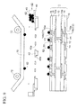
- a wiring substrate 1 on which conductive balls are to be mounted is prepared.
- through holes TH are formed in a core substrate 10 made of glass epoxy resin or the like, and the through holes TH are filled respectively with through-hole electrodes 12 made of copper or the like.
- first wiring layers 14a connected to each other via through-hole electrode 12 and made of copper, are respectively formed on both surfaces of the core substrate 10.
- the first wiring layers 14a which are formed on the both surfaces of the core substrate 10 may be connected to each other with a through-hole plated layer formed on an inner wall of the through holes TH, and the opening in the through holes TH may be filled with resin.
- interlayer insulating films 16 for covering the first wiring layers 14a are formed respectively.
- the interlayer insulating films 16 are formed by affixing resin films made of epoxy, polyimide or the like to the core substrate 10, for example.
- connection pads C1 and C2 are shown as the second wiring layers 14b.
- a solder resist 18 in which an opening portion 18a is provided on each of the connection pads C1, C2 is formed on the second wiring layers 14b on both surfaces of the core substrate 10 respectively.
- fluxes 20 are formed respectively on the connection pads C1 of the second wiring layers 14b on the upper surface of the core substrate 10. The fluxes 20 are coated to be patterned on the connection pads C1 of the second wiring layers 14b by means of printing or a dispenser.
- a rigid substrate is given as an example of the wiring substrate 1.
- a flexible wiring substrate which uses a film as a substrate, may be used as the wiring substrate 1.
- a semiconductor wafer (silicon wafer) on which a semiconductor element (a transistor or the like) and multilayer wiring layers connected to the semiconductor element are formed and connection pads are provided on an uppermost layer, may be used.
- semiconductor wafer is diced after the conductive balls are mounted on the connection pads thereof, thereby an individual semiconductor chip such as a CPU, a memory, or the like is obtained.
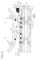
- a conductive ball mounting apparatus 2 for mounting a conductive ball on the connection pad C1 of the second wiring layers 14b on the upper surface of the wiring substrate 1 shown in Fig. 3 will be explained hereunder.
- a conductive ball mounting apparatus 2 includes a stage 30 for placing a substrate 5, and the substrate 5 is fixed on the stage 30 by vacuum contact or the like.
- the conductive ball mounting apparatus 2 also includes a mask 40 having opening portions 40a through which conductive balls pass. The mask 40 is disposed above the substrate 5.
- the mask 40 is composed of a metal mask portion 42 in which opening portions 40a are formed, a mesh portion 44 which is provided on a periphery of the metal mask portion 42, and which is made of resin or the like, and a frame portion 46 which is provided on the outer edge of the mesh portion 44.
- the mask 40 is connected to moving means (not illustrated), and is thereby capable of moving in the vertical directions and horizontal directions with high accuracy.
- the conductive ball mounting apparatus 2 includes ball supply portion 60 for supplying conductive balls 62, and the ball supply portion 60 is disposed above the mask 40.
- the conductive ball mounting apparatus 2 also includes a brush 50 (ball moving member) for sweeping and moving the large number of conductive balls 62 supplied on the mask 40 in the horizontal directions.
- the brush 50 is disposed above the mask 40.
- the brush 50 is connected to moving means (not illustrated), and is thereby capable of moving in the vertical directions and horizontal directions.
- the brush 50 is made to abut to the mask 40, and is then moved in a horizontal direction. Thereby, the conductive balls 62 on the mask 40 are transferred into the opening portions 40a of the mask 40.
- the brush 50 is given as an example of the ball moving member.
- a cylindrical brush may be moved while rotating, or a plate-like squeegee may be employed.
- the ball supply portion 60 and the ball moving member (brush 50) may be integrally provided.
- the conductive ball mounting apparatus 2 of the first embodiment further includes an adhesive film 70 (ball removing film) which removes to bond the excess conductive balls 62 remaining on the mask 40 after the conductive balls 62 are swept into the opening portions 40a of the mask 40.
- the adhesive film 70 is disposed above the mask 40.
- the adhesive film 70 is conveyed by means of a reel-to-reel system. Specifically, a roll-like film wound onto a reel (not illustrated) provided at one end side is pulled out, and is then wound onto a reel (not illustrated) provided at the other end side in a state that the film is pulled to a lower side of the two rollers 72.
- the rollers 72 or the like are connected to moving means (not illustrated), and are thereby capable of moving in the vertical directions and horizontal directions with high accuracy.
- the adhesive film 70 is disposed to be controlled at a predetermined height position from on the mask 40. Also the adhesive film 70 between the two rollers 72 is set to have a size corresponding to that of the area of the mask 40, the area in which the plural opening portions 40a are arranged. The adhesive film 70 is disposed in parallel with the mask 40. Thereafter, the excess conductive balls 62 on the mask 40 are bonded to the adhesive film 70, and the adhesive film 70 is then moved upward. Thereby, the excess conductive balls 62 are removed from the mask 40.
- the adhesive film 70 is wound onto the reel at the other end side, and the rollers 72 rotate. Thereby, the adhesive film 70 on which the conductive balls 62 are boned is moved, so that a new part of adhesive film 70 is placed under the two rollers 72.
- the adhesive film 70 is given as an example of the ball removing film.
- an electrostatic adsorption film which adsorbs the conductive balls 62 thereon by static electricity, may be employed.
- any kind of films can be employed as long as being capable of bonding the conductive balls 62 thereto and removing the conductive balls consequently.
- the conductive ball mounting apparatus 2 also includes an image recognition camera 35 which recognizes an alignment mark provided on the substrate 5, and thus has an alignment function to align such that the opening portions 40a of the mask 40 are disposed respectively above the connection pads of the substrate 5, on the basis of recognizing the alignment mark on the substrate 5.
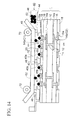
- the wiring substrate 1 is fixed to be placed on the upper surface of the stage 30 (omitted in FIG. 4 ) of the conductive ball mounting apparatus 2 shown in FIG. 13 .
- the mask 40 having the opening portions 40a described above is disposed on the wiring substrate 1.
- the image recognition camera 35 FIG. 13
- the mask 40 is aligned with the wiring substrate 1 so that the opening portions 40a of the mask 40 can correspond to the connection pads C1 of the wiring substrate 1 respectively.
- a collective recessed portion 40b is provided in the lower portion of the mask 40, the lower portion corresponding to an area where the connection pads C1 of the wiring substrate 1 are arranged with an area array type. Thereby the mask 40 is prevented from coming in contact with the fluxes 20 on the connection pads C1 of the wiring substrate 1.
- the conductive balls 62 are supplied on the mask 40 from the ball supply portion 60.
- the number of the supplied conductive balls 62 is considerably larger than that of the opening portions 40a (corresponding to the connection pads C1 of the wiring substrate 1) of the mask 40.
- a mode in which a semiconductor chip is flip-chip connected to the connection pads C1 of the wiring substrate 1 is illustrated.
- the conductive balls 62 solder balls entirely made of solder, balls composed of a core ball and a solder layer covering the outer surface of the core ball, or balls composed of a core ball made of copper and a solder layer covering the outer surface of the core ball, or the like are used.
- the conductive balls made of various conductive materials can be used depending on the usage of the substrate (work) on which conductive balls are mounted.
- the conductive balls 62 are set to have a diameter of 100 ⁇ m or less (the lower limit is 10 ⁇ m or more, for example). That is, the conductive balls 62 having a relatively small diameter, that a handling thereof is difficult in a method in which all conductive balls are mounted collectively by an adsorption tool or the like, are used.
- the large number of conductive balls 62 are moved to be swept to one end side of the mask 40 (outside the product area) by the brush 50 (ball moving member).
- the conductive balls 62 moved by the brush 50 are transferred into the opening portions 40a of the mask 40 by the brush, and are arranged to be bonded respectively to the fluxes 20 on the connection pads C1 below the opening portions 40a.
- the opening portions 40a of the mask 40 are set to have a size slightly larger than that of the conductive balls 62. Accordingly, the conductive balls 62 can easily pass through the opening portions 40a of the mask 40. In this manner, one of the conductive balls 62 is transferred into each of the opening portions 40a of the mask 40 respectively, and is arranged on the connection pad C1 of the wiring substrate 1 below the mask 40.
- the adhesive film 70 placed under the two rollers 72 described above is moved toward the mask 40. Then, as shown in FIG. 7 , the adhesive film 70 is disposed above the mask 40 while controlling the position in an extent that the adhesive film 70 does not come in contact with the mask 40, and the adhesive film 70 is made to abut onto the excess conductive balls 62 remaining on the mask 40. Thereby the excess conductive balls 62 are bonded to the adhesive film 70. Thereafter, as shown in FIG. 8 , the excess conductive balls 62 are removed from the mask 40 by moving the adhesive film 70 on which the conductive balls 62 are bonded upward.
- the conductive ball mounting apparatus 2 is provided with the adhesive film 70 disposed in parallel with the mask 40. Accordingly, although the excess conductive balls remain on the mask 40, the excess conductive balls 62 can be removed by the adhesive film 70 collectively.
- the excess conductive balls 62 can be removed collectively without repeating the movement of the brush 50 until no excess conductive balls 62 remain on the mask 40. Accordingly, the manufacturing efficiency can be remarkably improved. Moreover, unlike a method in which the conductive balls 62 are moved by blowing air, no conductive balls 62 can fly to the outside since the conductive balls are made to bond onto the adhesive film 70.
- the conductive balls 62 which are moved to the one end side of the mask 40 are left thereon as it is, and are used as part of the conductive balls to be mounted on a wiring substrate which is processed next.
- the mask 40 is also moved upward, and is consequently removed from the wiring substrate 1. Then, the adhesive film 70 is wound by the reel (not illustrated) at the other end side, and the rollers 72 are rotated, thereby a new part of adhesive film 70 is placed under the two rollers 72.
- one of the conductive balls 62 is arranged to bond to the flux 20 on each of the connection pads C1 of the wiring substrate 1 with high reliability. It should be noted that conductive balls can be mounted on the connection pads of the above-mentioned semiconductor wafer as well as the wiring substrate 1, by means of the same method.
- solder bumps 22 are obtained.
- solder bumps 80a are prepared.
- the solder bumps 80a of the semiconductor chip 80 are placed on the solder bumps 22 of the wiring substrate 1, and they are flip-chip bonding by reflow-heating.
- solder bumps 22 of the wiring substrate 1 and the solder bumps 80a of the semiconductor chip 80 are respectively fused to form bump electrodes 24.
- the semiconductor chip 80 is electrically connected to the connection pads C1 of the wiring substrate 1 via the bump electrodes 24.
- solder balls or the like are mounted on the connection pads C2 on the lower surface of the wiring substrate 1 to form external connection terminals 26.
- the timing at which the external connection terminals 26 are formed may be after the step shown in FIG. 10 (i.e. after the conductive balls 62 are mounted), or may be after the semiconductor chip 80 is mounted.
- a semiconductor device 3 according to the first embodiment is obtained.
- the wiring substrate 1 is divided to be cut, before or after the semiconductor chip 80 is mounted.
- the conductive balls 62 are arranged on the connection pads C1 of the wiring substrate 1 through the opening portions 40a of the mask 40. Thereafter, before the mask 40 is separated upward to be removed from the wiring substrate 1, the excess conductive balls 62 remaining around the opening portions 40 of the mask 40 are bonded to the adhesive film 70, and are removed consequently.
- the conductive balls 62 on the mask 40 are removed by the adhesive film 70 collectively, the conductive balls 62 can be removed more efficiently and stably than a case of employing a method in which the excess conductive balls 62 are moved on the mask 40 by a brush or air.
- the conductive balls 62 can be mounted on the wiring substrate 1 with high reliability.
- FIGS. 14 and 15 are cross-sectional views showing a method of mounting a conductive ball according to a second embodiment of the present invention.
- the same elements as those in the first embodiment are denoted by the same reference numerals, and the detailed description of those elements are omitted.
- protrusion portions 48 which protrude upward are provided on the upper surface of the mask 40.
- the protrusion portions 48 serve as stoppers for the adhesive film 70, so that the adhesive film 70 is not placed lower than the upper surfaces of the protrusion portions 48.
- the height of the protrusion portions 48 is set to be lower than the height (diameter) of the conductive balls 62.
- the height of the protrusion portions 48 is set to 20 ⁇ m to 50 ⁇ m.
- the adhesive film 70 can make the excess conductive balls 62 bond by abutting to only the excess conductive balls 62 that should be removed without coming in contact with the metal mask portion 42 of the mask 40.
- the adhesive film 70 is moved upward from the wiring substrate 1, so that the excess conductive balls 62 are removed from the mask 40, as in the first embodiment.
- the protrusion portions 48 for controlling the height position at which the adhesive film 70 is placed are provided on the mask 40, there is no possibility that the adhesive film 70 is displaced toward the mask 40. Accordingly, when the excess conductive balls 62 on the mask 40 are removed by the adhesive film 70, such a situation can be prevented that the conductive balls 62 transferred into the opening portions 40a of the mask 40 are removed simultaneously.
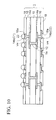
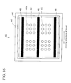
- FIG. 16 shows a state in which the mask 40 provided with the protrusion portions 48 is seen from the above.
- the opening portions 40a of the mask 40 aligned with an area array type are arranged to be divided in four areas.
- the protrusion portions 48 are provided in belt-like shapes (in stripes) so as to partition the groups of opening portions 40a located upside and downside.
- the protrusion portions 48 are each formed in a belt-like shape so as to extend in the same direction as the moving direction of the brush 50. Accordingly, the conductive balls 62 are swept to a longitudinal direction of the protrusion portions 48, and are moved to the one end side of the mask 40. Thus, there is no possibility that the protrusion portions 48 become obstacles when the conductive balls 62 are moved.
- the protrusion portions 48 may be formed integrally with the metal mask portion 42 of the mask 40, or may be formed separately from the mask 40 to be disposed on the mask 40 as spacer parts.
- the second embodiment provides the same effects as those of the first embodiment, and can improve the reliability when the excess conductive balls are removed by the adhesive film, compared to the first embodiment.
Landscapes
- Engineering & Computer Science (AREA)
- Manufacturing & Machinery (AREA)
- Microelectronics & Electronic Packaging (AREA)
- Computer Hardware Design (AREA)
- Power Engineering (AREA)
- Ceramic Engineering (AREA)
- Physics & Mathematics (AREA)
- Condensed Matter Physics & Semiconductors (AREA)
- General Physics & Mathematics (AREA)
- Mechanical Engineering (AREA)
- Electric Connection Of Electric Components To Printed Circuits (AREA)
Abstract
Description
- The present invention relates to a method of mounting a conductive ball and a conductive ball mounting apparatus, more particularly, a method of mounting a conductive ball and a conductive ball mounting apparatus, for mounting a conductive ball on a wiring substrate or the like to form a bump electrode.
- In the prior art, there has been a method of forming a solder ball on a connection pad of a wiring substrate on which a semiconductor chip or the like is to be mounted, and thereby forming a bump electrode. In such a method of mounting a solder ball, firstly, as shown in
FIG. 1A , awiring substrate 100 on which solder balls are to be mounted is prepared. In thewiring substrate 100,connection pads 200 are provided on an upper surface of asubstrate 110, and a solder resist 300 in whichopening portions 300a are provided on theconnection pads 200 is formed. Moreover, aflux 400 is coated on theconnection pads 200. - Then, as shown in
FIG. 1B , amask 500 to be used for mounting solder balls is disposed on thewiring substrate 100. Themask 500 has a configuration in which amesh portion 540 is attached to a periphery of ametal mask portion 520, and in which aframe portion 560 is provided on the outer edge of themesh portion 540. Moreover, openingportions 500a through which solder balls pass are formed in parts of themask portion 520, the parts corresponding to theconnection pads 200 of thewiring substrate 100. - Next, as shown in
Fig. 1B similarly, a large number ofsolder balls 600 are supplied onto themask 500 and then swept to move to one end side of themask 500 by abrush 700. Thereby, as shown inFig. 1C , thesolder balls 600 pass through theopening portions 500a of themask 500 and are arranged to be bonded to thefluxes 400 on theconnection pads 200 of thewiring substrate 100. Thereafter, themask 500 is moved upward to be removed from thewiring substrate 100. - Otherwise, as shown in
FIG. 2 , there is another method using anair supply 750 instead of the use of thebrush 700. In this method, by blowing air to thesolder balls 600 from anair supply 750 to move thesolder balls 600 to one end side of themask 500, thesolder balls 600 is arranged on theconnection pads 200 of thewiring substrate 100 while causing thesolder balls 600 to pass through theopening portions 500a of themask 500. - As the techniques related to the above-described methods of mounting a solder ball, in Patent Literature 1 (Japanese Patent Application Publication No.
2004-186286 - Also, in Patent Literature 2 (Japanese Patent Application Publication No.
2006-173195 - In the above-described prior arts, the
solder balls 600 the number of which is considerably larger than that of theopening portions 500a of themask 500 are supplied on themask 500. Accordingly, although some of thesolder balls 600 pass through theopening portions 500a of themask 500, someother solder balls 600 remain around theopening portions 500a of themask 500 in many cases. Such being the case, it is necessary to move theexcess solder balls 600 to one end side of themask 500, or to remove theexcess solder balls 600 from themask 500. - Without this operation, the
excess solder balls 600 remaining on themask 500 may pass through theopening portions 500a of themask 500 when themask 500 is moved upward from thewiring substrate 100 to be separated therefrom, and consequently, multiple solder balls are likely to be mounted on theconnection pads 200 of thewiring substrate 100, in some cases. - In the method in which the excess solder balls on the mask are moved by the brush, the brush needs to be moved repeatedly with many times in order to remove all the excess solder balls. Consequently, a long time is required for the operation, and, hence, the manufacturing efficiency is low. Furthermore, solder balls sometimes adhere to the brush, which is likely to complicate the maintenance.
- In the method in which the excess solder balls on the mask are moved by using air, the wind pressure needs to be set relatively high in order to efficiently move the solder balls. As a result, solder balls on the mask sometimes fly to the outside of the mask in some cases. By contrast, when the wind pressure is set low enough to prevent solder balls from flying to the outside, it is extremely difficult to move all the excess solder balls.
- It is desirable to provided a method of mounting a conductive ball and a conductive ball mounting apparatus which are capable of mounting conductive balls with high reliability while efficiently removing excess conductive balls on a mask, in a method for mounting the conductive balls on a substrate through the mask.
- According to an embodiment of a first aspect of the present invention there is provided a method of mounting a conductive ball, which method includes the steps of: disposing a mask on a substrate including connection pads, the mask having opening portions corresponding to the connection pads; supplying conductive balls on the mask; arranging the conductive balls on the connection pad of the substrate through the opening portion of the mask, by moving the conductive balls to one end side of the mask by a ball moving member; and removing excess conductive balls remaining on a region of the mask where the opening portions are provided, by bonding the excess conductive balls to a ball removal film.
- In a method of mounting a conductive ball embodying the present invention, firstly, a mask is disposed on a substrate (such as a wiring substrate, or a semiconductor wafer in which semiconductor element is made) having connection pads, the mask having opening portions corresponding to the connection pads. Thereafter, a larger number of conductive balls (solder balls or the like) than that of the opening portions are supplied on the mask.
- Then, the conductive balls are swept and moved to one end side of the mask by moving ball moving member (a brush or the like) in a horizontal direction. Thereby, the conductive balls pass through the opening portions of the mask, and are arranged respectively on the connection pads of the substrate. At this stage, some of the conductive balls remain as excess in regions in which the opening portions are formed, on the mask.
- Subsequently, the excess conductive balls on the mask are bonded to a ball removing film (such as an adhesive film or an electrostatic adsorption film), thereby the excess conductive balls are removed from the mask consequently.
- In an embodiment of the present invention, unlike the prior arts, makes it possible collectively to remove the excess conductive balls by using the ball removal film without moving the brush repeatedly until no excess conductive balls remain on the mask. Accordingly, the manufacturing efficiency can be remarkably improved. Moreover, unlike a method in which the conductive balls are moved by blowing air, no conductive balls can fly to the outside since the conductive balls are bonded to the adhesive film and are then removed.
- In addition, since no excess conductive balls remain around the opening portions of the mask, this method prevents the excess conductive balls from being mounted on the substrate through the opening portions of the mask when the mask is moved upward to be removed from the substrate. Accordingly, a single conductive ball can be mounted on each of the connection pads of the substrate with high reliability.
- According to one preferred embodiment of the present invention, the ball removal film is placed in parallel with the mask in a state that a roll-like film is pulled out. After the conductive balls adhere to the ball removal film and are then removed, a used part of the film is wound, and a new part of the ball removal film is placed on the mask.
- In an embodiment of the present invention described above, a protrusion portion protruding upward may be provided on an upper surface of the mask. According to this embodiment, even when the ball removal film is displaced closer to the mask, the protrusion portion serves as a stopper, so that the height position of the ball removal film is controlled to be a desired position. Thus, only the excess conductive balls on the mask are selectively removed in a stable manner without removing the conductive balls passing through the opening portions of the mask.
- As described above, in an embodiment of the present invention, conductive balls can be mounted on a substrate with high reliability while excess conductive balls on the mask are removed efficiently.
-
-
FIGS. 1A to 1C are cross-sectional views showing a method (first method) of mounting a conductive ball, according to the prior art. -
FIG. 2 is a cross-sectional view showing a method (second method) of mounting a conductive ball, according to the prior art. -
FIG. 3 is a cross-sectional view (No. 1) showing a method of mounting a conductive ball, according to a first embodiment of the present invention. -
FIG. 4 is a cross-sectional view (No. 2) showing the method of mounting a conductive ball, according to the first embodiment of the present invention. -
FIG. 5 is a cross-sectional view (No. 3) showing the method of mounting a conductive ball, according to the first embodiment of the present invention. -
FIG. 6 is a cross-sectional view (No. 4) showing the method of mounting a conductive ball, according to the first embodiment of the present invention. -
FIG. 7 is a cross-sectional view (No. 5) showing the method of mounting a conductive ball, according to the first embodiment of the present invention. -
FIG. 8 is a cross-sectional view (No. 6) showing the method of mounting a conductive ball, according to the first embodiment of the present invention. -
FIG. 9 is a cross-sectional view (No. 7) showing the method of mounting a conductive ball, according to the first embodiment of the present invention. -
FIG. 10 is a cross-sectional view (No. 1) showing a method for mounting a semiconductor chip on a wiring substrate on which conductive balls are mounted. -
FIG. 11 is a cross-sectional view (No. 2) showing the method for mounting a semiconductor chip on a wiring substrate on which conductive balls are mounted. -
FIG. 12 is a cross-sectional view (No. 3) showing the method for mounting a semiconductor chip on a wiring substrate on which conductive balls are mounted. -
FIG. 13 is a cross sectional view showing a conductive ball mounting apparatus according to the first embodiment of the present invention. -
FIG. 14 is a cross-sectional view (No. 1) showing a method of mounting a conductive ball, according to a second embodiment of the present invention. -
FIG. 15 is a cross-sectional view (No. 2) showing the method of mounting a conductive ball, according to the second embodiment of the present invention. -
FIG. 16 is a plan view showing a state of a mask on which protrusion portions are provided, according to the second embodiment of the present invention. - Description will be given below of embodiments of the present invention with reference to the accompanying drawings.
-
FIGS. 3 to 9 are cross-sectional views showing a method of mounting a conductive ball, according to a first embodiment of the present invention;FIGS. 10 to 12 are cross-sectional views showing a method of mounting a semiconductor chip on a wiring substrate on which conductive balls are mounted; andFIG. 13 is a cross-sectional view showing a conductive ball mounting apparatus similarly. - In the method of mounting a conductive ball, according to the first embodiment, firstly, as shown in
FIG. 3 , awiring substrate 1 on which conductive balls are to be mounted is prepared. In thewiring substrate 1, through holes TH are formed in acore substrate 10 made of glass epoxy resin or the like, and the through holes TH are filled respectively with through-hole electrodes 12 made of copper or the like. In addition,first wiring layers 14a connected to each other via through-hole electrode 12 and made of copper, are respectively formed on both surfaces of thecore substrate 10. - Alternatively, the
first wiring layers 14a which are formed on the both surfaces of thecore substrate 10, may be connected to each other with a through-hole plated layer formed on an inner wall of the through holes TH, and the opening in the through holes TH may be filled with resin. - On the both surfaces of the
core substrate 10,interlayer insulating films 16 for covering thefirst wiring layers 14a are formed respectively. Theinterlayer insulating films 16 are formed by affixing resin films made of epoxy, polyimide or the like to thecore substrate 10, for example. - In the
interlayer insulating layers 16 on the both surfaces of thecore substrate 10, via holes VH having a depth which reaches thefirst wiring layer 14a are formed respectively. Moreover, on theinterlayer insulating layers 16 on the both surfaces of thecore substrate 10, the second wiring layers 14b connected to the first wiring layers 14a through the via holes VH are formed respectively. InFIG. 3 , connection pads C1 and C2 are shown as the second wiring layers 14b. - A solder resist 18 in which an
opening portion 18a is provided on each of the connection pads C1, C2 is formed on the second wiring layers 14b on both surfaces of thecore substrate 10 respectively. In addition, fluxes 20 are formed respectively on the connection pads C1 of the second wiring layers 14b on the upper surface of thecore substrate 10. Thefluxes 20 are coated to be patterned on the connection pads C1 of the second wiring layers 14b by means of printing or a dispenser. - Here, a rigid substrate is given as an example of the
wiring substrate 1. However, a flexible wiring substrate, which uses a film as a substrate, may be used as thewiring substrate 1. - Alternatively, as a substrate (work) on which the conductive balls are to be mounted, instead of the
wiring substrate 1, a semiconductor wafer (silicon wafer) on which a semiconductor element (a transistor or the like) and multilayer wiring layers connected to the semiconductor element are formed and connection pads are provided on an uppermost layer, may be used. Such semiconductor wafer is diced after the conductive balls are mounted on the connection pads thereof, thereby an individual semiconductor chip such as a CPU, a memory, or the like is obtained. - Next, a conductive ball mounting apparatus for mounting a conductive ball on the connection pad C1 of the second wiring layers 14b on the upper surface of the
wiring substrate 1 shown inFig. 3 will be explained hereunder. As shown inFIG. 13 , a conductive ball mounting apparatus 2 according to the first embodiment includes astage 30 for placing asubstrate 5, and thesubstrate 5 is fixed on thestage 30 by vacuum contact or the like. Moreover, the conductive ball mounting apparatus 2 also includes amask 40 havingopening portions 40a through which conductive balls pass. Themask 40 is disposed above thesubstrate 5. - The
mask 40 is composed of ametal mask portion 42 in which openingportions 40a are formed, amesh portion 44 which is provided on a periphery of themetal mask portion 42, and which is made of resin or the like, and aframe portion 46 which is provided on the outer edge of themesh portion 44. Themask 40 is connected to moving means (not illustrated), and is thereby capable of moving in the vertical directions and horizontal directions with high accuracy. - Furthermore, the conductive ball mounting apparatus 2 includes
ball supply portion 60 for supplyingconductive balls 62, and theball supply portion 60 is disposed above themask 40. The conductive ball mounting apparatus 2 also includes a brush 50 (ball moving member) for sweeping and moving the large number ofconductive balls 62 supplied on themask 40 in the horizontal directions. Thebrush 50 is disposed above themask 40. - The
brush 50 is connected to moving means (not illustrated), and is thereby capable of moving in the vertical directions and horizontal directions. Thebrush 50 is made to abut to themask 40, and is then moved in a horizontal direction. Thereby, theconductive balls 62 on themask 40 are transferred into the openingportions 40a of themask 40. - Here, the
brush 50 is given as an example of the ball moving member. However, a cylindrical brush may be moved while rotating, or a plate-like squeegee may be employed. Alternatively, theball supply portion 60 and the ball moving member (brush 50) may be integrally provided. - Moreover, the conductive ball mounting apparatus 2 of the first embodiment further includes an adhesive film 70 (ball removing film) which removes to bond the excess
conductive balls 62 remaining on themask 40 after theconductive balls 62 are swept into the openingportions 40a of themask 40. Theadhesive film 70 is disposed above themask 40. - The
adhesive film 70 is conveyed by means of a reel-to-reel system. Specifically, a roll-like film wound onto a reel (not illustrated) provided at one end side is pulled out, and is then wound onto a reel (not illustrated) provided at the other end side in a state that the film is pulled to a lower side of the tworollers 72. Therollers 72 or the like are connected to moving means (not illustrated), and are thereby capable of moving in the vertical directions and horizontal directions with high accuracy. - By this matter, the
adhesive film 70 is disposed to be controlled at a predetermined height position from on themask 40. Also theadhesive film 70 between the tworollers 72 is set to have a size corresponding to that of the area of themask 40, the area in which theplural opening portions 40a are arranged. Theadhesive film 70 is disposed in parallel with themask 40. Thereafter, the excessconductive balls 62 on themask 40 are bonded to theadhesive film 70, and theadhesive film 70 is then moved upward. Thereby, the excessconductive balls 62 are removed from themask 40. - Then, the
adhesive film 70 is wound onto the reel at the other end side, and therollers 72 rotate. Thereby, theadhesive film 70 on which theconductive balls 62 are boned is moved, so that a new part ofadhesive film 70 is placed under the tworollers 72. - Here, the
adhesive film 70 is given as an example of the ball removing film. However, an electrostatic adsorption film, which adsorbs theconductive balls 62 thereon by static electricity, may be employed. Thus, any kind of films can be employed as long as being capable of bonding theconductive balls 62 thereto and removing the conductive balls consequently. - Furthermore, the conductive ball mounting apparatus 2 also includes an
image recognition camera 35 which recognizes an alignment mark provided on thesubstrate 5, and thus has an alignment function to align such that the openingportions 40a of themask 40 are disposed respectively above the connection pads of thesubstrate 5, on the basis of recognizing the alignment mark on thesubstrate 5. - Next, a method of mounting a conductive ball on the connection pads C1 of the above-described wiring substrate 1 (
FIG. 3 ) by using the conductive ball mounting apparatus 2 described above will be explained hereunder. As shown inFIG. 4 , firstly, thewiring substrate 1 is fixed to be placed on the upper surface of the stage 30 (omitted inFIG. 4 ) of the conductive ball mounting apparatus 2 shown inFIG. 13 . - Then, the
mask 40 having the openingportions 40a described above is disposed on thewiring substrate 1. In this event, the image recognition camera 35 (FIG. 13 ) described above recognizes the alignment mark of thewiring substrate 1. Thereby, themask 40 is aligned with thewiring substrate 1 so that the openingportions 40a of themask 40 can correspond to the connection pads C1 of thewiring substrate 1 respectively. - In addition, a collective recessed
portion 40b is provided in the lower portion of themask 40, the lower portion corresponding to an area where the connection pads C1 of thewiring substrate 1 are arranged with an area array type. Thereby themask 40 is prevented from coming in contact with thefluxes 20 on the connection pads C1 of thewiring substrate 1. - Subsequently, as shown in
FIG. 4 , theconductive balls 62 are supplied on themask 40 from theball supply portion 60. The number of the suppliedconductive balls 62 is considerably larger than that of the openingportions 40a (corresponding to the connection pads C1 of the wiring substrate 1) of themask 40. - In the first embodiment, a mode in which a semiconductor chip is flip-chip connected to the connection pads C1 of the
wiring substrate 1 is illustrated. In such a case, as theconductive balls 62, solder balls entirely made of solder, balls composed of a core ball and a solder layer covering the outer surface of the core ball, or balls composed of a core ball made of copper and a solder layer covering the outer surface of the core ball, or the like are used. The conductive balls made of various conductive materials can be used depending on the usage of the substrate (work) on which conductive balls are mounted. - Moreover, in the first embodiment, the
conductive balls 62 are set to have a diameter of 100 µm or less (the lower limit is 10 µm or more, for example). That is, theconductive balls 62 having a relatively small diameter, that a handling thereof is difficult in a method in which all conductive balls are mounted collectively by an adsorption tool or the like, are used. Here, when the diameter of theconductive balls 62 is 100 µm, for example, a pitch between the connection pads C1 of thewiring substrate 1 is 200 µm (line:space = 100:100 µm). - Then, as shown in
FIG. 5 , the large number ofconductive balls 62 are moved to be swept to one end side of the mask 40 (outside the product area) by the brush 50 (ball moving member). In this event, theconductive balls 62 moved by thebrush 50 are transferred into the openingportions 40a of themask 40 by the brush, and are arranged to be bonded respectively to thefluxes 20 on the connection pads C1 below the openingportions 40a. - The opening
portions 40a of themask 40 are set to have a size slightly larger than that of theconductive balls 62. Accordingly, theconductive balls 62 can easily pass through the openingportions 40a of themask 40. In this manner, one of theconductive balls 62 is transferred into each of the openingportions 40a of themask 40 respectively, and is arranged on the connection pad C1 of thewiring substrate 1 below themask 40. - Also in this event, even if the large number of the
conductive balls 62 are moved to the one end side of themask 40 by thebrush 50, some of theconductive balls 62 remain in the regions in which theplural opening portions 40a are arranged (around the openingportions 40a), on themask 40. In order to prevent theconductive balls 62 from remaining around the openingportions 40a of themask 40, thebrush 50 needs to be moved repeatedly with many times. Consequently, a long time is required for the operation, and hence, the manufacturing efficiency is low. - In consideration of this, in the first embodiment, as shown in
FIG. 6 , theadhesive film 70 placed under the tworollers 72 described above is moved toward themask 40. Then, as shown inFIG. 7 , theadhesive film 70 is disposed above themask 40 while controlling the position in an extent that theadhesive film 70 does not come in contact with themask 40, and theadhesive film 70 is made to abut onto the excessconductive balls 62 remaining on themask 40. Thereby the excessconductive balls 62 are bonded to theadhesive film 70. Thereafter, as shown inFIG. 8 , the excessconductive balls 62 are removed from themask 40 by moving theadhesive film 70 on which theconductive balls 62 are bonded upward. - As described above, in the first embodiment, the conductive ball mounting apparatus 2 is provided with the
adhesive film 70 disposed in parallel with themask 40. Accordingly, although the excess conductive balls remain on themask 40, the excessconductive balls 62 can be removed by theadhesive film 70 collectively. - Hence, unlike the prior arts, the excess
conductive balls 62 can be removed collectively without repeating the movement of thebrush 50 until no excessconductive balls 62 remain on themask 40. Accordingly, the manufacturing efficiency can be remarkably improved. Moreover, unlike a method in which theconductive balls 62 are moved by blowing air, noconductive balls 62 can fly to the outside since the conductive balls are made to bond onto theadhesive film 70. - Note that, the
conductive balls 62 which are moved to the one end side of themask 40 are left thereon as it is, and are used as part of the conductive balls to be mounted on a wiring substrate which is processed next. - Subsequently, as shown in
FIG. 9 , after theadhesive film 70 is moved upward, themask 40 is also moved upward, and is consequently removed from thewiring substrate 1. Then, theadhesive film 70 is wound by the reel (not illustrated) at the other end side, and therollers 72 are rotated, thereby a new part ofadhesive film 70 is placed under the tworollers 72. - Here, no excess
conductive balls 62 are left around the openingportions 40a of themask 40 when themask 40 is separated from thewiring substrate 1. Hence, the problem that the pluralconductive balls 62 are mounted on each of the connection pads C1 of thewiring substrate 1 is solved. - By this matter, one of the
conductive balls 62 is arranged to bond to theflux 20 on each of the connection pads C1 of thewiring substrate 1 with high reliability. It should be noted that conductive balls can be mounted on the connection pads of the above-mentioned semiconductor wafer as well as thewiring substrate 1, by means of the same method. - Next, a method of mounting a semiconductor chip on the
wiring substrate 1 on which theconductive balls 62 are mounted will be explained. As shown inFIG. 10 , the conductive balls 62 (solder balls) are reflow-heated, then remaining fluxes are removed, thereby solder bumps 22 are obtained. Thereafter, as shown inFIG. 11 , asemiconductor chip 80 havingsolder bumps 80a is prepared. The solder bumps 80a of thesemiconductor chip 80 are placed on the solder bumps 22 of thewiring substrate 1, and they are flip-chip bonding by reflow-heating. - Thereby, as shown in
FIG. 12 , the solder bumps 22 of thewiring substrate 1 and the solder bumps 80a of thesemiconductor chip 80 are respectively fused to formbump electrodes 24. Thus, thesemiconductor chip 80 is electrically connected to the connection pads C1 of thewiring substrate 1 via thebump electrodes 24. In addition, solder balls or the like are mounted on the connection pads C2 on the lower surface of thewiring substrate 1 to formexternal connection terminals 26. - The timing at which the
external connection terminals 26 are formed may be after the step shown inFIG. 10 (i.e. after theconductive balls 62 are mounted), or may be after thesemiconductor chip 80 is mounted. - By this matter, a
semiconductor device 3 according to the first embodiment is obtained. In a case where a large-sized substrate for multiple productions is used as thewiring substrate 1, thewiring substrate 1 is divided to be cut, before or after thesemiconductor chip 80 is mounted. - As described above, in the method of mounting a conductive ball, according to the first embodiment, firstly, the
conductive balls 62 are arranged on the connection pads C1 of thewiring substrate 1 through the openingportions 40a of themask 40. Thereafter, before themask 40 is separated upward to be removed from thewiring substrate 1, the excessconductive balls 62 remaining around the openingportions 40 of themask 40 are bonded to theadhesive film 70, and are removed consequently. - Accordingly, since the excess
conductive balls 62 on themask 40 are removed by theadhesive film 70 collectively, theconductive balls 62 can be removed more efficiently and stably than a case of employing a method in which the excessconductive balls 62 are moved on themask 40 by a brush or air. - Moreover, since no excess
conductive balls 62 remain around the openingportions 40a of themask 40, such a situation is prevented that the pluralconductive balls 62 are mounted on each of the connection pads C1 of thewiring substrate 1. Accordingly, theconductive balls 62 can be mounted on thewiring substrate 1 with high reliability. -
FIGS. 14 and15 are cross-sectional views showing a method of mounting a conductive ball according to a second embodiment of the present invention. In the second embodiment, the same elements as those in the first embodiment are denoted by the same reference numerals, and the detailed description of those elements are omitted. - In the above-described method of mounting a conductive ball according to the first embodiment, by directly disposing the
adhesive film 70 on themask 40 which is flat while controlling the height position, the excessconductive balls 62 on themask 40 are removed to be bonded to theadhesive film 70 - By this matter, in the case where the
adhesive film 70 is displaced toward themask 40 and is consequently placed in contact with themask 40, it is assumed that not only the excessconductive balls 62 on themask 40 but also theconductive balls 62 transferred into the openingportions 40 of themask 40 are removed to be bonded to theadhesive film 70 simultaneously. - To prevent this, in the second embodiment, as shown in
FIG. 14 ,protrusion portions 48 which protrude upward are provided on the upper surface of themask 40. Hence, theprotrusion portions 48 serve as stoppers for theadhesive film 70, so that theadhesive film 70 is not placed lower than the upper surfaces of theprotrusion portions 48. - The height of the
protrusion portions 48 is set to be lower than the height (diameter) of theconductive balls 62. For example, when the height (diameter) of theconductive balls 62 is 100 µm, the height of theprotrusion portions 48 is set to 20 µm to 50 µm. Theadhesive film 70 can make the excessconductive balls 62 bond by abutting to only the excessconductive balls 62 that should be removed without coming in contact with themetal mask portion 42 of themask 40. - Thereafter, as shown in
FIG. 15 , theadhesive film 70 is moved upward from thewiring substrate 1, so that the excessconductive balls 62 are removed from themask 40, as in the first embodiment. - As described above, in the second embodiment, since the
protrusion portions 48 for controlling the height position at which theadhesive film 70 is placed are provided on themask 40, there is no possibility that theadhesive film 70 is displaced toward themask 40. Accordingly, when the excessconductive balls 62 on themask 40 are removed by theadhesive film 70, such a situation can be prevented that theconductive balls 62 transferred into the openingportions 40a of themask 40 are removed simultaneously. -
FIG. 16 shows a state in which themask 40 provided with theprotrusion portions 48 is seen from the above. In the example shown inFIG. 16 , the openingportions 40a of themask 40 aligned with an area array type are arranged to be divided in four areas. Theprotrusion portions 48 are provided in belt-like shapes (in stripes) so as to partition the groups of openingportions 40a located upside and downside. - In other words, the
protrusion portions 48 are each formed in a belt-like shape so as to extend in the same direction as the moving direction of thebrush 50. Accordingly, theconductive balls 62 are swept to a longitudinal direction of theprotrusion portions 48, and are moved to the one end side of themask 40. Thus, there is no possibility that theprotrusion portions 48 become obstacles when theconductive balls 62 are moved. - The
protrusion portions 48 may be formed integrally with themetal mask portion 42 of themask 40, or may be formed separately from themask 40 to be disposed on themask 40 as spacer parts. - Then, similarly to the first embodiment, after the
mask 40 is moved upward from thewiring substrate 1 and is then removed inFig. 15 , the same steps as those shown inFIGS. 10 to 12 described above are performed. By this matter, a semiconductor chip is mounted on thewiring substrate 1 by flip-chip mounting, and a semiconductor device is composed. - The second embodiment provides the same effects as those of the first embodiment, and can improve the reliability when the excess conductive balls are removed by the adhesive film, compared to the first embodiment.
Claims (10)
- A method of mounting a conductive ball, comprising the steps of:disposing a mask (40) on a substrate (1) including connection pads (C1), the mask (40) having opening portions (40a) corresponding to the connection pads (C1);supplying conductive balls (62) on the mask (40) ;arranging the conductive balls (62) on the connection pad (C1) of the substrate (1) through the opening portion (40a)of the mask (40), by moving the conductive balls (62) to one end side of the mask (40) by a ball moving member (50); andremoving excess conductive balls (62) remaining on a region of the mask (40) where the opening portions (40a) are provided, by bonding the excess conductive balls (62) to a ball removal film (70).
- The method of mounting a conductive ball according to claim 1, wherein the ball removal film (70) is any one of an adhesive film and an electrostatic adsorption film.
- The method of mounting a conductive ball according to claim 1 or 2, wherein in the ball removal film (70), a roll-like film is pulled out to be placed in parallel with the mask, and after the conductive balls(62) are removed to be bonded to the ball removal film (70), the ball removal film (70) is wound, and a new part of the ball removal film (70) is placed on the mask (40).
- The method of mounting a conductive ball according to claim 1, 2 or 3, wherein the substrate(1) is any one of a wiring substrate for mounting a semiconductor chip, and a semiconductor wafer in which a semiconductor element is made.
- The method of mounting a conductive ball according to any preceding claim, wherein a protrusion portion (48) protruding upward is provided on an upper surface of the mask (40), and the ball removal film (70) is placed on the protrusion potion (48), so that the height position of the ball removal film (70) is controlled.
- The method of mounting a conductive ball according to claim 5, wherein the protrusion portion (48) is provided in a belt-like shape in the same direction as the moving direction of the ball moving member (50).
- A conductive ball mounting apparatus comprising:a stage (30) for placing a substrate (5);a mask (40) which is disposed on the substrate (5), and in which opening portions (40a) are provided;a ball supply portion (60) supplying conductive balls (62) on the mask (40);a ball moving member (50) for arranging the conductive balls (62) on the connection pad (C1) of the substrate (1) through the opening portion (40a) of the mask (40), by moving the conductive balls (62) to one end side of the mask (40) by the ball moving member(50); anda ball removal film (70) for removing excess conductive balls (62) remaining on a region of the mask (40) where the opening portions (40a) are provided, by bonding the excess conductive balls (62) after the conductive balls (62) on the mask (40) are moved.
- The conductive ball mounting apparatus according to claim 7, wherein the ball removal film (70) is any one of an adhesive film and an electrostatic adsorption film.
- The conductive ball mounting apparatus according to claim 7 or 8, wherein in the ball removal film (70), a roll-like film is pulled out to be placed in parallel with the mask (40), and after the conductive balls (62) are removed to be bonded to the ball removal film (70), the ball removal film (70) is wound, and a new part of the ball removal film (70) is placed on the mask.
- The conductive ball mounting apparatus according to claim 7, 8 or 9, wherein a protrusion portion (48) protruding upward is provided on an upper surface of the mask (40), and the ball removal film (70) is placed on the protrusion portion (48), so that the height position of the ball removal film (70) is controlled.
Applications Claiming Priority (1)
| Application Number | Priority Date | Filing Date | Title |
|---|---|---|---|
| JP2007239045A JP4444322B2 (en) | 2007-09-14 | 2007-09-14 | Conductive ball mounting method and conductive ball mounting apparatus |
Publications (3)
| Publication Number | Publication Date |
|---|---|
| EP2037493A2 true EP2037493A2 (en) | 2009-03-18 |
| EP2037493A3 EP2037493A3 (en) | 2011-09-14 |
| EP2037493B1 EP2037493B1 (en) | 2013-11-13 |
Family
ID=40278956
Family Applications (1)
| Application Number | Title | Priority Date | Filing Date |
|---|---|---|---|
| EP08161922.3A Active EP2037493B1 (en) | 2007-09-14 | 2008-08-06 | Method of mounting conductive ball and conductive ball mounting apparatus |
Country Status (3)
| Country | Link |
|---|---|
| US (1) | US7854366B2 (en) |
| EP (1) | EP2037493B1 (en) |
| JP (1) | JP4444322B2 (en) |
Families Citing this family (16)
| Publication number | Priority date | Publication date | Assignee | Title |
|---|---|---|---|---|
| JP4828595B2 (en) * | 2007-12-19 | 2011-11-30 | 新光電気工業株式会社 | Conductive ball removing method and conductive ball removing apparatus |
| JP5181390B2 (en) * | 2008-06-30 | 2013-04-10 | 澁谷工業株式会社 | Ball mounting device |
| JP2010021445A (en) * | 2008-07-11 | 2010-01-28 | Nippon Steel Materials Co Ltd | Micro-ball removal method and removal device, and micro-ball batch mounting method and batch mounting device |
| US8875978B2 (en) * | 2012-02-11 | 2014-11-04 | International Business Machines Corporation | Forming constant diameter spherical metal balls |
| US8561880B2 (en) * | 2012-02-11 | 2013-10-22 | International Business Machines Corporation | Forming metal preforms and metal balls |
| JP5886120B2 (en) * | 2012-04-25 | 2016-03-16 | 富士機械製造株式会社 | Squeegee and conductive ball supply device provided with squeegee |
| US8523046B1 (en) * | 2012-10-18 | 2013-09-03 | International Business Machines Corporation | Forming an array of metal balls or shapes on a substrate |
| KR102029077B1 (en) | 2013-02-04 | 2019-10-07 | 삼성전자주식회사 | Method of forming external terminals of a package and apparatus for performing the same |
| JP6109609B2 (en) | 2013-03-14 | 2017-04-05 | Aiメカテック株式会社 | Solder ball printing machine and solder ball printing method |
| KR102100867B1 (en) * | 2013-06-26 | 2020-04-14 | 삼성전자주식회사 | Apparatus of Mounting Solder Balls |
| JP6381322B2 (en) * | 2014-07-07 | 2018-08-29 | マクセルホールディングス株式会社 | Mask for array |
| US9905525B1 (en) * | 2016-08-18 | 2018-02-27 | Semiconductor Components Industries, Llc | Semiconductor wafer and method of ball drop on thin wafer with edge support ring |
| JP2019206088A (en) * | 2018-05-28 | 2019-12-05 | 株式会社ボンマーク | Mask for alignment of ball and manufacturing method therefor |
| KR102078936B1 (en) * | 2018-11-07 | 2020-02-19 | 주식회사 프로텍 | Method of Mounting Conductive Ball |
| KR102078935B1 (en) * | 2018-11-07 | 2020-02-19 | 주식회사 프로텍 | Apparatus for Mounting Conductive Ball |
| JP7468943B1 (en) | 2023-01-30 | 2024-04-16 | アスリートFa株式会社 | Ball mounting device and ball mounting method |
Citations (2)
| Publication number | Priority date | Publication date | Assignee | Title |
|---|---|---|---|---|
| JP2004186286A (en) | 2002-12-02 | 2004-07-02 | Casio Comput Co Ltd | Method of forming metal bowl |
| JP2006173195A (en) | 2004-12-13 | 2006-06-29 | Athlete Fa Kk | Arrangement method and device of minute particles |
Family Cites Families (6)
| Publication number | Priority date | Publication date | Assignee | Title |
|---|---|---|---|---|
| US6191022B1 (en) * | 1999-04-18 | 2001-02-20 | Cts Corporation | Fine pitch solder sphere placement |
| SG99331A1 (en) * | 2000-01-13 | 2003-10-27 | Hitachi Ltd | Method of producing electronic part with bumps and method of producing elctronic part |
| JP2005056901A (en) * | 2003-08-04 | 2005-03-03 | Nippon Steel Corp | Apparatus and process for manufacturing semiconductor device |
| JP2005158944A (en) * | 2003-11-25 | 2005-06-16 | Renesas Technology Corp | Semiconductor device manufacturing method |
| DE102004025279B4 (en) | 2004-05-19 | 2011-04-28 | Infineon Technologies Ag | System for equipping substrates with ball contacts and method for equipping substrates with ball contacts |
| WO2007123384A1 (en) * | 2006-04-25 | 2007-11-01 | Gutierrez Garcia Jose Luis | Tool for dry cleaning misprinted electronic cards |
-
2007
- 2007-09-14 JP JP2007239045A patent/JP4444322B2/en active Active
-
2008
- 2008-08-06 EP EP08161922.3A patent/EP2037493B1/en active Active
- 2008-08-08 US US12/188,556 patent/US7854366B2/en active Active
Patent Citations (2)
| Publication number | Priority date | Publication date | Assignee | Title |
|---|---|---|---|---|
| JP2004186286A (en) | 2002-12-02 | 2004-07-02 | Casio Comput Co Ltd | Method of forming metal bowl |
| JP2006173195A (en) | 2004-12-13 | 2006-06-29 | Athlete Fa Kk | Arrangement method and device of minute particles |
Also Published As
| Publication number | Publication date |
|---|---|
| EP2037493A3 (en) | 2011-09-14 |
| JP2009071109A (en) | 2009-04-02 |
| JP4444322B2 (en) | 2010-03-31 |
| US20090072011A1 (en) | 2009-03-19 |
| US7854366B2 (en) | 2010-12-21 |
| EP2037493B1 (en) | 2013-11-13 |
Similar Documents
| Publication | Publication Date | Title |
|---|---|---|
| EP2037493B1 (en) | Method of mounting conductive ball and conductive ball mounting apparatus | |
| US9305862B2 (en) | Support mounted electrically interconnected die assembly | |
| CN102386197B (en) | Image sensor chip package and method for forming the same | |
| JP5014853B2 (en) | Manufacturing method of semiconductor device | |
| JP4393538B2 (en) | Magnetic solder ball arrangement apparatus and arrangement method | |
| US8115300B2 (en) | Wiring substrate and manufacturing method thereof, and semiconductor apparatus | |
| US7432114B2 (en) | Semiconductor device manufacturing method | |
| US20110057327A1 (en) | Semiconductor device and method of manufacturing the same | |
| US20090130838A1 (en) | Method of forming conductive bumps | |
| US8141770B2 (en) | Conductive ball mounting method and surplus ball removing apparatus | |
| JPH07321244A (en) | Electronic part, and manufacture of electronic part | |
| US20070187827A1 (en) | Semiconductor package, stack package using the same package and method of fabricating the same | |
| JP2009188260A (en) | Semiconductor device and mounting substrate | |
| JP4206779B2 (en) | Manufacturing method of semiconductor device | |
| JP2005026346A (en) | Lamination method of semiconductor chip | |
| US11482502B2 (en) | Semiconductor device and semiconductor device manufacturing method | |
| TW201842632A (en) | Package method including forming electrical paths through a mold layer | |
| JP2009147250A (en) | Conductive ball mounting method and conductive ball mounting apparatus | |
| JP2009146963A (en) | Mounting method for conductive ball and conductive ball mounting device | |
| TWI778918B (en) | Manufacturing method of semiconductor device and semiconductor device | |
| US20220367230A1 (en) | Micro device structure and display apparatus | |
| TW201030935A (en) | Semiconductor die interconnect formed by aerosol application of electrically conductive material | |
| JP2007049183A (en) | Semiconductor device | |
| JP4297153B2 (en) | Manufacturing method of semiconductor device | |
| JP2007043194A (en) | Semiconductor device |
Legal Events
| Date | Code | Title | Description |
|---|---|---|---|
| PUAI | Public reference made under article 153(3) epc to a published international application that has entered the european phase |
Free format text: ORIGINAL CODE: 0009012 |
|
| AK | Designated contracting states |
Kind code of ref document: A2 Designated state(s): AT BE BG CH CY CZ DE DK EE ES FI FR GB GR HR HU IE IS IT LI LT LU LV MC MT NL NO PL PT RO SE SI SK TR |
|
| AX | Request for extension of the european patent |
Extension state: AL BA MK RS |
|
| PUAL | Search report despatched |
Free format text: ORIGINAL CODE: 0009013 |
|
| AK | Designated contracting states |
Kind code of ref document: A3 Designated state(s): AT BE BG CH CY CZ DE DK EE ES FI FR GB GR HR HU IE IS IT LI LT LU LV MC MT NL NO PL PT RO SE SI SK TR |
|
| AX | Request for extension of the european patent |
Extension state: AL BA MK RS |
|
| RIC1 | Information provided on ipc code assigned before grant |
Ipc: B23K 3/06 20060101ALI20110811BHEP Ipc: H05K 3/34 20060101ALI20110811BHEP Ipc: H01L 21/48 20060101AFI20110811BHEP |
|
| 17P | Request for examination filed |
Effective date: 20120307 |
|
| AKX | Designation fees paid |
Designated state(s): DE |
|
| RIC1 | Information provided on ipc code assigned before grant |
Ipc: H05K 3/34 20060101ALI20130409BHEP Ipc: H01L 21/48 20060101AFI20130409BHEP Ipc: B23K 3/06 20060101ALI20130409BHEP |
|
| GRAP | Despatch of communication of intention to grant a patent |
Free format text: ORIGINAL CODE: EPIDOSNIGR1 |
|
| INTG | Intention to grant announced |
Effective date: 20130605 |
|
| GRAS | Grant fee paid |
Free format text: ORIGINAL CODE: EPIDOSNIGR3 |
|
| GRAA | (expected) grant |
Free format text: ORIGINAL CODE: 0009210 |
|
| AK | Designated contracting states |
Kind code of ref document: B1 Designated state(s): DE |
|
| REG | Reference to a national code |
Ref country code: DE Ref legal event code: R096 Ref document number: 602008028697 Country of ref document: DE Effective date: 20140109 |
|
| REG | Reference to a national code |
Ref country code: DE Ref legal event code: R097 Ref document number: 602008028697 Country of ref document: DE |
|
| PLBE | No opposition filed within time limit |
Free format text: ORIGINAL CODE: 0009261 |
|
| STAA | Information on the status of an ep patent application or granted ep patent |
Free format text: STATUS: NO OPPOSITION FILED WITHIN TIME LIMIT |
|
| 26N | No opposition filed |
Effective date: 20140814 |
|
| REG | Reference to a national code |
Ref country code: DE Ref legal event code: R097 Ref document number: 602008028697 Country of ref document: DE Effective date: 20140814 |
|
| REG | Reference to a national code |
Ref country code: DE Ref legal event code: R082 Ref document number: 602008028697 Country of ref document: DE Representative=s name: HL KEMPNER PATENTANWAELTE, SOLICITORS (ENGLAND, DE Ref country code: DE Ref legal event code: R082 Ref document number: 602008028697 Country of ref document: DE Representative=s name: HL KEMPNER PATENTANWALT, RECHTSANWALT, SOLICIT, DE |
|
| PGFP | Annual fee paid to national office [announced via postgrant information from national office to epo] |
Ref country code: DE Payment date: 20230627 Year of fee payment: 16 |