EP2037490A2 - Verfahren zur Herstellung eines Halbleiterbauelements unter Verwendung von schrägen Implantaten - Google Patents
Verfahren zur Herstellung eines Halbleiterbauelements unter Verwendung von schrägen Implantaten Download PDFInfo
- Publication number
- EP2037490A2 EP2037490A2 EP08015879A EP08015879A EP2037490A2 EP 2037490 A2 EP2037490 A2 EP 2037490A2 EP 08015879 A EP08015879 A EP 08015879A EP 08015879 A EP08015879 A EP 08015879A EP 2037490 A2 EP2037490 A2 EP 2037490A2
- Authority
- EP
- European Patent Office
- Prior art keywords
- layer
- implantation
- structures
- incidence
- implanted
- Prior art date
- Legal status (The legal status is an assumption and is not a legal conclusion. Google has not performed a legal analysis and makes no representation as to the accuracy of the status listed.)
- Withdrawn
Links
Images






Classifications
-
- H—ELECTRICITY
- H10—SEMICONDUCTOR DEVICES; ELECTRIC SOLID-STATE DEVICES NOT OTHERWISE PROVIDED FOR
- H10P—GENERIC PROCESSES OR APPARATUS FOR THE MANUFACTURE OR TREATMENT OF DEVICES COVERED BY CLASS H10
- H10P50/00—Etching of wafers, substrates or parts of devices
- H10P50/73—Etching of wafers, substrates or parts of devices using masks for insulating materials
-
- H—ELECTRICITY
- H10—SEMICONDUCTOR DEVICES; ELECTRIC SOLID-STATE DEVICES NOT OTHERWISE PROVIDED FOR
- H10P—GENERIC PROCESSES OR APPARATUS FOR THE MANUFACTURE OR TREATMENT OF DEVICES COVERED BY CLASS H10
- H10P50/00—Etching of wafers, substrates or parts of devices
- H10P50/71—Etching of wafers, substrates or parts of devices using masks for conductive or resistive materials
-
- H—ELECTRICITY
- H10—SEMICONDUCTOR DEVICES; ELECTRIC SOLID-STATE DEVICES NOT OTHERWISE PROVIDED FOR
- H10P—GENERIC PROCESSES OR APPARATUS FOR THE MANUFACTURE OR TREATMENT OF DEVICES COVERED BY CLASS H10
- H10P76/00—Manufacture or treatment of masks on semiconductor bodies, e.g. by lithography or photolithography
- H10P76/40—Manufacture or treatment of masks on semiconductor bodies, e.g. by lithography or photolithography of masks comprising inorganic materials
- H10P76/408—Manufacture or treatment of masks on semiconductor bodies, e.g. by lithography or photolithography of masks comprising inorganic materials characterised by their sizes, orientations, dispositions, behaviours or shapes
- H10P76/4085—Manufacture or treatment of masks on semiconductor bodies, e.g. by lithography or photolithography of masks comprising inorganic materials characterised by their sizes, orientations, dispositions, behaviours or shapes characterised by the processes involved to create the masks
-
- H—ELECTRICITY
- H10—SEMICONDUCTOR DEVICES; ELECTRIC SOLID-STATE DEVICES NOT OTHERWISE PROVIDED FOR
- H10P—GENERIC PROCESSES OR APPARATUS FOR THE MANUFACTURE OR TREATMENT OF DEVICES COVERED BY CLASS H10
- H10P76/00—Manufacture or treatment of masks on semiconductor bodies, e.g. by lithography or photolithography
- H10P76/40—Manufacture or treatment of masks on semiconductor bodies, e.g. by lithography or photolithography of masks comprising inorganic materials
- H10P76/408—Manufacture or treatment of masks on semiconductor bodies, e.g. by lithography or photolithography of masks comprising inorganic materials characterised by their sizes, orientations, dispositions, behaviours or shapes
- H10P76/4088—Processes for improving the resolution of the masks
-
- H—ELECTRICITY
- H10—SEMICONDUCTOR DEVICES; ELECTRIC SOLID-STATE DEVICES NOT OTHERWISE PROVIDED FOR
- H10W—GENERIC PACKAGES, INTERCONNECTIONS, CONNECTORS OR OTHER CONSTRUCTIONAL DETAILS OF DEVICES COVERED BY CLASS H10
- H10W20/00—Interconnections in chips, wafers or substrates
- H10W20/01—Manufacture or treatment
- H10W20/071—Manufacture or treatment of dielectric parts thereof
- H10W20/081—Manufacture or treatment of dielectric parts thereof by forming openings in the dielectric parts
- H10W20/089—Manufacture or treatment of dielectric parts thereof by forming openings in the dielectric parts using processes for implementing desired shapes or dispositions of the openings, e.g. double patterning
Definitions
- the invention relates to the manufacturing of semiconductor devices, more specifically, to the generation of structures in a substrate.
- a sequence of providing one or more layers to a semiconductor substrate, providing a structured resist layer onto the substrate by lithographical processing, and introducing the structure into the layer or layers using the resist layer as a mask is regularly used. Since the use of lithographical processing adds significantly to the cost of manufacturing, especially with shrinking feature sizes, requiring the use of shorter wavelength for the optical projection, it becomes interesting to use the projection of existing structures on the wafer to generate a mask, with which a further structure is introduced to the wafer. By this means, not only the position of the further structure relative to the existing structure may be well defined, but also dimensions of the further structure impossible or difficult to realize by lithographical means may be obtained and well controlled. It is a task of this invention to provide a method of generating structures in a substrate. The task is accomplished by the method of the independent claims. Further embodiments of the invention are described in the dependent claims and combinations of the dependent claims.
- a method of fabricating an integrated circuit on a substrate (2) is disclosed, the integrated circuit having a plurality of structures (1) and an implant sensitive layer (3).
- a first and a second implantation from a first and a second direction of incidence is performed, wherein the plurality of structures partially shadow the flux of implant ions into or through the layer (3), thereby creating a local implant dose in the layer (3).
- the layer (3) is then partially removed in a first region and retained in a second region by an etch process with an etch rate depending on the local implant dose generated by the first and second implantation.
- the local implant dose into the layer (3) in the first region may be higher than in the second region, or vice versa.
- the layer (3) may be subsequently used as a mask to anisotropically etch the substrate (2).
- the plurality of structures may be removed before etching the substrate.
- openings extending into the substrate (2) are formed.
- the openings are located at the position of the removed pluralities of structures (1), and the first region, thereby producing a density of openings (per substrate area) higher than the density of structures (1).
- the density of openings may be increased by a factor of 2, 3, or even higher.
- the plurality of structures (1) may have substantially the same height, and may be arranged in a periodical grid.
- the layer (3) may be conformally deposited onto the plurality of structures (1), and may comprise aluminium oxide, poly silicon, amorphous silicon or a stack comprising silicon and one of silicon oxide, silicon nitride, and silicon oxynitride. Using aluminium oxide, the local implant dose in the first regions may be higher, for the other materials, the dose may be lower compared to the second region. If the layer (3) is deposited onto the plurality of structures (1), the structures (1) may be removed after partially removing the layer (3). The layer (3) may as well be arranged underneath the plurality of structures (1), so that the plurality of structures (1) further shadow the underlying portion of the layer (3) from the first and second implantation.
- the removal of the plurality of structures (1) may be performed before the partial removal of layer (3), and additional openings at the location of the removed structures (1) may be formed, if the removal of layer (3) selectively removes the portions with lower implant dose.
- a further partial removal step for layer (3) may be introduced between the first and second implantation using a further etch process with an etch rate depending on the local implant dose generated by the first implantation, and optionally a new implant sensitive layer may be deposited before the second implantation, which in this case implants into the new layer as well as the remainder of the layer (3).
- the angle of incidence of the first and/or second implantation is chosen such that at least one of the structures (1) cast a shadow which extends from one structure to at least a neighbored structure in order to create a non-implanted region between the structure and the neighbored structure, resulting in a stripe shaped pattern of implanted vs. non-implanted regions, or in a superposition of two such patterns.
- more than two implantation steps may be performed to determine the first and second regions, for example three or four implantations using a corresponding third or fourth direction of incidence, wherein all four directions may be different from each other.
- a further method of fabricating an integrated circuit comprises providing at least one layer; performing a first implantation step, wherein particles are implanted into the layer under a first direction of incidence; performing a second implantation step, wherein particles are implanted into the layer under a second direction of incidence that is different from the first direction of incidence; and partially removing the layer such that the layer is partially removed depending on a local implant dose generated by the first and the second implantation step.
- the layer is removed in non-implanted region, that are neither implanted by the first implantation step nor by the second implantation step, in another implementation, implanted regions of the layer are removed.
- a plurality of structures which shadow a region of the layer with respect to the first and the second direction of incidence may define the implanted regions.
- first implanted regions are created in the region of the layer that is not shadowed by the structures with respect to the first direction of incidence; and second implanted regions are created in the region of the layer that is not shadowed by the structures with respect to the second direction of incidence.
- the structures may be arranged in a periodic grid, may all have substantially the same height, and may comprise a circular or rectangular cross section.
- the first implanted regions overlap with the second implanted regions such that overlapping regions are created that are implanted by the first and the second implantation step.
- the thickness of the layer may be smaller outside of the overlapping regions than within the overlapping regions, in particular the layer may be completely removed.
- the thickness of the layer is smaller within the overlapping regions than outside of the overlapping regions, or it may be completely removed there.
- the tilt angle of the first and/or second direction of incidence is chosen such that at least one of the structures casts a shadow which extends from the structure to at least a next neighbored structure in order to create a non-implanted region that extends from the structure to a neighboring structure. This may cause formation of stripe-shaped implanted regions as for example seen in Fig. 3B .
- the layer may be deposited conformally such that the structures are covered by the layer, the layer comprising sidewall portions that each cover a sidewall of the structures.
- the layer may be arranged underneath the structures.
- the thickness of the layer is chosen dependent on the distance between neighboring structures such that projections of the sidewall portions of the neighboring structures do not overlap with respect to the first and/or second direction of incidence.
- the method further comprises performing a third implantation step with a third direction of incidence, and a fourth implantation step with a fourth direction of incidence, wherein the azimuthal component of the third direction of incidence may run opposite to the azimuthal component of the first direction of incidence and the azimuthal component of the fourth direction of incidence may run opposite to the azimuthal component of the second direction of incidence.
- the third implantation step may optionally be performed after the first and before the second implantation step, and the fourth implantation step may be performed after the second implantation step, instead of the regular sequence from first to fourth implantation.
- the layer is an implant sensitive layer, i.e. the implantation is capable to modify the properties of the layer such that a subsequent etch process with a suitable etchant has a local etch rate depending on the local implant dose.
- a material may be selected that has a higher etchability relative to an etchant in an implanted state than in a non-implanted state, such as aluminium oxide, or the inverse etchability may be achieved by a layer comprising poly silicon, amorphous silicon, or a stack of silicon and silicon nitride, oxide or oxynitride.
- the etchant for the selective etch may comprise H 2 O 2, NH 4 OH or KOH.
- the implanted particles may comprise fluorine, hydrogen, or a noble gas.
- a separate removal step for the layer is performed between the first and second implantation step.
- a second layer is deposited before the second implantation step, which is then implanted and partially removed in the subsequent removal step.
- first implanted regions are created in a region of the first layer that is not shadowed by the structures with respect to the first direction of incidence; and second implanted regions are created in a region of the second layer that is not shadowed by the structures with respect to the second direction of incidence.
- an arrangement for generating an integrated circuit comprising a layer on a substrate; a plurality of first implanted regions disposed in the layer; and a plurality of second implanted regions disposed in the layer, the second implanted region running at an angle relative to the first implanted regions.
- the arrangement may further comprises a plurality of structures, wherein the first and the second implanted regions extend between the structures.
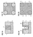
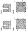
- Figures 1A, 2A , 3A and 4A depict cross sectional views of a structure during different process steps of a method according to a first embodiment of the invention.
- Figures 1B, 2B , 3B and 4B depict top views of the structure.
- Figures 1A and 1B show a plurality of structures in the form of cylindrical studs 1.
- the studs 1 are arranged on a substrate, more particularly on a hard mask layer 2 which in turn is deposited on a substrate.
- Hard mask layer 2 can be, e.g., formed of amorphous silicon. However, other materials can be used for forming layer 2.
- a skilled person acknowledges that there are different possible methods of forming studs 1.
- One possibility is a damascene process in silicon nitride, wherein the studs are formed of silicon oxide, for example.
- a damascene process in silicon nitride recesses in a silicon nitride layer are filled with a different material for forming the studs (e.g., silicon oxide as mentioned above).
- Figure 1A illustrates that studs 1 are formed in recesses of a silicon nitride layer 9.
- the silicon nitride is removed such that a plurality of spaced studs 1 are generated.
- other methods of fabricating a pattern of studs can be applied, e.g., direct structuring of a stud material layer.
- the studs 1 are arranged in a regular pattern on layer 2. More particularly, the studs are equally spaced in a pattern of several parallel columns and rows. In that respect a "column” or a “row” refers to a column or row of studs in which two neighboring studs have the smallest possible distance from each other. Referring to Figure 1B , for example, a column is formed by the studs which are arranged vertically and a row is formed by the horizontally arranged columns.
- the column and row like stud arrangement of the first embodiment is only exemplary and the invention comprises other stud layouts such as e.g. non-regular layouts or column-row layouts with different spaces between rows and columns or two or more different and alternating spaces between the columns and rows, respectively.
- a layer 3 (e.g., of aluminum oxide - Al 2 O 3 ) is deposited conformally such that the studs 1, more particularly sidewalls 11 of the studs 1 and a top portion of the studs, as well as a region between the studs 1 are covered by layer 3.
- the deposition of layer 3 can be performed by, e.g., chemical vapor deposition (CVD) or atomic layer deposition (ALD), e.g., followed by an annealing step.
- the layer is formed with a thickness of 0.1-0.3 F (F: minimal feature size).
- Layer 3 comprises a portion 31 which is located between the studs 1 and has a thickness (perpendicular to the substrate, i.e., to a surface of the hard mask layer 2) that is smaller than the height of the studs (measured from a surface of the hard mask layer 2 that faces the studs 1) such that studs 1 project above layer portion 31.
- the thickness of layer 3 exceeds the height of the studs.
- the layer portion 31 more specifically extends between sidewall portions 32 of layer 3 that cover the sidewalls 11 of the studs 1.
- the top portion of the studs 1 is covered by a top portion 33 of layer 3.
- the studs are created on layer 3, e.g., by depositing and structuring a stud layer on layer 3.
- the implantation comprises a first implantation step which is carried out under a first direction of incidence (first implant direction).
- the first implant direction is tilted, i.e., it runs inclined with respect to a direction perpendicular to the layer portion 31 (i.e., to a surface normal of layer portion 31).
- ions are used as implanting particles.
- other kinds of particles can be employed such as non-charged atoms or molecules.
- the first direction of incidence has an azimuthal component (x-y-component, i.e., the component that lies in a plane parallel to layer portion 31) which is not zero but runs diagonally with respect to the stud column.
- the first component runs with a first angle of approximately 45 degrees with respect to the stud columns.
- the first angle depends on a particular crystal orientation of layer 3, e.g., a main crystal axis.
- the distance between the middle of two neighboring implanted regions 312 (which extend diagonally with respect to the stud columns) is smaller than the distance between the center of two neighboring studs 1 of one column and row (which in Figure 1B extend vertically and horizontally), respectively.
- a further implantation step (third implantation step) is performed with an azimuthal component which is opposite to the azimuthal component of the first implantation direction, i.e., the azimuthal angle of the implant direction is rotated by 180°.
- the implant direction of the further implantation step has a component parallel to layer portion 31 running opposite to the first component of the first implantation direction, i.e., at an angle of 225 degrees with respect to the stud columns according to the first embodiment.
- the first and the further implantation step implant the same regions of layer portion 31. It is noted that the further implantation step is only optional.
- the implanted stripes 312 in layer portion 31 are removed (e.g., by cold or hot wet etching). Then, a second layer 4 (e.g., of aluminum oxide) is deposited, wherein layer 4 covers the remaining layer portion 31 in the non-implanted regions 313 (where layer portion 31 is not removed) such that a double layer is present on the hard mask layer 2, whereas only a single layer (layer 4) is present in the region of the removed implanted regions 312.
- a second layer 4 e.g., of aluminum oxide
- a second implantation step is performed with a second implantation direction (direction of incidence) which similarly to the first implantation step is inclined with respect to a direction perpendicular to layer portion 31 (tilted implantation).
- the second implantation direction has an azimuthal component that is essentially perpendicular to the azimuthal component of the first implantation direction, i.e., the second component has an angle of approximately 135 degrees with the stud columns according to the first embodiment.
- azimuthal component of the second implant direction does not necessarily have to run perpendicular to the azimuthal component of the first component.
- An embodiment of the invention comprises other angles than 90 degrees between these components.
- second implanted regions (not shown) arc formed in layer 4, wherein the second implanted regions extend longitudinally in the form of parallel stripes and perpendicular to the first implanted region 312 which were generated in layer portion 31.
- the second implanted regions thus cross the single layer region of layer 4 such that (rectangular) portions in the single layer region are implanted by the second implantation step.
- a further implantation step can be performed additionally to the second implantation step in order to increase the implantation dose in layer 4.
- additional implantation with an implantation direction is chosen that has an azimuthal component that extends opposite to the azimuthal component of the second direction of incidence, i.e., at an angle of 315 degrees with respect to the stud columns according to this embodiment.
- the further implantation is optional and can be carried out, e.g., after the second implantation step or at the same time with the second implantation step (e.g., by using two ion sources).
- the material of the second layer 4 is removed in the second implanted regions such that (rectangular) openings 315 are formed within the single layer region of the second layer 4.
- the openings 315 are arranged in a grid of parallel rows and columns which in the first embodiment is rotated by an angle of 45 degrees with respect to the stud columns and rows. In general, this angle depends on the twist of the first and second implantation direction with respect to the orientation of the stud columns.
- the use of aluminum oxide as the material of layer 3 and the second layer 4 is only exemplary.
- Other materials can be used in which a higher etchability relative to an etchant can be created by the implantation of ions.
- Examples of materials with an increased etch rate due to implantation are n-doped poly or amorphous silicon. See, e.g., "Doping and crystallographic effects in Cl-atom etching of silicon", Elmer A. Ogryzlo, Dale E. Ibbotson, Daniel L. Flamm, and John A. Mucha, AT&T Bell Laboratories, Murray Hill, New Jersey 07974.
- first and second layers 3, 4 can also be formed of a plurality of different layers or a separating layer can be deposited between the first and the second layer.
- heavy impactors such as Ar, Xe, Kr or F are used as implant species for the implantation of layer 3 and 4.
- other ions are also possible, e.g., hydrogen.
- the implantation is carried out with implant doses between 5E14 and 5E16 1/cm 2 .
- the applied dose is of course not restricted to that range but is chosen, e.g., dependent on the setup and the layer material.
- the figures only show a part of a structure (hard mask layer with studs) used in the manufacturing of a semiconductor device. Other parts of the semiconductor device might have the same pattern depicted here or might have different patterns. Furthermore, the patterns depicted above (and in the following embodiments). might be present in an intermediate state in the manufacturing of a semiconductor device or might be discernable in the final product.
- studs instead of studs, different means can be employed in order to shadow layer 3 or 4 with respect to the first and second implantation direction, respectively.
- an aperture which is separate to the substrate could be used.
- the geometry of the studs does not have to be cylindrical.
- Other stud geometries can be used such as asymmetric geometries, rectangular (not square) or elliptical.
- Figures 5A, 5B and 6A, 6B relate to a method in accordance with a second embodiment of the invention.
- a hard mask layer 2 is arranged on a substrate (not shown).
- a plurality of structures in the form of studs 1 is arranged, the studs 1 forming a regular column and row pattern on hard mask layer 2 similar to the first embodiment.
- a layer 3 of, e.g., amorphous silicon is deposited such that a portion 33 covers the top section of the studs 1, a portion 32 covers sidewalls of the studs 1 and a portion 31 extends between the studs 1 and thus covers a section of the hard mask layer 2.
- Layer portion 33 of layer 3 is removed from the studs 1 employing chemical mechanical polishing, CMP, wherein for stability reasons a sacrificial layer 5 is generated between the studs 1 as depicted in Figure 6A . After the top portions 33 are removed from the studs the sacrificial material 5 is stripped.
- CMP chemical mechanical polishing
- a first implantation step with a first direction of incidence is performed, wherein the first direction of incidence has an azimuthal component (parallel to layer 3) which runs at an angle of 45 degrees with respect to the stud columns. Therefore, the first implantation step creates stripe like first implanted regions 312 in layer 3 in a region that is not shadowed with respect to the first direction of incidence by the studs 1. Again an angle of 45 degrees is only exemplary, other angles are also possible.
- a second implantation step with a second direction of incidence is performed, wherein the second direction of incidence has an azimuthal component which runs at an angle of 135 degrees with respect to the stud columns, i.e., perpendicular to the first component of the first implant direction. Therefore, second strip like implanted regions 314 are created in layer 3 (more particularly, in the portion 31 of layer 3 extending between the studs 1) such that the second implanted regions 314 run at an angle of nearly 90 degrees with respect to the first implanted regions 312.
- both, the first and the second implanted regions 312, 314 extend with an angle of approximately 45 degrees with respect to columns in which the studs 1 are arranged. Located between neighboring studs, the first and second implanted regions 312 and 314 enclose a non-implanted region 313 which is neither implanted by the first implantation step nor implanted by the second implantation step.
- the non-implanted region 313 has a higher etchability with respect to an etchant compared to the implanted regions of layer 3.
- the non-implanted regions 313 are removed in order to uncover the hard mask layer 2, whereas the implanted regions 312, 314 are not removed.
- B or BF 2 ions are used as implant species with high doses (e.g., 5E14 - 5E16 1/cm 2 ) and the etching of the implanted regions is performed with NH 4 OH or KOH, e.g., in an aqueous solution in the concentration range from 60 parts water to 1 part NH4OH to 10 parts water to 1 part NH4OH or beyond.
- studs 1 are also removed using an appropriate etching step such that the hard mask layer 2 is uncovered also in the region of the studs.
- a grid of (essentially equally spaced) openings is thus created consisting of the openings in the region of the studs and in the regions of the non-implanted sections 313 of layer 3.
- the distance between two neighboring openings is half the distance of two neighboring studs of one stud column such that the generated grid of openings has only half the pitch as the studs 1 (i.e., the original structure) of the stud column.
- first and the second implantation direction (first and second direction of incidence) is inclined with respect to a surface normal of hard mask layer 2 such that the studs actually shadow a region of layer 3 with respect to the first and second implant direction.
- the inclination angle (implantation angle) is chosen dependent on the height of the studs such that a shadow with respect to the first and second implantation direction is created which extends from the structure to a neighboring structure.
- the first and the second implantation step can be completed by further implantation steps in order to enhance the implantation.
- ions are implanted with a (third) implant direction which has an azimuthal component which runs opposite with respect to the azimuthal component of the first implantation step.
- a (fourth) implantation step can be carried out enhancing the implantation of the second implantation step.
- Figures 7A, 7B and 8A, 8B relate to a problem which can occur if implanted regions of a first layer are removed and a second layer is deposited that is implanted in a second implantation step, as in the first embodiment.
- the shadowing structures studs
- Sidewalls 11 of the studs 1 are covered with a portion 32 of a layer 3 that is to be implanted.
- a first and a further implantation step in order to create a first implantation region 312 an upper portion 12 of the studs 1 is also implanted, whereas a lower portion 13 is not implanted such that the etchability of the upper portion is higher than the etchability of the lower portion 13.
- the first implanted regions 312 are removed the upper portion 12 (or at least a part of it) of the studs 1 is also removed which causes a deformation of the studs. This can lead to stud shadows with respect to the second implantation step with reduced accuracy.
- Figures 9A to 12B refer to another (third) embodiment of the invention which does not comprise a removal of implanted material after the first implantation step.
- Figures 9A, 10A , 11A and 12A illustrate side views and Figures 9B, 10B , 11B and 12B top views of the structure,
- a plurality of structures in the form of cylindrical studs 1 is formed on a hard mask layer 2. Similar to the first embodiment a layer 3 (e.g., of aluminum oxide) is deposited comprising a portion 31 which covers the hard mask layer 2 in a region between the studs 1. Another portion 32 of layer 3 covers sidewalls 11 of the studs 1.
- a layer 3 e.g., of aluminum oxide
- a first implantation is performed including a first implantation step at an angle of 45 degrees and a further (third) implantation step at an angle of 315 degrees (i.e., with an opposite azimuthal component) for enhancing the implantation as in the first embodiment.
- the (first) implantation direction of the first implantation step has an azimuthal component (i.e., parallel to the substrate and parallel to hard mask layer 2, respectively) which runs at an angle of 45 degrees with respect to columns in which the studs 1 are arranged.
- a second implantation is performed in turn including a second implantation step and an enhancing further implantation step, the second implantation step and the further implantation step having opposite azimuthal components.
- Figures 10A and 10B The result of the implantation is illustrated in Figures 10A and 10B , wherein Figure 10A illustrates the arrangement of Figure 10B viewed along the first implant direction (along a viewing direction V diagonal to the stud columns).
- First longitudinal implantation regions 312 (created by the first implantation) extend essentially parallel to one another and cross second implantation regions 314 (created by the second implantation) at an angle of about 90 degrees.
- the first and second implanted regions 312, 314 enclose a rectangular shaped non-implanted region 313.
- a top part 12 of the studs 1 is also implanted such that after removing the implanted regions 312, 314 also the top portion 12 of the sidewall section 32 of layer 3 is removed from studs 1 as depicted in Figure 11a .
- the implanted regions 312, 314 of layer 3 stripe-like openings 3120, 3140 are formed in layer 3 as illustrated in Figure 11B .
- the openings 3120, 3140 uncover a region of the underlying hard mask layer 2.
- the hard mask layer 2 is etched via the openings 3120, 3140 in order to form line-like structures 212, 214 in layer 2 permitting access to a layer (not shown) below the hard mask layer 2, e.g., a contact layer or active area regions of a device.
- a fourth embodiment of the invention is illustrated in Figures 13A to 16B .
- a regular pattern of studs 1 is produced on a hard mask layer 2.
- a layer 3 of material with an etchability (i.e., its etch rate) with respect to an etchant that is reduced upon implantation, e.g., aluminum oxide, is deposited.
- crosswise implantation is used in order to generate first and second line-like implantation regions 312, 314.
- the implanted regions 312, 314 enclose a non-implanted region 313 located in a region that was shadowed by the studs 1 both with respect to the first implant direction and the second implant direction.
- both the first and the second implanted regions 312, 314 are implanted twice from opposite directions (wherein the term "opposite direction” again refers to the azimuthal components).
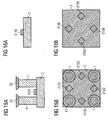
- the first and second implanted stripes 312, 314 overlap such that overlapping regions 315 are formed which were implanted four times (twice by a first implantation including a first implantation step and an enhancing further (third) implantation and twice by a second implantation including a second implantation step and a further (fourth) enhancing implantation step).
- a removal step is performed in order to only remove material of layer 3 outside of the overlapping regions 315. This can be done by using an etch process that removes the non-implanted and the double-implanted regions but does not remove the overlapping regions 315 which were implanted four times. For this, an etch step (e.g., dry etch) with a suited (linear or non-linear) contrast curve is applied. Examples of contrast curves of different etching means are given in Figures 24A, 24B and 25A, 25B .
- FIGs 15A and 15B The result of the removal step is shown in Figures 15A and 15B . Only the overlapping regions 315 were not removed such that pads 3150 on the underlying hard mask layer 2 are formed. Sidewall portions 32 of layer 3 covering the sidewalls of the studs 1 were equally removed during the removal step (see Figure 15A ), whereas the four times implanted top portions 33 of layer 3 are not removed. Therefore, in a subsequent etching step the studs 1 are removed, thereby lifting the top sections 33 of layer 3. The resulting final structure is shown in Figures 16A and 16B : Only the pads 3150 remain on the hard mask layer 2.
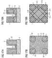
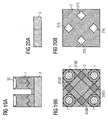
- FIG. 17A to 20B A fifth embodiment of the invention which also avoids the deposition of a second material layer is illustrated in Figures 17A to 20B .
- a plurality of cylindrical studs 1 is formed on hard mask layer 2 and a layer 3 is deposited, wherein the layer comprises a material whose etchability can be raised by implantation (e.g., aluminum oxide).
- the studs are arranged within essentially parallel columns and ions are implanted with a first implantation step at an angle of 45 and with a further implantation step 225 degrees with respect to the stud columns producing first implantation regions 312 within layer 3.
- layer 3 is implanted with a second implantation step at an angle of 13 5 and an additional implantation step at an angle of 315 degrees with respect to the stud columns such that second implanted regions 314 are produced that run perpendicular to the first implanted stripe-like regions 312.
- the first implanted regions 312 overlap with the second implanted regions 314 and thus overlapping regions 315 are formed, wherein the overlapping regions 315 have been implanted four times.
- an appropriate etching step e.g., wet etch
- an appropriate etching step only the four times implanted overlapping regions 315 are removed such that openings 3150 are created and the hard mask layer 2 is uncovered only within the overlapping regions 315.
- the region of layer outside the overlapping regions 315 i.e., regions of layer 3 which are not implanted or which are only implanted twice
- the etching step also removes top portion 33 of layer 3 which were covering the top of studs 1. This is shown in Figure 19A .
- the hard mask layer 2 is etched in the uncovered regions 315 such that openings 215 are generated in the hard mask layer 2 which in particular can be formed as through-openings to a layer below the hard mask layer 2 or the substrate.
- the resulting hard mask structure with reduced pitch is shown in Figure 20B .
- Figures 21A and 21B schematically illustrate the etching behavior (contrast curves) of etching means relative to a layer of amorphous silicon.
- amorphous silicon is only one example of a material whose etchability can be reduced by implantation.
- Other materials with a similar behavior are know to a skilled person.
- the material thickness that is removed by the etching means depends on the amount of implanted ions (BF 2 implant dose - x-axis, in relative units).
- Two different etching means wet only etchant (upper curve) and a combination of wet and dry etching (lower curve), are contemplated at first etching conditions (e.g., time of action, temperature). With respect to the wet only etchant, no etching occurs if the implant dose exceeds a certain dose (at approximately 380% in this schematic). If an implant dose below 100% is chosen the material layer is completely removed. As to the wet and dry etching curve, the layer is completely removed if the implant dose is below approximately 220%.
- combining a dry etch step with the wet etch enhances the contrast and may improve the etching, e.g., with respect to the fourth embodiment which requires non-implanted and twice implanted regions to be removed whereas four times implanted regions shall not be removed.
- the behavior of the etching means of Figure 21B at a second etching condition different from the first etching condition is illustrated in Figure 21B .
- the wet-only curve has a reduced slope compared to the wet only curve of the first etching condition ( Fig. 21A ).
- the behavior (the contrast curves) of the etching means illustrated in Figures 21A and 21B is only exemplary.
- Other etching means are available and can have different contrast curves, e.g., with an exponential characteristic.
- the schematic contrast curves shown in Figures 22A and 22B refer to etchant for etching an aluminum oxide layer.
- This material is only shown as an example of a material which can have a higher etchability in the implanted state.
- a first contrast curve for first etching conditions (labelled "conditions 2") are shown in Figure 22A . Below an offset an implant dose of about 150 percent no material is etched. Above 150% the etchabilty increases with a linear contrast curve.
- a linear contrast curve is only an example, other characteristics are possible.
- Figure 22B shows a contrast curve for the same etching means as in Figure 22A but under different etching conditions (labelled "conditions 2''').
- the contrast curve does not show any offset such that material is etched as soon as an amount of implanted ions is present.
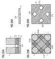
- FIG. 23A - 26B A method according to a sixth embodiment of the invention is illustrated in Figures 23A - 26B .
- a hard mask layer 2 is deposited on a substrate.
- an additional layer stack comprising further hard mask layers 6, 7 and 8 is generated over the hard mask layer 2, layer 7 being arranged between layer 6 and top layer 8. Shadowing structures in the form of studs 1 are generated on the top layer 8 of the layer stack.
- Layers 6 and 8 can be formed, e.g., of aluminum oxide, whereas layer 7 can be formed of, e.g., silicon oxide.
- the studs 1 can be formed of, e.g., carbon that, for example, is produced by an over-etch or an overexposure process (e.g., CD trim by lithography or by etching).
- top layer 8 extends in a region between the studs 1 and is partially implanted by a first implantation step using tilted ion implantation (as in the other embodiments) in order to produce first line-like implantation regions within portion 81.
- the material of layer 8 is removed in the first implanted regions such that layer 7 is uncovered which is subsequently removed by an etching step (e.g., dry etching).
- an etching step e.g., dry etching.
- FIGS 24A and 24B The situation after the etching of layer 7 is shown in Figures 24A and 24B . As illustrated in Figure 24A , recesses 712 are formed in layer 7 uncovering regions 612 of layer 6 which is located between hard mask layer 2 and layer 7.
- a second implantation is performed with an implant direction component parallel to the substrate (x-y-component) which is perpendicular to the x-y-component of the first implant direction such that second stripe-like implanted regions are formed that overlap with the uncovered regions 615 of layer 6 such that regions of layer 8 and rectangular regions 615 of layer 6 are implanted.
- the implanted material is removed, i.e., the second implanted regions 814 of layer 8 and the implanted region 615 of layer 6 are removed.
- openings 6150 are formed in layer 6 permitting the lower hard mask layer 2 to be etched in the region of the openings 6150 and form through opening in hard mask layer 2.
- the remaining layer 6, 7, 8 as well as studs 1 are be removed.
- only the hard mask layer 2 remains comprising a regular pattern of rectangularly formed openings 215. This is shown in Figures 26A and 26B .
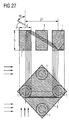
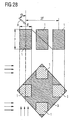
- Figure 27 illustrates the relationship between the height of circularly formed vertical studs 1 and the implantation angle ⁇ of an ion implantation step. Ions are radiated towards a layer 3 at the implantation angle ⁇ during implantation, i.e., the direction of incidence A runs inclined at the angle ⁇ with respect to a direction perpendicular to the layer 3 (the vertical direction in Figure 27 ).
- the angle ⁇ is chosen dependent on the height h of the structures such that a shadow created by one of the structures with respect to the implant direction extends from the structure to a next neighboring structure in the implant direction.
- the implantation direction A has a component which runs parallel to the layer 3 (i.e., parallel to the x-y-plane).
- a "next neighboring structure in the implant direction" of a structure is a structure that adjoins the structure along the direction of the x-y-component of the implant direction A (the horizontal, diagonal direction in Figure 27 ).
- the implant angle is limited to maximal 45 degrees, the minimal height of the studs is 2F for creating overlapping shadows. If the limit is 20 degrees the minimal height is 5.5F.
- other parameters can be taken into account for choosing the implant angle such as the aspect ratio of the studs, the critical dimensions of the studs, the final critical dimensions desired and the recoil behavior of the implant. Further, variations of the stud profile angles can be considered.
- the distance between two stud columns is 2F * 2 if the distance between neighboring studs is 2F.
- an integrated circuit is fabricated by performing first and second implantation steps, in either order.
- first implantation step particles are implanted into a layer under a first direction of incidence and, in the second implantation step, particles are implanted into the layer under a second direction of incidence that is different from the first direction of incidence.
- the layer which can have a thickness in the range of approximately 0.1 to approximately 0.3F as an example, is then partially removed depending on a local implant dose generated by the first and the second implantation step.
- the second direction of incidence is chosen to have an azimuthal component that runs obliquely relative to an azimuthal component of the first direction of incidence.
- the azimuthal component of the second direction of incidence can be perpendicular to the azimuthal component of the first direction of incidence.
- the first and the second direction of incidence both have a tilt angle with respect to the layer that is smaller than 45 degrees.
- first implanted regions can be created in the region of the layer that is not shadowed by the structures with respect to the first direction of incidence and second implanted regions can be created in the region of the layer that is not shadowed by the structures with respect to the second direction of incidence.
- first and/or the second implanted regions extend longitudinally, e.g., the first implanted regions run at an angle relative to the second implanted regions.
- the layer is removed within the overlapping regions so that openings are created within the overlapping regions.
- the layer comprising the openings can be used as a hard mask for structuring at least one further layer.
- the structures are arranged in a regular pattern, wherein in a cartesian pattern the structures are arranged in a plurality of essentially parallel columns and rows and wherein the azimuthal components of the first and the second direction of incidence run at an angle relative to the columns.
- the structures can be arranged in a cartesian or in a hexagonal pattern.
- neighboring structures cab have a center to center pitch of approximately 2F.
- the azimuthal components can run at an angle of approximately 45 degrees relative to the columns.
- the layer is deposited conformally such that the structures are also covered by the layer.
- the layer includes sidewall portions that each cover a sidewall of the structures.
- the thickness of the layer can be chosen dependent on the distance between neighboring structures such that projections of the sidewall portions of the neighboring structures do not overlap with respect to the first and/or second direction of incidence. For example, the layer can be removed from the structures before the first and the second implantation step.
- the layer comprises a material that has a lower etchabilty relative to an etchant in the implanted state than in the non-implanted state.
- the layer comprises at least one of a group comprising amorphous silicon, polysilicon and a polysilicon/SiON stack.
- the removal step can be performed using an etchant containing NH 4 OH or KOH and/or the implanted particles can be boron ions.
- Another embodiment of fabricating an integrated circuit includes performing a first implantation step, wherein particles are implanted into a first layer under a first direction of incidence and performing a first removal step, wherein the first layer is partially removed depending on a local implant dose generated by the first implantation step.
- a second implantation step can be performed to that particles are implanted into a second layer under a second direction of incidence and a second removal step can be performed so that the second layer is partially removed depending on the local implant dose generated by the second implantation step.
- the first implanted regions are created in a region of the first layer that is not shadowed by the structures with respect to the first direction of incidence and second implanted regions arc created in a region of the second layer that is not shadowed by the structures with respect to the second direction of incidence.
- the first removal step comprises removing the first implanted regions and/or the second removal step comprises removing the second implanted regions.
- an arrangement for generating an integrated circuit.
- a layer is disposed on a substrate and includes a plurality of first implanted regions and a plurality of second implanted regions that run at an angle relative to the first implanted regions.
- a plurality of structures can also be included, wherein the first and the second implanted regions extend between the structures.
- the structures can be arranged in a regular pattern.
- the structures can be columnarly shaped and/or have a circular or a rectangular cross section.
Landscapes
- Semiconductor Memories (AREA)
- Internal Circuitry In Semiconductor Integrated Circuit Devices (AREA)
- Element Separation (AREA)
Applications Claiming Priority (1)
| Application Number | Priority Date | Filing Date | Title |
|---|---|---|---|
| US11/855,809 US7825031B2 (en) | 2007-09-14 | 2007-09-14 | Method of fabricating a semiconductor device |
Publications (2)
| Publication Number | Publication Date |
|---|---|
| EP2037490A2 true EP2037490A2 (de) | 2009-03-18 |
| EP2037490A3 EP2037490A3 (de) | 2010-11-17 |
Family
ID=40081128
Family Applications (1)
| Application Number | Title | Priority Date | Filing Date |
|---|---|---|---|
| EP08015879A Withdrawn EP2037490A3 (de) | 2007-09-14 | 2008-09-09 | Verfahren zur Herstellung eines Halbleiterbauelements unter Verwendung von schrägen Implantaten |
Country Status (2)
| Country | Link |
|---|---|
| US (1) | US7825031B2 (de) |
| EP (1) | EP2037490A3 (de) |
Families Citing this family (1)
| Publication number | Priority date | Publication date | Assignee | Title |
|---|---|---|---|---|
| JP2012234057A (ja) * | 2011-05-02 | 2012-11-29 | Elpida Memory Inc | フォトマスクおよび半導体装置 |
Family Cites Families (7)
| Publication number | Priority date | Publication date | Assignee | Title |
|---|---|---|---|---|
| US5444007A (en) * | 1994-08-03 | 1995-08-22 | Kabushiki Kaisha Toshiba | Formation of trenches having different profiles |
| US6309975B1 (en) * | 1997-03-14 | 2001-10-30 | Micron Technology, Inc. | Methods of making implanted structures |
| FR2842944A1 (fr) * | 2002-07-23 | 2004-01-30 | St Microelectronics Sa | Procede de formation d'ouvertures de contact sur un circuit integre mos |
| DE10338503B3 (de) * | 2003-08-21 | 2005-05-25 | Infineon Technologies Ag | Herstellungsverfahren für eine Hartmaske für eine Halbleiterstruktur |
| US7172973B1 (en) * | 2004-11-02 | 2007-02-06 | National Semiconductor Corporation | System and method for selectively modifying a wet etch rate in a large area |
| JP4867171B2 (ja) * | 2005-01-21 | 2012-02-01 | 富士電機株式会社 | 半導体装置の製造方法 |
| US7179748B1 (en) * | 2005-08-02 | 2007-02-20 | Nanya Technology Corporation | Method for forming recesses |
-
2007
- 2007-09-14 US US11/855,809 patent/US7825031B2/en not_active Expired - Fee Related
-
2008
- 2008-09-09 EP EP08015879A patent/EP2037490A3/de not_active Withdrawn
Non-Patent Citations (1)
| Title |
|---|
| E.A. OGRYZLO, JOURNAL OF APPLIED PHYSICS, vol. 67, no. 6, 15 March 1990 (1990-03-15), pages 3115 - 3120 |
Also Published As
| Publication number | Publication date |
|---|---|
| US20090075462A1 (en) | 2009-03-19 |
| EP2037490A3 (de) | 2010-11-17 |
| US7825031B2 (en) | 2010-11-02 |
Similar Documents
| Publication | Publication Date | Title |
|---|---|---|
| US7429536B2 (en) | Methods for forming arrays of small, closely spaced features | |
| US10971368B2 (en) | Techniques for processing substrates using directional reactive ion etching | |
| US10777480B2 (en) | Systems and methods to enhance passivation integrity | |
| US10332748B2 (en) | Etch rate modulation through ion implantation | |
| CN107863318B (zh) | 基于间距倍增形成的集成电路图案及形成方法 | |
| CN102254915B (zh) | 具有掩埋位线的半导体器件及其制造方法 | |
| CN111279478B (zh) | 半导体装置结构及其制作方法 | |
| JP7648599B2 (ja) | 3d nandのための改質スタック | |
| EP2037490A2 (de) | Verfahren zur Herstellung eines Halbleiterbauelements unter Verwendung von schrägen Implantaten | |
| WO2009035798A1 (en) | Semiconductor constructions, semiconductor processing methods, and methods of forming flash memory structures | |
| US7553770B2 (en) | Reverse masking profile improvements in high aspect ratio etch | |
| US12387942B2 (en) | Modifying patterned features using a directional etch | |
| US20090045161A1 (en) | Integrated circuits, micromechanical devices, and method of making same | |
| CN117693192B (zh) | 半导体结构及其制备方法 | |
| US7557030B2 (en) | Method for fabricating a recess gate in a semiconductor device | |
| CN121510877A (zh) | 一种半导体结构的平坦化方法 | |
| CN118866818A (zh) | 用于形成半导体器件的方法和半导体器件 | |
| JP2008071951A (ja) | 半導体装置の製造方法 |
Legal Events
| Date | Code | Title | Description |
|---|---|---|---|
| PUAI | Public reference made under article 153(3) epc to a published international application that has entered the european phase |
Free format text: ORIGINAL CODE: 0009012 |
|
| AK | Designated contracting states |
Kind code of ref document: A2 Designated state(s): AT BE BG CH CY CZ DE DK EE ES FI FR GB GR HR HU IE IS IT LI LT LU LV MC MT NL NO PL PT RO SE SI SK TR |
|
| AX | Request for extension of the european patent |
Extension state: AL BA MK RS |
|
| 19U | Interruption of proceedings before grant |
Effective date: 20090401 |
|
| 19W | Proceedings resumed before grant after interruption of proceedings |
Effective date: 20091123 |
|
| PUAL | Search report despatched |
Free format text: ORIGINAL CODE: 0009013 |
|
| AK | Designated contracting states |
Kind code of ref document: A3 Designated state(s): AT BE BG CH CY CZ DE DK EE ES FI FR GB GR HR HU IE IS IT LI LT LU LV MC MT NL NO PL PT RO SE SI SK TR |
|
| AX | Request for extension of the european patent |
Extension state: AL BA MK RS |
|
| REG | Reference to a national code |
Ref country code: DE Ref legal event code: R108 |
|
| AKY | No designation fees paid | ||
| REG | Reference to a national code |
Ref country code: DE Ref legal event code: R108 Effective date: 20110714 |
|
| STAA | Information on the status of an ep patent application or granted ep patent |
Free format text: STATUS: THE APPLICATION IS DEEMED TO BE WITHDRAWN |
|
| 18D | Application deemed to be withdrawn |
Effective date: 20110416 |