EP2036071B1 - Bi-silicate matrix coating for a display - Google Patents
Bi-silicate matrix coating for a display Download PDFInfo
- Publication number
- EP2036071B1 EP2036071B1 EP06785299A EP06785299A EP2036071B1 EP 2036071 B1 EP2036071 B1 EP 2036071B1 EP 06785299 A EP06785299 A EP 06785299A EP 06785299 A EP06785299 A EP 06785299A EP 2036071 B1 EP2036071 B1 EP 2036071B1
- Authority
- EP
- European Patent Office
- Prior art keywords
- graphite
- matrix composition
- based matrix
- silicate
- sodium silicate
- Prior art date
- Legal status (The legal status is an assumption and is not a legal conclusion. Google has not performed a legal analysis and makes no representation as to the accuracy of the status listed.)
- Ceased
Links
- 239000011159 matrix material Substances 0.000 title claims description 58
- 239000011248 coating agent Substances 0.000 title description 18
- 238000000576 coating method Methods 0.000 title description 18
- OKTJSMMVPCPJKN-UHFFFAOYSA-N Carbon Chemical compound [C] OKTJSMMVPCPJKN-UHFFFAOYSA-N 0.000 claims description 53
- 229910002804 graphite Inorganic materials 0.000 claims description 53
- 239000010439 graphite Substances 0.000 claims description 53
- 239000000203 mixture Substances 0.000 claims description 37
- 239000004111 Potassium silicate Substances 0.000 claims description 23
- 239000004115 Sodium Silicate Substances 0.000 claims description 23
- 229910052913 potassium silicate Inorganic materials 0.000 claims description 23
- NNHHDJVEYQHLHG-UHFFFAOYSA-N potassium silicate Chemical compound [K+].[K+].[O-][Si]([O-])=O NNHHDJVEYQHLHG-UHFFFAOYSA-N 0.000 claims description 23
- 235000019353 potassium silicate Nutrition 0.000 claims description 23
- 229910052911 sodium silicate Inorganic materials 0.000 claims description 23
- NTHWMYGWWRZVTN-UHFFFAOYSA-N sodium silicate Chemical compound [Na+].[Na+].[O-][Si]([O-])=O NTHWMYGWWRZVTN-UHFFFAOYSA-N 0.000 claims description 23
- 239000011521 glass Substances 0.000 claims description 17
- XLYOFNOQVPJJNP-UHFFFAOYSA-N water Chemical compound O XLYOFNOQVPJJNP-UHFFFAOYSA-N 0.000 description 8
- 239000008367 deionised water Substances 0.000 description 5
- 229910021641 deionized water Inorganic materials 0.000 description 5
- 239000000853 adhesive Substances 0.000 description 4
- 230000001070 adhesive effect Effects 0.000 description 4
- 238000005054 agglomeration Methods 0.000 description 4
- 230000002776 aggregation Effects 0.000 description 4
- 239000000084 colloidal system Substances 0.000 description 4
- 239000006185 dispersion Substances 0.000 description 4
- RLQWHDODQVOVKU-UHFFFAOYSA-N tetrapotassium;silicate Chemical compound [K+].[K+].[K+].[K+].[O-][Si]([O-])([O-])[O-] RLQWHDODQVOVKU-UHFFFAOYSA-N 0.000 description 4
- 229910052910 alkali metal silicate Inorganic materials 0.000 description 3
- 239000000463 material Substances 0.000 description 3
- 238000000034 method Methods 0.000 description 3
- KRHYYFGTRYWZRS-UHFFFAOYSA-N Fluorane Chemical compound F KRHYYFGTRYWZRS-UHFFFAOYSA-N 0.000 description 2
- 125000006850 spacer group Chemical group 0.000 description 2
- OAICVXFJPJFONN-UHFFFAOYSA-N Phosphorus Chemical compound [P] OAICVXFJPJFONN-UHFFFAOYSA-N 0.000 description 1
- 230000015572 biosynthetic process Effects 0.000 description 1
- 239000003518 caustics Substances 0.000 description 1
- 238000000151 deposition Methods 0.000 description 1
- 238000005530 etching Methods 0.000 description 1
- 230000001678 irradiating effect Effects 0.000 description 1
- 238000004528 spin coating Methods 0.000 description 1
- 238000005406 washing Methods 0.000 description 1
Images


Classifications
-
- H—ELECTRICITY
- H01—ELECTRIC ELEMENTS
- H01J—ELECTRIC DISCHARGE TUBES OR DISCHARGE LAMPS
- H01J9/00—Apparatus or processes specially adapted for the manufacture, installation, removal, maintenance of electric discharge tubes, discharge lamps, or parts thereof; Recovery of material from discharge tubes or lamps
- H01J9/20—Manufacture of screens on or from which an image or pattern is formed, picked up, converted or stored; Applying coatings to the vessel
- H01J9/22—Applying luminescent coatings
- H01J9/227—Applying luminescent coatings with luminescent material discontinuously arranged, e.g. in dots or lines
- H01J9/2278—Application of light absorbing material, e.g. between the luminescent areas
-
- H—ELECTRICITY
- H01—ELECTRIC ELEMENTS
- H01J—ELECTRIC DISCHARGE TUBES OR DISCHARGE LAMPS
- H01J1/00—Details of electrodes, of magnetic control means, of screens, or of the mounting or spacing thereof, common to two or more basic types of discharge tubes or lamps
- H01J1/02—Main electrodes
- H01J1/30—Cold cathodes, e.g. field-emissive cathode
- H01J1/304—Field-emissive cathodes
-
- H—ELECTRICITY
- H01—ELECTRIC ELEMENTS
- H01J—ELECTRIC DISCHARGE TUBES OR DISCHARGE LAMPS
- H01J31/00—Cathode ray tubes; Electron beam tubes
- H01J31/08—Cathode ray tubes; Electron beam tubes having a screen on or from which an image or pattern is formed, picked up, converted, or stored
- H01J31/10—Image or pattern display tubes, i.e. having electrical input and optical output; Flying-spot tubes for scanning purposes
- H01J31/12—Image or pattern display tubes, i.e. having electrical input and optical output; Flying-spot tubes for scanning purposes with luminescent screen
- H01J31/123—Flat display tubes
- H01J31/125—Flat display tubes provided with control means permitting the electron beam to reach selected parts of the screen, e.g. digital selection
- H01J31/127—Flat display tubes provided with control means permitting the electron beam to reach selected parts of the screen, e.g. digital selection using large area or array sources, i.e. essentially a source for each pixel group
-
- H—ELECTRICITY
- H01—ELECTRIC ELEMENTS
- H01J—ELECTRIC DISCHARGE TUBES OR DISCHARGE LAMPS
- H01J9/00—Apparatus or processes specially adapted for the manufacture, installation, removal, maintenance of electric discharge tubes, discharge lamps, or parts thereof; Recovery of material from discharge tubes or lamps
- H01J9/02—Manufacture of electrodes or electrode systems
- H01J9/022—Manufacture of electrodes or electrode systems of cold cathodes
- H01J9/025—Manufacture of electrodes or electrode systems of cold cathodes of field emission cathodes
-
- H—ELECTRICITY
- H01—ELECTRIC ELEMENTS
- H01J—ELECTRIC DISCHARGE TUBES OR DISCHARGE LAMPS
- H01J2329/00—Electron emission display panels, e.g. field emission display panels
- H01J2329/18—Luminescent screens
- H01J2329/32—Means associated with discontinuous arrangements of the luminescent material
- H01J2329/323—Black matrix
Definitions
- This invention relates to a color display and, more particularly to a color display having phosphor deposits on a faceplate panel.
- color displays such as, for example, color cathode-ray tubes (CRTs) and field emission devices (FEDs) typically include display screens.
- the display screens are formed from glass plates coated with an array of three different color-emitting phosphors.
- a graphite-based matrix is placed in the interstitial regions between each of the three different color-emitting phosphors.
- any of US 2003/0230966 A1 and US 2004/0058613 A1 discloses a display comprising a glass display screen having a patterned light-absorbing matrix composition thereon defining a pluraltiy of sets of fields.
- graphite-based matrix compositions lose adherence to glass and exhibits weak internal strength when physical contact is made thereto.
- spacers are placed in contact with the graphite-based matrix composition. Because of the weakness of the graphite matrix coating, adhesive failure may occur primarily at the coating/glass interface, such that the spacers may fall over. Adhesive failure may also occur within the body of the graphite-based matrix composition causing it to come away from the display screen.
- the present invention relates to a display screen of a color display.
- the display screen includes a glass plate having an array of three different color-emitting phosphors thereon.
- a graphite-based matrix is placed in the interstitial regions between each of the three different color-emitting phosphors.
- the graphite-based matrix is formed from an aqueous composition including graphite, potassium silicate and sodium silicate.
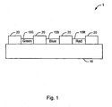
- FIG. 1 shows a side view of a portion of a display screen 1 of a color display.
- the display screen 1 includes a glass plate 10 having an array of three different color-emitting phosphors 15G, 15B, 15R thereon.
- a graphite-based matrix 20 is placed in the interstitial regions between each of the three different color-emitting phosphors 15G, 15B, 15R.
- the exemplary display screen 1 described herein may be a faceplate panel for a color cathode-ray tube (CRT) as well as a field emission display (FEDs), among other display screens.
- CTR color cathode-ray tube
- FEDs field emission display
- the graphite-based matrix is formed from an aqueous composition including graphite, potassium silicate and sodium silicate.
- a mixed alkali silicate imparts adhesive strength to the graphite-based matrix composition in a two-fold manner.
- Potassium silicate hardens at room temperature and provides the graphite-based matrix composition with enough strength to survive subsequent processing steps.
- Sodium silicate hardens during baking (e.g., at 450 °C) so there is good adherence at the coating/glass interface and within the body of the coating during subsequent processing steps.
- sodium silicate is the only alkali silicate in the graphite-based matrix composition
- the graphite-based matrix composition washes off the glass during subsequent processing steps.
- potassium silicate is the only alkali silicate in the graphite-based matrix composition, the graphite-based matrix composition does not have enough adhesive strength to survive subsequent processing steps.
- the potassium silicate and sodium silicate may be present in the aqueous composition in a ratio of about 1:1 to about 5:1 sodium silicate to potassium silicate. Further, the aqueous composition should preferably include up to 10 % by weight sodium silicate and potassium silicate.
- An exemplary aqueous graphite-based matrix solution is formed by mixing 14.4 grams of Kasil 2135 potassium silicate (commercially available from PQ Corporation, Valley Forge, PA), 9.4 grams of J sodium silicate (commercially available from PQ Corporation, Valley Forge, PA), 100 grams Electrodag 1530 graphite dispersion (commercially available from Acheson Colloids Company, Port Huron, MI) and in 128.9 grams of deionized water.
- the aqueous graphite-based matrix solution is further mixed on a jar roller for more than about 30 minutes. After mixing the graphite-based matrix composition should be applied to a display screen within about 24 hours to avoid agglomeration.
- a coating formed from the graphite-based matrix composition of Example 1 was tested for adhesion. No failure occurred at the glass/coating interface or within the body of the coating.
- An exemplary aqueous graphite-based matrix solution is formed by mixing 8.1 grams of Kasil 2135 potassium silicate (commercially available from PQ Corporation, Valley Forge, PA), 5.25 grams of J sodium silicate (commercially available from PQ Corporation, Valley Forge, PA), 100 grams Electrodag 1530 graphite dispersion (commercially available from Acheson Colloids Company, Port Huron, MI) and in 83.75 grams of deionized water.
- the aqueous graphite-based matrix solution is further mixed on a jar roller for more than about 30 minutes. After mixing the graphite-based matrix composition should be applied to a display screen within about 24 hours to avoid agglomeration.
- a coating formed from the graphite-based matrix composition of Example 2 was tested for adhesion. No failure occurred at the glass/coating interface or within the body of the coating.
- An exemplary aqueous graphite-based matrix solution is formed by mixing 5.84 grams of Kasil 2135 potassium silicate (commercially available from PQ Corporation, Valley Forge, PA), 11.98 grams of J sodium silicate (commercially available from PQ Corporation, Valley Forge, PA), 100 grams Electrodag 1530 graphite dispersion (commercially available from Acheson Colloids Company, Port Huron, MI) and in 111.31 grams of deionized water.
- the aqueous graphite-based matrix solution is further mixed on a jar roller for more than about 30 minutes. After mixing the graphite-based matrix composition should be applied to a display screen within about 24 hours to avoid agglomeration.
- a coating formed from the graphite-based matrix composition of Example 3 was tested for adhesion. No failure occurred at the glass/coating interface or within the body of the coating.
- An exemplary aqueous graphite-based matrix solution is formed by mixing 3.9 grams of Kasil 2135 potassium silicate (commercially available from PQ Corporation, Valley Forge, PA), 12.6 grams of J sodium silicate (commercially available from PQ Corporation, Valley Forge, PA), 100 grams Electrodag 1530 graphite dispersion (commercially available from Acheson Colloids Company, Port Huron, MI) and in 112.0 grams of deionized water.
- the aqueous graphite-based matrix solution is further mixed on a jar roller for more than about 30 minutes. After mixing the graphite-based matrix composition should be applied to a display screen within about 24 hours to avoid agglomeration.
- a coating formed from the graphite-based matrix composition of Example 4 was tested for adhesion. No failure occurred at the glass/coating interface or within the body of the coating.
- the method for forming the graphite-based matrix of the present invention on the display screen of the color display will be described.
- the interior surface of the display screen 10 is cleaned, as indicated by reference numeral 100 in FIG. 2 and FIG. 3A , by washing it with a caustic solution, rinsing it in water, etching it with buffered hydrofluoric acid and rinsing it again with water, as is known in the art.
- the interior surface of the display screen 10 is then provided with the graphite-based matrix 20, as indicated by reference numeral 102.
- the graphite-based matrix 20 is uniformly applied over the interior surface of the display screen 10 using for example, a spin coating technique, as is known in the art.
- the graphite-based matrix preferably has a thickness of about 0.0762 mm (0.003 inches) to about 0.254 mm (0.010 inches).
- the display screen 10 is baked to about 450 °C for about 40 minutes to remove the water therefrom.
- the graphite-based matrix 20 is patterned, as indicated by reference numeral 106 in FIG. 2 , to form openings therein within which three different color-emitting phosphors 15G, 15B, 15R ( FIG.1 ) are deposited.
- the graphite-based matrix 20 is patterned by depositing a light sensitive material 25 thereon and irradiating portions of such layer to light, such as for example, ultraviolet (UV) light.
- the light sensitive material 25 is developed using, for example, deionized water. During development, portions of the light sensitive material 25 are removed. Thereafter, as shown in FIG. 3D , portions of the graphite-based matrix 20 are removed in regions where the three different color-emitting phosphors 15G, 15B, 15R are to be subsequently deposited.
- the above-described graphite-based matrix composition has improved adherence to the glass of the color display screen.
- the graphite-based matrix composition has improved coating strength.
Landscapes
- Engineering & Computer Science (AREA)
- Manufacturing & Machinery (AREA)
- Cathode-Ray Tubes And Fluorescent Screens For Display (AREA)
- Carbon And Carbon Compounds (AREA)
Description
- This invention relates to a color display and, more particularly to a color display having phosphor deposits on a faceplate panel.
- Many color displays, such as, for example, color cathode-ray tubes (CRTs) and field emission devices (FEDs) typically include display screens. The display screens are formed from glass plates coated with an array of three different color-emitting phosphors. To provide contrast, a graphite-based matrix is placed in the interstitial regions between each of the three different color-emitting phosphors.
- Any of
US 2003/0230966 A1 andUS 2004/0058613 A1 discloses a display comprising a glass display screen having a patterned light-absorbing matrix composition thereon defining a pluraltiy of sets of fields. - Many graphite-based matrix compositions lose adherence to glass and exhibits weak internal strength when physical contact is made thereto. During assembly of filed emission devices, spacers are placed in contact with the graphite-based matrix composition. Because of the weakness of the graphite matrix coating, adhesive failure may occur primarily at the coating/glass interface, such that the spacers may fall over. Adhesive failure may also occur within the body of the graphite-based matrix composition causing it to come away from the display screen.
- Thus, a need exists for a graphite-based matrix composition with improved adhesion to a glass display screen.
- The present invention relates to a display screen of a color display. The display screen includes a glass plate having an array of three different color-emitting phosphors thereon. A graphite-based matrix is placed in the interstitial regions between each of the three different color-emitting phosphors. The graphite-based matrix is formed from an aqueous composition including graphite, potassium silicate and sodium silicate.
- A preferred implementation of the principles of the present invention will now be described in greater detail, with relation to the accompanying drawings, in which:
-
FIG. 1 is a side view of a portion of a display screen of a color display including a graphite-based matrix of the present invention; -
FIG. 2 is flow chart of the process for forming the graphite-based matrix of the present invention on the display screen of the color display; and -
FIGS. 3A-3D depict views of the interior surface of the faceplate panel during formation of the luminescent screen assembly. -
FIG. 1 shows a side view of a portion of adisplay screen 1 of a color display. Thedisplay screen 1 includes aglass plate 10 having an array of three different color-emittingphosphors matrix 20 is placed in the interstitial regions between each of the three different color-emittingphosphors exemplary display screen 1 described herein may be a faceplate panel for a color cathode-ray tube (CRT) as well as a field emission display (FEDs), among other display screens. - The graphite-based matrix is formed from an aqueous composition including graphite, potassium silicate and sodium silicate. The addition of a mixed alkali silicate imparts adhesive strength to the graphite-based matrix composition in a two-fold manner. Potassium silicate hardens at room temperature and provides the graphite-based matrix composition with enough strength to survive subsequent processing steps. Sodium silicate hardens during baking (e.g., at 450 °C) so there is good adherence at the coating/glass interface and within the body of the coating during subsequent processing steps. When sodium silicate is the only alkali silicate in the graphite-based matrix composition, the graphite-based matrix composition washes off the glass during subsequent processing steps. When potassium silicate is the only alkali silicate in the graphite-based matrix composition, the graphite-based matrix composition does not have enough adhesive strength to survive subsequent processing steps.
- The potassium silicate and sodium silicate may be present in the aqueous composition in a ratio of about 1:1 to about 5:1 sodium silicate to potassium silicate. Further, the aqueous composition should preferably include up to 10 % by weight sodium silicate and potassium silicate.
- An exemplary aqueous graphite-based matrix solution is formed by mixing 14.4 grams of Kasil 2135 potassium silicate (commercially available from PQ Corporation, Valley Forge, PA), 9.4 grams of J sodium silicate (commercially available from PQ Corporation, Valley Forge, PA), 100 grams Electrodag 1530 graphite dispersion (commercially available from Acheson Colloids Company, Port Huron, MI) and in 128.9 grams of deionized water. The aqueous graphite-based matrix solution is further mixed on a jar roller for more than about 30 minutes. After mixing the graphite-based matrix composition should be applied to a display screen within about 24 hours to avoid agglomeration.
- A coating formed from the graphite-based matrix composition of Example 1 was tested for adhesion. No failure occurred at the glass/coating interface or within the body of the coating.
- An exemplary aqueous graphite-based matrix solution is formed by mixing 8.1 grams of Kasil 2135 potassium silicate (commercially available from PQ Corporation, Valley Forge, PA), 5.25 grams of J sodium silicate (commercially available from PQ Corporation, Valley Forge, PA), 100 grams Electrodag 1530 graphite dispersion (commercially available from Acheson Colloids Company, Port Huron, MI) and in 83.75 grams of deionized water. The aqueous graphite-based matrix solution is further mixed on a jar roller for more than about 30 minutes. After mixing the graphite-based matrix composition should be applied to a display screen within about 24 hours to avoid agglomeration.
- A coating formed from the graphite-based matrix composition of Example 2 was tested for adhesion. No failure occurred at the glass/coating interface or within the body of the coating.
- An exemplary aqueous graphite-based matrix solution is formed by mixing 5.84 grams of Kasil 2135 potassium silicate (commercially available from PQ Corporation, Valley Forge, PA), 11.98 grams of J sodium silicate (commercially available from PQ Corporation, Valley Forge, PA), 100 grams Electrodag 1530 graphite dispersion (commercially available from Acheson Colloids Company, Port Huron, MI) and in 111.31 grams of deionized water. The aqueous graphite-based matrix solution is further mixed on a jar roller for more than about 30 minutes. After mixing the graphite-based matrix composition should be applied to a display screen within about 24 hours to avoid agglomeration.
- A coating formed from the graphite-based matrix composition of Example 3 was tested for adhesion. No failure occurred at the glass/coating interface or within the body of the coating.
- An exemplary aqueous graphite-based matrix solution is formed by mixing 3.9 grams of Kasil 2135 potassium silicate (commercially available from PQ Corporation, Valley Forge, PA), 12.6 grams of J sodium silicate (commercially available from PQ Corporation, Valley Forge, PA), 100 grams Electrodag 1530 graphite dispersion (commercially available from Acheson Colloids Company, Port Huron, MI) and in 112.0 grams of deionized water. The aqueous graphite-based matrix solution is further mixed on a jar roller for more than about 30 minutes. After mixing the graphite-based matrix composition should be applied to a display screen within about 24 hours to avoid agglomeration.
- A coating formed from the graphite-based matrix composition of Example 4 was tested for adhesion. No failure occurred at the glass/coating interface or within the body of the coating.
- Referring to
FIG. 2 andFIGS. 3A-3D , the method for forming the graphite-based matrix of the present invention on the display screen of the color display will be described. Initially, the interior surface of thedisplay screen 10 is cleaned, as indicated byreference numeral 100 inFIG. 2 andFIG. 3A , by washing it with a caustic solution, rinsing it in water, etching it with buffered hydrofluoric acid and rinsing it again with water, as is known in the art. - As shown in
FIG. 3B , the interior surface of thedisplay screen 10 is then provided with the graphite-basedmatrix 20, as indicated byreference numeral 102. The graphite-basedmatrix 20 is uniformly applied over the interior surface of thedisplay screen 10 using for example, a spin coating technique, as is known in the art. The graphite-based matrix preferably has a thickness of about 0.0762 mm (0.003 inches) to about 0.254 mm (0.010 inches). As indicated byreference numeral 104 inFIG. 2 , after the graphite-based matrix is applied to thedisplay screen 10, thedisplay screen 10 is baked to about 450 °C for about 40 minutes to remove the water therefrom. - The graphite-based
matrix 20 is patterned, as indicated byreference numeral 106 inFIG. 2 , to form openings therein within which three different color-emittingphosphors FIG.1 ) are deposited. Referring toFIG. 3C , the graphite-basedmatrix 20 is patterned by depositing a light sensitive material 25 thereon and irradiating portions of such layer to light, such as for example, ultraviolet (UV) light.
The light sensitive material 25 is developed using, for example, deionized water. During development, portions of the light sensitive material 25 are removed. Thereafter, as shown inFIG. 3D , portions of the graphite-basedmatrix 20 are removed in regions where the three different color-emittingphosphors - The above-described graphite-based matrix composition has improved adherence to the glass of the color display screen. In addition, the graphite-based matrix composition has improved coating strength.
- Although an exemplary color display screen for a color cathode-ray tube (CRT) or field emission device (FED) which incorporates the teachings of the present invention has been shown and described in detail herein, those skilled in the art can readily devise many other varied embodiments that still incorporate these teachings.
Claims (9)
- A display, comprising: a glass display screen (10) having a patterned light-absorbing matrix composition (20) thereon defining a plurality of sets of fields, characterized in that the light-absorbing matrix composition includes graphite, potassium silicate and sodium silicate.
- The display of claim 1 characterized in that the potassium silicate and sodium silicate are present in the light-absorbing matrix composition (20) in a ratio of 1 :1 to 5:1 sodium silicate:potassium silicate.
- The display of claim 1 characterized in that the light-absorbing matrix composition (20) includes less than 10 % by weight of potassium silicate and sodium silicate.
- A cathode-ray tube, comprising: a glass display screen (10) having a patterned light-absorbing matrix composition (20) thereon defining a plurality of sets of fields, characterized in that the light-absorbing matrix composition includes graphite, potassium silicate and sodium silicate.
- The cathode-ray tube of claim 4 characterized in that the potassium silicate and sodium silicate are present in the light-absorbing matrix composition (20) in a ratio of 1 :1 to 5: 1 sodium silicate:potassium silicate.
- The cathode-ray tube of claim 4 characterized in that the light-absorbing matrix composition (20) includes less than 10 % by weight of potassium silicate and sodium silicate.
- A field emission device, comprising: a glass display screen (10) having a patterned light-absorbing matrix composition (20) thereon defining a plurality of sets of fields, characterized in that the light-absorbing matrix composition (20) includes graphite, potassium silicate and sodium silicate.
- The field emission device of claim 7 characterized in that the potassium silicate and sodium silicate are present in the light-absorbing matrix composition (20) in a ratio of 1 : 1 to 5: 1 sodium silicate:potassium silicate.
- The field emission device of claim 7 characterized in that the light-absorbing matrix composition (20) includes less than 10 % by weight of potassium silicate and sodium silicate.
Applications Claiming Priority (1)
| Application Number | Priority Date | Filing Date | Title |
|---|---|---|---|
| PCT/US2006/024220 WO2007149084A1 (en) | 2006-06-21 | 2006-06-21 | Bi-silicate matrix coating for a display |
Publications (3)
| Publication Number | Publication Date |
|---|---|
| EP2036071A1 EP2036071A1 (en) | 2009-03-18 |
| EP2036071A4 EP2036071A4 (en) | 2009-07-08 |
| EP2036071B1 true EP2036071B1 (en) | 2010-08-04 |
Family
ID=38833708
Family Applications (1)
| Application Number | Title | Priority Date | Filing Date |
|---|---|---|---|
| EP06785299A Ceased EP2036071B1 (en) | 2006-06-21 | 2006-06-21 | Bi-silicate matrix coating for a display |
Country Status (7)
| Country | Link |
|---|---|
| US (1) | US8138664B2 (en) |
| EP (1) | EP2036071B1 (en) |
| JP (1) | JP2009541931A (en) |
| KR (1) | KR101213607B1 (en) |
| CN (1) | CN101473364A (en) |
| DE (1) | DE602006016022D1 (en) |
| WO (1) | WO2007149084A1 (en) |
Family Cites Families (16)
| Publication number | Priority date | Publication date | Assignee | Title |
|---|---|---|---|---|
| JPS515856B2 (en) * | 1972-07-26 | 1976-02-23 | ||
| US3998638A (en) * | 1975-05-22 | 1976-12-21 | Westinghouse Electric Corporation | Method of developing opaquely coated sensitized matrix with a solution containing sodium meta-silicate |
| US4188564A (en) * | 1976-12-13 | 1980-02-12 | U.S. Philips Corporation | Cathode ray tube having low resistance contact area beneath high voltage contact spring |
| NL7907596A (en) * | 1979-10-15 | 1981-04-21 | Philips Nv | COLOR TELEVISION PICTURE TUBE. |
| NL8102200A (en) * | 1981-05-06 | 1982-12-01 | Philips Nv | COLOR IMAGE TUBE. |
| JP2731539B2 (en) * | 1988-08-08 | 1998-03-25 | 鹿児島日本電気株式会社 | Fluorescent display tube |
| JPH0271963U (en) * | 1988-11-22 | 1990-05-31 | ||
| JPH0448530A (en) * | 1990-06-15 | 1992-02-18 | Mitsubishi Electric Corp | Color cathode ray tube and its manufacture |
| US6117294A (en) * | 1996-01-19 | 2000-09-12 | Micron Technology, Inc. | Black matrix material and methods related thereto |
| US6554671B1 (en) * | 1997-05-14 | 2003-04-29 | Micron Technology, Inc. | Method of anodically bonding elements for flat panel displays |
| US5885669A (en) * | 1997-08-08 | 1999-03-23 | Acheson Industries, Inc. | Liquid crystal device and method |
| DE60028281T2 (en) * | 1999-03-23 | 2007-05-24 | Ngk Insulators, Ltd., Nagoya | Process for producing a beryllium-copper body bonded by hot isostatic pressing and the body connected by hot isostatic pressing |
| JP2001283750A (en) * | 2000-04-04 | 2001-10-12 | Futaba Corp | Anode substrate for light emitting device and method of manufacturing the same |
| CN100407362C (en) * | 2002-04-12 | 2008-07-30 | 三星Sdi株式会社 | field emission display |
| JP3439469B1 (en) * | 2002-06-13 | 2003-08-25 | 株式会社 カクマ | Fluorescent film of electron beam tube and display device using electron beam tube using the same |
| WO2008002287A2 (en) * | 2006-06-23 | 2008-01-03 | Thomson Licensing | Black matrix coating for a display |
-
2006
- 2006-06-21 WO PCT/US2006/024220 patent/WO2007149084A1/en not_active Ceased
- 2006-06-21 DE DE602006016022T patent/DE602006016022D1/en not_active Expired - Lifetime
- 2006-06-21 US US12/308,590 patent/US8138664B2/en active Active
- 2006-06-21 JP JP2009516464A patent/JP2009541931A/en active Pending
- 2006-06-21 KR KR1020087030837A patent/KR101213607B1/en not_active Expired - Fee Related
- 2006-06-21 CN CNA2006800550397A patent/CN101473364A/en active Pending
- 2006-06-21 EP EP06785299A patent/EP2036071B1/en not_active Ceased
Also Published As
| Publication number | Publication date |
|---|---|
| DE602006016022D1 (en) | 2010-09-16 |
| KR20090023393A (en) | 2009-03-04 |
| US8138664B2 (en) | 2012-03-20 |
| EP2036071A1 (en) | 2009-03-18 |
| CN101473364A (en) | 2009-07-01 |
| JP2009541931A (en) | 2009-11-26 |
| US20100231117A1 (en) | 2010-09-16 |
| WO2007149084A1 (en) | 2007-12-27 |
| EP2036071A4 (en) | 2009-07-08 |
| KR101213607B1 (en) | 2012-12-18 |
Similar Documents
| Publication | Publication Date | Title |
|---|---|---|
| US8138664B2 (en) | Bi-silicate matrix coating for a display | |
| US20090251042A1 (en) | Black Matrix Coating for a Display | |
| US20090026952A1 (en) | Phosphor paste and plasma display panel using the same | |
| US7994695B2 (en) | Luminescent materials for a carbon nanotube (CNT) field emission device (FED) | |
| KR20010062296A (en) | Electrode plate and manufacturing method for the same, and gas discharge panel having electrode plate and manufacturing method for the same | |
| US20080238298A1 (en) | Image display device | |
| KR20090023387A (en) | Black Matrix Coatings for Displays | |
| MXPA05008197A (en) | Method of manufacturing a color filter cathode ray tube (crt). | |
| JP3506720B2 (en) | Gas discharge display | |
| JP2002083551A (en) | Back substrate of plasma display panel and method of manufacturing the same, and plasma display panel and method of manufacturing the same | |
| JP2002338959A (en) | Phosphor particles and method for producing the same, display panel and method for producing the same, and flat display device and method for producing the same | |
| CN100356501C (en) | rear panel of plasma display panel | |
| KR100315222B1 (en) | A manufacturing method of anode for a flat display panel and the flat display panel having the anode | |
| Kim et al. | 32.2: Development of PDP Rear Panel by Etching Technology | |
| JP2000234087A (en) | Phosphor, method for surface treatment of phosphor, and method for forming phosphor layer | |
| KR100986893B1 (en) | Field emission device manufacturing method | |
| US20080297049A1 (en) | Plasma display panel and method for fabricating the same | |
| KR100429835B1 (en) | Manufacturing method of field emission device | |
| JP2001236021A (en) | Display panel | |
| US20110217453A1 (en) | Manufacturing method of substrate having function layer between partition walls, and manufacturing method of image display apparatus using the substrate | |
| JP2001210236A (en) | Method of forming phosphor layer | |
| JPH09165230A (en) | Fine-grained frit glass coating method and image display device using fine-grained frit glass | |
| US20080231163A1 (en) | Plasma display panel and method for manufacturing the same | |
| JP2002117769A (en) | Gas discharge type display device and manufacturing method thereof | |
| KR20090084106A (en) | Phosphor composition and method for manufacturing phosphor layer of plasma display panel using same |
Legal Events
| Date | Code | Title | Description |
|---|---|---|---|
| PUAI | Public reference made under article 153(3) epc to a published international application that has entered the european phase |
Free format text: ORIGINAL CODE: 0009012 |
|
| 17P | Request for examination filed |
Effective date: 20081230 |
|
| AK | Designated contracting states |
Kind code of ref document: A1 Designated state(s): AT BE BG CH CY CZ DE DK EE ES FI FR GB GR HU IE IS IT LI LT LU LV MC NL PL PT RO SE SI SK TR |
|
| AX | Request for extension of the european patent |
Extension state: AL BA HR MK RS |
|
| A4 | Supplementary search report drawn up and despatched |
Effective date: 20090605 |
|
| RIC1 | Information provided on ipc code assigned before grant |
Ipc: H01J 9/227 20060101ALI20090529BHEP Ipc: H01J 29/32 20060101AFI20090529BHEP Ipc: H01J 1/72 20060101ALI20090529BHEP |
|
| DAX | Request for extension of the european patent (deleted) | ||
| RBV | Designated contracting states (corrected) |
Designated state(s): DE FR GB |
|
| GRAP | Despatch of communication of intention to grant a patent |
Free format text: ORIGINAL CODE: EPIDOSNIGR1 |
|
| RAP1 | Party data changed (applicant data changed or rights of an application transferred) |
Owner name: THOMSON LICENSING |
|
| GRAS | Grant fee paid |
Free format text: ORIGINAL CODE: EPIDOSNIGR3 |
|
| GRAA | (expected) grant |
Free format text: ORIGINAL CODE: 0009210 |
|
| AK | Designated contracting states |
Kind code of ref document: B1 Designated state(s): DE FR GB |
|
| REG | Reference to a national code |
Ref country code: GB Ref legal event code: FG4D |
|
| REF | Corresponds to: |
Ref document number: 602006016022 Country of ref document: DE Date of ref document: 20100916 Kind code of ref document: P |
|
| PLBE | No opposition filed within time limit |
Free format text: ORIGINAL CODE: 0009261 |
|
| STAA | Information on the status of an ep patent application or granted ep patent |
Free format text: STATUS: NO OPPOSITION FILED WITHIN TIME LIMIT |
|
| 26N | No opposition filed |
Effective date: 20110506 |
|
| REG | Reference to a national code |
Ref country code: DE Ref legal event code: R097 Ref document number: 602006016022 Country of ref document: DE Effective date: 20110506 |
|
| REG | Reference to a national code |
Ref country code: FR Ref legal event code: PLFP Year of fee payment: 11 |
|
| REG | Reference to a national code |
Ref country code: FR Ref legal event code: PLFP Year of fee payment: 12 |
|
| REG | Reference to a national code |
Ref country code: FR Ref legal event code: PLFP Year of fee payment: 13 |
|
| REG | Reference to a national code |
Ref country code: FR Ref legal event code: TP Owner name: THOMSON LICENSING DTV, FR Effective date: 20180830 |
|
| REG | Reference to a national code |
Ref country code: GB Ref legal event code: 732E Free format text: REGISTERED BETWEEN 20180927 AND 20181005 |
|
| REG | Reference to a national code |
Ref country code: DE Ref legal event code: R082 Ref document number: 602006016022 Country of ref document: DE Representative=s name: DEHNS, DE Ref country code: DE Ref legal event code: R081 Ref document number: 602006016022 Country of ref document: DE Owner name: INTERDIGITAL MADISON PATENT HOLDINGS, FR Free format text: FORMER OWNER: THOMSON LICENSING, ISSY-LES-MOULINEAUX, FR Ref country code: DE Ref legal event code: R082 Ref document number: 602006016022 Country of ref document: DE Representative=s name: DEHNS PATENT AND TRADEMARK ATTORNEYS, DE |
|
| P01 | Opt-out of the competence of the unified patent court (upc) registered |
Effective date: 20230514 |
|
| PGFP | Annual fee paid to national office [announced via postgrant information from national office to epo] |
Ref country code: DE Payment date: 20230627 Year of fee payment: 18 Ref country code: FR Payment date: 20230622 Year of fee payment: 18 |
|
| PGFP | Annual fee paid to national office [announced via postgrant information from national office to epo] |
Ref country code: GB Payment date: 20230620 Year of fee payment: 18 |
|
| REG | Reference to a national code |
Ref country code: DE Ref legal event code: R119 Ref document number: 602006016022 Country of ref document: DE |
|
| GBPC | Gb: european patent ceased through non-payment of renewal fee |
Effective date: 20240621 |
|
| PG25 | Lapsed in a contracting state [announced via postgrant information from national office to epo] |
Ref country code: DE Free format text: LAPSE BECAUSE OF NON-PAYMENT OF DUE FEES Effective date: 20250101 |
|
| PG25 | Lapsed in a contracting state [announced via postgrant information from national office to epo] |
Ref country code: FR Free format text: LAPSE BECAUSE OF NON-PAYMENT OF DUE FEES Effective date: 20240630 |
|
| PG25 | Lapsed in a contracting state [announced via postgrant information from national office to epo] |
Ref country code: GB Free format text: LAPSE BECAUSE OF NON-PAYMENT OF DUE FEES Effective date: 20240621 |