EP2034528A1 - Electronic component - Google Patents
Electronic component Download PDFInfo
- Publication number
- EP2034528A1 EP2034528A1 EP07744305A EP07744305A EP2034528A1 EP 2034528 A1 EP2034528 A1 EP 2034528A1 EP 07744305 A EP07744305 A EP 07744305A EP 07744305 A EP07744305 A EP 07744305A EP 2034528 A1 EP2034528 A1 EP 2034528A1
- Authority
- EP
- European Patent Office
- Prior art keywords
- electronic component
- electrode
- electrodes
- circuit board
- side end
- Prior art date
- Legal status (The legal status is an assumption and is not a legal conclusion. Google has not performed a legal analysis and makes no representation as to the accuracy of the status listed.)
- Withdrawn
Links
Images





Classifications
-
- H—ELECTRICITY
- H10—SEMICONDUCTOR DEVICES; ELECTRIC SOLID-STATE DEVICES NOT OTHERWISE PROVIDED FOR
- H10H—INORGANIC LIGHT-EMITTING SEMICONDUCTOR DEVICES HAVING POTENTIAL BARRIERS
- H10H20/00—Individual inorganic light-emitting semiconductor devices having potential barriers, e.g. light-emitting diodes [LED]
- H10H20/80—Constructional details
- H10H20/85—Packages
- H10H20/858—Means for heat extraction or cooling
- H10H20/8582—Means for heat extraction or cooling characterised by their shape
-
- H—ELECTRICITY
- H10—SEMICONDUCTOR DEVICES; ELECTRIC SOLID-STATE DEVICES NOT OTHERWISE PROVIDED FOR
- H10H—INORGANIC LIGHT-EMITTING SEMICONDUCTOR DEVICES HAVING POTENTIAL BARRIERS
- H10H20/00—Individual inorganic light-emitting semiconductor devices having potential barriers, e.g. light-emitting diodes [LED]
- H10H20/80—Constructional details
- H10H20/85—Packages
- H10H20/8506—Containers
-
- H—ELECTRICITY
- H10—SEMICONDUCTOR DEVICES; ELECTRIC SOLID-STATE DEVICES NOT OTHERWISE PROVIDED FOR
- H10H—INORGANIC LIGHT-EMITTING SEMICONDUCTOR DEVICES HAVING POTENTIAL BARRIERS
- H10H20/00—Individual inorganic light-emitting semiconductor devices having potential barriers, e.g. light-emitting diodes [LED]
- H10H20/80—Constructional details
- H10H20/85—Packages
- H10H20/858—Means for heat extraction or cooling
- H10H20/8585—Means for heat extraction or cooling being an interconnection
-
- H—ELECTRICITY
- H10—SEMICONDUCTOR DEVICES; ELECTRIC SOLID-STATE DEVICES NOT OTHERWISE PROVIDED FOR
- H10W—GENERIC PACKAGES, INTERCONNECTIONS, CONNECTORS OR OTHER CONSTRUCTIONAL DETAILS OF DEVICES COVERED BY CLASS H10
- H10W72/00—Interconnections or connectors in packages
- H10W72/01—Manufacture or treatment
- H10W72/0198—Manufacture or treatment batch processes
-
- H—ELECTRICITY
- H10—SEMICONDUCTOR DEVICES; ELECTRIC SOLID-STATE DEVICES NOT OTHERWISE PROVIDED FOR
- H10W—GENERIC PACKAGES, INTERCONNECTIONS, CONNECTORS OR OTHER CONSTRUCTIONAL DETAILS OF DEVICES COVERED BY CLASS H10
- H10W72/00—Interconnections or connectors in packages
- H10W72/50—Bond wires
- H10W72/541—Dispositions of bond wires
- H10W72/547—Dispositions of multiple bond wires
- H10W72/5473—Dispositions of multiple bond wires multiple bond wires connected to a common bond pad
-
- H—ELECTRICITY
- H10—SEMICONDUCTOR DEVICES; ELECTRIC SOLID-STATE DEVICES NOT OTHERWISE PROVIDED FOR
- H10W—GENERIC PACKAGES, INTERCONNECTIONS, CONNECTORS OR OTHER CONSTRUCTIONAL DETAILS OF DEVICES COVERED BY CLASS H10
- H10W72/00—Interconnections or connectors in packages
- H10W72/50—Bond wires
- H10W72/551—Materials of bond wires
- H10W72/552—Materials of bond wires comprising metals or metalloids, e.g. silver
- H10W72/5522—Materials of bond wires comprising metals or metalloids, e.g. silver comprising gold [Au]
-
- H—ELECTRICITY
- H10—SEMICONDUCTOR DEVICES; ELECTRIC SOLID-STATE DEVICES NOT OTHERWISE PROVIDED FOR
- H10W—GENERIC PACKAGES, INTERCONNECTIONS, CONNECTORS OR OTHER CONSTRUCTIONAL DETAILS OF DEVICES COVERED BY CLASS H10
- H10W72/00—Interconnections or connectors in packages
- H10W72/50—Bond wires
- H10W72/551—Materials of bond wires
- H10W72/552—Materials of bond wires comprising metals or metalloids, e.g. silver
- H10W72/5524—Materials of bond wires comprising metals or metalloids, e.g. silver comprising aluminium [Al]
-
- H—ELECTRICITY
- H10—SEMICONDUCTOR DEVICES; ELECTRIC SOLID-STATE DEVICES NOT OTHERWISE PROVIDED FOR
- H10W—GENERIC PACKAGES, INTERCONNECTIONS, CONNECTORS OR OTHER CONSTRUCTIONAL DETAILS OF DEVICES COVERED BY CLASS H10
- H10W72/00—Interconnections or connectors in packages
- H10W72/851—Dispositions of multiple connectors or interconnections
- H10W72/874—On different surfaces
- H10W72/884—Die-attach connectors and bond wires
-
- H—ELECTRICITY
- H10—SEMICONDUCTOR DEVICES; ELECTRIC SOLID-STATE DEVICES NOT OTHERWISE PROVIDED FOR
- H10W—GENERIC PACKAGES, INTERCONNECTIONS, CONNECTORS OR OTHER CONSTRUCTIONAL DETAILS OF DEVICES COVERED BY CLASS H10
- H10W74/00—Encapsulations, e.g. protective coatings
-
- H—ELECTRICITY
- H10—SEMICONDUCTOR DEVICES; ELECTRIC SOLID-STATE DEVICES NOT OTHERWISE PROVIDED FOR
- H10W—GENERIC PACKAGES, INTERCONNECTIONS, CONNECTORS OR OTHER CONSTRUCTIONAL DETAILS OF DEVICES COVERED BY CLASS H10
- H10W76/00—Containers; Fillings or auxiliary members therefor; Seals
- H10W76/40—Fillings or auxiliary members in containers, e.g. centering rings
- H10W76/42—Fillings
- H10W76/47—Solid or gel fillings
-
- H—ELECTRICITY
- H10—SEMICONDUCTOR DEVICES; ELECTRIC SOLID-STATE DEVICES NOT OTHERWISE PROVIDED FOR
- H10W—GENERIC PACKAGES, INTERCONNECTIONS, CONNECTORS OR OTHER CONSTRUCTIONAL DETAILS OF DEVICES COVERED BY CLASS H10
- H10W90/00—Package configurations
-
- H—ELECTRICITY
- H10—SEMICONDUCTOR DEVICES; ELECTRIC SOLID-STATE DEVICES NOT OTHERWISE PROVIDED FOR
- H10W—GENERIC PACKAGES, INTERCONNECTIONS, CONNECTORS OR OTHER CONSTRUCTIONAL DETAILS OF DEVICES COVERED BY CLASS H10
- H10W90/00—Package configurations
- H10W90/701—Package configurations characterised by the relative positions of pads or connectors relative to package parts
- H10W90/731—Package configurations characterised by the relative positions of pads or connectors relative to package parts of die-attach connectors
- H10W90/734—Package configurations characterised by the relative positions of pads or connectors relative to package parts of die-attach connectors between a chip and a stacked insulating package substrate, interposer or RDL
-
- H—ELECTRICITY
- H10—SEMICONDUCTOR DEVICES; ELECTRIC SOLID-STATE DEVICES NOT OTHERWISE PROVIDED FOR
- H10W—GENERIC PACKAGES, INTERCONNECTIONS, CONNECTORS OR OTHER CONSTRUCTIONAL DETAILS OF DEVICES COVERED BY CLASS H10
- H10W90/00—Package configurations
- H10W90/701—Package configurations characterised by the relative positions of pads or connectors relative to package parts
- H10W90/751—Package configurations characterised by the relative positions of pads or connectors relative to package parts of bond wires
- H10W90/754—Package configurations characterised by the relative positions of pads or connectors relative to package parts of bond wires between a chip and a stacked insulating package substrate, interposer or RDL
Definitions
- the present invention relates to an electronic component having a frame fixed on the upper surface of a circuit board, and more specifically to an electronic component suitable for a surface-mounted LED used as a light source for switch internal illumination, an LED display, a backlight light source, an optical printer head, a camera flash, or the like.
- the depression is arranged near the first and second side ends, upon mounting the electronic component by soldering the lower electrode, solder easily penetrate into the depression, thus permitting improvement in operability in soldering.
- the terminal sections of the electrodes 16 and 17 for wiring are fixed to terminal sections of a different circuit board with a conducting material such as solder.
- the electrode 15 for heat radiation is also fixed to a terminal section or a heat sink section of a different circuit board with a conducting material such as solder.
- the frame 3 is formed of a material having excellent heat conductivity, and aluminum is used in this embodiment, but magnesium or any other metal material can also be used. Moreover, instead of a metal material, a member having a resin surface or a ceramic surface coated with a metal material, a member having a plurality of metal materials or ceramic materials coupled together with an adhesive material such as resin or metal, a member having metal dispersed in resin, or the like can also be used. Moreover, the frame 3 may be composed of resin only.
- a plurality of LED elements 7 are provided, and thus light-emitting diodes for three primary colors, i.e., red, green, and blue can be used. Instead of these, light-emitting diodes for two colors or a light-emitting diode for a single color may be used, or light emitting diodes for four or more colors can also be used.
- the LED elements 7 have a plurality of colors and they emit light simultaneously, the different colors are mixed together and extracted to the outside through the transmissive resin 11.
- FIGS. 5(1) to (9 ) are flow diagrams showing representative processes of manufacturing the surface-mounted LED 1.
- structure of the circuit board 2 and the frame 3 are partially omitted and thus simply expressed.
- an aluminum thin plate 26 is supplied.
- the thickness of the aluminum thin plate 26 is selected from among ranges 0.5 mm to 2 mm or 0.5 mm to 3 mm.
- the coating material 23 is filled in the grooves 28 formed in the third process.
- an insulating material such as resist is used as the coating material 23.
- the frame aggregate 27 and the circuit board aggregate 29 are fixed with the expected cut lines in line.
- the fixation of the frame aggregate 27 and the circuit board aggregate 29 is performed with the insulating adhesive 25.
- the fixation may be done by using a conductive jointing material such as a conductive adhesive or solder, or other fixing means may be used.
- the LED elements 7 are loaded on the circuit board aggregate 29 and wiring of the thin metal wires 8 and 9 are performed through wire bonding.
- the surface-mounted LED 1 as the electronic component shown in FIGS. 1 and 4 described above is manufactured.
- the surface-mounted LED is formed with an upper surface thereof sized several millimeters square and with a thickness of approximately 0.3 mm to 3 mm.
- Four side surfaces of this surface-mounted LED 1 is cut simultaneously with the dicing saw 30; therefore, the circuit board 2 and the frame 3 fixed thereto have four side surfaces 41 (common side surfaces) composed of the same surface.
- the electrode 15 for heat radiation formed on the lower surface of the surface-mounted LED 1 extends from the central part of the lower surface to its both side ends, occupying a wide area. Specifically, the electrode 15 for heat radiation is formed over a range from, of an opposing pair of side ends 20A and 20B on the lower surface of the circuit board 2, one side end 20A (first side end) to the other side end 20B (second side end).
- a group of depressions 18 collected in a comb-like form along a planar shape of the through hole 13 is arranged.
- a group of depressions 18 collected in the form of fish bone is arranged.
- the frame 3 includes around the opening 10 a circumference surface widening upward. Light emitted from the LED element 7 is reflected by the circumference surface of the frame 3. Therefore, the circumference surface of the frame 3 functions as a reflective surface, and can improve the light use efficiency.
- FIG. 9 is a top view showing a surface-mounted LED 1 as an electronic component of the third embodiment.
- FIG. 10 is a bottom view showing the surface-mounted LED 1.
- FIG. 11 is a bottom view showing a state of FIG. 10 with coating 19 (hatched portion) omitted.
- portions the same as those in the first embodiment shown in FIGS. 1 to 4 described above are provided with the same numerals.
- Ground electrodes 31 and 32 (see FIGS. 6 and 7 ) the same as those of the second embodiment may be provided, and terminal sections of the electrodes 16 and 17 may be provided at the side end 20D as is the case with the third embodiment.
- the typical film thickness of alumite is approximately 20 ⁇ m, but can be thickened to approximately 100 ⁇ m.
- the use of thick-filmed alumite as the coating material 23 can improve effect of insulation and effect of preventing metal burr.
- the invention can be used for an electronic component having a frame fixed on the upper surface of a circuit board. More specifically, the invention is applicable to a surface-mounted LED used as a light source for switch inner illumination, an LED display, a backlight light source, an optical printer head, a camera flash, or the like.
Landscapes
- Led Device Packages (AREA)
Abstract
Description
- The present invention relates to an electronic component having a frame fixed on the upper surface of a circuit board, and more specifically to an electronic component suitable for a surface-mounted LED used as a light source for switch internal illumination, an LED display, a backlight light source, an optical printer head, a camera flash, or the like.
-
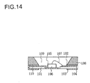
Patent Document 1 discloses a surface-mounted LED as a conventional electronic component.FIG. 14 is a sectional view showing this surface-mounted LED. The surface-mounted LED haselectrodes 102 and 103 provided on the upper surface side and lower surface side of aninsulating substrate 101. Theelectrodes 102 and 103 are connected to each other by athrough hole 104. Below an opening of theinsulating substrate 101, anelectrode 105 is provided, which is mounted with anLED element 106 with a conducting material. The front side electrode of theLED element 106 and theelectrode 102 are connected together with athin metal wire 107. - On the circumference portion of the surface-mounted LED, a
reflective frame 108 as a frame is provided. Thereflective frame 108 is typically formed of an insulating material as a resin material, and is fixed on theelectrodes reflective frame 108,transmissive resin 109 is filled. This encapsulates theLED element 106 and thethin metal wire 107. - Moreover, a surface-mounted LED is known which has the
reflective frame 108 formed of a metal member for heat radiation. This surface-mounted LED has an insulating film provided on the surfaces of 102 and 105 for the purpose of preventing short circuit of polar electrodes. - [Patent Document 1]
JP-A-H7-235696 FIG. 8 ) - The electronic component of this type has an
electrode 105 provided below an opening of aninsulating substrate 101 and equipped with anLED element 106 with a conducting material, so that heat generated by theLED element 106 is radiated via theelectrode 105. However, theelectrode 105 has low degree of freedom in arrangement, which has raised a problem that sufficient heat radiation effect cannot be provided. - It is an object of the invention to provide an electronic component that can improve heat radiation performance.
- To solve the problem described above, the present invention refers to an electronic component including a circuit board having a plurality of electrodes on upper and lower surface of an insulating substrate and a thermogenic circuit element fixed to an upper surface of the circuit board. The electronic component further includes: an upper electrode on which the circuit element is placed; a through hole penetrating through the insulating substrate; and a lower electrode formed on a lower surface side in a range from a first side end of the circuit board to a second side end thereof opposing the first side end, the lower electrode being connected to the upper electrode via the through hole.
- With this configuration, the upper electrode is formed on the upper surface of the insulating substrate forming the circuit board, and the lower electrode connected to the upper electrode via the through hole is formed on the lower surface of the insulating substrate. The lower electrode is formed over an opposing pair of first and second side ends. The circuit element is placed on the upper electrode, and heat generated by the circuit element is radiated via the upper electrode and the lower electrode.
- Preferrably, in the electronic component with the configuration described above, the upper electrode and the lower electrode are adapted to be electrically nonpolar.
- Preferrably, in the electronic component with the configuration described above, terminal sections of a plurality of polar electrodes are arranged along opposing third and fourth side ends extending in a direction crossing the first and second side ends. With this configuration, the polar electrodes are disposed at both side parts of the lower electrode formed over the first and second side ends, and a voltage is applied to the circuit element via the terminal sections of the polar electrodes.
- Preferrably, in the electronic component with the configuration described above, the lower electrode has a wider area than each of the polar electrodes.
- Preferrably, in the electronic component with the configuration described above, the terminal sections of the polar electrodes are arranged along the third side end extending in the direction crossing the first and second side ends, and the lower electrode is provided in a manner such as to extend to the fourth side end opposing the third side end. With this configuration, the polar electrodes are disposed at one side part of the lower electrode formed over the first and second side ends, and a voltage is applied to the circuit element via the terminal sections of the polar electrodes.
- Preferrably, in the electronic component with the configuration described above, the upper electrode and the lower electrode are grounded.
- Preferrably, in the electronic component with the configuration described above, a depression in a shape along the through hole is formed on a surface of the lower electrode.
- Preferrably, in the electronic component with the configuration described above, a joint surface between the upper electrode and the lower electrode is composed of an upper surface of the through hole.
- Preferrably, in the electronic component with the configuration described above, the depression is arranged near the first and second side ends.
- Preferrably, in the electronic component with the configuration described above, a frame enclosing the surrounding of the circuit element and composed of a good heat conductor is provided in contact with the upper electrode.
- Preferrably, in the electronic component with the configuration described above, the circuit element is composed of an LED element, and emitted light of the LED element is reflected by the frame.
- According to the present invention, since a lower electrode connected via a through hole to an upper electrode on which a circuit element is placed is formed over opposing first and second side ends of a circuit board, a wide area of the lower electrode can be ensured. As a result, heat generated by the circuit element can be efficiently radiated via the upper electrode and the lower electrode, which permits improvement in the heat radiation performance of an electronic component.
- According to the present invention, since the upper electrode and the lower electrode are adapted to be electrically nonpolar, the degree of freedom in arrangement for the upper electrode and the lower electrode can be made higher than for the polar electrodes. Therefore, the electronic component with high heat radiation performance can easily be achieved.
- According to the invention, since terminal sections of a plurality of polar electrodes are arranged along opposing third and fourth side ends extending in a direction crossing the first and second side ends, an electronic component can easily be achieved which supplies power to the circuit element via the terminal sections of the polar electrodes and which has high heat radiation performance. Moreover, since the polar electrodes and the lower electrode are arranged in distinction from each other, wiring to the terminal sections of the polar electrodes can easily be performed. Therefore, operability in assembling a device loaded with the electronic component can be improved.
- According to the invention, since the lower electrode has a wider area than each of the polar electrodes, the heat radiation performance of the electronic component can be improved.
- According to the invention, since the terminal sections of the polar electrodes are arranged along the third side end extending in the direction crossing the first and second side ends and the lower electrode is provided in a manner such as to extend to the fourth side end opposing the third side end, the area of the lower electrode can be made even larger. Therefore, the heat radiation performance of the electronic component can be further improved.
- According to the invention, since the upper electrode and the lower electrode are grounded, one terminal of the circuit element can be connected to the upper electrode having a wide area. Therefore, operability in assembling the electronic component can be improved.
- According to the invention, since a depression in a shape along the through hole is formed on a surface of the lower electrode, the heat radiation area can be more increased to further improve the heat radiation performance. Moreover, upon mounting the electronic component by soldering the lower electrode, the solder joint area can be increased to improve joint strength. Further, since solder is embedded in the depressions during soldering, the metal volume increases, which enlarges a heat conduction path, resulting in smooth heat radiation, which permits further improvement in the heat radiation performance.
- According to the invention, since a joint surface between the upper electrode and the lower electrode is composed of an upper surface of the through hole, the depression can easily be formed by forming the lower electrode on an insulating substrate formed with the through hole.
- According to the invention, since the depression is arranged near the first and second side ends, upon mounting the electronic component by soldering the lower electrode, solder easily penetrate into the depression, thus permitting improvement in operability in soldering.
- According to the invention, since a frame enclosing the surrounding of the circuit element and composed of a good heat conductor is provided in contact with the upper electrode, heat generated from the circuit element is radiated via the frame. Therefore, the heat radiation performance of the electronic component can be further improved.
-
- [
FIG. 1 ] is a perspective sectional view showing an electronic component of a first embodiment of the present invention. - [
FIG. 2 ] is a top view showing the electronic component of the first embodiment of the invention. - [
FIG. 3 ] is a bottom view showing the electronic component of the first embodiment of the invention. - [
FIG. 4 ] is a bottom view of the electronic component of the first embodiment of the invention with coating omitted. - [
FIG. 5 ] is a process diagram showing one example of a method for manufacturing the electronic component of the first embodiment of the invention. - [
FIG. 6 ] is a top view showing an electronic component of a second embodiment of the invention. - [
FIG. 7 ] is a bottom view showing the electronic component of the second embodiment of the invention. - [
FIG. 8 ] is a bottom view of the electronic component of the second embodiment of the invention with coating omitted. - [
FIG. 9 ] is a top view showing an electronic component of a third embodiment of the invention. - [
FIG. 10 ] is a bottom view showing the electronic component of the third embodiment of the invention. - [
FIG. 11 ] is a bottom view of the electronic component of the third embodiment of the invention with coating omitted. - [
FIG. 12 ] is a perspective sectional view showing an electronic component of a fourth embodiment of the invention. - [
FIG. 13 ] is a perspective sectional view showing an electronic component of a fifth embodiment of the invention. - [
FIG. 14 ] is a sectional view showing a conventional electronic component. -
- 1 Surface-mounted LED
- 2 Circuit board
- 3 Frame
- 4 Electrode (nonpolar)
- 5, 6 Electrodes (polar)
- 7, 106 LED elements
- 8, 9, 107 Thin metal wires
- 10 opening
- 11 Transmissive resin
- 12 Insulating substrate
- 13, 14 Through holes
- 15 Electrode (for heat radiation)
- 16, 17 Electrodes (for wiring)
- 18 Depression
- 19 Coating
- 20 Side surface
- 21 Cut surface
- 22 Empty space
- 23 Coating material
- 24 Insulating layer
- 25 Adhesive
- 26 Aluminum thin plate
- 27 Frame aggregate
- 28 Groove
- 29 Board aggregate
- 30 Dicing saw
- 31, 32 Ground electrodes
- 41 Side surface
- Hereinafter, the embodiments of the present invention will be described with reference to the accompanying drawings.
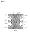
FIG. 1 is a perspective sectional view showing a surface-mounted LED (light-emitting diode) 1 as an electronic component of a first embodiment.FIG. 2 is a top view showing a state of the surface-mountedLED 1 withtransmissive resin 11 omitted.FIG. 3 is a bottom view showing the surface-mountedLED 1.FIG. 4 is a bottom view showing a state ofFIG. 3 with coating 19 (hatched portions) omitted. - The surface-mounted
LED 1 is structured to have aframe 3 fixed on the upper surface of acircuit board 2. Theframe 3 has anopening 10 vertically penetrating therethrough, and is disposed on the circumference portion of thecircuit board 2. In theopening 10, a nonpolar electrode 4 (upper electrode) andpolar electrodes electrodes substrate 12 of thecircuit board 2. Theelectrode 5 has either of positive and negative polarities, while theelectrode 6 has the other polarity. Theelectrode 5 haselectrodes LED elements 7 to be described later. Theelectrode 6 haselectrodes LED elements 7. Theelectrode 4 is electrically separated from theelectrodes - The plurality of electrodes 5 (5R, 5G, and 5B) and 6 (6R, 6G, and 6B) respectively having positive and negative polarities are arranged on the upper surface of the
circuit board 2 inside theopening 10 of theframe 3. Thenonpolar electrode 4 is arranged in a region other than theelectrodes opening 10 of theframe 3, and is also arranged between the lower surface of theframe 3 and thecircuit board 2. That is, theelectrode 4 is formed to extend over a wide range in such a manner as to cover almost the entire upper surface of thecircuit board 2 excluding theelectrodes - On the
nonpolar electrode 4, anLED element 7 as a circuit element is loaded. One electrode of theLED element 7 is connected to thepolar electrode 5 with athin metal wire 8. The other electrode of theLED element 7 is connected to thepolar electrode 6 with athin metal wire 9. Theopening 10 is filled withtransmissive resin 11, which encapsulates theLED element 7 and thethin metal wires - In the insulating
substrate 12 of thecircuit board 2, a throughhole 13 is provided below theelectrode 4, and throughholes 14 are provided below theelectrodes substrate 12,electrodes electrode 16 haselectrodes LED elements 7. Theelectrode 17 haselectrodes LED elements 7. - The electrode 15 (lower electrode) is connected to the
electrode 4 via the throughhole 13. Theelectrodes 5R, RG, and 5B and theelectrodes hole 14. Moreover, theelectrodes electrodes hole 14. -
FIG. 4 shows by cross-hatching the electrodes 16 (16R, 16G, and 16B) and 17 (17R, 17G, and 17B) connected to thepolar electrodes electrode 15 connected to thenonpolar electrode 4. The electrodes 16 (16R, 16G, and 16B) and 17 (17R, 17G, and 17B) connected to thepolar electrodes electrode 15 connected to thenonpolar electrode 4 is mainly for heat radiation and functions as a nonpolar electrode. - On the
electrode 15 for heat radiation, adepression 18 is formed on which a planar shape of the throughhole 13 provided in the insulatingsubstrate 12 is reflected. The throughhole 13 is formed by microfabrication through laser processing after theelectrode 4 is provided on the insulatingsubstrate 12. Thereafter, theelectrode 15 is formed on the lower surface of the insulatingsubstrate 12, whereby theelectrodes hole 13, thereby forming thedepression 18 in the shape along the throughhole 13. With thedepression 18, a geometric pattern is formed on the rear surface of thecircuit board 2. - The width of the
depression 18 can be formed in the size of 0.1 mm to 0.5 mm by forming the throughhole 13 by the microfabrication through laser processing. Therefore, forming the geometric pattern on metal by machining such as drilling makes it difficult to make the width narrower than approximately 0.5 mm, but the width of thedepression 18 can be formed narrowly by laser processing. - For the insulating
substrate 12, liquid crystal polymer, insulating resin, glass epoxy, ceramic, or the like can be used. The use of the liquid crystal polymer for the insulatingsubstrate 12 is preferable since it is suitable for microfabricatioin. The thickness of the insulatingsubstrate 12 can be selected from a range between 0.01 mm and 0.1mm, considering strength, insulation performance and heat radiation performance. Setting the thickness of the insulatingsubstrate 12 at, for example, 0.025 mm is preferable since it can maintain strength, insulation performance, and heat radiation performance high. - The
electrode 15 for heat radiation is directly connected to thenonpolar electrode 4 via a large number of throughholes 13, thus permitting heat generated at theLED elements 7 to be efficiently radiated via theelectrode 15 for heat radiation. Since this promotes heat radiation of theLED elements 7, deterioration in light emission efficiency due to temperature increase of theLED elements 7 decreases, permitting providing high brightness proportional to the amount of current. Therefore, effect of improving the functionality of the surface-mountedLED 1 and improving the life can be provided. - The
electrodes FIG. 3 , coated with the insulatingcoating 19. Theelectrode 15 for heat radiation can be partially coated with the insulatingcoating 19, but, for the purpose of increasing heat radiation performance, is all exposed without being coated with the insulatingcoating 19. - The terminal sections of the
electrodes electrode 15 for heat radiation is also fixed to a terminal section or a heat sink section of a different circuit board with a conducting material such as solder. - The
frame 3 is formed of a material having excellent heat conductivity, and aluminum is used in this embodiment, but magnesium or any other metal material can also be used. Moreover, instead of a metal material, a member having a resin surface or a ceramic surface coated with a metal material, a member having a plurality of metal materials or ceramic materials coupled together with an adhesive material such as resin or metal, a member having metal dispersed in resin, or the like can also be used. Moreover, theframe 3 may be composed of resin only. - The
side surface 41 of the surface-mountedLED 1 on the side on which the terminal sections of theelectrodes FIG. 1 , composed of the same surface as theside surface 20 of theframe 3, and at the lower section of theframe 3,empty spaces 22 are formed which is composed of grooves. Theempty space 22 is formed by acut surface 21 over theside surface 20 and the lower surface of theframe 3. Theempty space 22 formed by thecut surface 21 is shaped into a quarter-circle in cross section, but may be shaped into a different shape such as a triangle or a rectangle in cross section as long as the insulating distance can be maintained. - In the
empty space 22 formed by thecut surface 21 at a corner portion over theside surface 20 and the lower surface of theframe 3, acoating material 23 is filled. Thecoating material 23 is composed of an insulating material, but as later described in the other embodiment, may be composed of a conducting material when thecoating material 23 is formed on thecut surface 21 in a predetermined thickness without filling theempty space 22. Moreover, thecut surface 21 may be exposed without being coated. - The
frame 3 is fixed to thecircuit board 2 with an adhesive 25 so that its lower surface makes direct contact with thenonpolar electrode 4. On the outer circumference portion of the upper surface of thecircuit board 2, a depression is formed for arranging the adhesive 25 in almost the same plane as the upper surface of thenonpolar electrode 4. The adhesive 25 is stored in this depression, which permits preventing direct contact between theframe 3 and thecircuit board 2 from being hindered by the thickness of the adhesive 25. The lower surface side of the depression for arranging the adhesive 25 is covered by an insulatinglayer 24 such as insulating resin. - For the
electrodes LED 1 configured in this manner, metal or alloy with favorable conductivity and heat radiation performance, such as Cu, Fe, Al, or the like is used. Moreover, it is preferable that surfaces of theelectrodes thin metal wires LED elements 7 and theelectrodes - In the surface-mounted
LED 1 with the above configuration, application of a predetermined voltage to thepolar electrodes electrodes 16 adn17 causes current flow to theLED elements 7 through thethin metal wires LED elements 7 emit light on their unique wavelength. The light emitted from theLED elements 7 is extracted to the outside through thetransmissive resin 11. - A plurality of
LED elements 7 are provided, and thus light-emitting diodes for three primary colors, i.e., red, green, and blue can be used. Instead of these, light-emitting diodes for two colors or a light-emitting diode for a single color may be used, or light emitting diodes for four or more colors can also be used. When theLED elements 7 have a plurality of colors and they emit light simultaneously, the different colors are mixed together and extracted to the outside through thetransmissive resin 11. - The upper surface of the
transmissive resin 11 may be partially notched or another member may be added to the upper surface to thereby form the upper surface into a shape of a semicircular column or hemisphere. This condenses the light emitted from theLED elements 7 and further improves efficiency of upward light emission. -
FIGS. 5(1) to (9 ) are flow diagrams showing representative processes of manufacturing the surface-mountedLED 1. Here, structure of thecircuit board 2 and theframe 3 are partially omitted and thus simply expressed. In the first process shown inFIG. 5(1) , an aluminumthin plate 26 is supplied. The thickness of the aluminumthin plate 26 is selected from among ranges 0.5 mm to 2 mm or 0.5 mm to 3 mm. - In the second process shown in
FIG. 5(2) , in thethin plate 26 of aluminum, a plurality of bowl-shapedopenings 10 are formed in a matrix form in X and Y directions in such a manner as to penetrate vertically through the thin plate 26 (seeFIG. 1 ). Theopening 10 can be formed by etching, drilling, or the like. The aluminumthin plate 26 formed with theopenings 10 forms aframe aggregate 27 which is formed with a plurality of frames 3 (seeFIG. 1 ). - The
frame aggregate 27 is, as described later, cut along an expected X-direction cut line and an expected Y-direction cut line which crosses the X direction at a predetermined angle. In the above example, the direction parallel to the paper surface ofFIG. 5 is defined as the X direction, and the direction orthogonal to the paper surface is defined as the Y direction (the expected Y-direction cut line is shown by a symbol including a dot at the circle center in the figure). - In the third process shown in
FIG. 5(3) , on the lower surface of the aluminumthin plate 26 formed with theopenings 10,grooves 28 in line with the expected Y-direction cut line are formed in a predetermined depth. Thegrooves 28 are wider than a cut width to be described later. Thegroove 28 can be formed by any of a variety of known methods, such as chemical processing through etching and machining with a dicing saw. The depth of thegroove 28 may be in any depth as long as it does not penetrate through thethin plate 26. - In the fourth process shown in
FIG. 5(4) , thecoating material 23 is filled in thegrooves 28 formed in the third process. To completely cover thegrooves 28, an insulating material such as resist is used as thecoating material 23. - In the fifth process shown in
FIG. 5 (5), acircuit board aggregate 29 is supplied. By cutting thiscircuit board aggregate 29 along the expected X and Y direction cut lines, a plurality of circuit boards 2 (seeFIG. 1 ) are formed. - In the sixth process shown in
FIG. 5(6) , theframe aggregate 27 and thecircuit board aggregate 29 are fixed with the expected cut lines in line. The fixation of theframe aggregate 27 and thecircuit board aggregate 29 is performed with the insulatingadhesive 25. For a portion where no insulation is required, the fixation may be done by using a conductive jointing material such as a conductive adhesive or solder, or other fixing means may be used. - In the seventh process shown in
FIG. 5 (7), theLED elements 7 are loaded on thecircuit board aggregate 29 and wiring of thethin metal wires - In the eighth process shown in
FIG. 5 (8), thetransmissive resin 11, which transmits light, is filled in theopenings 10 so that theLED elements 7 and thethin metal wires opening 10. - In the ninth process shown in
FIG. 5 (9), theframe aggregate 27 and thecircuit board aggregate 29 are cut along the expected X-direction and Y-direction cut lines by using a dicing saw 30. As a result, a plurality of surface-mountedLEDs 1 are obtained separately. - In this manner, the surface-mounted
LED 1 as the electronic component shown inFIGS. 1 and4 described above is manufactured. The surface-mounted LED is formed with an upper surface thereof sized several millimeters square and with a thickness of approximately 0.3 mm to 3 mm. Four side surfaces of this surface-mountedLED 1 is cut simultaneously with the dicing saw 30; therefore, thecircuit board 2 and theframe 3 fixed thereto have four side surfaces 41 (common side surfaces) composed of the same surface. - To individually cut the
frames 3 and theLED elements 7 arrayed in line with the dicing saw 30, opposing two side surfaces are cut simultaneously with the dicing saw 30. Therefore, thecircuit board 2 and theframe 3 fixed thereto have two opposing side surfaces (common side surfaces) formed of the same surface. - In the ninth process of cutting with the dicing saw 30, the side surface of the surface-mounted
LED 1 on the side on which the terminal sections connected to thepolar electrodes side surface 20 of the frame 3). However, the presence of theempty space 22 created by thegrooves 28 formed in the third process ensures a predetermined distance between theframe 3 and thecircuit board 2. This therefore previously avoids the metal burr from making contact with the terminal sections connected to theelectrodes circuit board 2. - Although the insulation distance between the
frame 3 and thecircuit board 2 can be ensured with theempty space 22 only, filling the insulatingcoating material 23 in theempty space 22 enhances the insulation and also suppresses occurrence of metal burr. The insulatingcoating material 23 may be applied to theempty space 22. Moreover, on the upper surface of thecircuit board 2 facing theempty space 22, the insulatinglayer 24 is formed, and the insulatingadhesive 25 is located further thereon. Thus, the effect of the metal burr can be more reliably eliminated. - Moreover, the terminal sections connected to the
polar electrodes circuit board 2 are arranged on the lower surface of thecircuit board 2. Thus, the lower surface of theframe 3 and the terminals can be arranged furtherer away from each other to avoid the risk of contact of the metal burr. Further, since the region where theframe 3 on the upper surface of thecircuit board 2 is loaded serves as theelectrode 4, even when the metal burr makes contact with the upper surface of thecircuit board 2, there is almost no effect on the circuit. - Heat generated at the
LED elements 7 is effectively radiated on the upper and lower surfaces of thecircuit board 2. First, on the upper surface of thecircuit board 2, the heat is radiated over a wide range by the non-polar electrode 4 (upper electrode) and themetal frame 3 directly making contact with theelectrode 4. On the lower surface of thecircuit board 2, the heat is radiated over a wide range through the electrode 15 (lower electrode) directly connected through the throughhole 13 of the insulating substrate to theelectrode 4. - As shown in
FIG. 4 , theelectrode 15 for heat radiation formed on the lower surface of the surface-mountedLED 1 extends from the central part of the lower surface to its both side ends, occupying a wide area. Specifically, theelectrode 15 for heat radiation is formed over a range from, of an opposing pair of side ends 20A and 20B on the lower surface of thecircuit board 2, oneside end 20A (first side end) to theother side end 20B (second side end). - Near each of the side ends 20A and 20B of the
electrode 15, a group ofdepressions 18 collected in a comb-like form along a planar shape of the throughhole 13 is arranged. Moreover, also at a central part of theelectrode 15, i.e., a central part between the side ends 20A and 20B, a group ofdepressions 18 collected in the form of fish bone is arranged. - With the
depressions 18, a step can be formed at theelectrode 15 to thereby increase the heat radiation area of theelectrode 15. Moreover, upon mounting the surface-mountedLED 1 by soldering theelectrode 15, thedepressions 18 increase the solder joint area, which permits improvement in joint strength. Further, since solder is embedded in thedepressions 18 during soldering, the metal volume increases, which enlarges a heat conduction path, resulting in smooth heat radiation. - Moreover, since the
depressions 18 are arranged near the side ends 20A and 20B, the solder easily penetrates through thedepressions 18. Therefore, operability in soldering the surface-mountedLED 1 can be improved. - The radiation performance of the
electrode 15 can be improved by filling in thedepressions 18 not only solder but a conducting material with excellent heat conductivity upon fitting the surface-mountedLED 1. Here, if soldering is performed with solder filled in thedepressions 18, a process of filling in the depressions 18 a highly heat conductive material and a processing of soldering the surface-mountedLED 1 can be combined. Therefore, operability for a process of assembling a device loaded with the surface-mountedLED 1 can be improved. - The groups of
depressions 18 are respectively and independently arranged at the side end 20A, theside end 20B, and the central part located on the lower surface of thecircuit board 2 but these three groups ofdepressions 18 may be formed in connection with each other. Specifically, thedepressions 18 disposed immediately below theLED element 7 can be extended from the center to the side ends so as to be linked to the side ends 20A and 20B located on the lower surface of thecircuit board 2. Extending thedepressions 18 in this manner can further improve the heat radiation performance provided by the conducting material filled in thedepressions 18. - On the lower surface of the
circuit board 2, the terminal sections of theelectrodes electrodes polar electrodes - Of the
electrodes circuit board 2, theelectrode 15 for heat radiation has a largest area. Moreover, the area of theelectrode 15 for heat radiation is wider than the area of each of theelectrodes electrodes electrodes - The
frame 3 includes around the opening 10 a circumference surface widening upward. Light emitted from theLED element 7 is reflected by the circumference surface of theframe 3. Therefore, the circumference surface of theframe 3 functions as a reflective surface, and can improve the light use efficiency. - Next,
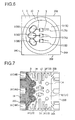
FIG. 6 is a top view showing a surface-mountedLED 1 as an electronic component of the second embodiment.FIG. 7 is a bottom view showing the surface-mountedLED 1.FIG. 8 is a bottom view showing a state ofFIG. 7 with coating 19 (hatched portion) omitted. For explanatory purposes, portions the same as those in the first embodiment shown inFIGS. 1 to 4 described above are provided with the same numerals. - In this embodiment, the electrode 4 (see
FIG. 1 ) is integrated with theelectrode 6 to form aground electrode 31. Moreover, theelectrodes ground electrode 32. As a result, the terminal section of theelectrode 16 is provided along theside end 20C (third side end), and the electrode 15 (lower electrode) is so provided as to extend to theside end 20D (fourth side end). Other portions are the same as those of the first embodiment. - One terminal of the
LED element 7 is connected to theelectrode 5, and the other terminal thereof is connected to theground electrode 31. Theground electrodes holes 13 and 14 (seeFIG. 1 ), and theground electrode 32 is connected to a ground section of the device loaded with the surface-mountedLED 1. - According to this embodiment, the same effects as those of the first embodiment can be provided. Moreover, heat generated at the
LED element 7 is radiated via theground electrodes LED 1. - Next,
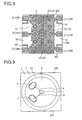
FIG. 9 is a top view showing a surface-mountedLED 1 as an electronic component of the third embodiment.FIG. 10 is a bottom view showing the surface-mountedLED 1.FIG. 11 is a bottom view showing a state ofFIG. 10 with coating 19 (hatched portion) omitted. For explanatory purposes, portions the same as those in the first embodiment shown inFIGS. 1 to 4 described above are provided with the same numerals. - In this embodiment, the terminal sections of the
electrodes side end 20C (third side end) of thecircuit board 2, and theelectrode 15 on the lower surface side is so provided as to extend to theside end 20D (fourth side end) of thecircuit board 2. To oneLED element 7, a voltage is applied via the terminal sections of theelectrodes side end 20C. Moreover, at theside end 20D, the throughhole 13 is provided which connects together theelectrode 4 and theelectrode 15. As a result, thedepressions 18 of a comb-like shape along a planar shape of the throughhole 13 are formed along theside end 20D. Other portions are the same as those of the first embodiment. - According to this embodiment, the same effects as the first embodiment can be provided. Moreover, wide areas of the
electrodes LED 1. In particular, when the number ofLED elements 7 loaded is small, the terminal sections can easily be collected at one side of the surface-mountedLED 1, thus permitting improvement in the heat radiation performance to be achieved by this embodiment. - Next,
FIG. 12 is a perspective view showing a surface-mountedLED 1 as an electronic component of the fourth embodiment. For explanatory purposes, portions the same as those of the first embodiments shown inFIGS. 1 to 4 described above are provided with the same numerals. This embodiment differs form the first embodiment in that the coating material 23 (seeFIG. 1 ) filled in theempty space 22 is omitted. This embodiment is the same as the first embodiment in the other configurations. - This embodiment can be carried out by omitting the resin filling process as the fourth process in the manufacturing processes of the surface-mounted
LED 1 shown inFIG. 5 described above. Since thecoating material 23 is omitted, the insulation performance deteriorates compared to the first embodiment, but good practicability can be achieved by ensuring the insulation distance between theframe 3 and thecircuit board 2 by theempty space 22. - At the time of forming the
grooves 28 in the third process ofFIG. 5 described above, the depth of thegrooves 28 may be made smaller than the thickness of thecircuit board 2. However, making the depth of thegrooves 28 larger than or equal to the thickness of thecircuit board 2 is preferable since it improves the insulation performance. Moreover, the depth of thegrooves 28 may be set at such a depth that does not permit penetration through theframe 3. When thecircuit board 2 is fixed at a section where soldering paste is applied by using a metal mask or the like, the depth of thegrooves 28 may be set so that it becomes higher (deeper) than the thickness (height) of this soldering paste. This can avoid insulation failure as a result of soldering, which is more preferable. -
Ground electrodes 31 and 32 (seeFIGS. 6 and 7 ) the same as those of the second embodiment may be provided, and terminal sections of theelectrodes side end 20D as is the case with the third embodiment. - Next,
FIG. 13 is a perspective view showing a surface-mountedLED 1 as an electronic component of the fifth embodiment. For explanatory purposes, portions the same as those of the first embodiments shown inFIGS. 1 to 4 described above are provided with the same numerals. This embodiment differs form the first embodiment in that the coating material 23 (seeFIG. 1 ) filled in theempty space 22 is a coating of a predetermined thickness. This embodiment is the same as the first embodiment in the other configurations. - Since the insulation distance can be ensured with the
empty space 22 and thecoating material 23, the insulation performance equivalent to that of the first embodiment can be ensured. Thecoating material 23 may be an insulating material as is the case with the first embodiment, or may be a conducting material. - Using a harder material for the
coating material 23 than a material forming theframe 3 is preferable since it suppresses occurrence of metal burr. When a conducting material is used as thecoating material 23, a metal material capable of preventing the occurrence of metal burr in theframe 3 can be used. As such a metal material, a hard metal material of nickel, chrome, titanium, or the like can be used. - Moreover, when a main material of the
frame 3 is formed of aluminum, magnesium, or the like, the surface of theframe 3 may be subjected to chemical conversion treatment (alumite treatment) to form thecoating material 23 composed of an insulating body. For example, when theframe 3 is of aluminum, the Vickers hardness (Hv) after typical alumite treatment is 200 to 250, and the Vickers hardness (Hv) after hard alumite treatment is 400 to 450. Therefore, the alumite portion can be used as thecoating material 23. - Moreover, the typical film thickness of alumite is approximately 20 µm, but can be thickened to approximately 100 µm. Thus, the use of thick-filmed alumite as the
coating material 23 can improve effect of insulation and effect of preventing metal burr. -
Ground electrodes 31 and 32 (seeFIGS. 6 and 7 ) the same as those of the second embodiment may be provided, and terminal sections of theelectrodes side end 20D as is the case with the third embodiment. - In the first to fifth embodiments, the invention is also applicable to an electronic component having as a heat-generating element a circuit element which has resistance components such as a chip resistor, an IC, etc. in addition to the LED element.
- According to the present invention, the invention can be used for an electronic component having a frame fixed on the upper surface of a circuit board. More specifically, the invention is applicable to a surface-mounted LED used as a light source for switch inner illumination, an LED display, a backlight light source, an optical printer head, a camera flash, or the like.
Claims (11)
- An electronic component comprising a circuit board having a plurality of electrodes on upper and lower surface of an insulating substrate and a thermogenic circuit element fixed to an upper surface of the circuit board, the electronic component further comprising:an upper electrode on which the circuit element is placed;a through hole penetrating through the insulating substrate; anda lower electrode formed on a lower surface side in a range from a first side end of the circuit board to a second side end thereof opposing the first side end, the lower electrode being connected to the upper electrode via the through hole.
- The electronic component according to claim 1,
wherein the upper electrode and the lower electrode are adapted to be electrically nonpolar. - The electronic component according to claim 2,
wherein terminal sections of a plurality of polar electrodes are arranged along opposing third and fourth side ends extending in a direction crossing the first and second side ends. - The electronic component according to claim 3,
wherein the lower electrode has a wider area than each of the polar electrodes. - The electronic component according to claim 2,
wherein the terminal sections of the polar electrodes are arranged along the third side end extending in the direction crossing the first and second side ends, and the lower electrode is provided in a manner such as to extend to the fourth side end opposing the third side end. - The electronic component according to claim 5,
wherein the upper electrode and the lower electrode are grounded. - The electronic component according to any of claims 1 to 6,
wherein a depression in a shape along the through hole is formed on a surface of the lower electrode. - The electronic component according to claim 7,
wherein a joint surface between the upper electrode and the lower electrode is composed of an upper surface of the through hole. - The electronic component according to claim 7,
wherein the depression is arranged near the first and second side ends. - The electronic component according to any of claims 1 to 6,
wherein a frame enclosing the surrounding of the circuit element and composed of a good heat conductor is provided in contact with the upper electrode. - The electronic component according to claim 10,
wherein the circuit element is composed of an LED element, and emitted light of the LED element is reflected by the frame
Applications Claiming Priority (2)
| Application Number | Priority Date | Filing Date | Title |
|---|---|---|---|
| JP2006166175 | 2006-06-15 | ||
| PCT/JP2007/060885 WO2007145074A1 (en) | 2006-06-15 | 2007-05-29 | Electronic component |
Publications (1)
| Publication Number | Publication Date |
|---|---|
| EP2034528A1 true EP2034528A1 (en) | 2009-03-11 |
Family
ID=38831592
Family Applications (1)
| Application Number | Title | Priority Date | Filing Date |
|---|---|---|---|
| EP07744305A Withdrawn EP2034528A1 (en) | 2006-06-15 | 2007-05-29 | Electronic component |
Country Status (5)
| Country | Link |
|---|---|
| US (1) | US20090314534A1 (en) |
| EP (1) | EP2034528A1 (en) |
| JP (1) | JP4854738B2 (en) |
| TW (1) | TW200807764A (en) |
| WO (1) | WO2007145074A1 (en) |
Families Citing this family (5)
| Publication number | Priority date | Publication date | Assignee | Title |
|---|---|---|---|---|
| JP2009289810A (en) * | 2008-05-27 | 2009-12-10 | Toshiba Lighting & Technology Corp | Illuminator |
| US8525040B2 (en) * | 2008-08-29 | 2013-09-03 | Kyocera Corporation | Circuit board and its wire bonding structure |
| JP5126638B2 (en) * | 2012-02-17 | 2013-01-23 | 東芝ライテック株式会社 | Light emitting device and lighting apparatus |
| TWI556478B (en) * | 2014-06-30 | 2016-11-01 | 億光電子工業股份有限公司 | Light-emitting diode device |
| CN215813649U (en) * | 2020-04-13 | 2022-02-11 | 日亚化学工业株式会社 | Planar light source |
Family Cites Families (19)
| Publication number | Priority date | Publication date | Assignee | Title |
|---|---|---|---|---|
| US5024966A (en) * | 1988-12-21 | 1991-06-18 | At&T Bell Laboratories | Method of forming a silicon-based semiconductor optical device mount |
| JPH1174651A (en) * | 1997-03-13 | 1999-03-16 | Ibiden Co Ltd | Printed wiring board and manufacturing method thereof |
| JP2943788B2 (en) * | 1997-04-10 | 1999-08-30 | 日立エーアイシー株式会社 | Wiring board for mounting electronic components |
| TW507482B (en) * | 2000-06-09 | 2002-10-21 | Sanyo Electric Co | Light emitting device, its manufacturing process, and lighting device using such a light-emitting device |
| US6657237B2 (en) * | 2000-12-18 | 2003-12-02 | Samsung Electro-Mechanics Co., Ltd. | GaN based group III-V nitride semiconductor light-emitting diode and method for fabricating the same |
| JP3891115B2 (en) * | 2001-04-17 | 2007-03-14 | 日亜化学工業株式会社 | Light emitting device |
| JP3991624B2 (en) * | 2001-06-26 | 2007-10-17 | 日亜化学工業株式会社 | Surface mount type light emitting device and manufacturing method thereof |
| US6531328B1 (en) * | 2001-10-11 | 2003-03-11 | Solidlite Corporation | Packaging of light-emitting diode |
| KR100439402B1 (en) * | 2001-12-24 | 2004-07-09 | 삼성전기주식회사 | Light emission diode package |
| KR100693969B1 (en) * | 2003-03-10 | 2007-03-12 | 도요다 고세이 가부시키가이샤 | Solid element device and manufacturing method thereof |
| EP1605524B1 (en) * | 2003-03-18 | 2010-06-30 | Sumitomo Electric Industries, Ltd. | Light emitting element mounting member, and semiconductor device using the same |
| KR20040092512A (en) * | 2003-04-24 | 2004-11-04 | (주)그래픽테크노재팬 | A semiconductor light emitting device with reflectors having a cooling function |
| WO2004105142A1 (en) * | 2003-05-26 | 2004-12-02 | Matsushita Electric Works, Ltd. | Light-emitting device |
| JP2005079329A (en) * | 2003-08-29 | 2005-03-24 | Stanley Electric Co Ltd | Surface mount type light emitting diode |
| JP4325412B2 (en) * | 2004-01-21 | 2009-09-02 | 日亜化学工業株式会社 | LIGHT EMITTING DEVICE AND LIGHT EMITTING DEVICE MANUFACTURING METHOD |
| JP2006186297A (en) * | 2004-12-03 | 2006-07-13 | Toshiba Corp | Semiconductor light emitting device and manufacturing method thereof |
| US7411225B2 (en) * | 2005-03-21 | 2008-08-12 | Lg Electronics Inc. | Light source apparatus |
| KR100593937B1 (en) * | 2005-03-30 | 2006-06-30 | 삼성전기주식회사 | LED package using Si substrate and manufacturing method thereof |
| JP2007165803A (en) * | 2005-12-16 | 2007-06-28 | Sharp Corp | Light emitting device |
-
2007
- 2007-05-29 WO PCT/JP2007/060885 patent/WO2007145074A1/en not_active Ceased
- 2007-05-29 US US12/301,265 patent/US20090314534A1/en not_active Abandoned
- 2007-05-29 EP EP07744305A patent/EP2034528A1/en not_active Withdrawn
- 2007-05-29 JP JP2008521140A patent/JP4854738B2/en active Active
- 2007-05-30 TW TW096119304A patent/TW200807764A/en unknown
Also Published As
| Publication number | Publication date |
|---|---|
| US20090314534A1 (en) | 2009-12-24 |
| WO2007145074A1 (en) | 2007-12-21 |
| JPWO2007145074A1 (en) | 2009-10-29 |
| TW200807764A (en) | 2008-02-01 |
| JP4854738B2 (en) | 2012-01-18 |
Similar Documents
| Publication | Publication Date | Title |
|---|---|---|
| US9490236B2 (en) | Light-emitting device and lighting device provided with the same | |
| US8035121B2 (en) | Package for light emitting device having a lens spaced from a light emitting device module | |
| EP2182783A2 (en) | Light-emitting module and illuminating apparatus | |
| EP1890343A1 (en) | Substrate for light-emitting device mounting, light-emitting device module, illuminating device, display and traffic signal device | |
| KR100646093B1 (en) | Light emitting device package | |
| EP2023413A1 (en) | Electronic component and method for manufacturing same | |
| TW200828635A (en) | Light emitting device, its manufacturing method and its mounted substrate | |
| KR20120118686A (en) | Light emitting device module | |
| JP2009054801A (en) | Heat dissipation member and light emitting module including the same | |
| JP2010097982A (en) | Light-emitting device | |
| JP2008235580A (en) | Manufacturing method of semiconductor device | |
| US20090314534A1 (en) | Electronic component | |
| JP2009194213A (en) | Electronic components | |
| KR20090082470A (en) | Light emitting device, manufacturing method thereof and mounting substrate | |
| JP4187239B2 (en) | High brightness light emitting device and manufacturing method thereof | |
| KR101719692B1 (en) | Printed Circuit Board, Manufacturing method thereof, LED module and LED lamp with using the same | |
| KR101886715B1 (en) | Light emitting device | |
| JP2008147513A (en) | Light emitting device | |
| KR20130079921A (en) | Printed circuit board | |
| CN100570907C (en) | light emitting structure | |
| KR101920211B1 (en) | Light emitting device array | |
| JP7557129B2 (en) | Surface emitting light source and its manufacturing method | |
| JP5999341B2 (en) | Light emitting device and lighting device | |
| JP2023086322A (en) | Light emitting device and manufacturing method thereof | |
| JP2001044579A (en) | Hybrid integrated circuit device |
Legal Events
| Date | Code | Title | Description |
|---|---|---|---|
| PUAI | Public reference made under article 153(3) epc to a published international application that has entered the european phase |
Free format text: ORIGINAL CODE: 0009012 |
|
| 17P | Request for examination filed |
Effective date: 20081210 |
|
| AK | Designated contracting states |
Kind code of ref document: A1 Designated state(s): AT BE BG CH CY CZ DE DK EE ES FI FR GB GR HU IE IS IT LI LT LU LV MC MT NL PL PT RO SE SI SK TR |
|
| AX | Request for extension of the european patent |
Extension state: AL BA HR MK RS |
|
| RBV | Designated contracting states (corrected) |
Designated state(s): AT DE FR GB |
|
| RBV | Designated contracting states (corrected) |
Designated state(s): DE FR GB NL |
|
| DAX | Request for extension of the european patent (deleted) | ||
| RBV | Designated contracting states (corrected) |
Designated state(s): DE FR GB NL |
|
| STAA | Information on the status of an ep patent application or granted ep patent |
Free format text: STATUS: THE APPLICATION HAS BEEN WITHDRAWN |
|
| 18W | Application withdrawn |
Effective date: 20120215 |