EP2027608B1 - Procédé de réalisation d'un dispositif microélectronique émetteur de lumière à nanofils semi-conducteurs formés sur un substrat métallique - Google Patents
Procédé de réalisation d'un dispositif microélectronique émetteur de lumière à nanofils semi-conducteurs formés sur un substrat métallique Download PDFInfo
- Publication number
- EP2027608B1 EP2027608B1 EP07730017.6A EP07730017A EP2027608B1 EP 2027608 B1 EP2027608 B1 EP 2027608B1 EP 07730017 A EP07730017 A EP 07730017A EP 2027608 B1 EP2027608 B1 EP 2027608B1
- Authority
- EP
- European Patent Office
- Prior art keywords
- substrate
- layer
- metal
- microelectronic device
- wires
- Prior art date
- Legal status (The legal status is an assumption and is not a legal conclusion. Google has not performed a legal analysis and makes no representation as to the accuracy of the status listed.)
- Not-in-force
Links
Images



Classifications
-
- C—CHEMISTRY; METALLURGY
- C30—CRYSTAL GROWTH
- C30B—SINGLE-CRYSTAL GROWTH; UNIDIRECTIONAL SOLIDIFICATION OF EUTECTIC MATERIAL OR UNIDIRECTIONAL DEMIXING OF EUTECTOID MATERIAL; REFINING BY ZONE-MELTING OF MATERIAL; PRODUCTION OF A HOMOGENEOUS POLYCRYSTALLINE MATERIAL WITH DEFINED STRUCTURE; SINGLE CRYSTALS OR HOMOGENEOUS POLYCRYSTALLINE MATERIAL WITH DEFINED STRUCTURE; AFTER-TREATMENT OF SINGLE CRYSTALS OR A HOMOGENEOUS POLYCRYSTALLINE MATERIAL WITH DEFINED STRUCTURE; APPARATUS THEREFOR
- C30B25/00—Single-crystal growth by chemical reaction of reactive gases, e.g. chemical vapour-deposition growth
-
- C—CHEMISTRY; METALLURGY
- C30—CRYSTAL GROWTH
- C30B—SINGLE-CRYSTAL GROWTH; UNIDIRECTIONAL SOLIDIFICATION OF EUTECTIC MATERIAL OR UNIDIRECTIONAL DEMIXING OF EUTECTOID MATERIAL; REFINING BY ZONE-MELTING OF MATERIAL; PRODUCTION OF A HOMOGENEOUS POLYCRYSTALLINE MATERIAL WITH DEFINED STRUCTURE; SINGLE CRYSTALS OR HOMOGENEOUS POLYCRYSTALLINE MATERIAL WITH DEFINED STRUCTURE; AFTER-TREATMENT OF SINGLE CRYSTALS OR A HOMOGENEOUS POLYCRYSTALLINE MATERIAL WITH DEFINED STRUCTURE; APPARATUS THEREFOR
- C30B29/00—Single crystals or homogeneous polycrystalline material with defined structure characterised by the material or by their shape
- C30B29/10—Inorganic compounds or compositions
- C30B29/40—AIIIBV compounds wherein A is B, Al, Ga, In or Tl and B is N, P, As, Sb or Bi
- C30B29/403—AIII-nitrides
-
- C—CHEMISTRY; METALLURGY
- C30—CRYSTAL GROWTH
- C30B—SINGLE-CRYSTAL GROWTH; UNIDIRECTIONAL SOLIDIFICATION OF EUTECTIC MATERIAL OR UNIDIRECTIONAL DEMIXING OF EUTECTOID MATERIAL; REFINING BY ZONE-MELTING OF MATERIAL; PRODUCTION OF A HOMOGENEOUS POLYCRYSTALLINE MATERIAL WITH DEFINED STRUCTURE; SINGLE CRYSTALS OR HOMOGENEOUS POLYCRYSTALLINE MATERIAL WITH DEFINED STRUCTURE; AFTER-TREATMENT OF SINGLE CRYSTALS OR A HOMOGENEOUS POLYCRYSTALLINE MATERIAL WITH DEFINED STRUCTURE; APPARATUS THEREFOR
- C30B29/00—Single crystals or homogeneous polycrystalline material with defined structure characterised by the material or by their shape
- C30B29/60—Single crystals or homogeneous polycrystalline material with defined structure characterised by the material or by their shape characterised by shape
- C30B29/605—Products containing multiple oriented crystallites, e.g. columnar crystallites
-
- H—ELECTRICITY
- H10—SEMICONDUCTOR DEVICES; ELECTRIC SOLID-STATE DEVICES NOT OTHERWISE PROVIDED FOR
- H10H—INORGANIC LIGHT-EMITTING SEMICONDUCTOR DEVICES HAVING POTENTIAL BARRIERS
- H10H20/00—Individual inorganic light-emitting semiconductor devices having potential barriers, e.g. light-emitting diodes [LED]
- H10H20/01—Manufacture or treatment
- H10H20/011—Manufacture or treatment of bodies, e.g. forming semiconductor layers
- H10H20/013—Manufacture or treatment of bodies, e.g. forming semiconductor layers having light-emitting regions comprising only Group III-V materials
- H10H20/0133—Manufacture or treatment of bodies, e.g. forming semiconductor layers having light-emitting regions comprising only Group III-V materials with a substrate not being Group III-V materials
- H10H20/01335—Manufacture or treatment of bodies, e.g. forming semiconductor layers having light-emitting regions comprising only Group III-V materials with a substrate not being Group III-V materials the light-emitting regions comprising nitride materials
-
- H—ELECTRICITY
- H10—SEMICONDUCTOR DEVICES; ELECTRIC SOLID-STATE DEVICES NOT OTHERWISE PROVIDED FOR
- H10H—INORGANIC LIGHT-EMITTING SEMICONDUCTOR DEVICES HAVING POTENTIAL BARRIERS
- H10H20/00—Individual inorganic light-emitting semiconductor devices having potential barriers, e.g. light-emitting diodes [LED]
- H10H20/80—Constructional details
- H10H20/81—Bodies
- H10H20/813—Bodies having a plurality of light-emitting regions, e.g. multi-junction LEDs or light-emitting devices having photoluminescent regions within the bodies
-
- H—ELECTRICITY
- H10—SEMICONDUCTOR DEVICES; ELECTRIC SOLID-STATE DEVICES NOT OTHERWISE PROVIDED FOR
- H10H—INORGANIC LIGHT-EMITTING SEMICONDUCTOR DEVICES HAVING POTENTIAL BARRIERS
- H10H20/00—Individual inorganic light-emitting semiconductor devices having potential barriers, e.g. light-emitting diodes [LED]
- H10H20/80—Constructional details
- H10H20/81—Bodies
- H10H20/817—Bodies characterised by the crystal structures or orientations, e.g. polycrystalline, amorphous or porous
- H10H20/818—Bodies characterised by the crystal structures or orientations, e.g. polycrystalline, amorphous or porous within the light-emitting regions
-
- H—ELECTRICITY
- H10—SEMICONDUCTOR DEVICES; ELECTRIC SOLID-STATE DEVICES NOT OTHERWISE PROVIDED FOR
- H10H—INORGANIC LIGHT-EMITTING SEMICONDUCTOR DEVICES HAVING POTENTIAL BARRIERS
- H10H20/00—Individual inorganic light-emitting semiconductor devices having potential barriers, e.g. light-emitting diodes [LED]
- H10H20/80—Constructional details
- H10H20/81—Bodies
- H10H20/811—Bodies having quantum effect structures or superlattices, e.g. tunnel junctions
- H10H20/812—Bodies having quantum effect structures or superlattices, e.g. tunnel junctions within the light-emitting regions, e.g. having quantum confinement structures
-
- H—ELECTRICITY
- H10—SEMICONDUCTOR DEVICES; ELECTRIC SOLID-STATE DEVICES NOT OTHERWISE PROVIDED FOR
- H10H—INORGANIC LIGHT-EMITTING SEMICONDUCTOR DEVICES HAVING POTENTIAL BARRIERS
- H10H20/00—Individual inorganic light-emitting semiconductor devices having potential barriers, e.g. light-emitting diodes [LED]
- H10H20/80—Constructional details
- H10H20/81—Bodies
- H10H20/822—Materials of the light-emitting regions
- H10H20/824—Materials of the light-emitting regions comprising only Group III-V materials, e.g. GaP
- H10H20/825—Materials of the light-emitting regions comprising only Group III-V materials, e.g. GaP containing nitrogen, e.g. GaN
-
- H—ELECTRICITY
- H10—SEMICONDUCTOR DEVICES; ELECTRIC SOLID-STATE DEVICES NOT OTHERWISE PROVIDED FOR
- H10H—INORGANIC LIGHT-EMITTING SEMICONDUCTOR DEVICES HAVING POTENTIAL BARRIERS
- H10H20/00—Individual inorganic light-emitting semiconductor devices having potential barriers, e.g. light-emitting diodes [LED]
- H10H20/80—Constructional details
- H10H20/83—Electrodes
- H10H20/831—Electrodes characterised by their shape
-
- H—ELECTRICITY
- H10—SEMICONDUCTOR DEVICES; ELECTRIC SOLID-STATE DEVICES NOT OTHERWISE PROVIDED FOR
- H10H—INORGANIC LIGHT-EMITTING SEMICONDUCTOR DEVICES HAVING POTENTIAL BARRIERS
- H10H20/00—Individual inorganic light-emitting semiconductor devices having potential barriers, e.g. light-emitting diodes [LED]
- H10H20/80—Constructional details
- H10H20/85—Packages
- H10H20/851—Wavelength conversion means
Definitions
- the technical field to which the invention relates is that of microelectronics and optoelectronics and more specifically the production of light emitters based on semiconductor materials.
- the invention relates to a method for producing a light emitting device comprising a plurality of nanowires formed on a metal substrate.
- a light emitting microelectronic device for example of the LED type (LED for "Light Emitting Diode” in English, or light-emitting diode) can be carried out, in a current manner, using successive epitaxies of several layers. thin semiconductor materials. Sapphire-based substrates, or substrates based on silicon carbide are generally used to form this type of device. The size of these substrates is often less than 3 inches (7.62 centimeters), which limits the number of integrable LEDs on the same substrate.
- the next stack can be realized: on a sapphire-type substrate 1, an N-doped GaN-based buffer layer 2 is formed and used for a lower contacting point 3, then a plurality of quantum wells respectively formed in an InGaN-based layer and a layer superimposed GaN, then a layer 5 of magnesium-doped GaN and finally a thin layer 6 of highly doped GaN P on which an upper contact 7 is formed ( Figure 1A and Figure 1B ).
- the mismatch between the sapphire (substrate) and the GaN of the buffer layer is generally large, which induces a high dislocation rate in the other semiconductor layers.
- the realization of the lower contact requires etching of the active layer 4, which increases the production process. With such an arrangement of the lower contact, the current injection is not homogeneous on the underside of the diode.
- the active layer 4 is capable of emitting light in all directions.
- the sapphire (substrate) 1 being a transparent material at the emission wavelength of the diode, about half of the light emitted towards the back side is lost.
- the sapphire substrate being electrically insulating, a thin layer of doped semiconductor material is generally formed on the latter, in order to achieve a ground plane.
- the electrical conductivity of the layer which ensures the passage of the current is generally low.
- This significant heating due to poor dissipation of heat by the substrate 1 can induce rapid degradation of the material and reduce the reliability of the active layer of the LED.
- Such a type of heating may decrease the electrical properties of the active layer and impair the efficiency of the LED.
- the document US 2003/0168964 A1 presents a process for producing an LED formed of nanowires made on a semitransparent conductive substrate.
- the nanowires are grown on a semi-transparent ITO (ITO for Indium Tin Oxide) or ZnO-based conductive layer.
- ITO Indium Tin Oxide
- ZnO-based conductive layer The electrical performance and performance of such a device may be insufficient.
- the document WO 2004/087564 A1 presents another method of producing a light emitting microelectronic device comprising nanowires and using, this time, a catalyst for their growth.
- the document WO 2006/000790 A1 discloses a method of making microelectronic devices comprising growing on a support of a given material a plurality of wires of different material; wires capable of emitting light radiation.
- the document US 2005/0199886 A1 discloses a method of producing a light emitting microelectronic device comprising nanowires. A variety of growth substrates for these nanowires are contemplated herein.
- the growth of the son is directly carried out on a metal layer of said support.
- the metal support may comprise a substrate based on a metal or a metal alloy, the metal or the metal alloy comprising at least one of the following materials: iron, nickel, aluminum, silver, copper, stainless steel, iron alloy and Ni such as invar®.
- the wires formed in step a) may be in contact with the substrate.
- the wires formed in step a) may be in contact with said thin layer.
- Said thin layer is provided for reflecting said light radiation.
- the method may also comprise, prior to step a), the deposition of a layer of catalyst material on the metal support.
- the method may also comprise, between step a) and step b), the formation of an insulating layer for encapsulating the wires.
- the starting material of the process is a metal substrate 100, which may be based on a metal such as aluminum or silver or copper, or a metal alloy for example based on aluminum or of silver or copper or such as stainless steel or a FeNi alloy, comprising iron and nickel such as invar® (trademark registered by Goodfellow).
- the metal substrate 100 may have a thickness of, for example, between 10 ⁇ m and 10 mm, or for example of the order of 1 mm, and a surface area of, for example, between 100 mm 2 and 1 m 2 , or, for example, order of 300 mm 2 .
- a step of preparing the substrate 100, and in particular a given face thereof for the purpose of growing yarns based on one or more semiconductor materials can be achieved by means of a surface treatment, comprising for example a step of degreasing the substrate with a solvent for example based on acetone and ethanol, and a step removing roughness, for example using a polishing on a felt.
- a material 101 intended to serve as a catalyst may then be deposited in the form of a thin layer, for example of the order of 5 nanometers, on said given face of the substrate 100.
- the catalyst material 101 may be for example gold or nickel formed by evaporation.
- a plurality of so-called “nano-son" wires 102, based on one or more semiconductor materials capable of emitting light radiation, are grown on the substrate 100. Nano-wires 102 can be made by epitaxy.
- the nano-wires 102 are intended to grow in a direction producing a non-zero angle, for example in a direction orthogonal to the main plane of the substrate 100 (the main plane of the substrate 100 being defined as a plane passing through the substrate 100 and parallel on the plane [O; i ; k ] an orthogonal reference [O; i ; j ; k ] on the Figure 2A ).
- the nano-wires 102 that are grown can be formed of one or more portions comprising gallium nitride or gallium nitride-based compound.
- the metal substrate 100 may be placed for example in a chamber of a type MOCVD reactor (method of chemical vapor deposition of semiconductor material or metal from organic materials).
- the substrate 100 is raised to high temperature for example of the order of 500 to 800 ° C to bring the catalyst material 101 in the form of droplets and make it active. Then, one or more precursors are introduced into the reaction chamber.
- precursors such as trimethylgallium and ammonia may for example be injected into the chamber of the reactor.
- the N-type doping of the first portion 104 may be carried out using a silane injection.
- the temperature of the substrate 100 may be for example between 500 ° C and 1000 ° C.
- the chemical composition of the nano-wires 102 is intended to vary along their growth axis.
- the first portion 104 of the N-doped GaN quantum wires may be covered for example by a second portion 106 in which quantum wells based on InGaN and GaN may be formed.
- the second portion may be covered by a third portion 108, for example based on P-doped GaN, itself covered by a fourth portion 110 based on P ++-doped GaN, and used for example to make contact (s).
- P-type doping may be carried out for example by injection of an organometallic based on Mg.
- the nanowires 102 obtained may have a diameter (measured in a direction parallel to the vector i orthogonal reference [O; i ; j ; k ]) for example between 5 nanometers and 500 nanometers and a length for example between 100 nanometers and 10 micrometers (measured in a direction parallel to the vector j the [O; i ; j ; k ]).
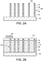
- the variation of chemical composition along the threads 102 is obtained by variation during the process of growth of the chemical composition and the concentration of the gases introduced into the reactor, combined with a variation of the temperature at which the substrate 100 is placed ( Figure 2A ).
- An encapsulation layer may then be formed on the substrate 100, and on either side of the nano-wires 102, so that the nano-wires 102 are inserted into the encapsulation layer 115.
- son 102 for example a portion of the fourth portion 110 thereof, protrudes from the encapsulation layer 115.
- the encapsulation layer 115 may be based on a dielectric material selected to impart a good flatness.
- the encapsulation layer 115 may for example be based on benzocyclobutene (BCB) or polystyrene and may be carried out for example by deposition.
- an upper contact 120 may be formed on the encapsulation layer 115, so as to cover the end of the wires protruding from the encapsulation layer 115.
- the upper contact 120 may be formed for example by deposition of a layer of an electrically conductive and semi-transparent material such as ITO (ITO for "indium tin oxide” in English), or a thin layer of Ti for example of the order of 5 nanometers covered by a other thin layer of Au for example of the order of 5 nanometers, or a deposit of carbon nanotubes.
- a metal contact zone 130 may be formed on the contact 120.
- the metal zone 130 may be made for example by deposition of a Ti layer of the order of 10 nanometers, then a layer of gold of the order of 200 nanometers, then by etching these layers, so as to form a pattern ( Figure 2B on which the device is shown in a sectional view, and Figure 2C , the device being shown in a view from above).
- the contact zone may comprise one or more parts 130a, 130b for conveying an electric current.
- the contact zone may optionally include a portion 130c provided to receive a weld.
- a layer of material 140 called "phosphor” (or “phosphor” in English), able to convert a quasi-monochromatic light into so-called white light can then be performed, so as to cover the metal zone 130 of contact and contact 120.
- the material 140 can be for example a YAG (YAG for yttrium-aluminum garnet in English or "yttrium-aluminum garnet”) material doped with cerium or Y 3 Al 5 O 12 : Ce 3+ ( 2D figure ).
- the substrate 100 being metallic, the latter may be intended to form a second contact, and may form for example a ground plane.
- the metal substrate 100 is also intended, according to the present invention, to reflect light radiation that can be emitted by the nano-wires 102.
- the reflectivity may be greater than 85% for radiation greater than 380 nm.
- a thin intermediate layer 201 to improve the phenomenon of growth and in particular nucleation of the nano-wires 102 on the surface of the metal substrate 100, prior to the catalyst deposition step 101, a thin intermediate layer 201, and which can be understood for example between several nanometers and several microns, can be formed on the metal substrate 100.
- the thin intermediate layer 201 is metallic and can be for example based on an iron silicide, or nickel, or silver, the aluminum, copper.
- the thin intermediate metal layer 201 is preferably electrically conductive. According to this variant in accordance with the method of the present invention, the thin intermediate metal layer 201 acts as a reflective layer and is thus able to reflect light rays intended to be emitted by the nano-wires 102.
Landscapes
- Chemical & Material Sciences (AREA)
- Engineering & Computer Science (AREA)
- Crystallography & Structural Chemistry (AREA)
- Materials Engineering (AREA)
- Metallurgy (AREA)
- Organic Chemistry (AREA)
- Chemical Kinetics & Catalysis (AREA)
- General Chemical & Material Sciences (AREA)
- Inorganic Chemistry (AREA)
- Led Devices (AREA)
Description
- Le domaine technique auquel se rapporte l'invention est celui de la microélectronique et de l'optoélectronique et plus spécifiquement la réalisation d'émetteurs de lumière à base de matériaux semi-conducteurs.
- L'invention concerne un procédé de réalisation d'un dispositif émetteur de lumière comprenant une pluralité de nanofils formés sur un substrat métallique.
- La réalisation d'un dispositif microélectronique émetteur de lumière, par exemple de type LED (LED pour « Light Emitting Diode » en anglais, ou diode électroluminescente) peut être effectuée, de manière courante, à l'aide d'épitaxies successives de plusieurs couches minces de matériaux semi-conducteurs. Des substrats à base de saphir, ou des substrats à base de carbure de silicium sont généralement utilisés pour former ce type de dispositif. La taille de ces substrats est souvent inférieure à 3 pouces (7,62 centimètres), ce qui limite le nombre de LED intégrables sur un même substrat.
- Par exemple, pour une LED émettant de la lumière à 450 nm, l'empilement suivant peut être réalisé : sur un substrat 1 de type saphir, une couche tampon 2 à base de GaN dopée N est formée et sert à une prise de contact inférieur 3, puis une pluralité de puits quantiques formés respectivement dans une couche à base d'InGaN et une couche à base de GaN superposées, puis une couche 5 de GaN dopé au magnésium et enfin une fine couche 6 de GaN fortement dopée P sur laquelle un contact supérieur 7 est formé (
figure 1A et figure 1B ). - Le désaccord de maille entre le saphir (substrat) et le GaN de la couche tampon est généralement important, ce qui induit un taux de dislocations élevé dans les autres couches semiconductrices. D'autre part, compte tenu du caractère isolant du saphir, la réalisation de la prise de contact inférieur, requiert une gravure de la couche active 4, qui alourdit le procédé de réalisation. Avec une telle disposition du contact inférieur, l'injection de courant n'est pas homogène sur la face inférieure de la diode. Par ailleurs, lorsque le dispositif est en fonctionnement la couche active 4 est susceptible d'émettre de la lumière dans toutes les directions. Le saphir (substrat) 1 étant un matériau transparent à la longueur d'onde d'émission de la diode, environ la moitié de la lumière émise en direction de la face arrière est perdue. Le substrat de saphir étant isolant électriquement, une fine couche de matériau semi-conducteur dopé est généralement formée sur ce dernier, pour pouvoir réaliser un plan de masse. La conductivité électrique de la couche qui assure le passage du courant, par exemple à base de GaN dopé N, est généralement faible. Lors du passage du courant au sein de la diode, il en résulte un échauffement important du dispositif par effet joule. Cet échauffement important dû à une mauvaise dissipation de la chaleur par le substrat 1 (la conductivité thermique des substrats de saphir étant généralement de l'ordre de 35 à 40 W/mK), peut induire des dégradations rapides du matériau et diminuer la fiabilité de la couche active de la LED. Un tel type d'échauffement peut diminuer les propriétés électriques de la couche active et détériorer le rendement de la LED.
- Dans le document
WO 02/080280 A1 - Le document
US 2003/0168964 A1 présente quant à lui un procédé de réalisation d'une LED formé de nano-fils réalisés sur un substrat conducteur semi-transparent. Dans ce procédé, la croissance des nanofils s'effectue sur une couche conductrice semi-transparente de type ITO (ITO pour Indium Tin Oxide) ou à base de ZnO. Les performances électriques et en termes de rendement d'un tel dispositif peuvent s'avérer insuffisantes. L'article de KIKUCHI A. et al.: "InGaN/GaN Multiple Quantum Disk Nanocolumn Light-Emitting Diodes Grown on (111) Si Substrate" JAPANESE JOURNAL OF APPLIED PHYSICS, vol. 43, no. 12A, 5 novembre 2004, pages L1524-L1526, présente un procédé de réalisation d'un dispositif microélectronique émetteur de lumière comprenant la croissance de nano-fils directement sur un substrat de silicium type N et orienté (111). Le documentWO 2004/087564 A1 présente un autre procédé de réalisation d'un dispositif microélectronique émetteur de lumière comprenant des nano-fils et utilisant, cette fois-ci, un catalyseur pour leur croissance. Le documentWO 2006/000790 A1 présente un procédé de réalisation de dispositifs microélectroniques comprenant la croissance sur un support en un matériau donné d'une pluralité de fils en un matériau différent; fils susceptibles d'émettre un rayonnement lumineux. Le documentUS 2005/0199886 A1 présente un procédé de réalisation d'un dispositif microélectronique émetteur de lumière comprenant des nano-fils. Une variété de substrats de croissance pour ces nano-fils est envisagée dans ce document. - Il se pose le problème de trouver un nouveau dispositif microélectronique émetteur de lumière à nano-fils semi-conducteurs ainsi qu'un nouveau procédé de réalisation d'un tel dispositif.
- L'invention concerne un procédé de réalisation d'un dispositif microélectronique émetteur de lumière, comprenant les étapes de :
- a) croissance sur un support métallique d'une pluralité de fils à base d'un ou plusieurs matériaux semi-conducteurs susceptibles d'émettre un rayonnement lumineux, ledit support métallique étant apte à réfléchir ledit rayonnement lumineux,
- b) formation d'au moins une zone de contact conductrice de l'électricité sur au moins un desdits fils.
- La croissance des fils est directement effectuée sur une couche métallique dudit support.
- Ainsi, la présente invention prévoit un procédé de réalisation d'un dispositif microélectronique émetteur de lumière, comprenant les étapes de :
- a) croissance sur une couche métallique continue de substrat appartenant à un support métallique, ou sur une fine couche métallique continue d'un support métallique, d'une pluralité de fils à base d'un ou plusieurs matériaux semi-conducteurs susceptibles d'émettre un rayonnement lumineux, ledit substrat ou ladite fine couche métallique étant apte à réfléchir ledit rayonnement lumineux,
- b) formation d'au moins une zone de contact conductrice de l'électricité sur au moins un desdits fils.
- Selon une possibilité, le support métallique peut comprendre un substrat à base d'un métal ou d'un alliage métallique, le métal ou l'alliage métallique comprenant au moins un des matériaux suivants : fer, nickel, aluminium, argent, cuivre, inox, d'alliage de fer et de Ni tel que l'invar®.
- Les fils formés à l'étape a) peuvent être en contact avec le substrat.
- Selon une variante, pour laquelle le substrat est recouvert d'une fine couche métallique, les fils formés à l'étape a) peuvent être en contact avec ladite fine couche.
- Ladite fine couche est prévue pour réfléchir ledit rayonnement lumineux.
- Le procédé peut également comprendre, préalablement à l'étape a), le dépôt d'une couche de matériau catalyseur sur le support métallique.
- Le procédé peut également comprendre, entre l'étape a) et l'étape b), la formation d'une couche isolante d'encapsulation des fils.
- La présente invention sera mieux comprise à la lecture de la description d'exemples de réalisation donnés, à titre purement indicatif et nullement limitatif, en faisant référence aux dessins annexés sur lesquels :
- les
figures 1A-1B , illustrent, un dispositif microélectronique de type LED selon l'art antérieur, respectivement suivant une vue en coupe et suivant une vue de dessus ; - les
figures 2A à 2D , illustrent un procédé suivant l'invention de réalisation d'un dispositif microélectronique de type LED doté de nano-fils formés sur un substrat métallique ; - la
figure 3 , illustre une variante de procédé suivant l'invention de réalisation d'un dispositif microélectronique de type LED doté de nano-fils formés sur un substrat métallique. - Des parties identiques, similaires ou équivalentes des différentes figures portent les mêmes références numériques de façon à faciliter le passage d'une figure à l'autre.
- Les différentes parties représentées sur les figures ne le sont pas nécessairement selon une échelle uniforme, pour rendre les figures plus lisibles.
- Un exemple de procédé de réalisation suivant l'invention d'un dispositif microélectronique émetteur de lumière (LED), va à présent être donné en liaison avec les
figures 2A-2D . Le matériau de départ du procédé est un substrat métallique 100, qui peut être à base d'un métal tel que de l'aluminium ou de l'argent ou du cuivre, ou d'un alliage métallique par exemple à base d'aluminium ou d'argent ou de cuivre ou tel que de l'inox ou un alliage FeNi, comportant du fer et du nickel tel que l'invar® (marque déposée par la société Goodfellow). Le substrat métallique 100 peut avoir une épaisseur comprise par exemple entre 10 µm et 10 mm, ou par exemple de l'ordre de 1 mm, et une surface par exemple comprise entre 100 mm2 et 1 m2, ou par exemple de l'ordre de 300 mm2. - Une étape de préparation du substrat 100, et en particulier d'une face donnée de ce dernier en vue d'une croissance de fils à base d'un ou plusieurs matériaux semi-conducteurs peut être réalisée à l'aide d'un traitement de surface, comprenant par exemple une étape de dégraissage du substrat à l'aide d'un solvant par exemple à base d'acétone et d'éthanol, et une étape d'élimination des rugosités par exemple à l'aide d'un polissage sur un feutre. Un matériau 101 destiné à servir de catalyseur peut être ensuite déposé sous forme d'une fine couche par exemple de l'ordre de 5 nanomètres, sur ladite face donnée du substrat 100. Le matériau catalyseur 101 peut être par exemple de l'or ou du nickel formé par évaporation. Ensuite, on fait croître sur le substrat 100, une pluralité de fils 102 dits « nano-fils », à base d'un ou plusieurs matériaux semi-conducteurs susceptibles d'émettre un rayonnement lumineux. Les nano-fils 102 peuvent être réalisés par épitaxie.
- Les nano-fils 102 sont destinés à croître dans une direction réalisant un angle non nul, par exemple dans une direction orthogonale avec le plan principal du substrat 100 (le plan principal du substrat 100 étant défini comme un plan passant par le substrat 100 et parallèle au plan [O;
i ;k ] d'un repère orthogonal [O;i ;j ;k ] sur lafigure 2A ). Les nano-fils 102 que l'on fait croître peuvent être formés d'une ou plusieurs portions comportant du nitrure de gallium ou un composé à base de nitrure de gallium. Pour cela, le substrat métallique 100 peut être placé par exemple dans une chambre d'un réacteur de type MOCVD (méthode de dépôt chimique en phase vapeur de matériau semi-conducteur ou de métal à partir de matériaux organiques). Le substrat 100 est porté à haute température par exemple de l'ordre de 500 à 800°C pour mettre le matériau catalyseur 101 sous forme de gouttelettes et le rendre actif. Ensuite, un ou plusieurs précurseurs sont introduits dans la chambre de réaction. Pour réaliser une première portion 104 des fils 102 à base d'un premier matériau, par exemple du GaN dopé N en contact avec le substrat métallique 100, des précurseurs tels que du triméthylgallium et de l'ammoniac peuvent être par exemple injectés dans la chambre du réacteur. Le dopage de type N de la première portion 104 peut être réalisé à l'aide d'une injection de silane. Pendant la croissance des nano-fils 102, la température du substrat 100 peut être comprise par exemple entre 500°C et 1000°C. La composition chimique des nano-fils 102 est destinée à varier le long de leur axe de croissance. La première portion 104 des fils quantiques de GaN dopé N, peut être recouverte par exemple par une deuxième portion 106 dans laquelle des puits quantiques, à base de InGaN et du GaN peuvent être formés. La deuxième portion peut être recouverte par une troisième portion 108, par exemple à base de GaN dopé P, elle même recouverte par une quatrième portion 110 à base de GaN dopé P++, et servant par exemple à la prise de contact (s). Le dopage de type P peut être réalisé par exemple par injection d'un organométallique à base de Mg. Une fois les nano-fils 102 formés, l'extrémité de ces derniers peut être recouverte du matériau catalyseur 101. Les nanofils 102 obtenus peuvent avoir un diamètre (mesuré dans une direction parallèle au vecteuri du repère orthogonal [O;i ;j ;k ]) compris par exemple entre 5 nanomètres et 500 nanomètres et une longueur comprise par exemple entre 100 nanomètres et 10 micromètres (mesurée dans une direction parallèle au vecteurj du repère [O;i ;j ;k ]). La variation de composition chimique le long des fils 102 est obtenue par variation au cours du procédé de croissance de la composition chimique et de la concentration des gaz introduits dans le réacteur, combinée à une variation de la température à laquelle le substrat 100 est placé (figure 2A ). - Une couche d'encapsulation peut être ensuite formée sur le substrat 100, et de part et d'autre des nano-fils 102, de sorte que les nano-fils 102 sont insérés dans la couche d'encapsulation 115. Une partie des nano-fils 102, par exemple une partie de la quatrième portion 110 de ces derniers, dépasse de la couche d'encapsulation 115. La couche d'encapsulation 115 peut être à base d'un matériau diélectrique choisi de manière à conférer une bonne planéité. La couche d'encapsulation 115 peut être par exemple à base de benzocyclobutène (BCB) ou de polystyrène et peut être réalisée par exemple par dépôt.
- Ensuite, un contact supérieur 120 peut être formé sur la couche d'encapsulation 115, de manière à recouvrir l'extrémité des fils dépassant de la couche d'encapsulation 115. Le contact supérieur 120 peut être formé par exemple par dépôt d'une couche d'un matériau conducteur de l'électricité et semi-transparent comme de l'ITO (ITO pour "indium tin oxide" en anglais), ou d'une fine couche de Ti par exemple de l'ordre de 5 nanomètres recouverte par une autre fine couche d'Au par exemple de l'ordre de 5 nanomètres, ou d'un dépôt de nanotubes de carbone.
- Ensuite, un zone métallique 130 de prise de contact peut être formée sur le contact 120. La zone métallique 130 peut être réalisée par exemple par dépôt d'une couche de Ti de l'ordre de 10 nanomètres, puis d'une couche d'or de l'ordre de 200 nanomètres, puis par gravure de ces couches, de manière à former un motif (
figure 2B sur laquelle le dispositif est représenté selon une vue en coupe, etfigure 2C , le dispositif étant représenté selon une vue de dessus). La zone de contact peut comporter une ou plusieurs parties 130a, 130b destinées à acheminer un courant électrique. La zone de contact peut éventuellement comporter une partie 130c prévue pour recevoir une soudure. - Une couche de matériau 140 dit « luminophore » (ou « phosphor » en anglais), apte à convertir une lumière quasi-monochromatique en lumière dite blanche peut être ensuite réalisée, de manière à recouvrir la zone métallique 130 de prise de contact et le contact 120. Le matériau 140 peut être par exemple un matériau YAG (YAG pour « yttrium-aluminium garnet » en anglais ou « grenat d'yttrium-aluminium ») dopé au Cérium ou Y3Al5O12:Ce3+ (
figure 2D ). Le substrat 100 étant métallique, ce dernier peut être destiné à former un deuxième contact, et peut former par exemple un plan de masse. Le substrat métallique 100 est également destiné, selon la présente invention, à réfléchir des rayonnements lumineux susceptibles d'être émis par les nano-fils 102. Un rayonnement lumineux émis en direction de la face arrière du dispositif, autrement dit en direction du substrat 100, est ainsi apte à être réfléchi et redirigé en direction de la face avant. Dans un cas où le substrat 100 est à base d'argent ou d'aluminium, la réflectivité peut être supérieure à 85 % pour des rayonnements supérieurs à 380 nm. - Selon une variante de procédé en accord avec la présente invention (
figure 3 ), pour améliorer le phénomène de croissance et en particulier de nucléation des nano-fils 102 à la surface du substrat métallique 100, préalablement à l'étape de dépôt du catalyseur 101, une fine couche intermédiaire 201, et qui peut être comprise par exemple entre plusieurs nanomètres et plusieurs microns, peut être formée sur le substrat métallique 100. La fine couche intermédiaire 201 est métallique et peut être par exemple à base d'un siliciure de fer, ou du nickel, ou de l'argent, de l'aluminium, du cuivre. La fine couche métallique intermédiaire 201 est de préférence conductrice de l'électricité. Selon cette variante en accord avec le procédé de la présente invention, la fine couche métallique intermédiaire 201 joue le rôle d'une couche réfléchissante et est ainsi apte à réfléchir des rayonnements lumineux destinés à être émis par les nano-fils 102.
Claims (4)
- Procédé de réalisation d'un dispositif microélectronique émetteur de lumière, comprenant les étapes de :a) croissance sur une couche métallique continue de substrat (100) appartenant à un support métallique, ou sur une fine couche métallique (201) d'un support métallique, d'une pluralité de fils (102) à base d'un ou plusieurs matériaux semi-conducteurs susceptibles d'émettre un rayonnement lumineux, ledit substrat ou ladite fine couche (201) métallique, étant apte à réfléchir ledit rayonnement lumineux,b) formation d'au moins une zone de contact conductrice (120) de l'électricité sur au moins un desdits fils.
- Procédé de réalisation d'un dispositif microélectronique émetteur de lumière selon la revendication 1, dans lequel ledit substrat (100) est à base d'un métal ou d'un alliage métallique comprenant l'un des matériaux suivants : fer, nickel, aluminium, argent, cuivre.
- Procédé de réalisation d'un dispositif microélectronique émetteur de lumière selon l'une des revendications 1 ou 2, comprenant préalablement à l'étape a), le dépôt d'une couche de matériau catalyseur (101) sur le support métallique.
- Procédé de réalisation d'un dispositif microélectronique émetteur de lumière selon l'une des revendications 1 à 3, comprenant en outre : entre l'étape a) et l'étape b), la formation d'une couche isolante d'encapsulation (115) des fils.
Applications Claiming Priority (2)
| Application Number | Priority Date | Filing Date | Title |
|---|---|---|---|
| FR0652075A FR2902237B1 (fr) | 2006-06-09 | 2006-06-09 | Procede de realisation d'un dispositif microelectronique emetteur de lumiere a nanofils semi-conducteurs formes sur un substrat metallique |
| PCT/EP2007/055661 WO2007141333A1 (fr) | 2006-06-09 | 2007-06-08 | Procede de realisation d'un dispositif microelectronique emetteur de lumiere a nanofils semi-conducteurs formes sur un substrat metallique |
Publications (2)
| Publication Number | Publication Date |
|---|---|
| EP2027608A1 EP2027608A1 (fr) | 2009-02-25 |
| EP2027608B1 true EP2027608B1 (fr) | 2018-08-15 |
Family
ID=37400917
Family Applications (1)
| Application Number | Title | Priority Date | Filing Date |
|---|---|---|---|
| EP07730017.6A Not-in-force EP2027608B1 (fr) | 2006-06-09 | 2007-06-08 | Procédé de réalisation d'un dispositif microélectronique émetteur de lumière à nanofils semi-conducteurs formés sur un substrat métallique |
Country Status (4)
| Country | Link |
|---|---|
| US (1) | US8535962B2 (fr) |
| EP (1) | EP2027608B1 (fr) |
| FR (1) | FR2902237B1 (fr) |
| WO (1) | WO2007141333A1 (fr) |
Families Citing this family (38)
| Publication number | Priority date | Publication date | Assignee | Title |
|---|---|---|---|---|
| WO2009096961A1 (fr) * | 2008-01-30 | 2009-08-06 | Hewlett-Packard Development Company, L.P. | Nanostructures et leurs procédés de fabrication |
| KR100956499B1 (ko) * | 2008-08-01 | 2010-05-07 | 주식회사 실트론 | 금속층을 가지는 화합물 반도체 기판, 그 제조 방법 및이를 이용한 화합물 반도체 소자 |
| FR2949278B1 (fr) | 2009-08-18 | 2012-11-02 | Commissariat Energie Atomique | Procede de fabrication d'un dispositif d'emission de lumiere a base de diodes electroluminescentes |
| DE102009043414B4 (de) * | 2009-09-29 | 2016-09-22 | Siemens Aktiengesellschaft | Dreidimensionale Mikro-Struktur, Anordnung mit mindestens zwei dreidimensionalen Mikro-Strukturen, Verfahren zum Herstellen der Mikro-Struktur und Verwendung der Mikro-Struktur |
| TWI476958B (zh) * | 2009-12-23 | 2015-03-11 | 鴻海精密工業股份有限公司 | 發光二極體封裝結構及其封裝方法 |
| FR2975532B1 (fr) | 2011-05-18 | 2013-05-10 | Commissariat Energie Atomique | Connexion electrique en serie de nanofils emetteurs de lumiere |
| DE102011118273A1 (de) * | 2011-11-11 | 2013-05-16 | Forschungsverbund Berlin E.V. | Herstellung einer Halbleitereinrichtung mit mindestens einem säulen- oder wandförmigen Halbleiter-Element |
| FR2985989B1 (fr) | 2012-01-23 | 2017-03-03 | Commissariat Energie Atomique | Procede d'isolation de nanofils ou de microfils |
| TWI478382B (zh) | 2012-06-26 | 2015-03-21 | Lextar Electronics Corp | 發光二極體及其製造方法 |
| TWI476953B (zh) * | 2012-08-10 | 2015-03-11 | Univ Nat Taiwan | 半導體發光元件及其製作方法 |
| FR3000298B1 (fr) * | 2012-12-20 | 2015-01-16 | Aledia | Procede optimise de fabrication de nanofils electroluminescents |
| TWI672826B (zh) * | 2017-07-13 | 2019-09-21 | 晶元光電股份有限公司 | 發光元件 |
| CN114464713B (zh) | 2017-07-13 | 2025-03-25 | 晶元光电股份有限公司 | 发光元件 |
| US11961875B2 (en) | 2017-12-20 | 2024-04-16 | Lumileds Llc | Monolithic segmented LED array architecture with islanded epitaxial growth |
| US20190198564A1 (en) | 2017-12-20 | 2019-06-27 | Lumileds Llc | Monolithic segmented led array architecture with islanded epitaxial growth |
| US11271033B2 (en) | 2018-09-27 | 2022-03-08 | Lumileds Llc | Micro light emitting devices |
| US11777059B2 (en) | 2019-11-20 | 2023-10-03 | Lumileds Llc | Pixelated light-emitting diode for self-aligned photoresist patterning |
| US11942507B2 (en) | 2020-03-11 | 2024-03-26 | Lumileds Llc | Light emitting diode devices |
| US11848402B2 (en) | 2020-03-11 | 2023-12-19 | Lumileds Llc | Light emitting diode devices with multilayer composite film including current spreading layer |
| US11569415B2 (en) | 2020-03-11 | 2023-01-31 | Lumileds Llc | Light emitting diode devices with defined hard mask opening |
| US11735695B2 (en) | 2020-03-11 | 2023-08-22 | Lumileds Llc | Light emitting diode devices with current spreading layer |
| US11626538B2 (en) | 2020-10-29 | 2023-04-11 | Lumileds Llc | Light emitting diode device with tunable emission |
| US11901491B2 (en) | 2020-10-29 | 2024-02-13 | Lumileds Llc | Light emitting diode devices |
| US12040432B2 (en) | 2020-10-30 | 2024-07-16 | Lumileds Llc | Light emitting diode devices with patterned TCO layer including different thicknesses |
| US11955583B2 (en) | 2020-12-01 | 2024-04-09 | Lumileds Llc | Flip chip micro light emitting diodes |
| US11705534B2 (en) | 2020-12-01 | 2023-07-18 | Lumileds Llc | Methods of making flip chip micro light emitting diodes |
| US11600656B2 (en) | 2020-12-14 | 2023-03-07 | Lumileds Llc | Light emitting diode device |
| US12484346B2 (en) | 2021-09-03 | 2025-11-25 | Lumileds Singapore Pte. Ltd. | Light emitting diode devices with bonding and/or ohmic contact-reflective material |
| US12402440B2 (en) | 2021-09-03 | 2025-08-26 | Lumileds Llc | Light emitting diode devices with bonding and/or ohmic contact-reflective material |
| US12419137B2 (en) | 2021-09-10 | 2025-09-16 | Lumileds Llc | Light emitting diodes with segmented anodes by pixel |
| US12431478B2 (en) | 2021-09-29 | 2025-09-30 | Lumileds Singapore Pte. Ltd. | Hybrid CMOS micro-LED display layout |
| US12568728B2 (en) | 2021-09-29 | 2026-03-03 | Lumileds Singapore Pte. Ltd. | Hybrid CMOS micro-LED display layout |
| US12433080B2 (en) | 2021-09-29 | 2025-09-30 | Lumileds Singapore Pte. Ltd. | Hybrid CMOS micro-LED display layout |
| US11935987B2 (en) | 2021-11-03 | 2024-03-19 | Lumileds Llc | Light emitting diode arrays with a light-emitting pixel area |
| US12604572B2 (en) | 2021-11-12 | 2026-04-14 | Lumileds Singapore Pte. Ltd. | Thin-film LED array with low refractive index patterned structures and reflector |
| US12490570B2 (en) | 2021-11-12 | 2025-12-02 | Lumileds Singapore Pte. Ltd. | Thin-film LED array with low refractive index patterned structures |
| US12588326B2 (en) | 2021-11-12 | 2026-03-24 | Lumileds Singapore Pte. Ltd. | Composite cathode contact for monolithically integrated micro-LEDs, mini-LEDs and LED arrays |
| CN117637935A (zh) * | 2023-12-12 | 2024-03-01 | 河源市众拓光电科技有限公司 | 一种白光led制备方法及白光led |
Citations (1)
| Publication number | Priority date | Publication date | Assignee | Title |
|---|---|---|---|---|
| US20050199886A1 (en) * | 2004-03-10 | 2005-09-15 | Siltron Inc. | Nitride semiconductor device and method of manufacturing the same |
Family Cites Families (11)
| Publication number | Priority date | Publication date | Assignee | Title |
|---|---|---|---|---|
| DE60118052T2 (de) * | 2000-04-13 | 2006-10-26 | Jsr Corp. | Überzugsmittel, Verfahren zur Herstellung, gehärtetes Produkt und Beschichtungsfilm |
| US6996147B2 (en) | 2001-03-30 | 2006-02-07 | The Regents Of The University Of California | Methods of fabricating nanostructures and nanowires and devices fabricated therefrom |
| TWI220319B (en) * | 2002-03-11 | 2004-08-11 | Solidlite Corp | Nano-wire light emitting device |
| EP1613549B1 (fr) * | 2003-04-04 | 2013-08-07 | QuNano AB | Structures de nanotrichites places avec precision, et leur procede de preparation |
| US7344753B2 (en) | 2003-09-19 | 2008-03-18 | The Board Of Trustees Of The University Of Illinois | Nanostructures including a metal |
| US20050253137A1 (en) * | 2003-11-20 | 2005-11-17 | President And Fellows Of Harvard College | Nanoscale arrays, robust nanostructures, and related devices |
| TWI229463B (en) * | 2004-02-02 | 2005-03-11 | South Epitaxy Corp | Light-emitting diode structure with electro-static discharge protection |
| US7528002B2 (en) * | 2004-06-25 | 2009-05-05 | Qunano Ab | Formation of nanowhiskers on a substrate of dissimilar material |
| KR100647288B1 (ko) * | 2004-09-13 | 2006-11-23 | 삼성전자주식회사 | 나노와이어 발광소자 및 그 제조방법 |
| US20060207647A1 (en) * | 2005-03-16 | 2006-09-21 | General Electric Company | High efficiency inorganic nanorod-enhanced photovoltaic devices |
| EP2410582B1 (fr) * | 2005-05-24 | 2019-09-04 | LG Electronics Inc. | Diode électroluminescente à nano-bâtonnets et procédé de fabrication d'une diode électroluminescente à nano-bâtonnets |
-
2006
- 2006-06-09 FR FR0652075A patent/FR2902237B1/fr not_active Expired - Fee Related
-
2007
- 2007-06-08 US US12/302,805 patent/US8535962B2/en not_active Expired - Fee Related
- 2007-06-08 WO PCT/EP2007/055661 patent/WO2007141333A1/fr not_active Ceased
- 2007-06-08 EP EP07730017.6A patent/EP2027608B1/fr not_active Not-in-force
Patent Citations (1)
| Publication number | Priority date | Publication date | Assignee | Title |
|---|---|---|---|---|
| US20050199886A1 (en) * | 2004-03-10 | 2005-09-15 | Siltron Inc. | Nitride semiconductor device and method of manufacturing the same |
Also Published As
| Publication number | Publication date |
|---|---|
| FR2902237A1 (fr) | 2007-12-14 |
| US8535962B2 (en) | 2013-09-17 |
| EP2027608A1 (fr) | 2009-02-25 |
| US20090246901A1 (en) | 2009-10-01 |
| WO2007141333A1 (fr) | 2007-12-13 |
| FR2902237B1 (fr) | 2008-10-10 |
Similar Documents
| Publication | Publication Date | Title |
|---|---|---|
| EP2027608A1 (fr) | Procede de realisation d'un dispositif microelectronique emetteur de lumiere a nanofils semi-conducteurs formes sur un substrat metallique | |
| US8470627B2 (en) | Method for manufacturing semiconductor light emitting device | |
| JP5383823B2 (ja) | ナノ構造デバイス | |
| EP3991216B1 (fr) | Procédé de fabrication d'un dispositif optoélectronique à diodes électroluminescentes de type axial | |
| EP2863444B1 (fr) | DEL à structure verticale | |
| US20090146142A1 (en) | Light-emitting device including nanorod and method of manufacturing the same | |
| EP3014665B1 (fr) | Dispositif optoélectronique à réflectivité améliorée et son procédé de fabrication | |
| KR101039988B1 (ko) | 발광 소자 및 그 제조방법 | |
| US9647174B2 (en) | Optoelectronic semiconductor chip | |
| CN101091234A (zh) | 用于光电子应用的基板的制造方法 | |
| CN108511567A (zh) | 与赝配电子和光电器件的平面接触 | |
| EP3090450B1 (fr) | Dispositif optoélectronique à éléments semiconducteurs et son procédé de fabrication | |
| WO2008154526A2 (fr) | Procédé de réalisation de contact de faible résistance | |
| US9142714B2 (en) | High power ultraviolet light emitting diode with superlattice | |
| KR20070046108A (ko) | 발광 소자 및 그 제조 방법 | |
| EP3053201B1 (fr) | Dispositif optoélectronique à diodes électroluminescentes | |
| US8431936B2 (en) | Method for fabricating a p-type semiconductor structure | |
| EP3164881B1 (fr) | Dispositif optoelectronique a elements semiconducteurs et son procede de fabrication | |
| FR3041476A1 (fr) | Dispositif electroluminescent a puits quantiques multiples | |
| EP3991213A1 (fr) | Procede d'homogeneisation de la section de nanofils pour diodes electroluminescentes |
Legal Events
| Date | Code | Title | Description |
|---|---|---|---|
| PUAI | Public reference made under article 153(3) epc to a published international application that has entered the european phase |
Free format text: ORIGINAL CODE: 0009012 |
|
| 17P | Request for examination filed |
Effective date: 20081201 |
|
| AK | Designated contracting states |
Kind code of ref document: A1 Designated state(s): AT BE BG CH CY CZ DE DK EE ES FI FR GB GR HU IE IS IT LI LT LU LV MC MT NL PL PT RO SE SI SK TR |
|
| AX | Request for extension of the european patent |
Extension state: AL BA HR MK RS |
|
| RIN1 | Information on inventor provided before grant (corrected) |
Inventor name: GENTILE, PASCAL Inventor name: GILET, PHILIPPE Inventor name: BARON, THIERRY Inventor name: FERRET, PIERRE Inventor name: TCHELNOKOV, ALEXEI |
|
| RAP1 | Party data changed (applicant data changed or rights of an application transferred) |
Owner name: COMMISSARIAT A L'ENERGIE ATOMIQUE ET AUX ENERGIES |
|
| 17Q | First examination report despatched |
Effective date: 20100419 |
|
| DAX | Request for extension of the european patent (deleted) | ||
| RAP1 | Party data changed (applicant data changed or rights of an application transferred) |
Owner name: CENTRE NATIONAL DE LA RECHERCHE SCIENTIFIQUE Owner name: COMMISSARIAT A L'ENERGIE ATOMIQUE ET AUX ENERGIES |
|
| STAA | Information on the status of an ep patent application or granted ep patent |
Free format text: STATUS: EXAMINATION IS IN PROGRESS |
|
| GRAP | Despatch of communication of intention to grant a patent |
Free format text: ORIGINAL CODE: EPIDOSNIGR1 |
|
| STAA | Information on the status of an ep patent application or granted ep patent |
Free format text: STATUS: GRANT OF PATENT IS INTENDED |
|
| RIC1 | Information provided on ipc code assigned before grant |
Ipc: C30B 29/40 20060101ALN20180216BHEP Ipc: C30B 29/62 20060101ALI20180216BHEP Ipc: H01L 33/38 20100101ALN20180216BHEP Ipc: H01L 33/50 20100101ALN20180216BHEP Ipc: H01L 33/32 20100101ALN20180216BHEP Ipc: H01L 33/06 20100101ALN20180216BHEP Ipc: C30B 25/00 20060101ALI20180216BHEP Ipc: H01L 33/18 20100101ALI20180216BHEP Ipc: H01L 33/00 20100101AFI20180216BHEP Ipc: H01L 33/08 20100101ALI20180216BHEP |
|
| INTG | Intention to grant announced |
Effective date: 20180307 |
|
| GRAS | Grant fee paid |
Free format text: ORIGINAL CODE: EPIDOSNIGR3 |
|
| GRAA | (expected) grant |
Free format text: ORIGINAL CODE: 0009210 |
|
| STAA | Information on the status of an ep patent application or granted ep patent |
Free format text: STATUS: THE PATENT HAS BEEN GRANTED |
|
| AK | Designated contracting states |
Kind code of ref document: B1 Designated state(s): AT BE BG CH CY CZ DE DK EE ES FI FR GB GR HU IE IS IT LI LT LU LV MC MT NL PL PT RO SE SI SK TR |
|
| REG | Reference to a national code |
Ref country code: CH Ref legal event code: EP Ref country code: GB Ref legal event code: FG4D Free format text: NOT ENGLISH Ref country code: AT Ref legal event code: REF Ref document number: 1030761 Country of ref document: AT Kind code of ref document: T Effective date: 20180815 |
|
| REG | Reference to a national code |
Ref country code: IE Ref legal event code: FG4D Free format text: LANGUAGE OF EP DOCUMENT: FRENCH |
|
| REG | Reference to a national code |
Ref country code: DE Ref legal event code: R096 Ref document number: 602007055743 Country of ref document: DE |
|
| REG | Reference to a national code |
Ref country code: NL Ref legal event code: MP Effective date: 20180815 |
|
| REG | Reference to a national code |
Ref country code: LT Ref legal event code: MG4D |
|
| REG | Reference to a national code |
Ref country code: AT Ref legal event code: MK05 Ref document number: 1030761 Country of ref document: AT Kind code of ref document: T Effective date: 20180815 |
|
| PG25 | Lapsed in a contracting state [announced via postgrant information from national office to epo] |
Ref country code: LT Free format text: LAPSE BECAUSE OF FAILURE TO SUBMIT A TRANSLATION OF THE DESCRIPTION OR TO PAY THE FEE WITHIN THE PRESCRIBED TIME-LIMIT Effective date: 20180815 Ref country code: FI Free format text: LAPSE BECAUSE OF FAILURE TO SUBMIT A TRANSLATION OF THE DESCRIPTION OR TO PAY THE FEE WITHIN THE PRESCRIBED TIME-LIMIT Effective date: 20180815 Ref country code: SE Free format text: LAPSE BECAUSE OF FAILURE TO SUBMIT A TRANSLATION OF THE DESCRIPTION OR TO PAY THE FEE WITHIN THE PRESCRIBED TIME-LIMIT Effective date: 20180815 Ref country code: GR Free format text: LAPSE BECAUSE OF FAILURE TO SUBMIT A TRANSLATION OF THE DESCRIPTION OR TO PAY THE FEE WITHIN THE PRESCRIBED TIME-LIMIT Effective date: 20181116 Ref country code: NL Free format text: LAPSE BECAUSE OF FAILURE TO SUBMIT A TRANSLATION OF THE DESCRIPTION OR TO PAY THE FEE WITHIN THE PRESCRIBED TIME-LIMIT Effective date: 20180815 Ref country code: BG Free format text: LAPSE BECAUSE OF FAILURE TO SUBMIT A TRANSLATION OF THE DESCRIPTION OR TO PAY THE FEE WITHIN THE PRESCRIBED TIME-LIMIT Effective date: 20181115 Ref country code: IS Free format text: LAPSE BECAUSE OF FAILURE TO SUBMIT A TRANSLATION OF THE DESCRIPTION OR TO PAY THE FEE WITHIN THE PRESCRIBED TIME-LIMIT Effective date: 20181215 Ref country code: AT Free format text: LAPSE BECAUSE OF FAILURE TO SUBMIT A TRANSLATION OF THE DESCRIPTION OR TO PAY THE FEE WITHIN THE PRESCRIBED TIME-LIMIT Effective date: 20180815 |
|
| PG25 | Lapsed in a contracting state [announced via postgrant information from national office to epo] |
Ref country code: ES Free format text: LAPSE BECAUSE OF FAILURE TO SUBMIT A TRANSLATION OF THE DESCRIPTION OR TO PAY THE FEE WITHIN THE PRESCRIBED TIME-LIMIT Effective date: 20180815 Ref country code: LV Free format text: LAPSE BECAUSE OF FAILURE TO SUBMIT A TRANSLATION OF THE DESCRIPTION OR TO PAY THE FEE WITHIN THE PRESCRIBED TIME-LIMIT Effective date: 20180815 |
|
| PG25 | Lapsed in a contracting state [announced via postgrant information from national office to epo] |
Ref country code: CZ Free format text: LAPSE BECAUSE OF FAILURE TO SUBMIT A TRANSLATION OF THE DESCRIPTION OR TO PAY THE FEE WITHIN THE PRESCRIBED TIME-LIMIT Effective date: 20180815 Ref country code: RO Free format text: LAPSE BECAUSE OF FAILURE TO SUBMIT A TRANSLATION OF THE DESCRIPTION OR TO PAY THE FEE WITHIN THE PRESCRIBED TIME-LIMIT Effective date: 20180815 Ref country code: EE Free format text: LAPSE BECAUSE OF FAILURE TO SUBMIT A TRANSLATION OF THE DESCRIPTION OR TO PAY THE FEE WITHIN THE PRESCRIBED TIME-LIMIT Effective date: 20180815 Ref country code: PL Free format text: LAPSE BECAUSE OF FAILURE TO SUBMIT A TRANSLATION OF THE DESCRIPTION OR TO PAY THE FEE WITHIN THE PRESCRIBED TIME-LIMIT Effective date: 20180815 |
|
| REG | Reference to a national code |
Ref country code: DE Ref legal event code: R097 Ref document number: 602007055743 Country of ref document: DE |
|
| PG25 | Lapsed in a contracting state [announced via postgrant information from national office to epo] |
Ref country code: SK Free format text: LAPSE BECAUSE OF FAILURE TO SUBMIT A TRANSLATION OF THE DESCRIPTION OR TO PAY THE FEE WITHIN THE PRESCRIBED TIME-LIMIT Effective date: 20180815 Ref country code: DK Free format text: LAPSE BECAUSE OF FAILURE TO SUBMIT A TRANSLATION OF THE DESCRIPTION OR TO PAY THE FEE WITHIN THE PRESCRIBED TIME-LIMIT Effective date: 20180815 |
|
| PLBE | No opposition filed within time limit |
Free format text: ORIGINAL CODE: 0009261 |
|
| STAA | Information on the status of an ep patent application or granted ep patent |
Free format text: STATUS: NO OPPOSITION FILED WITHIN TIME LIMIT |
|
| 26N | No opposition filed |
Effective date: 20190516 |
|
| PG25 | Lapsed in a contracting state [announced via postgrant information from national office to epo] |
Ref country code: SI Free format text: LAPSE BECAUSE OF FAILURE TO SUBMIT A TRANSLATION OF THE DESCRIPTION OR TO PAY THE FEE WITHIN THE PRESCRIBED TIME-LIMIT Effective date: 20180815 |
|
| PG25 | Lapsed in a contracting state [announced via postgrant information from national office to epo] |
Ref country code: MC Free format text: LAPSE BECAUSE OF FAILURE TO SUBMIT A TRANSLATION OF THE DESCRIPTION OR TO PAY THE FEE WITHIN THE PRESCRIBED TIME-LIMIT Effective date: 20180815 |
|
| REG | Reference to a national code |
Ref country code: CH Ref legal event code: PL |
|
| REG | Reference to a national code |
Ref country code: BE Ref legal event code: MM Effective date: 20190630 |
|
| PG25 | Lapsed in a contracting state [announced via postgrant information from national office to epo] |
Ref country code: TR Free format text: LAPSE BECAUSE OF FAILURE TO SUBMIT A TRANSLATION OF THE DESCRIPTION OR TO PAY THE FEE WITHIN THE PRESCRIBED TIME-LIMIT Effective date: 20180815 |
|
| PG25 | Lapsed in a contracting state [announced via postgrant information from national office to epo] |
Ref country code: IE Free format text: LAPSE BECAUSE OF NON-PAYMENT OF DUE FEES Effective date: 20190608 |
|
| PG25 | Lapsed in a contracting state [announced via postgrant information from national office to epo] |
Ref country code: LI Free format text: LAPSE BECAUSE OF NON-PAYMENT OF DUE FEES Effective date: 20190630 Ref country code: LU Free format text: LAPSE BECAUSE OF NON-PAYMENT OF DUE FEES Effective date: 20190608 Ref country code: BE Free format text: LAPSE BECAUSE OF NON-PAYMENT OF DUE FEES Effective date: 20190630 Ref country code: CH Free format text: LAPSE BECAUSE OF NON-PAYMENT OF DUE FEES Effective date: 20190630 |
|
| PG25 | Lapsed in a contracting state [announced via postgrant information from national office to epo] |
Ref country code: PT Free format text: LAPSE BECAUSE OF FAILURE TO SUBMIT A TRANSLATION OF THE DESCRIPTION OR TO PAY THE FEE WITHIN THE PRESCRIBED TIME-LIMIT Effective date: 20181215 |
|
| PGFP | Annual fee paid to national office [announced via postgrant information from national office to epo] |
Ref country code: IT Payment date: 20200622 Year of fee payment: 14 |
|
| PG25 | Lapsed in a contracting state [announced via postgrant information from national office to epo] |
Ref country code: CY Free format text: LAPSE BECAUSE OF FAILURE TO SUBMIT A TRANSLATION OF THE DESCRIPTION OR TO PAY THE FEE WITHIN THE PRESCRIBED TIME-LIMIT Effective date: 20180815 |
|
| PG25 | Lapsed in a contracting state [announced via postgrant information from national office to epo] |
Ref country code: MT Free format text: LAPSE BECAUSE OF FAILURE TO SUBMIT A TRANSLATION OF THE DESCRIPTION OR TO PAY THE FEE WITHIN THE PRESCRIBED TIME-LIMIT Effective date: 20180815 Ref country code: HU Free format text: LAPSE BECAUSE OF FAILURE TO SUBMIT A TRANSLATION OF THE DESCRIPTION OR TO PAY THE FEE WITHIN THE PRESCRIBED TIME-LIMIT; INVALID AB INITIO Effective date: 20070608 |
|
| PG25 | Lapsed in a contracting state [announced via postgrant information from national office to epo] |
Ref country code: IT Free format text: LAPSE BECAUSE OF NON-PAYMENT OF DUE FEES Effective date: 20210608 |
|
| PGFP | Annual fee paid to national office [announced via postgrant information from national office to epo] |
Ref country code: GB Payment date: 20240619 Year of fee payment: 18 |
|
| PGFP | Annual fee paid to national office [announced via postgrant information from national office to epo] |
Ref country code: DE Payment date: 20240617 Year of fee payment: 18 |
|
| PGFP | Annual fee paid to national office [announced via postgrant information from national office to epo] |
Ref country code: FR Payment date: 20240624 Year of fee payment: 18 |
|
| REG | Reference to a national code |
Ref country code: DE Ref legal event code: R079 Ref document number: 602007055743 Country of ref document: DE Free format text: PREVIOUS MAIN CLASS: H01L0033000000 Ipc: H10H0020000000 |
|
| REG | Reference to a national code |
Ref country code: DE Ref legal event code: R119 Ref document number: 602007055743 Country of ref document: DE |
|
| GBPC | Gb: european patent ceased through non-payment of renewal fee |
Effective date: 20250608 |
|
| PG25 | Lapsed in a contracting state [announced via postgrant information from national office to epo] |
Ref country code: GB Free format text: LAPSE BECAUSE OF NON-PAYMENT OF DUE FEES Effective date: 20250608 |
|
| PG25 | Lapsed in a contracting state [announced via postgrant information from national office to epo] |
Ref country code: DE Free format text: LAPSE BECAUSE OF NON-PAYMENT OF DUE FEES Effective date: 20260101 |
|
| PG25 | Lapsed in a contracting state [announced via postgrant information from national office to epo] |
Ref country code: FR Free format text: LAPSE BECAUSE OF NON-PAYMENT OF DUE FEES Effective date: 20250630 |