EP2023701A1 - Method for manufacturing ceramic multilayer substrate - Google Patents
Method for manufacturing ceramic multilayer substrate Download PDFInfo
- Publication number
- EP2023701A1 EP2023701A1 EP07743047A EP07743047A EP2023701A1 EP 2023701 A1 EP2023701 A1 EP 2023701A1 EP 07743047 A EP07743047 A EP 07743047A EP 07743047 A EP07743047 A EP 07743047A EP 2023701 A1 EP2023701 A1 EP 2023701A1
- Authority
- EP
- European Patent Office
- Prior art keywords
- boundary
- ceramic
- green
- defining
- laminate
- Prior art date
- Legal status (The legal status is an assumption and is not a legal conclusion. Google has not performed a legal analysis and makes no representation as to the accuracy of the status listed.)
- Granted
Links
Images



Classifications
-
- H—ELECTRICITY
- H05—ELECTRIC TECHNIQUES NOT OTHERWISE PROVIDED FOR
- H05K—PRINTED CIRCUITS; CASINGS OR CONSTRUCTIONAL DETAILS OF ELECTRIC APPARATUS; MANUFACTURE OF ASSEMBLAGES OF ELECTRICAL COMPONENTS
- H05K3/00—Apparatus or processes for manufacturing printed circuits
- H05K3/0011—Working of insulating substrates or insulating layers
- H05K3/0044—Mechanical working of the substrate, e.g. drilling or punching
- H05K3/0052—Depaneling, i.e. dividing a panel into circuit boards; Working of the edges of circuit boards
-
- H—ELECTRICITY
- H05—ELECTRIC TECHNIQUES NOT OTHERWISE PROVIDED FOR
- H05K—PRINTED CIRCUITS; CASINGS OR CONSTRUCTIONAL DETAILS OF ELECTRIC APPARATUS; MANUFACTURE OF ASSEMBLAGES OF ELECTRICAL COMPONENTS
- H05K3/00—Apparatus or processes for manufacturing printed circuits
- H05K3/46—Manufacturing multilayer circuits
-
- H—ELECTRICITY
- H10—SEMICONDUCTOR DEVICES; ELECTRIC SOLID-STATE DEVICES NOT OTHERWISE PROVIDED FOR
- H10W—GENERIC PACKAGES, INTERCONNECTIONS, CONNECTORS OR OTHER CONSTRUCTIONAL DETAILS OF DEVICES COVERED BY CLASS H10
- H10W99/00—Subject matter not provided for in other groups of this subclass
-
- H—ELECTRICITY
- H05—ELECTRIC TECHNIQUES NOT OTHERWISE PROVIDED FOR
- H05K—PRINTED CIRCUITS; CASINGS OR CONSTRUCTIONAL DETAILS OF ELECTRIC APPARATUS; MANUFACTURE OF ASSEMBLAGES OF ELECTRICAL COMPONENTS
- H05K1/00—Printed circuits
- H05K1/02—Details
- H05K1/0272—Adaptations for fluid transport, e.g. channels, holes
-
- H—ELECTRICITY
- H05—ELECTRIC TECHNIQUES NOT OTHERWISE PROVIDED FOR
- H05K—PRINTED CIRCUITS; CASINGS OR CONSTRUCTIONAL DETAILS OF ELECTRIC APPARATUS; MANUFACTURE OF ASSEMBLAGES OF ELECTRICAL COMPONENTS
- H05K1/00—Printed circuits
- H05K1/02—Details
- H05K1/03—Use of materials for the substrate
- H05K1/0306—Inorganic insulating substrates, e.g. ceramic, glass
-
- H—ELECTRICITY
- H05—ELECTRIC TECHNIQUES NOT OTHERWISE PROVIDED FOR
- H05K—PRINTED CIRCUITS; CASINGS OR CONSTRUCTIONAL DETAILS OF ELECTRIC APPARATUS; MANUFACTURE OF ASSEMBLAGES OF ELECTRICAL COMPONENTS
- H05K2201/00—Indexing scheme relating to printed circuits covered by H05K1/00
- H05K2201/09—Shape and layout
- H05K2201/09009—Substrate related
- H05K2201/0909—Preformed cutting or breaking line
-
- H—ELECTRICITY
- H05—ELECTRIC TECHNIQUES NOT OTHERWISE PROVIDED FOR
- H05K—PRINTED CIRCUITS; CASINGS OR CONSTRUCTIONAL DETAILS OF ELECTRIC APPARATUS; MANUFACTURE OF ASSEMBLAGES OF ELECTRICAL COMPONENTS
- H05K2201/00—Indexing scheme relating to printed circuits covered by H05K1/00
- H05K2201/09—Shape and layout
- H05K2201/09145—Edge details
- H05K2201/09163—Slotted edge
-
- H—ELECTRICITY
- H05—ELECTRIC TECHNIQUES NOT OTHERWISE PROVIDED FOR
- H05K—PRINTED CIRCUITS; CASINGS OR CONSTRUCTIONAL DETAILS OF ELECTRIC APPARATUS; MANUFACTURE OF ASSEMBLAGES OF ELECTRICAL COMPONENTS
- H05K2201/00—Indexing scheme relating to printed circuits covered by H05K1/00
- H05K2201/09—Shape and layout
- H05K2201/09209—Shape and layout details of conductors
- H05K2201/09654—Shape and layout details of conductors covering at least two types of conductors provided for in H05K2201/09218 - H05K2201/095
- H05K2201/09781—Dummy conductors, i.e. not used for normal transport of current; Dummy electrodes of components
-
- H—ELECTRICITY
- H05—ELECTRIC TECHNIQUES NOT OTHERWISE PROVIDED FOR
- H05K—PRINTED CIRCUITS; CASINGS OR CONSTRUCTIONAL DETAILS OF ELECTRIC APPARATUS; MANUFACTURE OF ASSEMBLAGES OF ELECTRICAL COMPONENTS
- H05K3/00—Apparatus or processes for manufacturing printed circuits
- H05K3/46—Manufacturing multilayer circuits
- H05K3/4611—Manufacturing multilayer circuits by laminating two or more circuit boards
- H05K3/4614—Manufacturing multilayer circuits by laminating two or more circuit boards the electrical connections between the circuit boards being made during lamination
-
- H—ELECTRICITY
- H05—ELECTRIC TECHNIQUES NOT OTHERWISE PROVIDED FOR
- H05K—PRINTED CIRCUITS; CASINGS OR CONSTRUCTIONAL DETAILS OF ELECTRIC APPARATUS; MANUFACTURE OF ASSEMBLAGES OF ELECTRICAL COMPONENTS
- H05K3/00—Apparatus or processes for manufacturing printed circuits
- H05K3/46—Manufacturing multilayer circuits
- H05K3/4611—Manufacturing multilayer circuits by laminating two or more circuit boards
- H05K3/4626—Manufacturing multilayer circuits by laminating two or more circuit boards characterised by the insulating layers or materials
- H05K3/4629—Manufacturing multilayer circuits by laminating two or more circuit boards characterised by the insulating layers or materials laminating inorganic sheets comprising printed circuits, e.g. green ceramic sheets
-
- Y—GENERAL TAGGING OF NEW TECHNOLOGICAL DEVELOPMENTS; GENERAL TAGGING OF CROSS-SECTIONAL TECHNOLOGIES SPANNING OVER SEVERAL SECTIONS OF THE IPC; TECHNICAL SUBJECTS COVERED BY FORMER USPC CROSS-REFERENCE ART COLLECTIONS [XRACs] AND DIGESTS
- Y10—TECHNICAL SUBJECTS COVERED BY FORMER USPC
- Y10T—TECHNICAL SUBJECTS COVERED BY FORMER US CLASSIFICATION
- Y10T428/00—Stock material or miscellaneous articles
- Y10T428/16—Two dimensionally sectional layer
- Y10T428/163—Next to unitary web or sheet of equal or greater extent
- Y10T428/164—Continuous two dimensionally sectional layer
- Y10T428/166—Glass, ceramic, or metal sections [e.g., floor or wall tile, etc.]
Definitions
- the present invention relates to a method for producing a multilayer ceramic substrate.
- the present invention relates to a method for producing a multilayer ceramic substrate including a plurality of stacked ceramic layers.
- Multilayer ceramic substrates including a plurality of stacked ceramic layers can be efficiently produced by simultaneously firing a source substrate including a plurality of multilayer ceramic substrates and cutting the source substrate into individual multilayer ceramic substrates after firing.
- Patent Document 1 discloses that ceramic green sheets having dividing lines are transferred and laminated to form a laminate, dividing grooves are formed by, for example, irradiating the dividing lines with a CO 2 laser after the laminate is subjected to heat treatment, and the laminate is separated into many substrates.
- Patent Document 2 discloses that dividing grooves are formed in advance in either or both of front and back surfaces of press-bonded ceramic green sheets, and the resulting substrate is bent to form cracks from the dividing grooves after heat treatment, thereby separating the substrate into many substrates.
- Patent Document 1 Japanese Unexamined Utility Model Registration Application Publication No. 4-38071
- Patent Document 2 Japanese Unexamined Patent Application Publication No. 5-75262
- Patent Document 1 an expensive, large-scale CO2 laser irradiation apparatus is required.
- the laser irradiation requires a long time.
- the substrates may be broken by thermal strain, and deformation and/or alteration due to the heat of the laser may occur at and around sections of the substrate.
- the present invention provides a source substrate for forming multilayer ceramic substrates and a method for accurately and easily producing a multilayer ceramic substrate.
- the present invention provides a method for producing a multilayer ceramic substrate described below.
- a method for producing a multilayer ceramic substrate includes (1) a first step of forming a green ceramic laminate including a plurality of stacked green ceramic layers, (2) a second step of firing the green ceramic laminate to sinter the green ceramic layers, and (3) a third step of dividing the sintered ceramic laminate formed by firing the green ceramic laminate into a plurality of pieces.
- the green ceramic laminate formed in the first step includes at least one green boundary-defining thick-film pattern arranged on one main surface of at least one of the green ceramic layers and along a portion corresponding to the boundary between the pieces of the sintered ceramic laminate divided in the third step, the at least one green boundary-defining thick-film pattern having firing behavior different from that of the green ceramic layers adjacent to the at least one green boundary-defining thick-film pattern.
- a cavity is formed on the basis of the difference in firing shrinkage behavior between the at least one boundary-defining thick-film pattern and the ceramic layers in contact with the at least one boundary-defining thick-film pattern, the cavity being adjacent to at least part of an outer edge of the at least one boundary-defining thick-film pattern when viewed in the stacking direction of the ceramic layers.
- the sintered ceramic laminate is divided along the cavity into the plurality of pieces.
- the cavity is formed at a side of the sintered boundary-defining thick-film pattern on the basis of the difference in firing shrinkage behavior, such as a firing shrinkage initiation temperature, a firing shrinkage termination temperature, and a firing shrinkage, between the ceramic layer and boundary-defining thick-film pattern, rate.
- the sintered ceramic laminate can be divided into the pieces separated through the cavity.
- Each of the pieces formed by dividing the sintered ceramic laminate may be an individual piece divided in response to a final product. Alternatively, each of the pieces may be an intermediate product including a plurality of subpieces to be further divided in the downstream process.
- the green ceramic layers may be ceramic green sheets formed by forming a ceramic powder into sheets.
- the green ceramic layers may be thick-film printed layers formed by forming a paste including a ceramic powder into layers by printing.
- the firing shrinkage initiation temperature of the at least one green boundary-defining thick-film pattern is lower than those of the green ceramic layers in contact with the boundary-defining thick-film pattern.
- the boundary-defining thick-film pattern begins to shrink earlier than the ceramic layers around the pattern.
- the cavity is formed at a side of the boundary-defining thick-film pattern.
- the firing shrinkage rate of the at least one green boundary-defining thick-film pattern is higher than those of the ceramic layers in contact with the at least one boundary-defining thick-film pattern.
- the firing shrinkage rate of the boundary-defining thick-film pattern is higher than those of the ceramic layers around the pattern during firing in the second step.
- the cavity is formed at a side of the boundary-defining thick-film pattern.
- the at least one boundary-defining thick-film pattern comprises a plurality of boundary-defining thick-film patterns, wherein the boundary-defining thick-film patterns are arranged at different interfaces among the green ceramic layers, and at least part of an outer edge of each of the boundary-defining thick-film patterns is arranged in a common imaginary plane extending in the stacking direction of the green ceramic layers.
- the common imaginary plane of a plurality of cavities extending in the stacking direction is defined as a boundary, and the sintered ceramic laminate can be divided at the boundary.
- the plurality of the boundary-defining thick-film patterns may be arranged on either or both sides of the common imaginary plane.
- the first step includes a substep of bringing a green shrinkage inhibiting layer that is not substantially sintered at a firing temperature of the green ceramic layers into close contact with at least one main surface of the green ceramic laminate.
- the green ceramic laminate in close contact with the shrinkage inhibiting layer is fired at a temperature from a sintering temperature of the ceramic layers to a temperature at which the shrinkage inhibiting layer is not substantially sintered.
- the method further includes a step of removing the shrinkage inhibiting layer in close contact with the sintered ceramic laminate between the second step and the third step.
- the firing shrinkage of the green ceramic laminate is inhibited by the shrinkage inhibiting layer in the direction perpendicular to the stacking direction (i.e., a main surface direction).
- the green ceramic laminate shrinks significantly in the thickness direction, thereby easily forming the cavity at a side of the boundary-defining thick-film pattern.
- the at least one green boundary-defining thick-film pattern is a green boundary-defining conductive pattern containing a conductive material.
- the sintered ceramic laminate includes an internal circuit conductive pattern constituting an embedded element arranged between the ceramic layers.
- the internal circuit conductive pattern is electrically remote from the boundary-defining conductive pattern.
- the internal circuit conductive pattern constitutes the embedded element, such as a capacitor, an inductor, a lead, or a ground, after firing.
- the internal circuit conductive pattern and the boundary-defining conductive pattern are electrically independent of each other.
- different materials may be used therefor. That is, the boundary-defining conductive pattern may be composed of a material that forms the cavity adjacent to an outer edge of the boundary-defining conductive pattern.
- the internal circuit conductive pattern may be composed of a material that does not form the cavity adjacent to an outer edge of the internal circuit conductive pattern (embedded element). Flexibility in the choice of a material is high.
- At least part of the boundary-defining conductive pattern constitutes an embedded element arranged between the ceramic layers of the sintered ceramic laminate.
- the boundary-defining conductive pattern can also serve as at least part of the internal circuit conductive pattern constituting the embedded element.
- the boundary-defining conductive pattern and the internal circuit conductive pattern can be composed of the same material, thus simplifying the process.
- the boundary-defining conductive pattern and the internal circuit conductive pattern can be arranged with no space therebetween, thus resulting in a reduction in the size of the multilayer ceramic substrate.
- the embedded element can be electrically connected to the outside with the boundary-defining conductive pattern exposed at sections of the sintered ceramic laminate.
- the method further includes a step of mounting a surface-mounted electronic component on the sintered ceramic laminate before or after the sintered ceramic laminate is divided into the plurality of pieces.
- the present invention also provides a source substrate of multilayer ceramic substrates.
- a source substrate of multilayer ceramic substrates includes a plurality of ceramic layers bonded to each other, a conductive pattern arranged at at least one interface among the ceramic layers, and portions to be formed into a plurality of multilayer ceramic substrates.
- a cavity is formed at a boundary of the multilayer ceramic substrates, the cavity being adjacent to at least part of an outer edge of the conductive pattern.
- the source substrate can be divided into pieces including one or more multilayer ceramic substrates separated through the cavity.
- the sintered laminate is divided by utilizing the cavity formed on the basis of the difference in firing shrinkage behavior between the green ceramic layers and the green boundary-defining thick-film pattern.
- the multilayer ceramic substrate can be produced accurately and easily.
- sections of the sintered ceramic laminate pass through the cavity, thereby practically eliminating misalignment and variations in shape. This also results in the elimination of separation at an undesirable position, breakage during cutting, or variations in section.
- a thick-film pattern may be simply formed at a desirable position of the green ceramic laminate as well as a conductive pattern.
- the cavity is formed by firing.
- deformation and breakage are not caused from the cavity during the conveyance of the green multilayer ceramic substrate.
- the sintered ceramic laminate can be easily cut by applying a stress to the cavity.
- an expensive, large-scale CO 2 laser irradiation apparatus is not particularly required.
- the application of heat is not required during cutting, thereby inhibiting the deformation and alteration due to heat at and around the sections.
- a method for producing a multilayer ceramic substrate according to a first embodiment will be described below with reference to Figs. 1 to 4 .
- Fig. 1 is a cross-sectional view.
- shrinkage inhibiting green sheets 20 and 22 in close contact with both surfaces of a green ceramic laminate 12a including portions to be formed into a plurality of multilayer ceramic substrates are fired.
- the green ceramic laminate 12a includes in-plane conductive patterns 14 to be formed into internal electrodes, internal leads, embedded elements, and the like in the multilayer ceramic substrates, the in-plane conductive patterns 14 being arranged between a plurality of stacked ceramic green sheets 13; and boundary-defining conductive patterns 16 arranged along boundaries among the multilayer ceramic substrates.
- the boundary-defining conductive patterns 16 each include segments 16a extending longitudinally and segments 16b extending laterally, the segments 16a and 16b being arranged along boundaries of the portions to be formed into the multilayer ceramic substrates arrayed in a matrix.
- Conductive via patterns 15 passing through the ceramic green sheets 13 and connected to the in-plane conductive patterns 14 are formed in the ceramic green sheets 13.
- the shrinkage behavior of the ceramic green sheets 13 and the shrinkage behavior of the in-plane conductive patterns 14 are adjusted in such a manner that a cavity is not formed between the ceramic layers during firing.
- the boundary-defining conductive patterns 16 is composed of a material such that the sintering behavior thereof when the green ceramic laminate 12a is fired is significantly different from the sintering behavior of the ceramic green sheets 13.
- the boundary-defining thick-film patterns are preferably conductive patterns mainly composed of a conductive material such as Ag or Cu.
- the boundary-defining thick-film patterns may be an insulating patterns mainly composed of an insulating material such as a ceramic material or glass.
- cavities 18a and 18b are formed at sides of each boundary-defining conductive pattern 16 in a fired ceramic laminate 12b. That is, the ceramic layers that sandwich the boundary-defining conductive patterns 16 shrink in the vicinity of the outer edges of the boundary-defining conductive patterns 16 due to the contact with the boundary-defining conductive patterns 16. Thereby, the cavities 18a and 18b are formed between the ceramic layers.
- Fig. 1(b) shows a state after the removal of the shrinkage inhibiting layers.
- the boundary-defining conductive patterns 16 are formed of a Ag paste having a shrinkage rate higher than those of the ceramic green sheets 13 during sintering by heat. In this case, the amount of shrinkage of each boundary-defining conductive pattern 16 is larger than that of the ceramic green sheets arranged around the pattern 16. Thus, the cavities 18a and 18b are formed at the sides of each boundary-defining conductive pattern 16.
- the boundary-defining conductive patterns 16 are formed of a Ag paste having a sintering initiation temperature lower than that of each ceramic green sheet 13. In this case, the boundary-defining conductive patterns 16 begin to shrink earlier than the ceramic green sheets around the patterns 16. Thus, the cavities 18a and 18b are formed at the sides of each boundary-defining conductive pattern 16.
- the fired ceramic laminate 12b can be divided by bending into pieces 10a, 10b, and 10c, to be formed into the multilayer ceramic substrates, separated through the cavities 18a and 18b as schematically shown in Fig. 1(c) .
- cavity-separation portions 11b formed by dividing the cavities 18a and 18b and having a depressed shape and substantially flat ceramic-layer-break portions 11a formed by breakage of the ceramic layers are exposed at section 11 of each of the pieces 10a, 10b, and 10c.
- grain boundary failure occurs at the cavity-separation portions 11b. Grain boundary failure and intragranular failure occur at the electric signal 11a.
- one or more grooves may be formed in either or both main surfaces of the green ceramic laminate 12a.
- Ceramic green sheets containing ceramic materials are prepared.
- the ceramic green sheets are produced as follows: A mixture of 50 to 65 percent by weight of a glass powder having a composition of CaO (10% to 55%), SiO 2 (45% to 70%), Al 2 O 3 (0% to 30% by weight), impurities (0% to 10% by weight), and B 2 O 3 (0% to 20% by weight) and 35 to 50 percent by weight of an Al 2 O 3 powder containing 0% to 10% by weight impurities is dispersed in an organic vehicle including an organic solvent, a plasticizer, and the like to prepare a slurry. The resulting slurry is formed into sheets by a doctor blade method or casting. Thereby, green glass ceramic layers (ceramic green sheets) are produced.
- the green glass ceramic layers are preferably ceramic green sheets formed by the above-described sheet-forming method.
- the green glass ceramic layers may be green thick printed layers.
- a magnetic material such as ferrite
- a dielectric material such as barium titanate
- the ceramic green sheets low-temperature co-fired ceramic green sheets that are sintered at 1,050°C or lower are preferred.
- the above-described glass powder has a softening point of 750°C or lower.
- Vias are formed in the green glass ceramic layers by punching or the like.
- Examples of a method for forming the in-plane conductive patterns 14 include a method in which a conductive paste is applied by screen printing, gravure printing, or the like, and a method in which metal foil having a predetermined shape is transferred.
- the conductive material a material mainly composed of Ag having low resistivity and oxidation resistance is preferred.
- at least one additive such as Al 2 O 3 , may be incorporated in addition to Ag as a main component.
- the conductive paste may be produced by adding a predetermined proportion of an organic vehicle to the above-described the main component powder, and stirring and kneading the mixture.
- the sequence of mixing the main component powder, the additive powder, the organic vehicle, and the like is not particularly limited.
- the organic vehicle is a mixture of a binder resin and a solvent.
- binder resin examples include ethyl cellulose, acrylic resins, polyvinyl butyral, and methacrylic resins.
- solvent examples include terpineol, dihydroterpineol, dihydroterpineol acetate, butyl carbitol, butyl carbitol acetate, and alcohols.
- the conductive paste preferably has a viscosity of 50 to 700 Pa ⁇ s in view of printability.
- the conductive patterns arranged on the surface includes portions where the conductive via patterns 15, such as via-hole conductors and through-hole conductors, for connection of conductive patterns arranged different interfaces among the layers are exposed at the surface.
- the conductive via patterns 15 are formed by filling the above-described paste into the through holes, which are formed in the glass ceramic green sheets by punching or the like, by printing or the like.
- a paste for forming the boundary-defining conductive patterns 16 is formed and applied by printing as well as the paste for forming the in-plane conductive patterns 14.
- the paste for forming the in-plane conductive patterns 14 Preferably, with respect to a Ag powder mainly constituting the paste, coarse particles and extremely aggregated particles are not contained therein.
- the conductive paste preferably has a maximum particle size of 5 ⁇ m or less.
- the shrinkage inhibiting green sheets are produced as follows: A powder of a ceramic material, such as alumina, which is not substantially sintered at a firing temperature of the above-described green glass ceramic layers (ceramic green sheets) is dispersed in an organic vehicle containing an organic binder, an organic solvent, a plasticizer, and the like to prepare a slurry. The resulting slurry is formed into sheets by a doctor blade method or casting. Thereby, the shrinkage inhibiting green sheets are produced.
- the shrinkage inhibiting green sheets are sintered at, for example, 1,400°C to 1,600°C and thus are not substantially sintered at the firing temperature of the green glass ceramic layers (ceramic green sheets).
- Each of the shrinkage inhibiting green sheets may have a single-layer structure or a structure including a plurality of stacked layers.
- the ceramic powder used for the shrinkage inhibiting green sheets preferably has an average particle size of 0.1 to 5.0 ⁇ m.
- the powder reacts vigorously with the glass components contained in the vicinity of surfaces of the green glass ceramic layers; hence, in some cases, the glass ceramic layers are bonded to the shrinkage inhibiting green sheets after firing.
- the shrinkage inhibiting green sheets cannot be removed.
- delamination may occur in the substrate because the organic components, such as the binder, in the sheets are not easily eliminated due to such a small particle size.
- the ceramic powder having an average particle size exceeding 5.0 ⁇ m tends to have a reduced inhibiting power to inhibit firing shrinkage, thereby causing the substrate to shrink unnecessarily in the x and y directions or to warp.
- the ceramic powder constituting the shrinkage inhibiting green sheets may be a ceramic powder that is not substantially sintered at the firing temperature of the green glass ceramic layers. Ceramic powders such as zirconia and magnesia may be used as well as alumina. However, to increase the amount of the glass components in surface regions of the green glass ceramic layers, the glass components in the surfaces need to have good wettability for the shrinkage inhibiting green sheets at interfaces where the surfaces are in contact with the shrinkage inhibiting green sheets. Thus, the same ceramic powder as the ceramic powder constituting the green glass ceramic layers is preferred.
- the ceramic green sheets including the in-plane conductive patterns, the conductive via patterns, and the boundary-defining conductive patterns are stacked to form a green ceramic laminate.
- a composite laminate including the shrinkage inhibiting green sheets arranged on both main surfaces of the ceramic laminate is produced by superposing the shrinkage inhibiting green sheets on one main surface and the other main surface of the green ceramic laminate and press-bonding the resulting article by isostatic pressing at a pressure of, for example, 5 to 200 MPa.
- each of the shrinkage inhibiting green sheets has a thickness of 25 to 500 ⁇ m.
- the shrinkage inhibiting green sheets each having a thickness of less than 25 ⁇ m have a reduced inhibiting power to inhibit firing shrinkage, thereby allowing the substrate to shrink unnecessarily in the x and y directions or to warp, in some cases.
- delamination tends to occur in the substrate because the organic components, such as the binder, in the sheets are not easily eliminated.
- the composite laminate is fired with a known belt furnace or a batch furnace at a firing temperature, e.g., 850°C to 950°C, of the ceramic green sheets of the ceramic laminate to sinter the ceramic laminate.
- a firing temperature e.g., 850°C to 950°C
- the green ceramic laminate shrinks significantly in the thickness direction but does not substantially shrink in the planar direction owing to the restraint effect of the shrinkage inhibiting green sheets.
- the shrinkage inhibiting green sheets are removed from the composite laminate after firing to obtain the sintered ceramic laminate including portions to be formed into the plurality of multilayer ceramic substrates.
- the shrinkage inhibiting green sheets are not substantially sintered.
- the organic components contained therein before firing are eliminated.
- the shrinkage inhibiting green sheets become porous.
- the shrinkage inhibiting green sheets can be easily removed by sand blasting, wet blasting, a supersonic vibration technique, or the like.
- the ceramic laminate obtained by removing the shrinkage inhibiting green sheets is divided along the boundaries of the multilayer ceramic substrates into the pieces of the multilayer ceramic substrates.
- the stress concentration occurs in the vicinity of the cavities formed along the boundaries among the multilayer ceramic substrates to form cracks, resulting in the multilayer ceramic substrates each having target dimensions and smooth sections.
- the sections may be further smoothed by a smoothing process, such as barrel polishing.
- Fig. 4 is a graph showing the TMA measurement results of the Ag pastes used for forming the boundary-defining conductive patterns and a glass-ceramic base material used for the ceramic green sheets. The graph clearly demonstrates great differences in shrinkage timing and the shrinkage rates.
- the shrinkage curve, indicated by a solid line, of the glass-ceramic base material lies at an intermediate position between the Ag pastes having Ag particle sizes of 3 ⁇ m and 6 ⁇ m.
- the Ag paste having a particle size of 3 ⁇ m, indicated by a two-dot chain line, has a shrinkage initiation temperature lower than that of the glass-ceramic base material indicated by the solid line and a shrinkage rate higher than that of the Ag paste having a particle size of 6 ⁇ m.
- the Ag paste having a particle size of 3 ⁇ m is used for forming the boundary-defining conductive patterns
- cavities are formed in the vicinity of interfaces among the boundary-defining conductive patterns and the ceramic layers after firing.
- the Ag paste having a particle size of 6 ⁇ m is used for forming the boundary-defining conductive patterns
- cavities are not formed in the vicinity of interfaces among the boundary-defining conductive patterns and the ceramic layers after firing. Accordingly, the results demonstrate that the Ag paste used for forming the boundary-defining conductive patterns preferably has a particle size of 4 to 5 ⁇ m.
- the shrinkage behavior of the Ag paste varies not only depending on the Ag particle size but also, for example, the Ag content of the paste and the impurity content other than Ag.
- the paste may have a Ag content of 85 percent by weight or less.
- the paste may contain 0.5 percent by weight or more of Al 2 O 3 as an impurity.
- the presence and size of the cavities formed at the sides of each boundary-defining conductive pattern can be controlled by utilizing differences between the boundary-defining thick-film patterns and the ceramic green sheets in the shrinkage initiation temperature, the shrinkage termination temperature, and the shrinkage rate.
- the presence and size of the cavities formed at the sides of each boundary-defining conductive pattern can be controlled by appropriately selecting the Ag particle size, particle-size distribution, shape (sphere, flat, etc.), and specific surface area in the Ag paste used for forming the boundary-defining conductive patterns.
- the presence and size of the cavities formed at the sides of each boundary-defining conductive pattern can also be controlled by appropriately selecting the particle size, particle-size distribution, shape, specific surface area, and material, of an additive, the presence of coating (surface state of Ag), a binder, a solvent, and the like.
- the ceramic laminate is separated at a section through one of the cavities formed at both sides of each boundary-defining conductive pattern.
- Fig. 5 which is a cross-sectional view
- the positions and widths of the boundary-defining conductive patterns 16p, 16q, 16r, and 16s may be changed in such a manner that sides 17p, 17q, 17r, and 17s of individual boundary-defining conductive patterns 16p, 16q, 16r, and 16s are aligned along the boundaries of the multilayer ceramic substrates.
- the ceramic laminate after firing can be separated at section 11s passing through the cavities 18 formed at the sides 17p, 17q, 17r, and 17s aligned in the stacking direction of the boundary-defining conductive patterns 16p, 16q, 16r, and 16s.
- the boundary-defining conductive patterns may also be arranged both sides of the section. Alternatively, the boundary-defining conductive patterns may overlap the in-plane conductive patterns.
- boundary-defining conductive pattern segments 16s and 16t may be discontinuously formed.
- the boundary-defining conductive patterns may be formed part of the boundaries in place of the formation of boundary-defining conductive pattern segments 16a and 16b; or 16s and 16t in a lattice shape as shown in Figs. 2 and 6 .
- the boundary-defining conductive patterns may be formed longitudinally or laterally. In this case, the source substrate can be separated into strips.
- the boundary-defining conductive patterns may be formed so as to function also as the in-plane conductive patterns constituting the internal electrodes, leads, embedded elements, and the like.
- a green ceramic laminate 50 is formed in such a manner that individual sides 55 of in-plane conductive patterns 54 (e.g., internal electrodes of a capacitor) arranged between ceramic green sheets 51 are aligned along boundaries of multilayer ceramic substrates.
- the in-plane conductive patterns 54 are composed of a material having firing shrinkage behavior different from that of the ceramic green sheets 51, as in the first embodiment.
- the shrinkage inhibiting green sheets 20 and 22 are in close contact with both surfaces of the green ceramic laminate 50, as in the first embodiment.
- Firing is performed at a temperature at which the ceramic green sheets 51 are sintered but the shrinkage inhibiting green sheets 20 and 22 are not substantially sintered. Thereby, as shown in Fig. 7(b) , cavities 56 are formed in the sintered ceramic laminate 52 and are adjacent to sides 55 of the in-plane conductive patterns 54 which are aligned.
- the shrinkage inhibiting green sheets 20 and 22 are removed to obtain the sintered ceramic laminate 52 (source substrate).
- the sintered ceramic laminate 52 (source substrate) is separated by bending into portions 52a and 52b having sections 58a and 58b passing through the cavities 56.
- External electrodes may be formed so as to be connected to end faces of the in-plane conductive patterns exposed at a side face. In the case where the external electrodes are not required, an insulating protective film may be formed.
- the cavities adjacent to individual edges of the boundary-defining conductive patterns in the ceramic laminate are formed after firing. It is possible to form the cavities in the multilayer ceramic substrate without the formation of a groove or cavity in the ceramic green sheets before firing and without additional processing of forming a separation groove in the ceramic laminate after firing.
- the boundary-defining conductive patterns are formed on the front or back surface of the multilayer ceramic substrate, grooves are formed on the front or back surface of the multilayer ceramic substrate and are adjacent to individual edges of the boundary-defining conductive patterns.
- the source substrate When the source substrate is bent, cracks passing through the cavities or grooves where the cross sectional thickness is reduced are formed, thus forming the sections passing through the cavities or grooves. Therefore, the source substrate can be divided accurately and easily into individual substrates. Hence, many circuit boards can be obtained from the single substrate.
- the boundary-defining conductive patterns may be formed on the ceramic green sheets in a step of forming the conductive patterns such as the internal electrodes and lead patterns.
- this eliminates the need to form a groove or a cavity, in advance, in the ceramic green sheets before firing or the ceramic laminate before firing. After firing, the ceramic laminate can be separated by bending.
- a special cutting apparatus for cutting the hard ceramic laminate after firing e.g., a laser beam machine, a dicing saw, or the like
- sections can be accurately made by aligning the cavities in the stacking direction, thereby accurately and easily producing the multilayer ceramic substrate with high dimensional accuracy.
- the present invention is not limited to the above-described embodiments. Various changes may be made.
Landscapes
- Engineering & Computer Science (AREA)
- Manufacturing & Machinery (AREA)
- Microelectronics & Electronic Packaging (AREA)
- Production Of Multi-Layered Print Wiring Board (AREA)
- Devices For Post-Treatments, Processing, Supply, Discharge, And Other Processes (AREA)
- Structure Of Printed Boards (AREA)
- Laminated Bodies (AREA)
Abstract
Description
- The present invention relates to a method for producing a multilayer ceramic substrate. In particular, the present invention relates to a method for producing a multilayer ceramic substrate including a plurality of stacked ceramic layers.
- Multilayer ceramic substrates including a plurality of stacked ceramic layers can be efficiently produced by simultaneously firing a source substrate including a plurality of multilayer ceramic substrates and cutting the source substrate into individual multilayer ceramic substrates after firing.
- For example, Patent Document 1 discloses that ceramic green sheets having dividing lines are transferred and laminated to form a laminate, dividing grooves are formed by, for example, irradiating the dividing lines with a CO2 laser after the laminate is subjected to heat treatment, and the laminate is separated into many substrates.
- Patent Document 2 discloses that dividing grooves are formed in advance in either or both of front and back surfaces of press-bonded ceramic green sheets, and the resulting substrate is bent to form cracks from the dividing grooves after heat treatment, thereby separating the substrate into many substrates.
Patent Document 1: Japanese Unexamined Utility Model Registration Application Publication No.4-38071
Patent Document 2: Japanese Unexamined Patent Application Publication No.5-75262 - In Patent Document 1, however, an expensive, large-scale CO2 laser irradiation apparatus is required. The laser irradiation requires a long time. During cutting, the substrates may be broken by thermal strain, and deformation and/or alteration due to the heat of the laser may occur at and around sections of the substrate.
- In the method disclosed in Patent Document 2, in the press-bonded sheets after the formation of the dividing grooves, failures, such as deformation and breakage, may occur due to the dividing grooves during conveyance. When the heat-treated substrate is bent, the substrate may be broken at undesirable positions other than the grooves, resulting in defective articles. Although the substrate is separated along the dividing grooves, sections may have irregular shapes, resulting in out-of-specification products.
- In consideration of the above-described situation, the present invention provides a source substrate for forming multilayer ceramic substrates and a method for accurately and easily producing a multilayer ceramic substrate.
- To overcome the foregoing problems, the present invention provides a method for producing a multilayer ceramic substrate described below.
- A method for producing a multilayer ceramic substrate includes (1) a first step of forming a green ceramic laminate including a plurality of stacked green ceramic layers, (2) a second step of firing the green ceramic laminate to sinter the green ceramic layers, and (3) a third step of dividing the sintered ceramic laminate formed by firing the green ceramic laminate into a plurality of pieces. The green ceramic laminate formed in the first step includes at least one green boundary-defining thick-film pattern arranged on one main surface of at least one of the green ceramic layers and along a portion corresponding to the boundary between the pieces of the sintered ceramic laminate divided in the third step, the at least one green boundary-defining thick-film pattern having firing behavior different from that of the green ceramic layers adjacent to the at least one green boundary-defining thick-film pattern. In the second step, a cavity is formed on the basis of the difference in firing shrinkage behavior between the at least one boundary-defining thick-film pattern and the ceramic layers in contact with the at least one boundary-defining thick-film pattern, the cavity being adjacent to at least part of an outer edge of the at least one boundary-defining thick-film pattern when viewed in the stacking direction of the ceramic layers. In the third step, the sintered ceramic laminate is divided along the cavity into the plurality of pieces.
- According to the above-described method, in the sintered ceramic laminate, the cavity is formed at a side of the sintered boundary-defining thick-film pattern on the basis of the difference in firing shrinkage behavior, such as a firing shrinkage initiation temperature, a firing shrinkage termination temperature, and a firing shrinkage, between the ceramic layer and boundary-defining thick-film pattern, rate. The sintered ceramic laminate can be divided into the pieces separated through the cavity. Each of the pieces formed by dividing the sintered ceramic laminate may be an individual piece divided in response to a final product. Alternatively, each of the pieces may be an intermediate product including a plurality of subpieces to be further divided in the downstream process. The green ceramic layers may be ceramic green sheets formed by forming a ceramic powder into sheets. Alternatively, the green ceramic layers may be thick-film printed layers formed by forming a paste including a ceramic powder into layers by printing.
- According to a preferred embodiment, the firing shrinkage initiation temperature of the at least one green boundary-defining thick-film pattern is lower than those of the green ceramic layers in contact with the boundary-defining thick-film pattern.
- In this case, in the second step, as the firing temperature increases, the boundary-defining thick-film pattern begins to shrink earlier than the ceramic layers around the pattern. Thus, the cavity is formed at a side of the boundary-defining thick-film pattern.
- According to another preferred embodiment, the firing shrinkage rate of the at least one green boundary-defining thick-film pattern is higher than those of the ceramic layers in contact with the at least one boundary-defining thick-film pattern.
- In this case, the firing shrinkage rate of the boundary-defining thick-film pattern is higher than those of the ceramic layers around the pattern during firing in the second step. Thus, the cavity is formed at a side of the boundary-defining thick-film pattern.
- Preferably, the at least one boundary-defining thick-film pattern comprises a plurality of boundary-defining thick-film patterns, wherein the boundary-defining thick-film patterns are arranged at different interfaces among the green ceramic layers, and at least part of an outer edge of each of the boundary-defining thick-film patterns is arranged in a common imaginary plane extending in the stacking direction of the green ceramic layers.
- In this case, the common imaginary plane of a plurality of cavities extending in the stacking direction is defined as a boundary, and the sintered ceramic laminate can be divided at the boundary. The plurality of the boundary-defining thick-film patterns may be arranged on either or both sides of the common imaginary plane.
- Preferably, the first step includes a substep of bringing a green shrinkage inhibiting layer that is not substantially sintered at a firing temperature of the green ceramic layers into close contact with at least one main surface of the green ceramic laminate. In the second step, the green ceramic laminate in close contact with the shrinkage inhibiting layer is fired at a temperature from a sintering temperature of the ceramic layers to a temperature at which the shrinkage inhibiting layer is not substantially sintered. The method further includes a step of removing the shrinkage inhibiting layer in close contact with the sintered ceramic laminate between the second step and the third step.
- In this case, the firing shrinkage of the green ceramic laminate is inhibited by the shrinkage inhibiting layer in the direction perpendicular to the stacking direction (i.e., a main surface direction). The green ceramic laminate shrinks significantly in the thickness direction, thereby easily forming the cavity at a side of the boundary-defining thick-film pattern.
- Preferably, the at least one green boundary-defining thick-film pattern is a green boundary-defining conductive pattern containing a conductive material.
- Preferably, the sintered ceramic laminate includes an internal circuit conductive pattern constituting an embedded element arranged between the ceramic layers. Preferably, the internal circuit conductive pattern is electrically remote from the boundary-defining conductive pattern.
- In this case, the internal circuit conductive pattern constitutes the embedded element, such as a capacitor, an inductor, a lead, or a ground, after firing. The internal circuit conductive pattern and the boundary-defining conductive pattern are electrically independent of each other. Thus, different materials may be used therefor. That is, the boundary-defining conductive pattern may be composed of a material that forms the cavity adjacent to an outer edge of the boundary-defining conductive pattern. The internal circuit conductive pattern may be composed of a material that does not form the cavity adjacent to an outer edge of the internal circuit conductive pattern (embedded element). Flexibility in the choice of a material is high.
- Preferably, at least part of the boundary-defining conductive pattern constitutes an embedded element arranged between the ceramic layers of the sintered ceramic laminate.
- In this case, the boundary-defining conductive pattern can also serve as at least part of the internal circuit conductive pattern constituting the embedded element. The boundary-defining conductive pattern and the internal circuit conductive pattern can be composed of the same material, thus simplifying the process. Furthermore, the boundary-defining conductive pattern and the internal circuit conductive pattern can be arranged with no space therebetween, thus resulting in a reduction in the size of the multilayer ceramic substrate. Moreover, the embedded element can be electrically connected to the outside with the boundary-defining conductive pattern exposed at sections of the sintered ceramic laminate.
- Preferably, the method further includes a step of mounting a surface-mounted electronic component on the sintered ceramic laminate before or after the sintered ceramic laminate is divided into the plurality of pieces.
- To overcome the foregoing problems, the present invention also provides a source substrate of multilayer ceramic substrates.
- That is, a source substrate of multilayer ceramic substrates includes a plurality of ceramic layers bonded to each other, a conductive pattern arranged at at least one interface among the ceramic layers, and portions to be formed into a plurality of multilayer ceramic substrates. When the source substrate is viewed in the stacking direction of the ceramic layers, a cavity is formed at a boundary of the multilayer ceramic substrates, the cavity being adjacent to at least part of an outer edge of the conductive pattern.
- According to the structure, the source substrate can be divided into pieces including one or more multilayer ceramic substrates separated through the cavity.
- According to the present invention, the sintered laminate is divided by utilizing the cavity formed on the basis of the difference in firing shrinkage behavior between the green ceramic layers and the green boundary-defining thick-film pattern. Thus, the multilayer ceramic substrate can be produced accurately and easily.
- That is, sections of the sintered ceramic laminate pass through the cavity, thereby practically eliminating misalignment and variations in shape. This also results in the elimination of separation at an undesirable position, breakage during cutting, or variations in section.
- Furthermore, a thick-film pattern may be simply formed at a desirable position of the green ceramic laminate as well as a conductive pattern. The cavity is formed by firing. Thus, deformation and breakage are not caused from the cavity during the conveyance of the green multilayer ceramic substrate. The sintered ceramic laminate can be easily cut by applying a stress to the cavity. For example, an expensive, large-scale CO2 laser irradiation apparatus is not particularly required. The application of heat is not required during cutting, thereby inhibiting the deformation and alteration due to heat at and around the sections.
-
-
Figs. 1(a) to 1(c) are cross-sectional views illustrating a production process of multilayer ceramic substrates (first embodiment). -
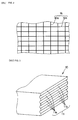
Fig. 2 is a plan view of a boundary-defining conductive pattern (first embodiment). -
Fig. 3 is a perspective view of a section of a multilayer ceramic substrate (first embodiment). -
Fig. 4 is a graph showing shrinkage rates (first embodiment). -
Fig. 5 is a cross-sectional view of a multilayer ceramic substrate (first alternative embodiment). -
Fig. 6 is a plan view of a boundary-defining conductive pattern (second alternative embodiment). -
Figs. 7(a) to 7(d) are cross-sectional views illustrating a production process of multilayer ceramic substrates (second embodiment). -
- 10 multilayer ceramic substrate
- 11 section
- 11a ceramic-layer-break portion
- 11b cavity-separation portion
- 12a green ceramic laminate
- 12b sintered ceramic laminate
- 14 in-plane conductive pattern (conductive pattern)
- 15 conductive via pattern (conductive pattern)
- 16, 16a, 16b boundary-defining conductive pattern (conductive pattern)
- 18a, 18b cavity
- 20, 22 shrinkage inhibiting green sheet
- 50 green ceramic laminate
- 52 sintered ceramic laminate
- 52a, 52b piece
- 54 in-plane conductive pattern (boundary-defining conductive pattern)
- 56 cavity
- 58a, 58b section
- Embodiments of the present invention will be described below with reference to
Figs. 1 to 7 . - A method for producing a multilayer ceramic substrate according to a first embodiment will be described below with reference to
Figs. 1 to 4 . - A brief outline of the method for producing a multilayer ceramic substrate will be described below with reference to
Fig. 1 which is a cross-sectional view. - As shown in
Fig. 1(a) , shrinkage inhibitinggreen sheets - The green ceramic laminate 12a includes in-plane
conductive patterns 14 to be formed into internal electrodes, internal leads, embedded elements, and the like in the multilayer ceramic substrates, the in-planeconductive patterns 14 being arranged between a plurality of stacked ceramicgreen sheets 13; and boundary-definingconductive patterns 16 arranged along boundaries among the multilayer ceramic substrates. As shown inFig. 2 which is a plan view viewed in the stacking direction of the ceramicgreen sheets 13, the boundary-definingconductive patterns 16 each includesegments 16a extending longitudinally andsegments 16b extending laterally, thesegments - Conductive via
patterns 15 passing through the ceramicgreen sheets 13 and connected to the in-planeconductive patterns 14 are formed in the ceramicgreen sheets 13. - The shrinkage behavior of the ceramic
green sheets 13 and the shrinkage behavior of the in-planeconductive patterns 14 are adjusted in such a manner that a cavity is not formed between the ceramic layers during firing. The boundary-definingconductive patterns 16 is composed of a material such that the sintering behavior thereof when the green ceramic laminate 12a is fired is significantly different from the sintering behavior of the ceramicgreen sheets 13. The boundary-defining thick-film patterns are preferably conductive patterns mainly composed of a conductive material such as Ag or Cu. Alternatively, the boundary-defining thick-film patterns may be an insulating patterns mainly composed of an insulating material such as a ceramic material or glass. - As schematically shown in
Fig. 1(b) ,cavities conductive pattern 16 in a firedceramic laminate 12b. That is, the ceramic layers that sandwich the boundary-definingconductive patterns 16 shrink in the vicinity of the outer edges of the boundary-definingconductive patterns 16 due to the contact with the boundary-definingconductive patterns 16. Thereby, thecavities Fig. 1(b) shows a state after the removal of the shrinkage inhibiting layers. - For example, the boundary-defining
conductive patterns 16 are formed of a Ag paste having a shrinkage rate higher than those of the ceramicgreen sheets 13 during sintering by heat. In this case, the amount of shrinkage of each boundary-definingconductive pattern 16 is larger than that of the ceramic green sheets arranged around thepattern 16. Thus, thecavities conductive pattern 16. - Alternatively, the boundary-defining
conductive patterns 16 are formed of a Ag paste having a sintering initiation temperature lower than that of each ceramicgreen sheet 13. In this case, the boundary-definingconductive patterns 16 begin to shrink earlier than the ceramic green sheets around thepatterns 16. Thus, thecavities conductive pattern 16. - The fired
ceramic laminate 12b can be divided by bending intopieces cavities Fig. 1(c) . - As shown in
Fig. 3 , cavity-separation portions 11b formed by dividing thecavities break portions 11a formed by breakage of the ceramic layers are exposed atsection 11 of each of thepieces separation portions 11b. Grain boundary failure and intragranular failure occur at theelectric signal 11a. - To promote the initiation of separation, one or more grooves may be formed in either or both main surfaces of the green ceramic laminate 12a.
- An example of the production of the multilayer ceramic substrates will be described below.
- Ceramic green sheets containing ceramic materials are prepared.
- Specifically, the ceramic green sheets are produced as follows: A mixture of 50 to 65 percent by weight of a glass powder having a composition of CaO (10% to 55%), SiO2 (45% to 70%), Al2O3 (0% to 30% by weight), impurities (0% to 10% by weight), and B2O3 (0% to 20% by weight) and 35 to 50 percent by weight of an Al2O3 powder containing 0% to 10% by weight impurities is dispersed in an organic vehicle including an organic solvent, a plasticizer, and the like to prepare a slurry. The resulting slurry is formed into sheets by a doctor blade method or casting. Thereby, green glass ceramic layers (ceramic green sheets) are produced.
- The green glass ceramic layers (ceramic green sheets) are preferably ceramic green sheets formed by the above-described sheet-forming method. Alternatively, the green glass ceramic layers may be green thick printed layers. With respect to the ceramic powder, a magnetic material, such as ferrite, and a dielectric material, such as barium titanate, may be used as well as the above-described insulating material. As the ceramic green sheets, low-temperature co-fired ceramic green sheets that are sintered at 1,050°C or lower are preferred. Thus, the above-described glass powder has a softening point of 750°C or lower.
- Vias are formed in the green glass ceramic layers by punching or the like. Examples of a method for forming the in-plane
conductive patterns 14 include a method in which a conductive paste is applied by screen printing, gravure printing, or the like, and a method in which metal foil having a predetermined shape is transferred. - As the conductive material, a material mainly composed of Ag having low resistivity and oxidation resistance is preferred. In particular, when a higher bond strength to a ceramic material is required, at least one additive, such as Al2O3, may be incorporated in addition to Ag as a main component.
- The conductive paste may be produced by adding a predetermined proportion of an organic vehicle to the above-described the main component powder, and stirring and kneading the mixture. However, the sequence of mixing the main component powder, the additive powder, the organic vehicle, and the like is not particularly limited.
- The organic vehicle is a mixture of a binder resin and a solvent. Examples of the binder resin that can be used include ethyl cellulose, acrylic resins, polyvinyl butyral, and methacrylic resins.
- Examples of the solvent that can be used include terpineol, dihydroterpineol, dihydroterpineol acetate, butyl carbitol, butyl carbitol acetate, and alcohols.
- As needed, various dispersants, plasticizers, activators may be incorporated.
- The conductive paste preferably has a viscosity of 50 to 700 Pa·s in view of printability.
- The conductive patterns arranged on the surface includes portions where the conductive via
patterns 15, such as via-hole conductors and through-hole conductors, for connection of conductive patterns arranged different interfaces among the layers are exposed at the surface. The conductive viapatterns 15 are formed by filling the above-described paste into the through holes, which are formed in the glass ceramic green sheets by punching or the like, by printing or the like. - A paste for forming the boundary-defining
conductive patterns 16 is formed and applied by printing as well as the paste for forming the in-planeconductive patterns 14. Preferably, with respect to a Ag powder mainly constituting the paste, coarse particles and extremely aggregated particles are not contained therein. The conductive paste preferably has a maximum particle size of 5 µm or less. - The shrinkage inhibiting green sheets are produced as follows: A powder of a ceramic material, such as alumina, which is not substantially sintered at a firing temperature of the above-described green glass ceramic layers (ceramic green sheets) is dispersed in an organic vehicle containing an organic binder, an organic solvent, a plasticizer, and the like to prepare a slurry. The resulting slurry is formed into sheets by a doctor blade method or casting. Thereby, the shrinkage inhibiting green sheets are produced. The shrinkage inhibiting green sheets are sintered at, for example, 1,400°C to 1,600°C and thus are not substantially sintered at the firing temperature of the green glass ceramic layers (ceramic green sheets).
- Each of the shrinkage inhibiting green sheets may have a single-layer structure or a structure including a plurality of stacked layers. The ceramic powder used for the shrinkage inhibiting green sheets preferably has an average particle size of 0.1 to 5.0 µm. In the case of the ceramic powder having an average particle size of less than 0.1 µm, the powder reacts vigorously with the glass components contained in the vicinity of surfaces of the green glass ceramic layers; hence, in some cases, the glass ceramic layers are bonded to the shrinkage inhibiting green sheets after firing. As a result, the shrinkage inhibiting green sheets cannot be removed. Furthermore, delamination may occur in the substrate because the organic components, such as the binder, in the sheets are not easily eliminated due to such a small particle size. On the other hand, the ceramic powder having an average particle size exceeding 5.0 µm tends to have a reduced inhibiting power to inhibit firing shrinkage, thereby causing the substrate to shrink unnecessarily in the x and y directions or to warp.
- The ceramic powder constituting the shrinkage inhibiting green sheets may be a ceramic powder that is not substantially sintered at the firing temperature of the green glass ceramic layers. Ceramic powders such as zirconia and magnesia may be used as well as alumina. However, to increase the amount of the glass components in surface regions of the green glass ceramic layers, the glass components in the surfaces need to have good wettability for the shrinkage inhibiting green sheets at interfaces where the surfaces are in contact with the shrinkage inhibiting green sheets. Thus, the same ceramic powder as the ceramic powder constituting the green glass ceramic layers is preferred.
- The ceramic green sheets including the in-plane conductive patterns, the conductive via patterns, and the boundary-defining conductive patterns are stacked to form a green ceramic laminate. A composite laminate including the shrinkage inhibiting green sheets arranged on both main surfaces of the ceramic laminate is produced by superposing the shrinkage inhibiting green sheets on one main surface and the other main surface of the green ceramic laminate and press-bonding the resulting article by isostatic pressing at a pressure of, for example, 5 to 200 MPa.
- Preferably, each of the shrinkage inhibiting green sheets has a thickness of 25 to 500 µm. The shrinkage inhibiting green sheets each having a thickness of less than 25 µm have a reduced inhibiting power to inhibit firing shrinkage, thereby allowing the substrate to shrink unnecessarily in the x and y directions or to warp, in some cases. At a thickness exceeding 500 µm, delamination tends to occur in the substrate because the organic components, such as the binder, in the sheets are not easily eliminated.
- The composite laminate is fired with a known belt furnace or a batch furnace at a firing temperature, e.g., 850°C to 950°C, of the ceramic green sheets of the ceramic laminate to sinter the ceramic laminate. In this case, the green ceramic laminate shrinks significantly in the thickness direction but does not substantially shrink in the planar direction owing to the restraint effect of the shrinkage inhibiting green sheets.
- The shrinkage inhibiting green sheets are removed from the composite laminate after firing to obtain the sintered ceramic laminate including portions to be formed into the plurality of multilayer ceramic substrates.
- In the sintered composite laminate, the shrinkage inhibiting green sheets are not substantially sintered. The organic components contained therein before firing are eliminated. As a result, the shrinkage inhibiting green sheets become porous. Thus, the shrinkage inhibiting green sheets can be easily removed by sand blasting, wet blasting, a supersonic vibration technique, or the like.
- The ceramic laminate obtained by removing the shrinkage inhibiting green sheets is divided along the boundaries of the multilayer ceramic substrates into the pieces of the multilayer ceramic substrates.
- When the ceramic laminate is divided after firing, the stress concentration occurs in the vicinity of the cavities formed along the boundaries among the multilayer ceramic substrates to form cracks, resulting in the multilayer ceramic substrates each having target dimensions and smooth sections. The sections may be further smoothed by a smoothing process, such as barrel polishing.
-
Fig. 4 is a graph showing the TMA measurement results of the Ag pastes used for forming the boundary-defining conductive patterns and a glass-ceramic base material used for the ceramic green sheets. The graph clearly demonstrates great differences in shrinkage timing and the shrinkage rates. - The shrinkage curve, indicated by a solid line, of the glass-ceramic base material lies at an intermediate position between the Ag pastes having Ag particle sizes of 3 µm and 6 µm. The Ag paste having a particle size of 3 µm, indicated by a two-dot chain line, has a shrinkage initiation temperature lower than that of the glass-ceramic base material indicated by the solid line and a shrinkage rate higher than that of the Ag paste having a particle size of 6 µm.
- In the case where the Ag paste having a particle size of 3 µm is used for forming the boundary-defining conductive patterns, cavities are formed in the vicinity of interfaces among the boundary-defining conductive patterns and the ceramic layers after firing. On the other hand, in the case where the Ag paste having a particle size of 6 µm is used for forming the boundary-defining conductive patterns, cavities are not formed in the vicinity of interfaces among the boundary-defining conductive patterns and the ceramic layers after firing. Accordingly, the results demonstrate that the Ag paste used for forming the boundary-defining conductive patterns preferably has a particle size of 4 to 5 µm.
- The shrinkage behavior of the Ag paste varies not only depending on the Ag particle size but also, for example, the Ag content of the paste and the impurity content other than Ag. Specifically, the paste may have a Ag content of 85 percent by weight or less. The paste may contain 0.5 percent by weight or more of Al2O3 as an impurity.
- The presence and size of the cavities formed at the sides of each boundary-defining conductive pattern can be controlled by utilizing differences between the boundary-defining thick-film patterns and the ceramic green sheets in the shrinkage initiation temperature, the shrinkage termination temperature, and the shrinkage rate. For example, the presence and size of the cavities formed at the sides of each boundary-defining conductive pattern can be controlled by appropriately selecting the Ag particle size, particle-size distribution, shape (sphere, flat, etc.), and specific surface area in the Ag paste used for forming the boundary-defining conductive patterns. The presence and size of the cavities formed at the sides of each boundary-defining conductive pattern can also be controlled by appropriately selecting the particle size, particle-size distribution, shape, specific surface area, and material, of an additive, the presence of coating (surface state of Ag), a binder, a solvent, and the like.
- The ceramic laminate is separated at a section through one of the cavities formed at both sides of each boundary-defining conductive pattern. To form the section more accurately, as shown in
Fig. 5 which is a cross-sectional view, the positions and widths of the boundary-definingconductive patterns conductive patterns section 11s passing through thecavities 18 formed at thesides conductive patterns - The boundary-defining conductive patterns may also be arranged both sides of the section. Alternatively, the boundary-defining conductive patterns may overlap the in-plane conductive patterns.
- As shown in
Fig. 6 , boundary-definingconductive pattern segments - The boundary-defining conductive patterns may be formed part of the boundaries in place of the formation of boundary-defining
conductive pattern segments Figs. 2 and6 . For example, the boundary-defining conductive patterns may be formed longitudinally or laterally. In this case, the source substrate can be separated into strips. - As shown in
Fig. 7 which is a cross-sectional view, the boundary-defining conductive patterns may be formed so as to function also as the in-plane conductive patterns constituting the internal electrodes, leads, embedded elements, and the like. - In this case, as shown in
Fig. 7(a) , a greenceramic laminate 50 is formed in such a manner thatindividual sides 55 of in-plane conductive patterns 54 (e.g., internal electrodes of a capacitor) arranged between ceramicgreen sheets 51 are aligned along boundaries of multilayer ceramic substrates. The in-planeconductive patterns 54 are composed of a material having firing shrinkage behavior different from that of the ceramicgreen sheets 51, as in the first embodiment. The shrinkage inhibitinggreen sheets ceramic laminate 50, as in the first embodiment. - Firing is performed at a temperature at which the ceramic
green sheets 51 are sintered but the shrinkage inhibitinggreen sheets Fig. 7(b) ,cavities 56 are formed in the sinteredceramic laminate 52 and are adjacent tosides 55 of the in-planeconductive patterns 54 which are aligned. - As shown in
Fig. 7(c) , the shrinkage inhibitinggreen sheets - As shown in
Fig. 7(d) , the sintered ceramic laminate 52 (source substrate) is separated by bending intoportions 52b having sections cavities 56. External electrodes may be formed so as to be connected to end faces of the in-plane conductive patterns exposed at a side face. In the case where the external electrodes are not required, an insulating protective film may be formed. - As described above, when the boundary-defining conductive patterns formed by printing on the ceramic green sheets have sintering shrinkage behavior different from that of the ceramic green sheets during firing, the cavities adjacent to individual edges of the boundary-defining conductive patterns in the ceramic laminate are formed after firing. It is possible to form the cavities in the multilayer ceramic substrate without the formation of a groove or cavity in the ceramic green sheets before firing and without additional processing of forming a separation groove in the ceramic laminate after firing. In the case where the boundary-defining conductive patterns are formed on the front or back surface of the multilayer ceramic substrate, grooves are formed on the front or back surface of the multilayer ceramic substrate and are adjacent to individual edges of the boundary-defining conductive patterns.
- When the source substrate is bent, cracks passing through the cavities or grooves where the cross sectional thickness is reduced are formed, thus forming the sections passing through the cavities or grooves. Therefore, the source substrate can be divided accurately and easily into individual substrates. Hence, many circuit boards can be obtained from the single substrate.
- The boundary-defining conductive patterns may be formed on the ceramic green sheets in a step of forming the conductive patterns such as the internal electrodes and lead patterns. Thus, this eliminates the need to form a groove or a cavity, in advance, in the ceramic green sheets before firing or the ceramic laminate before firing. After firing, the ceramic laminate can be separated by bending. Thus, this eliminates the need for the processing of the ceramic laminate with a special cutting apparatus for cutting the hard ceramic laminate after firing (e.g., a laser beam machine, a dicing saw, or the like), thereby simplifying the process.
- Also in the case where the number of stacked ceramic layers is increased, sections can be accurately made by aligning the cavities in the stacking direction, thereby accurately and easily producing the multilayer ceramic substrate with high dimensional accuracy.
- The present invention is not limited to the above-described embodiments. Various changes may be made.
Claims (10)
- A method for producing a multilayer ceramic substrate, comprising:a first step of forming a green ceramic laminate including a plurality of stacked green ceramic layers;a second step of firing the green ceramic laminate to sinter the green ceramic layers; anda third step of dividing the sintered ceramic laminate formed by firing the green ceramic laminate into a plurality of pieces,wherein the green ceramic laminate formed in the first step includes at least one green boundary-defining thick-film pattern arranged on one main surface of at least one of the green ceramic layers and along a portion corresponding to the boundary between the pieces of the sintered ceramic laminate divided in the third step, the at least one green boundary-defining thick-film pattern having firing behavior different from that of the green ceramic layers adjacent to the at least one green boundary-defining thick-film pattern,
in the second step, a cavity is formed on the basis of the difference in firing shrinkage behavior between the at least one boundary-defining thick-film pattern and the ceramic layers in contact with the at least one boundary-defining thick-film pattern, the cavity being adjacent to at least part of an outer edge of the at least one boundary-defining thick-film pattern when viewed in the stacking direction of the ceramic layers, and
in the third step, the sintered ceramic laminate is divided along the cavity into the plurality of pieces. - The method for producing a multilayer ceramic substrate according to claim 1, wherein the firing shrinkage initiation temperature of the at least one green boundary-defining thick-film pattern is lower than those of the green ceramic layers in contact with the boundary-defining thick-film pattern.
- The method for producing a multilayer ceramic substrate according to claim 1 or 2, wherein the firing shrinkage rate of the at least one green boundary-defining thick-film pattern is higher than those of the ceramic layers in contact with the at least one boundary-defining thick-film pattern.
- The method for producing a multilayer ceramic substrate according to claim 1, 2, or 3,
wherein the at least one boundary-defining thick-film pattern comprises a plurality of boundary-defining thick-film patterns, wherein the boundary-defining thick-film patterns are arranged at different interfaces among the green ceramic layers, and at least part of an outer edge of each of the boundary-defining thick-film patterns is arranged in a common imaginary plane extending in the stacking direction of the green ceramic layers. - The method for producing a multilayer ceramic substrate according to any one of claims 1 to 4,
wherein the first step includes a substep of bringing a green shrinkage inhibiting layer that is not substantially sintered at a firing temperature of the green ceramic layers into close contact with at least one main surface of the green ceramic laminate,
in the second step, the green ceramic laminate in close contact with the shrinkage inhibiting layer is fired at a temperature from a sintering temperature of the ceramic layers to a temperature at which the shrinkage inhibiting layer is not substantially sintered, and
the method further comprises a step of removing the shrinkage inhibiting layer in close contact with the sintered ceramic laminate between the second step and the third step. - The method for producing a multilayer ceramic substrate according to any one of claims 1 to 5, wherein the at least one green boundary-defining thick-film pattern is a green boundary-defining conductive pattern containing a conductive material.
- The method for producing a multilayer ceramic substrate according to claim 6, wherein the sintered ceramic laminate includes an internal circuit conductive pattern constituting an embedded element arranged between the ceramic layers, and
wherein the internal circuit conductive pattern is electrically remote from the boundary-defining conductive pattern. - The method for producing a multilayer ceramic substrate according to claim 6, wherein at least part of the boundary-defining conductive pattern constitutes an embedded element arranged between the ceramic layers of the sintered ceramic laminate.
- The method for producing a multilayer ceramic substrate according to any one of claims 1 to 8, further comprising a step of mounting a surface-mounted electronic component on the sintered ceramic laminate before or after the sintered ceramic laminate is divided into the plurality of pieces.
- A source substrate of multilayer ceramic substrates, comprising a plurality of ceramic layers bonded to each other, a conductive pattern arranged at at least one interface among the ceramic layers, and portions to be formed into a plurality of multilayer ceramic substrates,
wherein when the source substrate is viewed in the stacking direction of the ceramic layers, a cavity is formed at a boundary of the multilayer ceramic substrates, the cavity being adjacent to at least part of an outer edge of the conductive pattern.
Applications Claiming Priority (2)
| Application Number | Priority Date | Filing Date | Title |
|---|---|---|---|
| JP2006148246 | 2006-05-29 | ||
| PCT/JP2007/059612 WO2007138826A1 (en) | 2006-05-29 | 2007-05-09 | Method for manufacturing ceramic multilayer substrate |
Publications (3)
| Publication Number | Publication Date |
|---|---|
| EP2023701A1 true EP2023701A1 (en) | 2009-02-11 |
| EP2023701A4 EP2023701A4 (en) | 2009-05-20 |
| EP2023701B1 EP2023701B1 (en) | 2010-12-08 |
Family
ID=38778346
Family Applications (1)
| Application Number | Title | Priority Date | Filing Date |
|---|---|---|---|
| EP07743047A Not-in-force EP2023701B1 (en) | 2006-05-29 | 2007-05-09 | Method for manufacturing ceramic multilayer substrate |
Country Status (8)
| Country | Link |
|---|---|
| US (1) | US8105453B2 (en) |
| EP (1) | EP2023701B1 (en) |
| JP (1) | JP4803185B2 (en) |
| KR (1) | KR100989342B1 (en) |
| CN (1) | CN101341808B (en) |
| AT (1) | ATE491327T1 (en) |
| DE (1) | DE602007011058D1 (en) |
| WO (1) | WO2007138826A1 (en) |
Cited By (2)
| Publication number | Priority date | Publication date | Assignee | Title |
|---|---|---|---|---|
| EP2051570A4 (en) * | 2006-08-07 | 2009-11-25 | Murata Manufacturing Co | Method of producing multilayer ceramic substrate |
| US9524826B2 (en) | 2014-04-21 | 2016-12-20 | Samsung Electro-Mechanics Co., Ltd. | Multilayer ceramic capacitor and method of manufacturing the same |
Families Citing this family (23)
| Publication number | Priority date | Publication date | Assignee | Title |
|---|---|---|---|---|
| KR100887127B1 (en) * | 2007-11-23 | 2009-03-04 | 삼성전기주식회사 | Manufacturing method of multilayer ceramic substrate |
| JP4497247B2 (en) * | 2008-02-19 | 2010-07-07 | 株式会社村田製作所 | Manufacturing method of multilayer ceramic electronic component |
| KR101018102B1 (en) * | 2008-08-25 | 2011-02-25 | 삼성전기주식회사 | Multilayer LTC Substrate and Manufacturing Method Thereof |
| DE102008046336A1 (en) * | 2008-09-09 | 2010-03-11 | Osram Gesellschaft mit beschränkter Haftung | LTCC layer stack |
| JP2010245088A (en) * | 2009-04-01 | 2010-10-28 | Murata Mfg Co Ltd | Method for manufacturing multilayer ceramic electronic component |
| JP5673064B2 (en) * | 2010-12-15 | 2015-02-18 | 株式会社村田製作所 | Method for manufacturing a coil-embedded substrate |
| CA2823578C (en) | 2010-12-30 | 2016-09-20 | Saint-Gobain Abrasives, Inc. | Coated abrasive aggregates and products containing same |
| JP5921074B2 (en) * | 2011-03-17 | 2016-05-24 | 株式会社村田製作所 | Manufacturing method of laminated substrate |
| JP5945099B2 (en) | 2011-04-20 | 2016-07-05 | 日本特殊陶業株式会社 | Wiring board, multi-cavity wiring board, and manufacturing method thereof |
| KR20140075718A (en) | 2011-09-29 | 2014-06-19 | 생-고뱅 어브레이시브즈, 인코포레이티드 | Abrasive products and methods for finishing hard surfaces |
| WO2013057867A1 (en) * | 2011-10-21 | 2013-04-25 | パナソニック株式会社 | Semiconductor device |
| JP4999029B1 (en) * | 2011-11-11 | 2012-08-15 | 株式会社Maruwa | Cut and sintered ceramic sheet and manufacturing method thereof |
| JP5682548B2 (en) * | 2011-12-14 | 2015-03-11 | 株式会社村田製作所 | Multilayer inductor element and manufacturing method thereof |
| US9321947B2 (en) | 2012-01-10 | 2016-04-26 | Saint-Gobain Abrasives, Inc. | Abrasive products and methods for finishing coated surfaces |
| WO2013138765A1 (en) | 2012-03-16 | 2013-09-19 | Saint-Gobain Abrasives, Inc. | Abrasive products and methods for finishing surfaces |
| WO2013149197A1 (en) | 2012-03-30 | 2013-10-03 | Saint-Gobain Abrasives, Inc. | Abrasive products and methods for fine polishing of ophthalmic lenses |
| TW201440983A (en) * | 2013-04-24 | 2014-11-01 | 蔚華科技股份有限公司 | Method for manufacturing miniature passive components |
| KR101490760B1 (en) * | 2013-07-04 | 2015-02-11 | 에스케이씨 주식회사 | Cut-out laminated sheet and preparation method thereof |
| US9724897B2 (en) * | 2015-01-07 | 2017-08-08 | Emisense Technologies, Llc | Processing method for constraining lower melting point metals within ceramic laminates during sintering |
| CN105098300A (en) * | 2015-09-11 | 2015-11-25 | 禾邦电子(中国)有限公司 | Common-mode filter and manufacturing method therefor |
| DE112017003656B4 (en) * | 2016-07-21 | 2025-01-30 | Ngk Insulators, Ltd. | manufacturing process for sensor element |
| JP7180619B2 (en) * | 2020-01-10 | 2022-11-30 | Tdk株式会社 | Electronic parts and manufacturing methods thereof |
| TWI775280B (en) * | 2021-01-20 | 2022-08-21 | 力晶積成電子製造股份有限公司 | Capacitor integrated structure, capacitor unit and manufacturing method thereof |
Family Cites Families (21)
| Publication number | Priority date | Publication date | Assignee | Title |
|---|---|---|---|---|
| US4353957A (en) * | 1973-09-24 | 1982-10-12 | Tam Ceramics Inc. | Ceramic matrices for electronic devices and process for forming same |
| JPS6252917A (en) * | 1985-08-30 | 1987-03-07 | 株式会社村田製作所 | Manufacture of single-plate capacitor |
| JPH0438071U (en) | 1990-07-27 | 1992-03-31 | ||
| JPH0575262A (en) | 1991-09-11 | 1993-03-26 | Matsushita Electric Ind Co Ltd | Manufacture of ceramic multilayer circuit board |
| EP0582881B1 (en) * | 1992-07-27 | 1997-12-29 | Murata Manufacturing Co., Ltd. | Multilayer electronic component, method of manufacturing the same and method of measuring characteristics thereof |
| JPH0685460A (en) * | 1992-09-07 | 1994-03-25 | Fujitsu Ltd | Manufacture of ceramic multilayer board |
| JP3330104B2 (en) * | 1999-07-29 | 2002-09-30 | 京セラ株式会社 | Manufacturing method of multi-cavity ceramic wiring board |
| JP2001332857A (en) * | 2000-05-22 | 2001-11-30 | Kyocera Corp | Manufacturing method of wiring board |
| JP2002016359A (en) * | 2000-06-27 | 2002-01-18 | Kyocera Corp | Manufacturing method of wiring board |
| JP3785903B2 (en) | 2000-07-21 | 2006-06-14 | 株式会社村田製作所 | Multilayer substrate and manufacturing method thereof |
| JP2002226259A (en) * | 2000-11-29 | 2002-08-14 | Murata Mfg Co Ltd | Composition for base of ceramic electronic component, ceramic electronic component, and method for producing multilayer ceramic electronic component |
| JP2002270459A (en) | 2001-03-06 | 2002-09-20 | Taiyo Yuden Co Ltd | Manufacturing method for laminated ceramic electronic component |
| JP2003017851A (en) * | 2001-06-29 | 2003-01-17 | Murata Mfg Co Ltd | Method for manufacturing multilayer ceramic substrate |
| JP2003246680A (en) * | 2002-02-26 | 2003-09-02 | Murata Mfg Co Ltd | Method for manufacturing multilayer ceramic substrate |
| WO2005039263A1 (en) * | 2003-10-17 | 2005-04-28 | Hitachi Metals, Ltd. | Multi-layer ceramic substrate, method for manufacturng the same and electronic device using the same |
| JP4470158B2 (en) * | 2003-10-24 | 2010-06-02 | 日立金属株式会社 | Multilayer ceramic substrate manufacturing method and multilayer ceramic substrate |
| JP3908715B2 (en) * | 2003-10-24 | 2007-04-25 | Tdk株式会社 | Multilayer ceramic capacitor |
| JP4291187B2 (en) * | 2004-03-24 | 2009-07-08 | Tdk株式会社 | Method for forming external electrode built-in layer and method for manufacturing multilayer electronic component using the same |
| JP2005229135A (en) * | 2005-04-22 | 2005-08-25 | Ngk Spark Plug Co Ltd | Ceramic wiring board and method for manufacturing the same |
| JP2006245592A (en) * | 2006-03-20 | 2006-09-14 | Kyocera Corp | Wiring board |
| DE602007011286D1 (en) * | 2006-08-07 | 2011-01-27 | Murata Manufacturing Co | METHOD FOR PRODUCING A CERAMIC, MULTILAYER SUBSTRATE |
-
2007
- 2007-05-09 DE DE602007011058T patent/DE602007011058D1/en active Active
- 2007-05-09 JP JP2007556188A patent/JP4803185B2/en not_active Expired - Fee Related
- 2007-05-09 EP EP07743047A patent/EP2023701B1/en not_active Not-in-force
- 2007-05-09 KR KR1020087004099A patent/KR100989342B1/en not_active Expired - Fee Related
- 2007-05-09 WO PCT/JP2007/059612 patent/WO2007138826A1/en not_active Ceased
- 2007-05-09 CN CN2007800008637A patent/CN101341808B/en not_active Expired - Fee Related
- 2007-05-09 AT AT07743047T patent/ATE491327T1/en not_active IP Right Cessation
-
2008
- 2008-02-12 US US12/029,545 patent/US8105453B2/en not_active Expired - Fee Related
Cited By (3)
| Publication number | Priority date | Publication date | Assignee | Title |
|---|---|---|---|---|
| EP2051570A4 (en) * | 2006-08-07 | 2009-11-25 | Murata Manufacturing Co | Method of producing multilayer ceramic substrate |
| US7833370B2 (en) | 2006-08-07 | 2010-11-16 | Murata Manufacturing Co., Ltd. | Method for manufacturing a ceramic multi-layered substrate |
| US9524826B2 (en) | 2014-04-21 | 2016-12-20 | Samsung Electro-Mechanics Co., Ltd. | Multilayer ceramic capacitor and method of manufacturing the same |
Also Published As
| Publication number | Publication date |
|---|---|
| US20080135155A1 (en) | 2008-06-12 |
| KR20080033996A (en) | 2008-04-17 |
| EP2023701B1 (en) | 2010-12-08 |
| CN101341808B (en) | 2010-06-23 |
| WO2007138826A1 (en) | 2007-12-06 |
| US8105453B2 (en) | 2012-01-31 |
| KR100989342B1 (en) | 2010-10-25 |
| EP2023701A4 (en) | 2009-05-20 |
| JP4803185B2 (en) | 2011-10-26 |
| CN101341808A (en) | 2009-01-07 |
| JPWO2007138826A1 (en) | 2009-10-01 |
| DE602007011058D1 (en) | 2011-01-20 |
| ATE491327T1 (en) | 2010-12-15 |
Similar Documents
| Publication | Publication Date | Title |
|---|---|---|
| EP2023701B1 (en) | Method for manufacturing ceramic multilayer substrate | |
| EP2051570B1 (en) | Method of producing multilayer ceramic substrate | |
| JP3716832B2 (en) | Method for producing ceramic multilayer substrate and unfired composite laminate | |
| CN1229209C (en) | Method for producing ceramic multilayer substrate and unfired composite laminate | |
| JP2003110238A (en) | Manufacturing method of glass ceramic multilayer substrate | |
| EP2325150A1 (en) | Low temperature co-fired ceramic material, low temperature co-fired ceramic body, and multilayer ceramic substrate | |
| EP1189495B1 (en) | Method of manufacturing multilayer ceramic substrate | |
| JP2007221115A (en) | Manufacturing method of conductor paste and multilayer ceramic substrate | |
| JP4888564B2 (en) | Manufacturing method of ceramic multilayer substrate with cavity | |
| JP4084696B2 (en) | Low temperature fired multilayer ceramic wiring board manufacturing method | |
| JP2007258264A (en) | Assembled substrate, and manufacturing method of individual substrate | |
| JP4645962B2 (en) | Multilayer ceramic substrate | |
| JP2007053294A (en) | Process for manufacturing multilayer ceramic electronic component | |
| JP2005011843A (en) | Multilayered ceramic board and its manufacturing method | |
| JPH0828579B2 (en) | Method for manufacturing ceramic multilayer substrate | |
| JP2004063910A (en) | Manufacturing method of ceramic laminate |
Legal Events
| Date | Code | Title | Description |
|---|---|---|---|
| PUAI | Public reference made under article 153(3) epc to a published international application that has entered the european phase |
Free format text: ORIGINAL CODE: 0009012 |
|
| 17P | Request for examination filed |
Effective date: 20080122 |
|
| AK | Designated contracting states |
Kind code of ref document: A1 Designated state(s): AT BE BG CH CY CZ DE DK EE ES FI FR GB GR HU IE IS IT LI LT LU LV MC MT NL PL PT RO SE SI SK TR |
|
| AX | Request for extension of the european patent |
Extension state: AL BA HR MK RS |
|
| A4 | Supplementary search report drawn up and despatched |
Effective date: 20090420 |
|
| 17Q | First examination report despatched |
Effective date: 20091030 |
|
| GRAP | Despatch of communication of intention to grant a patent |
Free format text: ORIGINAL CODE: EPIDOSNIGR1 |
|
| DAX | Request for extension of the european patent (deleted) | ||
| GRAS | Grant fee paid |
Free format text: ORIGINAL CODE: EPIDOSNIGR3 |
|
| GRAA | (expected) grant |
Free format text: ORIGINAL CODE: 0009210 |
|
| AK | Designated contracting states |
Kind code of ref document: B1 Designated state(s): AT BE BG CH CY CZ DE DK EE ES FI FR GB GR HU IE IS IT LI LT LU LV MC MT NL PL PT RO SE SI SK TR |
|
| REG | Reference to a national code |
Ref country code: GB Ref legal event code: FG4D |
|
| REG | Reference to a national code |
Ref country code: CH Ref legal event code: EP |
|
| REG | Reference to a national code |
Ref country code: IE Ref legal event code: FG4D |
|
| REF | Corresponds to: |
Ref document number: 602007011058 Country of ref document: DE Date of ref document: 20110120 Kind code of ref document: P |
|
| REG | Reference to a national code |
Ref country code: NL Ref legal event code: VDEP Effective date: 20101208 |
|
| PG25 | Lapsed in a contracting state [announced via postgrant information from national office to epo] |
Ref country code: LT Free format text: LAPSE BECAUSE OF FAILURE TO SUBMIT A TRANSLATION OF THE DESCRIPTION OR TO PAY THE FEE WITHIN THE PRESCRIBED TIME-LIMIT Effective date: 20101208 |
|
| LTIE | Lt: invalidation of european patent or patent extension |
Effective date: 20101208 |
|
| PG25 | Lapsed in a contracting state [announced via postgrant information from national office to epo] |
Ref country code: LV Free format text: LAPSE BECAUSE OF FAILURE TO SUBMIT A TRANSLATION OF THE DESCRIPTION OR TO PAY THE FEE WITHIN THE PRESCRIBED TIME-LIMIT Effective date: 20101208 Ref country code: FI Free format text: LAPSE BECAUSE OF FAILURE TO SUBMIT A TRANSLATION OF THE DESCRIPTION OR TO PAY THE FEE WITHIN THE PRESCRIBED TIME-LIMIT Effective date: 20101208 Ref country code: NL Free format text: LAPSE BECAUSE OF FAILURE TO SUBMIT A TRANSLATION OF THE DESCRIPTION OR TO PAY THE FEE WITHIN THE PRESCRIBED TIME-LIMIT Effective date: 20101208 Ref country code: SI Free format text: LAPSE BECAUSE OF FAILURE TO SUBMIT A TRANSLATION OF THE DESCRIPTION OR TO PAY THE FEE WITHIN THE PRESCRIBED TIME-LIMIT Effective date: 20101208 Ref country code: AT Free format text: LAPSE BECAUSE OF FAILURE TO SUBMIT A TRANSLATION OF THE DESCRIPTION OR TO PAY THE FEE WITHIN THE PRESCRIBED TIME-LIMIT Effective date: 20101208 Ref country code: SE Free format text: LAPSE BECAUSE OF FAILURE TO SUBMIT A TRANSLATION OF THE DESCRIPTION OR TO PAY THE FEE WITHIN THE PRESCRIBED TIME-LIMIT Effective date: 20101208 Ref country code: CY Free format text: LAPSE BECAUSE OF FAILURE TO SUBMIT A TRANSLATION OF THE DESCRIPTION OR TO PAY THE FEE WITHIN THE PRESCRIBED TIME-LIMIT Effective date: 20101208 Ref country code: BG Free format text: LAPSE BECAUSE OF FAILURE TO SUBMIT A TRANSLATION OF THE DESCRIPTION OR TO PAY THE FEE WITHIN THE PRESCRIBED TIME-LIMIT Effective date: 20110308 |
|
| PG25 | Lapsed in a contracting state [announced via postgrant information from national office to epo] |
Ref country code: EE Free format text: LAPSE BECAUSE OF FAILURE TO SUBMIT A TRANSLATION OF THE DESCRIPTION OR TO PAY THE FEE WITHIN THE PRESCRIBED TIME-LIMIT Effective date: 20101208 Ref country code: GR Free format text: LAPSE BECAUSE OF FAILURE TO SUBMIT A TRANSLATION OF THE DESCRIPTION OR TO PAY THE FEE WITHIN THE PRESCRIBED TIME-LIMIT Effective date: 20110309 Ref country code: ES Free format text: LAPSE BECAUSE OF FAILURE TO SUBMIT A TRANSLATION OF THE DESCRIPTION OR TO PAY THE FEE WITHIN THE PRESCRIBED TIME-LIMIT Effective date: 20110319 Ref country code: IS Free format text: LAPSE BECAUSE OF FAILURE TO SUBMIT A TRANSLATION OF THE DESCRIPTION OR TO PAY THE FEE WITHIN THE PRESCRIBED TIME-LIMIT Effective date: 20110408 Ref country code: BE Free format text: LAPSE BECAUSE OF FAILURE TO SUBMIT A TRANSLATION OF THE DESCRIPTION OR TO PAY THE FEE WITHIN THE PRESCRIBED TIME-LIMIT Effective date: 20101208 Ref country code: PT Free format text: LAPSE BECAUSE OF FAILURE TO SUBMIT A TRANSLATION OF THE DESCRIPTION OR TO PAY THE FEE WITHIN THE PRESCRIBED TIME-LIMIT Effective date: 20110408 Ref country code: CZ Free format text: LAPSE BECAUSE OF FAILURE TO SUBMIT A TRANSLATION OF THE DESCRIPTION OR TO PAY THE FEE WITHIN THE PRESCRIBED TIME-LIMIT Effective date: 20101208 |
|
| PG25 | Lapsed in a contracting state [announced via postgrant information from national office to epo] |
Ref country code: PL Free format text: LAPSE BECAUSE OF FAILURE TO SUBMIT A TRANSLATION OF THE DESCRIPTION OR TO PAY THE FEE WITHIN THE PRESCRIBED TIME-LIMIT Effective date: 20101208 Ref country code: SK Free format text: LAPSE BECAUSE OF FAILURE TO SUBMIT A TRANSLATION OF THE DESCRIPTION OR TO PAY THE FEE WITHIN THE PRESCRIBED TIME-LIMIT Effective date: 20101208 Ref country code: RO Free format text: LAPSE BECAUSE OF FAILURE TO SUBMIT A TRANSLATION OF THE DESCRIPTION OR TO PAY THE FEE WITHIN THE PRESCRIBED TIME-LIMIT Effective date: 20101208 |
|
| PLBE | No opposition filed within time limit |
Free format text: ORIGINAL CODE: 0009261 |
|
| STAA | Information on the status of an ep patent application or granted ep patent |
Free format text: STATUS: NO OPPOSITION FILED WITHIN TIME LIMIT |
|
| PG25 | Lapsed in a contracting state [announced via postgrant information from national office to epo] |
Ref country code: DK Free format text: LAPSE BECAUSE OF FAILURE TO SUBMIT A TRANSLATION OF THE DESCRIPTION OR TO PAY THE FEE WITHIN THE PRESCRIBED TIME-LIMIT Effective date: 20101208 |
|
| 26N | No opposition filed |
Effective date: 20110909 |
|
| PG25 | Lapsed in a contracting state [announced via postgrant information from national office to epo] |
Ref country code: MT Free format text: LAPSE BECAUSE OF FAILURE TO SUBMIT A TRANSLATION OF THE DESCRIPTION OR TO PAY THE FEE WITHIN THE PRESCRIBED TIME-LIMIT Effective date: 20101208 Ref country code: MC Free format text: LAPSE BECAUSE OF NON-PAYMENT OF DUE FEES Effective date: 20110531 Ref country code: IT Free format text: LAPSE BECAUSE OF FAILURE TO SUBMIT A TRANSLATION OF THE DESCRIPTION OR TO PAY THE FEE WITHIN THE PRESCRIBED TIME-LIMIT Effective date: 20101208 |
|
| REG | Reference to a national code |
Ref country code: CH Ref legal event code: PL |
|
| REG | Reference to a national code |
Ref country code: DE Ref legal event code: R097 Ref document number: 602007011058 Country of ref document: DE Effective date: 20110909 |
|
| GBPC | Gb: european patent ceased through non-payment of renewal fee |
Effective date: 20110509 |
|
| PG25 | Lapsed in a contracting state [announced via postgrant information from national office to epo] |
Ref country code: LI Free format text: LAPSE BECAUSE OF NON-PAYMENT OF DUE FEES Effective date: 20110531 Ref country code: CH Free format text: LAPSE BECAUSE OF NON-PAYMENT OF DUE FEES Effective date: 20110531 |
|
| REG | Reference to a national code |
Ref country code: FR Ref legal event code: ST Effective date: 20120131 |
|
| REG | Reference to a national code |
Ref country code: IE Ref legal event code: MM4A |
|
| PG25 | Lapsed in a contracting state [announced via postgrant information from national office to epo] |
Ref country code: IE Free format text: LAPSE BECAUSE OF NON-PAYMENT OF DUE FEES Effective date: 20110509 Ref country code: FR Free format text: LAPSE BECAUSE OF NON-PAYMENT OF DUE FEES Effective date: 20110531 |
|
| PG25 | Lapsed in a contracting state [announced via postgrant information from national office to epo] |
Ref country code: GB Free format text: LAPSE BECAUSE OF NON-PAYMENT OF DUE FEES Effective date: 20110509 |
|
| PG25 | Lapsed in a contracting state [announced via postgrant information from national office to epo] |
Ref country code: LU Free format text: LAPSE BECAUSE OF NON-PAYMENT OF DUE FEES Effective date: 20110509 |
|
| PG25 | Lapsed in a contracting state [announced via postgrant information from national office to epo] |
Ref country code: TR Free format text: LAPSE BECAUSE OF FAILURE TO SUBMIT A TRANSLATION OF THE DESCRIPTION OR TO PAY THE FEE WITHIN THE PRESCRIBED TIME-LIMIT Effective date: 20101208 |
|
| PG25 | Lapsed in a contracting state [announced via postgrant information from national office to epo] |
Ref country code: HU Free format text: LAPSE BECAUSE OF FAILURE TO SUBMIT A TRANSLATION OF THE DESCRIPTION OR TO PAY THE FEE WITHIN THE PRESCRIBED TIME-LIMIT Effective date: 20101208 |
|
| PGFP | Annual fee paid to national office [announced via postgrant information from national office to epo] |
Ref country code: DE Payment date: 20200520 Year of fee payment: 14 |
|
| REG | Reference to a national code |
Ref country code: DE Ref legal event code: R119 Ref document number: 602007011058 Country of ref document: DE |
|
| PG25 | Lapsed in a contracting state [announced via postgrant information from national office to epo] |
Ref country code: DE Free format text: LAPSE BECAUSE OF NON-PAYMENT OF DUE FEES Effective date: 20211201 |