EP2018041B1 - Zeitbasierte digitale On-Chip-Konversion von Pixelausgaben - Google Patents
Zeitbasierte digitale On-Chip-Konversion von Pixelausgaben Download PDFInfo
- Publication number
- EP2018041B1 EP2018041B1 EP08160757.4A EP08160757A EP2018041B1 EP 2018041 B1 EP2018041 B1 EP 2018041B1 EP 08160757 A EP08160757 A EP 08160757A EP 2018041 B1 EP2018041 B1 EP 2018041B1
- Authority
- EP
- European Patent Office
- Prior art keywords
- ramp function
- time
- igl
- igr
- integration
- Prior art date
- Legal status (The legal status is an assumption and is not a legal conclusion. Google has not performed a legal analysis and makes no representation as to the accuracy of the status listed.)
- Active
Links
Images


Classifications
-
- G—PHYSICS
- G01—MEASURING; TESTING
- G01S—RADIO DIRECTION-FINDING; RADIO NAVIGATION; DETERMINING DISTANCE OR VELOCITY BY USE OF RADIO WAVES; LOCATING OR PRESENCE-DETECTING BY USE OF THE REFLECTION OR RERADIATION OF RADIO WAVES; ANALOGOUS ARRANGEMENTS USING OTHER WAVES
- G01S17/00—Systems using the reflection or reradiation of electromagnetic waves other than radio waves, e.g. lidar systems
- G01S17/88—Lidar systems specially adapted for specific applications
- G01S17/89—Lidar systems specially adapted for specific applications for mapping or imaging
- G01S17/894—3D imaging with simultaneous measurement of time-of-flight at a 2D array of receiver pixels, e.g. time-of-flight cameras or flash lidar
Definitions
- Time of flight (TOF) sensors typically utilize charge-coupled device (CCD) or complementary metal oxide semiconductor (CMOS) based technologies that are able to sample at high speed.
- CCD charge-coupled device
- CMOS complementary metal oxide semiconductor
- the typical application is for point distance sensing or three-dimensional (3D) imaging in which the scene of interest is actively illuminated with modulated illuminating radiation and the sensor sampling is performed synchronously with the modulation of the illuminating radiation.
- 3D three-dimensional
- German patent application DE19821974A1 (Schwarte, Vorplatz und Anlagen für für Ü Kunststoff Kunststoff Kunststoff Kunststoff Wellen, 1999), see also US Pat. No. 6,825,455 B1 , disclosed a photon-mixing element for a TOF sensor in which the switches that are used to transfer the charge carriers to the integration gates are controlled based on the modulation used for the illumination signal.
- a photon-mixing element for a TOF sensor in which the switches that are used to transfer the charge carriers to the integration gates are controlled based on the modulation used for the illumination signal.
- a combined structure of stripe-like elements, each of them with short transport paths is proposed. Nevertheless, the stripe-like structure leads to a poor fill-factor because the regions between the stripes are not photo-sensitive.
- WO 2007/045108 A1 presents a newer TOF sensor example.
- the drift field over most or all of the photosensitive area is basically static in time.
- the static or quasi static field in the photosensitive region moves or dumps the charge carriers into a typically smaller modulated region, which may or may not be photosensitive.
- the charge carriers are then swept from the modulated region into integration regions or gates synchronously with the modulated signal.
- This newer system can operate at much higher frequencies because demodulation is over a much smaller area, having a lower intrinsic capacitance, whereas transport within the large photosensitive region can be optimized for speed.
- the newer demodulation device avoids the trade-off between the sensitivity/fill-factor and the demodulation speed. Both aspects can be optimized in the pixel at the same time using this technology.
- the charge that is accumulated in the integration regions of each pixel must be read out. This readout typically happens in a readout stage.
- Two types of information are important. First the total amount of charge held in all of the integration regions of a pixel is important to generate the standard two-dimensional (2D) grayscale image of the scene (offset). Second, the difference in the amount of charge held in the integration regions is important to generate the 3D depth information and to generate the amplitude for each pixel.
- EP 1 777 811 A1 discloses a pixel in semiconductor technology comprises a photosensitive detection region for converting an electromagnetic wave field into an electric signal of flowing charges, a separated demodulation region with at least two output nodes and means for sampling the charge-current signal at at least two different time intervals within a modulation period.
- a contact node links the detection region to the demodulation region.
- a drift field accomplishes the transfer of the electric signal of flowing charges from the detection region to the contact node. The electric signal of flowing charges is then transferred from the contact node during each of the two time intervals to the two output nodes allocated to the respective time interval.
- WO 2005/120046 A2 discloses and imaging device comprising an array of pixels fabricated using a microelectronic technology such as CMOS.
- the imaging device provides information regarding rapid increases in incident radiation.
- the sensor is sensitive to a variable quantity to be imaged, such as visible or non-visible radiation, and a signal representative of the quantity is output. The quantity is measured over a monitoring period, and the timing of the incidence may also be output.
- the present invention concerned improved system and method for detecting the charge contained on the integration gates and also the difference in charge on the integration gates of each pixel. Instead of first shifting the charge from the integration gate to the sense node and then reading-out the analog value, the present system measures the time it takes from beginning of lowering the potential of the integration gate to when the charge starts flowing to the sense node.
- the output of the pixel is digital in the sense that there is no need to convert a certain amount of charge to an equivalent potential, but only show, when there was some charge flow from the integration gate.
- the sense node should be made as small as possible, thereby saving space in the pixel, while increasing the sensitivity of the sense node.
- both taps can be converted into a digital value without clipping the background illumination. Therefore a grayscale image is again available as it was not in other systems (e.g. WO2006010284A1 ).
- the resolution of the conversion can be easily adjusted by either increasing/decreasing the counter speed or by lowering the integration faster or slower respectively. It is even possible to adjust the resolution for the offset and the difference value separately by applying specific control functions to the integration gate.
- the present invention relates to an integrated sensor chip as set out in claim 1 and a read out method for an integrated sensor chip as set out in claim 10. Further embodiments are described in the dependent claims.
- phase delays between an optical illumination signal and an electronic reference signal are three-dimensional (3D) range measurement, fluorescence imaging, or optical communication.
- the acquisition of the distance information is accomplished by the measurement of the time-of-flight. That is the time the light needs for the round-trip from the measurement system, i.e., camera, to the object and back again to the system.
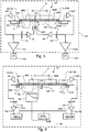
- Fig. 1 illustrates the basic principle of such a 3D-measurement camera system.
- Modulated illumination light ML 1 from an illumination module or light source IM is sent to the object OB of a scene.
- a fraction of the total optical power sent out is reflected to the camera 10 and detected by the image sensor SN.
- the sensor SN comprises a single pixel (point ranging) or a pixel matrix comprised of demodulation pixels DP. Each pixel DP is capable of demodulating the impinging light signal.
- a separate control board CB regulates the timing of the camera 100.
- the phase values of all pixels correspond to the particular distance information of one point in the scene. They are read out and displayed for example by a personal computer PC.
- Either pulse intensity-modulated or continuously intensity-modulated light is sent out by the illumination module or light source IM, reflected by the object and detected by the sensor. If each pixel of the sensor is capable of demodulating the optical signal at the same time, the sensor is able to deliver 3D images in real-time, i.e., frame rates of up to 30 Hertz (Hz), or even more, are possible. In pulse operation the demodulation would deliver the time-of-flight directly.
- Figs. 2A and 2B show the relationship between signals for the case of continuous sinusoidal modulation and the signal sampling. Although this specific modulation scheme is highlighted in the following, the utilization of the pixel in 3D-imaging is not restricted to this particular scheme. Any other modulation scheme is applicable: e.g. pulse, rectangular, pseudo-noise or chirp modulation. Only the final extraction of the distance information is different.
- Fig. 2A shows both the modulated emitted illumination signal ES and received signal RS.
- the amplitude A, offset B of the received signal RS and phase P between both signals are unknown, but they can be unambiguously reconstructed with at least three samples of the received signal.
- BG represents the received signal part due to background light.
- a sampling with four samples per modulation period is depicted.
- Each sample is an integration of the electrical signal over a duration dt that is a predefined fraction of the modulation period.
- the photo-generated charges are accumulated over several modulation periods, in some embodiments.
- the conduction channels of the demodulation region By activating the conduction channels of the demodulation region alternately the photogenerated charge injected into the demodulation region and spread out below the complete gate structure, is forced to drift or diffuse to the specific storage site.
- the alternation of the channel activation is done synchronously with the sampling frequency.
- the electronic timing circuit employing for example a field programmable gate array (FPGA), generates the signals for the synchronous channel activation in the demodulation stage.
- FPGA field programmable gate array
- injected charge carriers are moved to the corresponding integration region.
- A B
- two samples A0 and A 1 of the modulation signal sampled at times that differ by half of the modulation period allow the calculation of the phase P and the amplitude A of a sinusoidal intensity modulated current injected into the sampling stage.
- Fig. 3 shows prior art circuit as described in WO2006010284A1 for reading out the photogenerated charge stored in the integration regions of the demodulation pixel DP and specifically generate signals corresponding to the sum and difference of the photogenerated charge held in the integration regions of the demodulation pixel.
- Charge is swept from the modulation region M, which is either photo-sensitive or photo-insensitive, and gathers in left and right integration regions IRL, IRR, under respective left and right integration gates IGL, IGR.
- the illustrated system uses a three gate structure, a center, unmodulated, gate CG in combination with left and right modulated gates MGL, MGR in the modulation region M to sweep the charge into either integration region IRL, IRR under integration gates IGL, IGR.
- profile of the potential PP is raised on one modulation gate while be lowered on the other modulation gate in order to create a drift field that moves the charge laterally across the pixel P and into the corresponding integration gate.
- the dotted portions of the potential profile PP are applied during one phase within the period of the illumination radiation. These dotted portions indicate a low potential on the right modulation gate MGR and higher potential center gate CG and even higher potential on the left modulation gate MGL to move charge in modulation region M to the left integration region IRL under the left integration gate IGL.
- the potentials indicated by the solid lines of the potential profile PP are applied across the modulation region M.
- the solid portions of the potential profile PP indicate a low potential on the left modulation gate MGL and high potential on the right modulation gate MGR to move charge to the right integration region IRR under the right integration gate IGR.
- charges are collected in the integration regions IRL, IRR for one or several cycles of the stimulation or illumination radiation before readout of the pixel DP is initiated.
- the charge in the integration regions IRL, IRR is first shifted over outgates OUTGL, OUTGR, see arrow S, to an associated left sense node SNL and right sense node SNR, which are typically diffusions in the substrate W.
- the potentials of both modulation gates MGL, MGR are lowered to isolate the integration regions IRL, IRR from the modulation region M.
- the potentials of the integration gates IGL, IGR are continuously decreased (assuming electron charge carriers) by the integration gate voltage controller IGVC until both sense nodes SNL, SNR have received charge from under their associated integration gate IGL, IGR.
- the integration gates IGL, IGR potential is lowered in a linear fashion whereas in other commercial devices, the potential lowered initially at a high rate of change with rate of change then reduced and possibly linear.
- the control of the integration gates IGL, IGR is individual for each pixel since the potential is lowered on the integration gates IGL, IGR only until charge is received on both sense nodes SNL, SNR.
- left sense amplifier SAL and right sense amplifier SAR are responsive to the charge on the respective sense nodes SNL, SNR.
- Right and left timing capacitors CL, CR receive the voltage output from the left sense amplifier SAL and right sense amplifier SAR, respectively.
- the signals from the capacitors CL, CR is amplified by left and right amplifiers AL, AR and provided as inputs to the integration gate voltage controller IGVC. When both inputs go to logic high, the integration gate voltage controller IGVC stops lowering the potentials of both integration gates IGL, IGR.
- This system provides a signal output corresponding to the difference in the charges collected by the integration gates IGL, IGR. This difference is finally used for the calculation of phase P (see equation above).
- the background can be derived by reading out the voltage applied to integration gate at the time the integration gate decrease had been stopped.
- the combination of integration gates and sense nodes enables this sensor to be both sensitive, on one hand, and function under large variations in illumination, i.e., dynamic range, on the other hand.
- the integration gates IGL, IGR can be made large in order to contain a large number of photogenerated electrons as would result from observing a well-lit screen.
- the sense nodes SNL, SNR can be made smaller for increased sensitivity, because to avoid saturation they must only be able to contain an amount of charge represented by the difference between the charge contained in the two integration gates IGL, IGR.
- Fig. 4 shows a circuit for reading out the photogenerated charge stored in the integration regions of the demodulation pixel DP, which has been constructed according to the principles of the present invention. This circuit measures the time it takes from the beginning of the lowering the potential of the integration gates to when the charge starts flowing to the sense node.
- a ramp generator RG is used to generate function of decreasing potential that is applied in common to both integration gates IGL, IGR under control of a clock signal clk.
- a counter CTR also responds to the clock pulse clk to begin a count that is held in each of two registers REGL, REGR, associated with the two integration gates IGL, IGR, respectively.
- the decreasing potential applied to the integration gates IGL, IGR by the ramp generator RG causes the charge carriers to spill over the potential barrier between the integration gates IGL, IGR and into the respective sense nodes SNL, SNR.
- This signal is amplified by sense amplifiers SAL, SAR, and held on sense node capacitors CL, CR and is amplified by right and left readout amplifiers ROL, ROR.
- the charge on the respective capacitors CL, CR is high enough, the charge causes the generation of pulse signals tap0, tap 180 that trigger the corresponding registers REGL, REGR to latch the current count of counter CTR.
- the ramp generator 110 generates ramp signals intg with different time dependent profiles.
- this ramp signal intg is a linear ramp.
- the ramp is a logarithmic function.
- Fig. 5 illustrates the operation of the ramp generator RG, counter CTR and latch or register system REGL, REGR to function as a ramp analog to digital converter (ADC), in one embodiment.
- the charge carriers are electrons, although hole charge carriers can be used with appropriate changes in substrate doping and voltages.
- the potential on the integration gates is decreased, linearly in this example, according to ramp function intg.
- the integration gates IGL, IGR To the corresponding sense nodes SNL, SNR, sense amplifiers SAL, SAR function as charge detectors.
- the combination of capacitors CL, CR and readout amplifiers ROL, ROR then function as the pulse generators to generate pulses used to trigger the latching registers REGL, REGR. For one pixel DP, two pulses are therefore generated for the tap0 (integration gate IGL) and tap 180 (integration gate IGR), respectively.
- the pulses tap0, tap 180 will not appear over the whole range of the ramp intg.
- the modulation gates MGL, MGR are toggling between a limited range, 0 and 5V in one example.
- the integration gates IGL, IGR with the nominal 9V potential, in one example will only be filled up to these 5 Volts (in a first order approximation).
- the counter CTR In parallel with the ramping of the integration gates IGL, IGR, the counter CTR counts up, preferably after a delay corresponding to time period a, and its actual values are stored in the two registers REGL, REGR when the two pulses tap0, tap 180 are generated.
- the ramp steepness can be increased or decreased. This allows for adapting the interesting part of the ramp (5V to 1 V) to the counter range.
- the start of the counter can be adjusted (parameter a), this is kind of a dead time, because within this time, the counter is preferably on hold.
- the dead time is as long as the counting itself.
- the counter speed 100MHz, the counter has to count for about 20 microseconds ( ⁇ s) to get an 11 bit resolution; the whole conversion of one line is at least 40 ⁇ s.
- Fig. 6 shows alternative embodiment of the ramp function intg generated by the ramp generator RG.
- the solution is e.g. to increase the slope, or change in voltage as a function of time, during the first part of the ramp, see time period a. Then, the dead-time is decreased to about half the counting time, i.e., time period b. This would decrease the conversion time to 30 ⁇ s.
- the voltage applied to the integration gate is decreased quickly until the signal range is achieved at 5V. After this point, the voltage then decreases in a linear fashion. At the same 5V signal threshold,
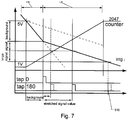
- Fig. 7 shows another embodiment that provides for enhanced resolution. It relies on switching the potential slope of the ramp signal intg between two values: at the beginning, a fast ramp HS is applied as long as no charge has reached in either of the sense nodes. When this happens, i.e., charge is sensed on at least one sense node, the ramp generator RG switches to a ramp function that has a reduced slope, i.e, voltage change as a function of time, thereby increasing the resolution. In the example, the generation of the tap0 pulse switches the ramp generator to generate the ramp with reduced slope. This enables a higher digital resolution on the difference value. For phase measurements, a high resolution of the difference value is much more important than high resolution of the common charge level.
- the time period corresponding to the lower slope region LS is used for the signal difference value (difference of the two outputs from the integration regions).
- the high slope HS is faster than the low slope LS in the example, therefore giving a higher resolution for the difference signal value (LS) than for the background level (HS).
- the low slope (LS) has a steepness of half the nominal slope discussed with reference to Fig. 4 and has a resolution of about 550 electrons per least significant bit (LSB) of counter CTR, and the steep slope has a resolution of 2200 electrons per LSB, in one example.
- the resolution can be increased even more. As you can see, when the signal is too large, the counter comes out-of-range and the information is lost.
- Fig. 8 illustrates another embodiment to overcome this saturation.
- the ramp generator RG switches again to the steeper slope HS2. Then, large signals are converted with a smaller resolution than small signals. The information is compressed but saturation is avoided.
- the switching between the two slopes LS and HS2 has to be fast and accurate (ideally within less than one clock cycle), otherwise non-linearities in the response are introduced.
- the slope over the LS and HS2 periods is logarithmic with increasing slope.
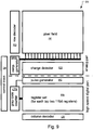
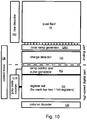
- Figs. 9 and 10 are block diagrams of the digital sensor chip SN with a common ramp generator ( Figs. 5 and 6 ) or with local ramp generators for adapted ramp slope ( Figs. 7 and 8 ).
- the sensor SN includes a pixel field PF.
- a row decoder RD selects one row for read out processing.
- the counter CTR counts up. It is of gray code type to reduce the amount of toggling in the digital part.
- a small control block CB starts and stops both the ramp generator and the counter. These blocks are common for all columns.
- the pulse generator PG ensures that the output of the charge detectors CD is sampled by the counter clock and provides a single pulse to latch the actual counter value.
- the register bank RB is most space consuming item. It has to hold 2 register banks for each tap with the full resolution of the counter (e.g. 11bit). The two register banks are needed for reading the sensor out while the next line is converted.
- the column decoder CD addresses the columns of the pixel field PF.
- Fig. 9 shows the global ramp generator GRG that ramps the integration gates with a specified speed and linearity.
- the ramp signal can be either common for all integration gates or it can be local for each column.
- the speed of the ramp must be adjusted so, that the integration gates are fully discharged within the line time.
- Fig. 10 shows the local ramp generator LRG configuration.
- ramp generators are provided for each pixel so that the two-stage/charge-detection-dependent ramp illustrated in Figs. 7 and 8 is utilized.
- One solution to generate the ramp is to use the existing capacitance of the integration gate, its wiring and additionally an external capacitance (for noise and linearity reasons) and discharge it through a constant current.
- the charge detector CD is a simple SC-circuit containing a one stage inverting amplifier, which implements a high gain. It is reset while a new line is selected and whenever the charge flows out of the integration region and lowers the sense node of the appropriate pixel output by a certain amount, the detector applies a '1' at its output.
- a Schmitt-trigger functionality is applied for a correct setting without ringing.
- the counter must count with high speed from 0 to the maximum resolution. This counter value is then distributed all over the register set, meaning a lot of load is connected to the counter outputs. To reduce the load and therefore also the power consumption and the noise, the counter provides its output Gray coded.
- the counter not only provides the actual code but also the clock for the pulse generator to sample the output of the charge detectors. Because both this clock and the output of the counter are fed from the left side the pulse generator and the register set, the signal arrives at about the same time at both blocks..
- the ramp controller will control the switching between the steep and the plain slope of the ramp on the integration gate. It has to switch to the slow ramp after the first pulse and eventually switch back to the fast one after a given time.
- the pulse generator is attached to the charge detector and generates a pulse whenever the output changes from '0' to '1'. This pulse is then enables the latches in the register set to sample the actual counter value.
- the pulse is going high for a complete clock cycle.
- the register set comprises latches, which will hold the actual counter value when the pulse of the pulse generator arrives.
- the register set actually consists of two sets, one in which the counter value can be stored, the other from which the stored value is taken during read-out. This enables the conversion of a line while the previous line is read-out.
Landscapes
- Physics & Mathematics (AREA)
- Engineering & Computer Science (AREA)
- Computer Networks & Wireless Communication (AREA)
- Electromagnetism (AREA)
- General Physics & Mathematics (AREA)
- Radar, Positioning & Navigation (AREA)
- Remote Sensing (AREA)
- Transforming Light Signals Into Electric Signals (AREA)
- Analogue/Digital Conversion (AREA)
Claims (15)
- Integrierter Sensorchip (CB), der mindestens ein Pixel aufweist, wobei das mindestens eine Pixel aufweist:mindestens zwei Integrationsregionen (IGL; IRL) zum Empfangen und Speichern von photogenerierten Ladungen;eine Modulationsregion (M) zum Bewegen der photogenerierten Ladungen, die in den mindestens zwei Integrationsregionen gespeichert werden sollen;Abtastknoten (SNL; SNR), bei denen jeder der Abtastknoten (SNL; SNR) mit einer der Integrationsregionen (IGL; IGR) assoziiert ist, in die die photogenerierten Ladungen aus den Integrationsregionen (IGL; IGR) während eines Auslesezyklus bewegt werden; und gekennzeichnet dadurch, dass der Chip aufweist:mindestens einen Rampenfunktionsgenerator (RG) zur Erzeugung einer zeitveränderlichen Rampenfunktion (intg), die während des Auslesezyklus auf die Integrationsregionen (IGL; IGR) angewendet wird, um die photogenerierten Ladungen zu den Abtastknoten (SNL; SNR) zu bewegen;einen Zähler (CTR) zum Erzeugen einer Zählung während der Erzeugung der zeitveränderlichen Rampenfunktion (intg);Register (REGL; REGR), wobei jedes der Register (REGL; REGR) während des Auslesezyklus mit einem der Abtastknoten (SNL; SNR) zum Speichern von digitalen Werten assoziiert ist; wobei die Register (REGL; REGR) die Zählung speichern, in Antwort auf den Empfang von photogenerierten Ladungen durch den assoziierten Abtastknoten (SNL; SNR) von den assoziierten Integrationsregionen (IGL; IGR).
- Integrierter Sensorchip nach Anspruch 1, wobei die Modulationsregion (M) Modulationsgates (MGL; MGR) aufweist, die mit jeder der Integrationsregionen (IGL; IGR) assoziiert sind, um ein Driftfeld zu erzeugen, um die photogenerierten Ladungen zwischen den Integrationsregionen (IGL; IGR) zu bewegen.
- Integrierter Sensorchip nach Anspruch 2, wobei die Modulationsregion (M) dazu angepasst ist, photogenerierte Ladungen synchron mit einer Strahlungsquelle zum Beleuchten eines Sichtfeldes des Sensors zu den Integrationsregionen (IGL; IGR) zu bewegen.
- Integrierter Sensorchip nach Anspruch 1, ferner aufweisend Ladungsdetektoren (SAL; SAR), die mit jedem der Abtastknoten (SNL; SNR) assoziiert sind, zur Signalisierung der assoziierten Register (REGL; REGR), wenn die Abtastknoten photogenerierte Ladungen empfangen.
- Integrierter Sensorchip nach Anspruch 1, wobei der Rampenfunktionsgenerator (RG) die zeitveränderliche Rampenfunktion erzeugt, die eine Spannungsrampenfunktion ist.
- Integrierter Sensorchip nach Anspruch 1, wobei der Rampenfunktionsgenerator (RG) die zeitveränderliche Rampenfunktion erzeugen kann, die eine lineare Spannungsrampenfunktion ist.
- Integrierter Sensorchip nach Anspruch 1, wobei der Rampenfunktionsgenerator (RG) die zeitveränderliche Funktion erzeugen kann, die eine logarithmische Spannungsrampenfunktion ist.
- Integrierter Sensorchip nach Anspruch 1, wobei der Rampenfunktionsgenerator (RG) die zeitveränderliche Funktion erzeugen kann, die eine Spannungsrampenfunktion ist, die mindestens zwei Regionen unterschiedlicher Änderungsraten als Funktion der Zeit aufweist.
- Integrierter Sensorchip nach Anspruch 1, wobei der Rampenfunktionsgenerator (RG) die zeitveränderliche Funktion erzeugen kann, die eine Spannungsrampenfunktion ist, die mindestens drei Regionen unterschiedlicher Änderungsraten als Funktion der Zeit aufweist.
- Verfahren zum Auslesen für einen integrierten Sensorchip, aufweisend:Empfangen und Speichern von photogenerierten Ladungen in mindestens zwei Integrationsregionen (IGL; IGR) synchron mit modulierter Strahlung, die eine Szene beleuchtet;Bewegen der photogenerierten Ladungen von einer Modulationsregion (M), um in mindestens zwei Integrationsregionen (IGL; IGR) gespeichert zu werden;gekennzeichnet durch:Bewegen der photogenerierten Ladungen von den Integrationsregionen (IGL; IGR) zu Abtastknoten (SNL; SNR) während eines Auslesezyklus durch Anwenden einer zeitveränderlichen Rampenfunktion (intg) auf die Integrationsregionen (IGL; IGR);Erzeugen einer Zählung während des Erzeugens der zeitveränderlichen Rampenfunktion; undSpeichern der aktuellen Zählung in Antwort auf den Empfang von photogenerierten Ladungen durch den assoziierten Abtastknoten (SNL; SNR) von den assoziierten Integrationsregionen (IGL; IGR).
- Verfahren nach Anspruch 10, wobei die zeitvariable Rampenfunktion (intg) eine Spannungsrampenfunktion ist.
- Verfahren nach Anspruch 10, wobei die zeitvariable Rampenfunktion (intg) eine lineare Spannungsrampenfunktion ist.
- Verfahren nach Anspruch 10, wobei die zeitvariable Rampenfunktion (intg) eine logarithmische Spannungsrampenfunktion ist.
- Verfahren nach Anspruch 10, wobei die zeitvariable Rampenfunktion (intg) eine Spannungsrampenfunktion mit mindestens zwei Regionen unterschiedlicher Änderungsraten als Funktion der Zeit ist.
- Verfahren nach Anspruch 10, wobei die zeitvariable Rampenfunktion (intg) mindestens drei Regionen unterschiedlicher Änderungsraten als Funktion der Zeit aufweist.
Applications Claiming Priority (1)
| Application Number | Priority Date | Filing Date | Title |
|---|---|---|---|
| US95039907P | 2007-07-18 | 2007-07-18 |
Publications (3)
| Publication Number | Publication Date |
|---|---|
| EP2018041A2 EP2018041A2 (de) | 2009-01-21 |
| EP2018041A3 EP2018041A3 (de) | 2012-06-06 |
| EP2018041B1 true EP2018041B1 (de) | 2017-08-23 |
Family
ID=39714111
Family Applications (1)
| Application Number | Title | Priority Date | Filing Date |
|---|---|---|---|
| EP08160757.4A Active EP2018041B1 (de) | 2007-07-18 | 2008-07-18 | Zeitbasierte digitale On-Chip-Konversion von Pixelausgaben |
Country Status (2)
| Country | Link |
|---|---|
| US (1) | US7889257B2 (de) |
| EP (1) | EP2018041B1 (de) |
Families Citing this family (22)
| Publication number | Priority date | Publication date | Assignee | Title |
|---|---|---|---|---|
| JP4107269B2 (ja) * | 2004-02-23 | 2008-06-25 | ソニー株式会社 | 固体撮像装置 |
| US9000349B1 (en) * | 2009-07-31 | 2015-04-07 | Mesa Imaging Ag | Sense node capacitive structure for time of flight sensor |
| KR101884952B1 (ko) * | 2010-01-06 | 2018-08-02 | 헵타곤 마이크로 옵틱스 피티이. 리미티드 | 별도의 화소 및 저장 어레이를 갖는 복조(復調) 센서 |
| US9410800B1 (en) | 2010-08-02 | 2016-08-09 | Heptagon Micro Optics Pte. Ltd. | 3D TOF camera with masked illumination |
| US9857469B2 (en) * | 2010-10-22 | 2018-01-02 | Heptagon Micro Optics Pte. Ltd. | System and method for multi TOF camera operation using phase hopping |
| US9310495B2 (en) * | 2011-05-04 | 2016-04-12 | Oy Ajat Ltd. | Photon/energy identifying X-ray and gamma ray imaging device (“PID”) with a two dimensional array of pixels and system therefrom |
| DE102011081560B4 (de) * | 2011-08-25 | 2024-03-28 | pmdtechnologies ag | Lichtlaufzeitkamerasystem mit Signalpfadüberwachung |
| US9968258B2 (en) * | 2011-09-12 | 2018-05-15 | Tufts University | Imaging fluorescence or luminescence lifetime |
| WO2013041949A1 (en) * | 2011-09-20 | 2013-03-28 | Mesa Imaging Ag | Time of flight sensor with subframe compression and method |
| WO2014000793A1 (en) * | 2012-06-27 | 2014-01-03 | Teledyne Dalsa B.V. | Image sensor and apparatus comprising such image sensor |
| US9746557B2 (en) | 2014-07-25 | 2017-08-29 | Heptagon Micro Optics Pte. Ltd. | Proximity sensor module including time-of-flight sensor wherein a second group of light sensitive elements is in a second one of the chambers of the module |
| US10335036B2 (en) | 2017-11-22 | 2019-07-02 | Hi Llc | Pulsed ultrasound modulated optical tomography using lock-in camera |
| US10016137B1 (en) | 2017-11-22 | 2018-07-10 | Hi Llc | System and method for simultaneously detecting phase modulated optical signals |
| US10219700B1 (en) | 2017-12-15 | 2019-03-05 | Hi Llc | Systems and methods for quasi-ballistic photon optical coherence tomography in diffusive scattering media using a lock-in camera detector |
| US10368752B1 (en) | 2018-03-08 | 2019-08-06 | Hi Llc | Devices and methods to convert conventional imagers into lock-in cameras |
| US11206985B2 (en) | 2018-04-13 | 2021-12-28 | Hi Llc | Non-invasive optical detection systems and methods in highly scattering medium |
| US10812742B2 (en) * | 2018-04-18 | 2020-10-20 | Facebook Technologies, Llc | Apparatus and method for determining whether a photodiode saturates and outputting a digital value representing a charge from that photodiode based on that determination |
| US11857316B2 (en) | 2018-05-07 | 2024-01-02 | Hi Llc | Non-invasive optical detection system and method |
| US11348954B2 (en) * | 2019-03-19 | 2022-05-31 | Samsung Electronics Co., Ltd. | Time-resolving sensor for range measurement and 2D greyscale imaging |
| KR102751168B1 (ko) | 2019-06-19 | 2025-01-13 | 삼성전자주식회사 | 얽힌 픽셀을 포함하는 깊이 센서 |
| US11977162B2 (en) * | 2020-12-26 | 2024-05-07 | Trieye Ltd. | Systems, methods and computer program products for generating depth images based on short-wave infrared detection information |
| KR20230005605A (ko) * | 2021-07-01 | 2023-01-10 | 삼성전자주식회사 | 깊이 센서 및 이를 포함하는 이미지 검출 시스템 |
Citations (2)
| Publication number | Priority date | Publication date | Assignee | Title |
|---|---|---|---|---|
| US6867808B1 (en) * | 1999-03-19 | 2005-03-15 | Scott T. Boden | Time domain imager |
| WO2005120046A2 (en) * | 2004-06-02 | 2005-12-15 | Council For The Central Laboratory Of The Research Councils | Imaging device |
Family Cites Families (27)
| Publication number | Priority date | Publication date | Assignee | Title |
|---|---|---|---|---|
| US5461425A (en) * | 1994-02-15 | 1995-10-24 | Stanford University | CMOS image sensor with pixel level A/D conversion |
| DE4440613C1 (de) | 1994-11-14 | 1996-07-25 | Leica Ag | Vorrichtung und Verfahren zur Detektion und Demodulation eines intensitätsmodulierten Strahlungsfeldes |
| AU715284B2 (en) | 1996-09-05 | 2000-01-20 | Rudolf Schwarte | Method and apparatus for determining the phase and/or amplitude information of an electromagnetic wave |
| US6417882B1 (en) * | 1997-05-06 | 2002-07-09 | Texas Instruments Incorporated | CMOS sensor camera with on-chip image compression |
| US5920274A (en) * | 1997-08-05 | 1999-07-06 | International Business Machines Corporation | Image sensor employing non-uniform A/D conversion |
| US6606122B1 (en) * | 1997-09-29 | 2003-08-12 | California Institute Of Technology | Single chip camera active pixel sensor |
| US6330030B1 (en) * | 1998-01-05 | 2001-12-11 | Intel Corporation | Digital image sensor with low device count per pixel analog-to-digital conversion |
| DE19821974B4 (de) | 1998-05-18 | 2008-04-10 | Schwarte, Rudolf, Prof. Dr.-Ing. | Vorrichtung und Verfahren zur Erfassung von Phase und Amplitude elektromagnetischer Wellen |
| US6522395B1 (en) * | 1999-04-30 | 2003-02-18 | Canesta, Inc. | Noise reduction techniques suitable for three-dimensional information acquirable with CMOS-compatible image sensor ICS |
| US6529240B2 (en) * | 1999-11-18 | 2003-03-04 | Agilent Technologies, Inc. | Random access memory integrated with CMOS sensors |
| US6545624B2 (en) * | 2000-02-11 | 2003-04-08 | Hyundai Electronics Industries Co., Ltd. | Image sensor with analog-to-digital converter that generates a variable slope ramp signal |
| US6515740B2 (en) * | 2000-11-09 | 2003-02-04 | Canesta, Inc. | Methods for CMOS-compatible three-dimensional image sensing using quantum efficiency modulation |
| US6667769B2 (en) * | 2001-12-10 | 2003-12-23 | Motorola, Inc. | Time integrating pixel sensor |
| AU2003223568A1 (en) * | 2002-04-10 | 2003-10-27 | The Johns Hopkins University | The time of flight system on a chip |
| GB2389960A (en) | 2002-06-20 | 2003-12-24 | Suisse Electronique Microtech | Four-tap demodulation pixel |
| US6670904B1 (en) * | 2002-08-22 | 2003-12-30 | Micron Technology, Inc. | Double-ramp ADC for CMOS sensors |
| JP4107269B2 (ja) * | 2004-02-23 | 2008-06-25 | ソニー株式会社 | 固体撮像装置 |
| US7157685B2 (en) * | 2004-04-12 | 2007-01-02 | Canesta, Inc. | Method and system to enhance differential dynamic range and signal/noise in CMOS range finding systems using differential sensors |
| EP1622200A1 (de) | 2004-07-26 | 2006-02-01 | CSEM Centre Suisse d'Electronique et de Microtechnique SA | Festkörper-Fotodetektor-Pixel und Fotodetektionsverfahren |
| EP1635470A1 (de) * | 2004-09-09 | 2006-03-15 | STMicroelectronics Limited | Verfahren und Vorrichtunng zum CMOS-Bildsensor mit einem Kettenverstärker und einem gemultiplexten Analog-Digital-Umwandler |
| KR100744117B1 (ko) * | 2005-08-24 | 2007-08-01 | 삼성전자주식회사 | 손실이 없는 비선형 아날로그 게인 콘트롤러를 지닌 이미지 센서 및 제조 방법 |
| EP1777811B1 (de) * | 2005-10-19 | 2018-10-03 | Heptagon Micro Optics Pte. Ltd. | Verfahren und Vorrichtung zum demodulieren eines modulierten optischen Signals |
| EP1777747B1 (de) | 2005-10-19 | 2008-03-26 | CSEM Centre Suisse d'Electronique et de Microtechnique SA | Einrichtung und Verfahren zur Demodulation von modulierten elektromagnetischen Wellenfeldern |
| US7586077B2 (en) * | 2007-07-18 | 2009-09-08 | Mesa Imaging Ag | Reference pixel array with varying sensitivities for time of flight (TOF) sensor |
| US7804438B2 (en) * | 2008-05-02 | 2010-09-28 | Alexander Krymski | Image sensors and dual ramp analog-to-digital converters and methods |
| KR101543664B1 (ko) * | 2008-12-08 | 2015-08-12 | 삼성전자주식회사 | 픽셀 어레이 및 이를 포함하는 입체 영상 센서 |
| KR101573408B1 (ko) * | 2009-04-29 | 2015-12-02 | 삼성전자주식회사 | 노이즈 제거 수단을 구비한 이미지 센서, 이를 포함하는 이미지 픽업 장치 및 그 방법 |
-
2008
- 2008-07-17 US US12/175,091 patent/US7889257B2/en active Active
- 2008-07-18 EP EP08160757.4A patent/EP2018041B1/de active Active
Patent Citations (2)
| Publication number | Priority date | Publication date | Assignee | Title |
|---|---|---|---|---|
| US6867808B1 (en) * | 1999-03-19 | 2005-03-15 | Scott T. Boden | Time domain imager |
| WO2005120046A2 (en) * | 2004-06-02 | 2005-12-15 | Council For The Central Laboratory Of The Research Councils | Imaging device |
Also Published As
| Publication number | Publication date |
|---|---|
| US20090021617A1 (en) | 2009-01-22 |
| US7889257B2 (en) | 2011-02-15 |
| EP2018041A3 (de) | 2012-06-06 |
| EP2018041A2 (de) | 2009-01-21 |
Similar Documents
| Publication | Publication Date | Title |
|---|---|---|
| EP2018041B1 (de) | Zeitbasierte digitale On-Chip-Konversion von Pixelausgaben | |
| US8223215B2 (en) | Adaptive neighborhood filtering (ANF) system and method for 3D time of flight cameras | |
| EP1493043B1 (de) | Vorrichtung zur erfassung räumlicher information mittels intensitätsmoduliertem licht | |
| EP3474038B1 (de) | Bildsensor zur bestimmung eines dreidimensionalen bildes und verfahren zur bestimmung eines dreidimensionalen bildes | |
| US9625569B2 (en) | Time-of-flight camera with motion detection | |
| Bronzi et al. | 100 000 frames/s 64× 32 single-photon detector array for 2-D imaging and 3-D ranging | |
| EP2017651B2 (de) | Referenzpixelanordnung mit variierenden Sensibilitäten für TOF-Sensor | |
| EP1152261A1 (de) | Vorrichtung und Verfahren zur ortsauflösende Photodetektion und Demodulation von modulierten elektromagnetischen Wellen | |
| CN102693993B (zh) | 电子倍增图像传感器 | |
| US12181610B2 (en) | CMOS image sensor for direct time of flight measurement | |
| CN111103057B (zh) | 具有使用基于电容器的比较器的阈值检测的光子感测 | |
| Sesta et al. | Range-finding SPAD array with smart laser-spot tracking and TDC sharing for background suppression | |
| EP3605148A1 (de) | Festkörperbildgebungsvorrichtung | |
| JP2003247809A (ja) | 距離情報入力装置 | |
| JP2022522952A (ja) | 飛行時間型装置および3d光学検出器 | |
| JP7689346B2 (ja) | 撮像素子および測距装置 | |
| US20250224496A1 (en) | Time-of-flight demodulation circuitry and time-of-flight demodulation method | |
| JPS6024427B2 (ja) | 速度検出装置 | |
| WO2011117162A1 (en) | Optoelectronic sensor and method for detecting impinging-light attribute |
Legal Events
| Date | Code | Title | Description |
|---|---|---|---|
| PUAI | Public reference made under article 153(3) epc to a published international application that has entered the european phase |
Free format text: ORIGINAL CODE: 0009012 |
|
| AK | Designated contracting states |
Kind code of ref document: A2 Designated state(s): AT BE BG CH CY CZ DE DK EE ES FI FR GB GR HR HU IE IS IT LI LT LU LV MC MT NL NO PL PT RO SE SI SK TR |
|
| AX | Request for extension of the european patent |
Extension state: AL BA MK RS |
|
| PUAL | Search report despatched |
Free format text: ORIGINAL CODE: 0009013 |
|
| AK | Designated contracting states |
Kind code of ref document: A3 Designated state(s): AT BE BG CH CY CZ DE DK EE ES FI FR GB GR HR HU IE IS IT LI LT LU LV MC MT NL NO PL PT RO SE SI SK TR |
|
| AX | Request for extension of the european patent |
Extension state: AL BA MK RS |
|
| 17P | Request for examination filed |
Effective date: 20121128 |
|
| AKX | Designation fees paid |
Designated state(s): AT BE BG CH CY CZ LI |
|
| REG | Reference to a national code |
Ref country code: DE Ref legal event code: R108 |
|
| RBV | Designated contracting states (corrected) |
Designated state(s): AT BE BG CH CY CZ DE DK EE ES FI FR GB GR HR HU IE IS IT LI LT LU LV MC MT NL NO PL PT RO SE SI SK TR |
|
| 17Q | First examination report despatched |
Effective date: 20151118 |
|
| RAP1 | Party data changed (applicant data changed or rights of an application transferred) |
Owner name: HEPTAGON MICRO OPTICS PTE. LTD. |
|
| REG | Reference to a national code |
Ref country code: DE Ref legal event code: R079 Ref document number: 602008051727 Country of ref document: DE Free format text: PREVIOUS MAIN CLASS: H04N0003150000 Ipc: G01S0017890000 |
|
| GRAP | Despatch of communication of intention to grant a patent |
Free format text: ORIGINAL CODE: EPIDOSNIGR1 |
|
| STAA | Information on the status of an ep patent application or granted ep patent |
Free format text: STATUS: GRANT OF PATENT IS INTENDED |
|
| RIC1 | Information provided on ipc code assigned before grant |
Ipc: G01S 17/89 20060101AFI20170210BHEP |
|
| INTG | Intention to grant announced |
Effective date: 20170313 |
|
| GRAS | Grant fee paid |
Free format text: ORIGINAL CODE: EPIDOSNIGR3 |
|
| GRAA | (expected) grant |
Free format text: ORIGINAL CODE: 0009210 |
|
| STAA | Information on the status of an ep patent application or granted ep patent |
Free format text: STATUS: THE PATENT HAS BEEN GRANTED |
|
| AK | Designated contracting states |
Kind code of ref document: B1 Designated state(s): AT BE BG CH CY CZ DE DK EE ES FI FR GB GR HR HU IE IS IT LI LT LU LV MC MT NL NO PL PT RO SE SI SK TR |
|
| REG | Reference to a national code |
Ref country code: GB Ref legal event code: FG4D |
|
| REG | Reference to a national code |
Ref country code: CH Ref legal event code: EP |
|
| REG | Reference to a national code |
Ref country code: AT Ref legal event code: REF Ref document number: 921936 Country of ref document: AT Kind code of ref document: T Effective date: 20170915 |
|
| REG | Reference to a national code |
Ref country code: IE Ref legal event code: FG4D |
|
| REG | Reference to a national code |
Ref country code: DE Ref legal event code: R096 Ref document number: 602008051727 Country of ref document: DE |
|
| REG | Reference to a national code |
Ref country code: NL Ref legal event code: FP |
|
| REG | Reference to a national code |
Ref country code: LT Ref legal event code: MG4D |
|
| PG25 | Lapsed in a contracting state [announced via postgrant information from national office to epo] |
Ref country code: HR Free format text: LAPSE BECAUSE OF FAILURE TO SUBMIT A TRANSLATION OF THE DESCRIPTION OR TO PAY THE FEE WITHIN THE PRESCRIBED TIME-LIMIT Effective date: 20170823 Ref country code: NO Free format text: LAPSE BECAUSE OF FAILURE TO SUBMIT A TRANSLATION OF THE DESCRIPTION OR TO PAY THE FEE WITHIN THE PRESCRIBED TIME-LIMIT Effective date: 20171123 Ref country code: SE Free format text: LAPSE BECAUSE OF FAILURE TO SUBMIT A TRANSLATION OF THE DESCRIPTION OR TO PAY THE FEE WITHIN THE PRESCRIBED TIME-LIMIT Effective date: 20170823 Ref country code: LT Free format text: LAPSE BECAUSE OF FAILURE TO SUBMIT A TRANSLATION OF THE DESCRIPTION OR TO PAY THE FEE WITHIN THE PRESCRIBED TIME-LIMIT Effective date: 20170823 |
|
| PG25 | Lapsed in a contracting state [announced via postgrant information from national office to epo] |
Ref country code: LV Free format text: LAPSE BECAUSE OF FAILURE TO SUBMIT A TRANSLATION OF THE DESCRIPTION OR TO PAY THE FEE WITHIN THE PRESCRIBED TIME-LIMIT Effective date: 20170823 Ref country code: ES Free format text: LAPSE BECAUSE OF FAILURE TO SUBMIT A TRANSLATION OF THE DESCRIPTION OR TO PAY THE FEE WITHIN THE PRESCRIBED TIME-LIMIT Effective date: 20170823 Ref country code: BG Free format text: LAPSE BECAUSE OF FAILURE TO SUBMIT A TRANSLATION OF THE DESCRIPTION OR TO PAY THE FEE WITHIN THE PRESCRIBED TIME-LIMIT Effective date: 20171123 Ref country code: GR Free format text: LAPSE BECAUSE OF FAILURE TO SUBMIT A TRANSLATION OF THE DESCRIPTION OR TO PAY THE FEE WITHIN THE PRESCRIBED TIME-LIMIT Effective date: 20171124 Ref country code: IS Free format text: LAPSE BECAUSE OF FAILURE TO SUBMIT A TRANSLATION OF THE DESCRIPTION OR TO PAY THE FEE WITHIN THE PRESCRIBED TIME-LIMIT Effective date: 20171223 Ref country code: PL Free format text: LAPSE BECAUSE OF FAILURE TO SUBMIT A TRANSLATION OF THE DESCRIPTION OR TO PAY THE FEE WITHIN THE PRESCRIBED TIME-LIMIT Effective date: 20170823 |
|
| PG25 | Lapsed in a contracting state [announced via postgrant information from national office to epo] |
Ref country code: DK Free format text: LAPSE BECAUSE OF FAILURE TO SUBMIT A TRANSLATION OF THE DESCRIPTION OR TO PAY THE FEE WITHIN THE PRESCRIBED TIME-LIMIT Effective date: 20170823 Ref country code: CZ Free format text: LAPSE BECAUSE OF FAILURE TO SUBMIT A TRANSLATION OF THE DESCRIPTION OR TO PAY THE FEE WITHIN THE PRESCRIBED TIME-LIMIT Effective date: 20170823 Ref country code: RO Free format text: LAPSE BECAUSE OF FAILURE TO SUBMIT A TRANSLATION OF THE DESCRIPTION OR TO PAY THE FEE WITHIN THE PRESCRIBED TIME-LIMIT Effective date: 20170823 |
|
| REG | Reference to a national code |
Ref country code: DE Ref legal event code: R097 Ref document number: 602008051727 Country of ref document: DE |
|
| PG25 | Lapsed in a contracting state [announced via postgrant information from national office to epo] |
Ref country code: EE Free format text: LAPSE BECAUSE OF FAILURE TO SUBMIT A TRANSLATION OF THE DESCRIPTION OR TO PAY THE FEE WITHIN THE PRESCRIBED TIME-LIMIT Effective date: 20170823 Ref country code: SK Free format text: LAPSE BECAUSE OF FAILURE TO SUBMIT A TRANSLATION OF THE DESCRIPTION OR TO PAY THE FEE WITHIN THE PRESCRIBED TIME-LIMIT Effective date: 20170823 Ref country code: IT Free format text: LAPSE BECAUSE OF FAILURE TO SUBMIT A TRANSLATION OF THE DESCRIPTION OR TO PAY THE FEE WITHIN THE PRESCRIBED TIME-LIMIT Effective date: 20170823 |
|
| REG | Reference to a national code |
Ref country code: FR Ref legal event code: PLFP Year of fee payment: 11 |
|
| PLBE | No opposition filed within time limit |
Free format text: ORIGINAL CODE: 0009261 |
|
| STAA | Information on the status of an ep patent application or granted ep patent |
Free format text: STATUS: NO OPPOSITION FILED WITHIN TIME LIMIT |
|
| 26N | No opposition filed |
Effective date: 20180524 |
|
| REG | Reference to a national code |
Ref country code: DE Ref legal event code: R082 Ref document number: 602008051727 Country of ref document: DE Representative=s name: PROCK, THOMAS, DR., GB Ref country code: DE Ref legal event code: R082 Ref document number: 602008051727 Country of ref document: DE Representative=s name: FISH & RICHARDSON P.C., DE |
|
| PG25 | Lapsed in a contracting state [announced via postgrant information from national office to epo] |
Ref country code: SI Free format text: LAPSE BECAUSE OF FAILURE TO SUBMIT A TRANSLATION OF THE DESCRIPTION OR TO PAY THE FEE WITHIN THE PRESCRIBED TIME-LIMIT Effective date: 20170823 |
|
| PG25 | Lapsed in a contracting state [announced via postgrant information from national office to epo] |
Ref country code: MC Free format text: LAPSE BECAUSE OF FAILURE TO SUBMIT A TRANSLATION OF THE DESCRIPTION OR TO PAY THE FEE WITHIN THE PRESCRIBED TIME-LIMIT Effective date: 20170823 Ref country code: LU Free format text: LAPSE BECAUSE OF NON-PAYMENT OF DUE FEES Effective date: 20180718 |
|
| REG | Reference to a national code |
Ref country code: BE Ref legal event code: MM Effective date: 20180731 |
|
| REG | Reference to a national code |
Ref country code: IE Ref legal event code: MM4A |
|
| PG25 | Lapsed in a contracting state [announced via postgrant information from national office to epo] |
Ref country code: IE Free format text: LAPSE BECAUSE OF NON-PAYMENT OF DUE FEES Effective date: 20180718 |
|
| PG25 | Lapsed in a contracting state [announced via postgrant information from national office to epo] |
Ref country code: BE Free format text: LAPSE BECAUSE OF NON-PAYMENT OF DUE FEES Effective date: 20180731 |
|
| REG | Reference to a national code |
Ref country code: AT Ref legal event code: UEP Ref document number: 921936 Country of ref document: AT Kind code of ref document: T Effective date: 20170823 |
|
| PG25 | Lapsed in a contracting state [announced via postgrant information from national office to epo] |
Ref country code: MT Free format text: LAPSE BECAUSE OF NON-PAYMENT OF DUE FEES Effective date: 20180718 |
|
| PG25 | Lapsed in a contracting state [announced via postgrant information from national office to epo] |
Ref country code: TR Free format text: LAPSE BECAUSE OF FAILURE TO SUBMIT A TRANSLATION OF THE DESCRIPTION OR TO PAY THE FEE WITHIN THE PRESCRIBED TIME-LIMIT Effective date: 20170823 |
|
| REG | Reference to a national code |
Ref country code: DE Ref legal event code: R082 Ref document number: 602008051727 Country of ref document: DE Representative=s name: VIERING, JENTSCHURA & PARTNER MBB PATENT- UND , DE Ref country code: DE Ref legal event code: R082 Ref document number: 602008051727 Country of ref document: DE Representative=s name: PROCK, THOMAS, DR., GB |
|
| PG25 | Lapsed in a contracting state [announced via postgrant information from national office to epo] |
Ref country code: HU Free format text: LAPSE BECAUSE OF FAILURE TO SUBMIT A TRANSLATION OF THE DESCRIPTION OR TO PAY THE FEE WITHIN THE PRESCRIBED TIME-LIMIT; INVALID AB INITIO Effective date: 20080718 Ref country code: PT Free format text: LAPSE BECAUSE OF FAILURE TO SUBMIT A TRANSLATION OF THE DESCRIPTION OR TO PAY THE FEE WITHIN THE PRESCRIBED TIME-LIMIT Effective date: 20170823 |
|
| PG25 | Lapsed in a contracting state [announced via postgrant information from national office to epo] |
Ref country code: CY Free format text: LAPSE BECAUSE OF FAILURE TO SUBMIT A TRANSLATION OF THE DESCRIPTION OR TO PAY THE FEE WITHIN THE PRESCRIBED TIME-LIMIT Effective date: 20170823 |
|
| P01 | Opt-out of the competence of the unified patent court (upc) registered |
Effective date: 20230825 |
|
| REG | Reference to a national code |
Ref country code: DE Ref legal event code: R082 Ref document number: 602008051727 Country of ref document: DE Representative=s name: VIERING, JENTSCHURA & PARTNER MBB PATENT- UND , DE |
|
| REG | Reference to a national code |
Ref country code: DE Ref legal event code: R081 Ref document number: 602008051727 Country of ref document: DE Owner name: AMS-OSRAM ASIA PACIFIC PTE. LTD., SG Free format text: FORMER OWNER: HEPTAGON MICRO OPTICS PTE. LTD., SINGAPORE, SG |
|
| REG | Reference to a national code |
Ref country code: NL Ref legal event code: HC Owner name: AMS-OSRAM ASIA PACIFIC PTE. LTD.; SG Free format text: DETAILS ASSIGNMENT: CHANGE OF OWNER(S), CHANGE OF OWNER(S) NAME; FORMER OWNER NAME: HEPTAGON MICRO OPTICS PTE. LTD. Effective date: 20240830 |
|
| PGFP | Annual fee paid to national office [announced via postgrant information from national office to epo] |
Ref country code: FI Payment date: 20240722 Year of fee payment: 17 |
|
| PGFP | Annual fee paid to national office [announced via postgrant information from national office to epo] |
Ref country code: CH Payment date: 20240801 Year of fee payment: 17 |
|
| PGFP | Annual fee paid to national office [announced via postgrant information from national office to epo] |
Ref country code: AT Payment date: 20240722 Year of fee payment: 17 |
|
| REG | Reference to a national code |
Ref country code: AT Ref legal event code: HC Ref document number: 921936 Country of ref document: AT Kind code of ref document: T Owner name: AMS-OSRAM ASIA PACIFIC PTE. LTD., SG Effective date: 20250424 |
|
| PGFP | Annual fee paid to national office [announced via postgrant information from national office to epo] |
Ref country code: NL Payment date: 20250721 Year of fee payment: 18 |
|
| PGFP | Annual fee paid to national office [announced via postgrant information from national office to epo] |
Ref country code: DE Payment date: 20250722 Year of fee payment: 18 |
|
| PGFP | Annual fee paid to national office [announced via postgrant information from national office to epo] |
Ref country code: GB Payment date: 20250722 Year of fee payment: 18 |
|
| PGFP | Annual fee paid to national office [announced via postgrant information from national office to epo] |
Ref country code: FR Payment date: 20250724 Year of fee payment: 18 |