EP2017651B2 - Referenzpixelanordnung mit variierenden Sensibilitäten für TOF-Sensor - Google Patents
Referenzpixelanordnung mit variierenden Sensibilitäten für TOF-Sensor Download PDFInfo
- Publication number
- EP2017651B2 EP2017651B2 EP08160698.0A EP08160698A EP2017651B2 EP 2017651 B2 EP2017651 B2 EP 2017651B2 EP 08160698 A EP08160698 A EP 08160698A EP 2017651 B2 EP2017651 B2 EP 2017651B2
- Authority
- EP
- European Patent Office
- Prior art keywords
- pixels
- light
- pixel array
- reference pixel
- rpa
- Prior art date
- Legal status (The legal status is an assumption and is not a legal conclusion. Google has not performed a legal analysis and makes no representation as to the accuracy of the status listed.)
- Active
Links
Images


Classifications
-
- G—PHYSICS
- G01—MEASURING; TESTING
- G01S—RADIO DIRECTION-FINDING; RADIO NAVIGATION; DETERMINING DISTANCE OR VELOCITY BY USE OF RADIO WAVES; LOCATING OR PRESENCE-DETECTING BY USE OF THE REFLECTION OR RERADIATION OF RADIO WAVES; ANALOGOUS ARRANGEMENTS USING OTHER WAVES
- G01S7/00—Details of systems according to groups G01S13/00, G01S15/00, G01S17/00
- G01S7/48—Details of systems according to groups G01S13/00, G01S15/00, G01S17/00 of systems according to group G01S17/00
- G01S7/481—Constructional features, e.g. arrangements of optical elements
- G01S7/4816—Constructional features, e.g. arrangements of optical elements of receivers alone
-
- G—PHYSICS
- G01—MEASURING; TESTING
- G01S—RADIO DIRECTION-FINDING; RADIO NAVIGATION; DETERMINING DISTANCE OR VELOCITY BY USE OF RADIO WAVES; LOCATING OR PRESENCE-DETECTING BY USE OF THE REFLECTION OR RERADIATION OF RADIO WAVES; ANALOGOUS ARRANGEMENTS USING OTHER WAVES
- G01S17/00—Systems using the reflection or reradiation of electromagnetic waves other than radio waves, e.g. lidar systems
- G01S17/02—Systems using the reflection of electromagnetic waves other than radio waves
- G01S17/06—Systems determining position data of a target
- G01S17/42—Simultaneous measurement of distance and other co-ordinates
-
- G—PHYSICS
- G01—MEASURING; TESTING
- G01S—RADIO DIRECTION-FINDING; RADIO NAVIGATION; DETERMINING DISTANCE OR VELOCITY BY USE OF RADIO WAVES; LOCATING OR PRESENCE-DETECTING BY USE OF THE REFLECTION OR RERADIATION OF RADIO WAVES; ANALOGOUS ARRANGEMENTS USING OTHER WAVES
- G01S17/00—Systems using the reflection or reradiation of electromagnetic waves other than radio waves, e.g. lidar systems
- G01S17/88—Lidar systems specially adapted for specific applications
- G01S17/89—Lidar systems specially adapted for specific applications for mapping or imaging
- G01S17/894—Three-dimensional [3D] imaging with simultaneous measurement of time-of-flight at a two-dimensional [2D] array of receiver pixels, e.g. time-of-flight cameras or flash lidar
-
- G—PHYSICS
- G01—MEASURING; TESTING
- G01S—RADIO DIRECTION-FINDING; RADIO NAVIGATION; DETERMINING DISTANCE OR VELOCITY BY USE OF RADIO WAVES; LOCATING OR PRESENCE-DETECTING BY USE OF THE REFLECTION OR RERADIATION OF RADIO WAVES; ANALOGOUS ARRANGEMENTS USING OTHER WAVES
- G01S7/00—Details of systems according to groups G01S13/00, G01S15/00, G01S17/00
- G01S7/48—Details of systems according to groups G01S13/00, G01S15/00, G01S17/00 of systems according to group G01S17/00
- G01S7/497—Means for monitoring or calibrating
Definitions
- Time of flight (TOF) sensors typically utilize charge-coupled device (CCD) or complementary metal oxide semiconductor (CMOS) based technologies that are able to sample at high speed.
- CCD charge-coupled device
- CMOS complementary metal oxide semiconductor
- the typical application is for point distance sensing or three-dimensional (3D) imaging in which the scene of interest is actively illuminated with modulated illuminating radiation and the sensor sampling is performed synchronously with the illuminating radiation.
- High speed sensors are also useful in other applications such as fluorescence lifetime imaging.
- Drift fields are created in this region to transfer the charge carriers to one or more integration gates where the charge is stored until a readout stage.
- specific integration gates are assigned to different phases within the period of the stimulation radiation and the drift fields are modulated synchronously with the simulation radiation in order to move the charge carriers from the photosensitive region to the integration gates for the phase assigned to that gate.
- German patent application DE19821974A1 (Schwarte, Vorplatz und Maschinen GmbH und Maschinen GmbH für Ü Kunststofftechnik für Ü Kunststoff Kunststoff Kunststoff Wellen, 1999), see also US Pat. No. 6,825,455 B1 , disclosed a photon-mixing element for a TOF sensor.
- a photon-mixing element for a TOF sensor In order to get a pixel with high-sensitivity and high-speed demodulation facility, a combined structure of stripe-like elements, each of them with short transport paths, is proposed. Nevertheless, the stripe-like structure leads to a poor fill-factor because the regions between the stripes are not photosensitive.
- WO 2007/045108 A1 presents a newer TOF sensor example.
- the drift field over most or all of the photosensitive area is basically static in time.
- the static or quasi static field in the photosensitive region moves or the dumps the charge carriers into a typically smaller modulated region, which may or may not be photosensitive.
- the charge carriers are then swept from the modulated region into integration regions or gates synchronously with the modulated signal.
- This newer system can operate at much higher frequencies because modulation is over a much smaller area, having a lower intrinsic capacitance, whereas transport within the large photosensitive region can be optimized for speed.
- the newer demodulation device avoids trade-offs between the sensitivity/fill-factor and the demodulation speed. Both aspects can be optimized in the pixel at the same time.
- US 6,483,094B1 presents another technology to measure the time of flight.
- the invention consists of a solid state optical shutter device to demodulate the received light and therefore, in combination with a conventional imager, is able to resolve the TOF information.
- the optical shutter is placed in front of the imager. It consists of a photodiode as input and a light emitting diode as output. The gate in the photodiode and the light emitting diode can be controlled to enable / disable the electron transfer from the photodiode to the LED. This allows a high-speed demodulation of the received modulated light, hence gathering TOF information.
- US-2006/228050 discloses a method for calibrating 3D image sensors.
- the aim of this method is to calibrate the entire receiving array with respect to every pixel.
- the entire receiving array is illuminated at defined intervals exclusively with one modulated light source.
- the emitted light source can be used via a deflection device.
- Two different distances can be simulated by carrying out two calibrating measurements with different phase relations between emitted and received signal, thereby making it possible to detect distance-related errors for every pixel individually.
- the method described does not make use of a chip having an image pixel array and a separate reference picture array.
- single point distance measurement devices In the past, in single point distance measurement devices, this problem of synchronization and calibration has usually been solved by using references inside the device or by feeding back part of the light from the modulated light source to a second receiver.
- single point distance measurement devices in general only consist of one single light element illumination unit. Hence, only part of the light from this single light element has to be fed back to the receiver as calibration measurement.
- the illumination unit usually includes an array of several, even hundreds of, light elements, such as light emitting diodes or laser diode elements.
- light elements such as light emitting diodes or laser diode elements.
- simply feeding back part of the light from one element of the modulated light source is usually inadequate since the other light elements might behave differently.
- the light elements might have different temperature behaviors, manufacturing tolerances in speed, different life time changes, for example.
- the back-reflected light derived from one single light element does not necessarily represent the overall emitted light wavefront generated by the array of light elements of the modulated light source.
- the back-reflected light is fed on a reference receiver separate from the main image sensor, it also suffers from different behaviors, e.g. over temperature, lifetime, manufacturing tolerances, than the main receiver itself. It is desirable to have the reference receiver on the same chip and have exactly the same control circuitry as the pixels on the image sensor themselves.
- the exposure time is adjusted to optimize the signal to noise (S/N) level on the image sensor.
- the reference pixels have the same exposure time as the pixels that are used for image sensing. However, in that case, by changing the exposure time, the energy captured by the reference pixels varies, which in some cases can push the reference pixels into saturation for high exposure times or the S/N ratio on the reference pixels is too low for evaluation in the case of for very short exposure times.
- the invention features a demodulation sensor in accordance with claim 1.
- phase delays between an optical signal and an electronic reference signal are three-dimensional (3D) range measurement, fluorescence imaging, or optical communication.
- the acquisition of the distance information is accomplished by the measurement of the time-of-flight (TOF). That is the time the light needs for the round-trip from the measurement camera or sensor system to the object and back again to the system.
- TOF time-of-flight
- Fig. 1 illustrates the basic principle of such a 3D-measurement system.
- Modulated light ML1 from a light source or illumination module IM of a camera or sensor 100 is sent to the object OB of a scene.
- a fraction of the total optical power sent out returns as reflected modulated light ML2 to the camera 100 and detected by the image sensor SN.
- the sensor SN comprises a single pixel (point ranging) or a pixel matrix IPA comprised of a one or two dimensional array of demodulation imaging pixels IP.
- Each imaging pixel IP is capable of demodulating the impinging light signal, which also includes any background light BG.
- a controller C regulates the timing of the camera 100.
- the phase values of each imaging pixel IP correspond to the particular distance information of one point in the scene.
- the entire imaging pixel array IPA is read out and displayed for example on a monitor/personal computer M.
- Either pulse intensity-modulated, continuously intensity-modulated light (e.g. sine wave or other modulation codes like pseudo-random sequences) is sent out by the illumination module or light source IM, reflected by the object OB and detected by the sensor SN. If each imaging pixel IP of the sensor SN is capable of demodulating the optical signal at the same time, the sensor SN is able to deliver 3D images in real-time, i.e., frame rates of up to 30 Hertz (Hz), or even more, are possible. In pulse operation the demodulation would deliver the time of flight directly.
- Hz Hertz
- Figs. 2A and 2B show the relationship between signals for the case of continuous sinusoidal modulation and the signal sampling. Although this specific modulation scheme is highlighted in the following, the utilization of the synchronization is not restricted to this particular scheme. Any other modulation scheme is applicable: e.g. pulse, rectangular, pseudo-noise or chirp modulation. Only the final extraction of the distance information is different.
- Fig. 2A shows both the modulated emitted signal ML1 and signal RS received by the sensor SN.
- Signal RS includes the reflected portion of the emitted signal ML2 and background light BG.
- the amplitude A corresponds to MS2, and offset B corresponds to the background in the received signal RS.
- the phase offset P between both signals, ML1, RS, is unknown, but it can be unambiguously reconstructed by sampling the received signal RS.
- phase offset error D between the illumination drive signal IDS produced by the controller C and the modulated emitted signal ML1. This error corresponds to any other delays associated with generation of the emitted signal ML1 and timing and/or sampling of the imaging sensor SN.
- a sampling with four samples per modulation period is depicted.
- Each sample is an integration of the electrical signal over a duration dt that is a predefined fraction of the modulation period.
- the photo-generated charges are accumulated over several modulation periods, in some embodiments.
- a reference pixel array RPA is further provided, according to the principles of the present invention.
- This reference pixel array RPA receives light directly from the illumination module IM.
- a light guide LG is provided for transmitting reference modulation light MLR to the reference pixel array RPA.
- the sensitivity of the reference pixel array RPA to the reference modulated light MLR is varied for different reference pixels RP of the reference pixel array RPA as illustrated by shading V.
- the different sensitivities of the reference pixels RP in the RPA are achieved by designing the pixels to have different light sensitivities with respect to each other.
- the different sensitivities are achieved by changing the optical coupling between the separate reference pixels RP of the reference pixel array RPA to the reference modulated light MLR such as by changing how the different reference pixels RP couple to the aperture LGA of the light guide LG.
- Fig. 3 illustrates the relationship between the imaging pixel array IPA, the reference pixel array RPA and controller C.
- the controller C reads out the image information and time of flight information from the imaging pixel array IPA. In order to analyze the time of flight information, the controller receives a sync signal generated by a reference pixel evaluator SEL.
- the reference pixel array RPA comprises a series of reference pixels RP1-RPn.
- the reference pixel array RPA comprises pixels RP1-RPn that have varying degrees of light sensitive LS and light insensitive LIS regions. Specifically, in the illustrated example, the proportion of the light sensitive LS to light insensitive LIS regions for the pixels RP1-RPn increases across the lateral extent of the reference pixel array RPA.
- the reference pixel evaluator SEL generates the sync signal to the controller C based on information from selected pixels within the reference pixel array RPA. This sync signal provides a "zero distance" value, which is used to calibrate the phase measurements of all image pixels.
- the reference pixel evaluator SEL selects one pixel or weights and averages multiple pixels of the reference pixel array RPA based on whether the pixels are receiving an adequate signal but are not in saturation. As indicated in Fig. 3 , it is desired that the control signals supplied by the controller C are exactly the same for the image pixel array IPA and for the reference pixel array RPA. In this way, the reference pixel array RPA is controlled with the same exposure time as the imaging pixel array IPA. Nevertheless, due to different sensitivities in the reference pixel array RPA, pixels are always available for use by the evaluator SEL due to the different sensitivities provided in the RPA.
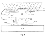
- Fig. 4 illustrates the arrangement of the camera 100.
- the imaging module IM comprises an illumination board 412.
- This illumination board 412 in turn comprises a series of light elements 414.
- theses light elements 414 are light emitting diodes and/or laser diodes.
- a protection shield 420 separates the illumination module IM from the external environment. This protection shield 420 is often transparent only to the light of the wavelength generated by the light emitting elements 414. Most of the modulated light generated by the illumination module IM and passing through the protection shield 420 is the modulated light transmitted to the scene or object of interest (ML1).
- ML1 object of interest
- a portion of the light is transmitted by internal reflection, for example, as reference modulated light MLR to the light guide LG that is attached to a lateral side of the protection shield 420, in the illustrated implementation.
- the light guide LG carries the reference light MLR to the reference pixel array RPA on the sensor chip SN.
- the reference pixel array RPA is located laterally to and on the same chip with the image pixel array IPA.
- a light shield 421 projects vertically from the sensor SN to prevent light from the light guide LG from reaching the pixels of the imaging pixel array IPA.
- the imaging pixel array IPA is sensitive largely or only to the light returning from the scene ML2+BG.
- the light returning from the field in the illustrated example is received through the protection shield 420.
- a lens array 410 is located in a central port 418 in the illumination board 412. This central lens system 410 focuses the returning light ML2+BG onto the imaging pixel array IPA.
- Figs 5A and 5B are schematic diagrams illustrating the relationship between the reference pixel array RPA and the imaging pixel array IPA according to two implementations.
- Fig. 5A shows a first implementation of the reference pixel array RPA and its relationship to the imaging pixel array IPA.
- the reference pixel array RPA is a line having only a single pixel width or multiple pixel width. It extends over an entire length of the imaging pixel array IPA. In this way, every line and/or every row of the imaging pixel array has a corresponding pixel in the reference pixel array RPA on the sensor chip SN.
- the reference pixel array is controlled by exactly the same signals as the imaging pixel array (IPA).
- Fig. 5B shows a second implementation of the sensor chip SN.
- the reference pixel array RPA comprises a square or rectangular field that is adjacent to and smaller than the imaging pixel array IPA. It does not extend over the entire row or column of the imaging pixel field array IPA. Preferably it comprises a series of pixels in a two-dimensional array.
- Fig. 6 shows how the sensitive area LS and non-sensitive area LIS changes across the extent of the reference pixel array RPA.
- the light pixel RP1 at one extreme end of the reference pixel array RPA has a large light sensitive region LS in relationship to the light insensitive region LIS of the reference pixel.
- Reference pixel RP5, near to the center of the reference pixel array RPA has a much larger light insensitive region LIS relative to light sensitive region LS; whereas at the other extreme of the reference pixel array RPA, the light insensitive region LIS is very large in respect to the light sensitive region LS.
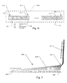
- Fig. 7 illustrates another embodiment.
- all of the pixels of the reference pixel array RPA can have the same inherent sensitivity to the light in one example, although this is not required. Specifically, they all would typically have the same proportion of light insensitive to light sensitive regions across the extent of the reference pixel array RPA.
- sensitivity of the reference pixel array RPA to the reference modulated light MLR is varied for different reference pixels RP of the reference pixel array RPA by changing how light guide LG is coupled to across the length of the reference pixel array RPA.
- reference pixel RP1 that is closer to the light guide aperture LGA, receives more light than reference pixels RPn that are farther from this aperture.
- the reference pixels will be available that will not be in saturation even as the level of the reference modulated light MLR changes or the integration periods or exposure times change.
Landscapes
- Engineering & Computer Science (AREA)
- Physics & Mathematics (AREA)
- Computer Networks & Wireless Communication (AREA)
- General Physics & Mathematics (AREA)
- Radar, Positioning & Navigation (AREA)
- Remote Sensing (AREA)
- Electromagnetism (AREA)
- Optical Radar Systems And Details Thereof (AREA)
- Facsimile Heads (AREA)
Claims (6)
- Demodulationssensor mit:einem Beleuchtungsmodul (IM) für erzeugtes moduliertes Licht für die Beleuchtung eines Schauplatzes;einem oder mehreren Abbildungspixeln für das Erfassen des modulierten Lichts, das von dem Schauplatz zurückkommt;einer Anordnung von Referenzpixeln in einer Referenzpixelanordnung (RPA) für den Empfang von moduliertem Referenzlicht (MLR) aus dem Beleuchtungsmodul (IM), wobei die Referenzpixel (RP, RPn) in der Referenzpixelanordnung (RPA) unterschiedliche Empfindlichkeiten für das modulierte Referenzlicht aus dem Beleuchtungsmodul aufweisen,wobei sich die unterschiedlichen Empfindlichkeiten entweder aus der unterschiedlichen Ankopplung an einen Lichtleiter (LG), durch den das Referenzlicht (MLR) aus dem Beleuchtungsmodul (IM) auf die Referenzpixelanordnung (RPA) übertragen wird, den unterschiedlichen optischen Empfindlichkeiten oder den unterschiedlichen Anteilen von lichtempfindlichen (LS) und nicht lichtunempfindlichen (LIS) Bereichen in den Pixeln ergeben; undeinem Steuerglied (C) zum Bestimmen einer Phasenbeziehung zwischen dem modulierten Licht, das durch das Beleuchtungsmodul (IM) bezüglich der Referenzpixelanordnung (RPA) erzeugt wird, und dem modulierten Licht, das durch das eine oder die mehreren Abbildungspixel erfasst wird,wobei die Anordnung von Referenzpixeln (RPA) eine ein- oder zweidimensionale Anordnung von Referenzpixeln auf einem gleichen Chip wie das eine oder die mehreren Abbildungspixel und benachbart zu den Abbildungspixeln umfasst und ferner einen Lichtschutz (421) umfassend, der von dem Chip zwischen den Referenzpixeln und dem einen oder den mehreren Abbildungspixeln herausragt, um zu verhindern, dass das Referenzlicht das eine oder die mehreren Abbildungspixel erreicht.
- Sensor nach Anspruch 1, wobei das eine oder die mehreren Abbildungspixel ein einziges Pixel für die Punktentfernungsbestimmung umfassen.
- Sensor nach Anspruch 1, wobei das eine oder die mehreren Abbildungspixel eine ein- oder zweidimensionale Anordnung von Abbildungspixeln für das Erzeugen eines Bildes des Schauplatzes umfassen.
- Sensor nach Anspruch 1, ferner eine Referenzpixel- Auswerteeinheit (SEL)zum Erzeugen eines Synchronisierungssignals an das Steuerglied in Reaktion auf die ausgewählten Pixel in der Referenzpixelanordnung (RPA) umfassend.
- Sensor nach Anspruch 1, ferner eine Referenzpixel- Auswerteeinheit (SEL) zum Erzeugen eines Synchronisierungssignals an das Steuerglied (C) in Reaktion auf die Pixel umfassend, die aus der Referenzpixelanordnung (RPA) basierend darauf ausgewählt sind, 1) welche der Pixel gesättigt sind oder nicht und 2) welche der Pixel ein gutes SRV aufweisen oder nicht.
- Sensor nach Anspruch 1, Auswerteeinheit (SEL) ferner eine Referenzpixel zum Erzeugen eines Synchronisierungssignals an das Steuerglied in Reaktion auf die Pixel umfassend, die aus der Referenzpixelanordnung (RPA) basierend auf einer Mittelung und/oder Wichtung einer Phasenbeziehung ausgewählt sind, die auf einem oder mehreren der Referenzpixel in der Referenzpixelanordnung (RPA) beruht.
Applications Claiming Priority (1)
| Application Number | Priority Date | Filing Date | Title |
|---|---|---|---|
| US95041207P | 2007-07-18 | 2007-07-18 |
Publications (4)
| Publication Number | Publication Date |
|---|---|
| EP2017651A2 EP2017651A2 (de) | 2009-01-21 |
| EP2017651A3 EP2017651A3 (de) | 2011-03-09 |
| EP2017651B1 EP2017651B1 (de) | 2012-06-06 |
| EP2017651B2 true EP2017651B2 (de) | 2015-09-30 |
Family
ID=39876740
Family Applications (1)
| Application Number | Title | Priority Date | Filing Date |
|---|---|---|---|
| EP08160698.0A Active EP2017651B2 (de) | 2007-07-18 | 2008-07-18 | Referenzpixelanordnung mit variierenden Sensibilitäten für TOF-Sensor |
Country Status (2)
| Country | Link |
|---|---|
| US (1) | US7586077B2 (de) |
| EP (1) | EP2017651B2 (de) |
Cited By (2)
| Publication number | Priority date | Publication date | Assignee | Title |
|---|---|---|---|---|
| DE102017101501B3 (de) * | 2017-01-26 | 2018-01-04 | Sick Ag | Optoelektronischer Sensor und Verfahren zur Bestimmung der Entfernung eines Objekts in einem Überwachungsbereich |
| DE102014111431B4 (de) | 2014-08-11 | 2024-07-11 | Infineon Technologies Ag | Flugzeitvorrichtungen |
Families Citing this family (52)
| Publication number | Priority date | Publication date | Assignee | Title |
|---|---|---|---|---|
| US7889257B2 (en) * | 2007-07-18 | 2011-02-15 | Mesa Imaging Ag | On-chip time-based digital conversion of pixel outputs |
| US9000353B2 (en) | 2010-06-22 | 2015-04-07 | President And Fellows Of Harvard College | Light absorption and filtering properties of vertically oriented semiconductor nano wires |
| US8748799B2 (en) | 2010-12-14 | 2014-06-10 | Zena Technologies, Inc. | Full color single pixel including doublet or quadruplet si nanowires for image sensors |
| US9299866B2 (en) | 2010-12-30 | 2016-03-29 | Zena Technologies, Inc. | Nanowire array based solar energy harvesting device |
| US8299472B2 (en) | 2009-12-08 | 2012-10-30 | Young-June Yu | Active pixel sensor with nanowire structured photodetectors |
| US8229255B2 (en) | 2008-09-04 | 2012-07-24 | Zena Technologies, Inc. | Optical waveguides in image sensors |
| US8735797B2 (en) | 2009-12-08 | 2014-05-27 | Zena Technologies, Inc. | Nanowire photo-detector grown on a back-side illuminated image sensor |
| US9478685B2 (en) | 2014-06-23 | 2016-10-25 | Zena Technologies, Inc. | Vertical pillar structured infrared detector and fabrication method for the same |
| US9343490B2 (en) | 2013-08-09 | 2016-05-17 | Zena Technologies, Inc. | Nanowire structured color filter arrays and fabrication method of the same |
| US8274039B2 (en) | 2008-11-13 | 2012-09-25 | Zena Technologies, Inc. | Vertical waveguides with various functionality on integrated circuits |
| US9515218B2 (en) | 2008-09-04 | 2016-12-06 | Zena Technologies, Inc. | Vertical pillar structured photovoltaic devices with mirrors and optical claddings |
| US9406709B2 (en) | 2010-06-22 | 2016-08-02 | President And Fellows Of Harvard College | Methods for fabricating and using nanowires |
| US8866065B2 (en) | 2010-12-13 | 2014-10-21 | Zena Technologies, Inc. | Nanowire arrays comprising fluorescent nanowires |
| US8003928B1 (en) * | 2008-12-16 | 2011-08-23 | Hrl Laboratories, Llc | Method for compensating a millimeter wave imaging array |
| US9000349B1 (en) * | 2009-07-31 | 2015-04-07 | Mesa Imaging Ag | Sense node capacitive structure for time of flight sensor |
| US8416125B1 (en) | 2009-11-03 | 2013-04-09 | Hrl Laboratories, Llc | Radiative noise adding compensation for MMW sensor arrays |
| US20110298579A1 (en) * | 2010-06-08 | 2011-12-08 | Cedes Safety & Automation Ag | Dynamically adaptable safety zones |
| US9410800B1 (en) * | 2010-08-02 | 2016-08-09 | Heptagon Micro Optics Pte. Ltd. | 3D TOF camera with masked illumination |
| DE102010043768B3 (de) * | 2010-09-30 | 2011-12-15 | Ifm Electronic Gmbh | Lichtlaufzeitkamera |
| KR101722641B1 (ko) | 2010-12-23 | 2017-04-04 | 삼성전자주식회사 | 3차원 영상 획득 장치 및 상기 3차원 영상 획득 장치에서 깊이 정보를 추출하는 방법 |
| KR101887099B1 (ko) * | 2010-12-29 | 2018-08-09 | 삼성전자주식회사 | 이미지 처리 시스템 및 이미지 처리 방법 |
| DE102011005740A1 (de) | 2011-03-17 | 2012-09-20 | Robert Bosch Gmbh | Messvorrichtung zur Messung einer Entfernung zwischen der Messvorrichtung und einem Zielobjekt mit Hilfe optischer Messstrahlung |
| US9182491B2 (en) | 2011-05-06 | 2015-11-10 | Waikatolink Limited | Selective distance range imaging |
| DE102011081560B4 (de) * | 2011-08-25 | 2024-03-28 | pmdtechnologies ag | Lichtlaufzeitkamerasystem mit Signalpfadüberwachung |
| DE102012019471B4 (de) * | 2012-09-28 | 2023-12-21 | Carl Zeiss Microscopy Gmbh | Vorrichtung und Verfahren zum Ermitteln von Stoffeigenschaften |
| JP6127558B2 (ja) * | 2013-02-13 | 2017-05-17 | オムロン株式会社 | 撮像装置 |
| US10401498B2 (en) | 2013-06-06 | 2019-09-03 | Ams Sensors Singapore Pte. Ltd. | Sensor system with active illumination |
| DE102013109020B4 (de) * | 2013-08-21 | 2016-06-09 | Pmdtechnologies Gmbh | Streulichtreferenzpixel |
| SG11201606511YA (en) * | 2014-03-14 | 2016-09-29 | Heptagon Micro Optics Pte Ltd | Optical imaging modules and optical detection modules including a time-of-flight sensor |
| SG11201606510XA (en) | 2014-03-14 | 2016-09-29 | Heptagon Micro Optics Pte Ltd | Optoelectronic modules operable to recognize spurious reflections and to compensate for errors caused by spurious reflections |
| DE102015207567B4 (de) * | 2014-05-02 | 2026-01-08 | pmdtechnologies ag | Lichtformungsoptik und Lichtleiterstruktur für einen Lichtlaufzeitsensor |
| US9420149B2 (en) * | 2014-06-13 | 2016-08-16 | Lips Corporation | Integrated depth camera |
| US10054675B2 (en) * | 2014-10-24 | 2018-08-21 | Analog Devices, Inc. | Active compensation for phase alignment errors in time-of-flight cameras |
| WO2016076796A1 (en) * | 2014-11-12 | 2016-05-19 | Heptagon Micro Optics Pte. Ltd. | Optoelectronic modules for distance measurements and/or multi-dimensional imaging |
| DE102015204125B4 (de) * | 2015-03-06 | 2018-04-05 | pmdtechnologies ag | Auskoppelelement für einen Lichtleiter zur Lichtführung an einem Lichtlaufzeitsensor |
| US9638791B2 (en) * | 2015-06-25 | 2017-05-02 | Qualcomm Incorporated | Methods and apparatus for performing exposure estimation using a time-of-flight sensor |
| US11067691B2 (en) | 2015-11-13 | 2021-07-20 | Ams Sensors Singapore Pte. Ltd. | Acquisition of distance data with optical ranging systems |
| US10829280B2 (en) * | 2015-12-03 | 2020-11-10 | Drop Water Corporation | Compostable single-use beverage container and associated mechanism for sealing the container |
| TWI731026B (zh) | 2016-01-15 | 2021-06-21 | 新加坡商海特根微光學公司 | 半導體器件 |
| DE102016219172B3 (de) * | 2016-10-04 | 2018-01-25 | Ifm Electronic Gmbh | Referenzpixelanordnung für einen Bildsensor |
| DE102016015759A1 (de) | 2016-10-04 | 2018-04-05 | Ifm Electronic Gmbh | Referenzpixelanordnung für einen Bildsensor |
| US10420469B2 (en) | 2017-11-22 | 2019-09-24 | Hi Llc | Optical detection system for determining neural activity in brain based on water concentration |
| US10016137B1 (en) | 2017-11-22 | 2018-07-10 | Hi Llc | System and method for simultaneously detecting phase modulated optical signals |
| US10219700B1 (en) | 2017-12-15 | 2019-03-05 | Hi Llc | Systems and methods for quasi-ballistic photon optical coherence tomography in diffusive scattering media using a lock-in camera detector |
| US10368752B1 (en) | 2018-03-08 | 2019-08-06 | Hi Llc | Devices and methods to convert conventional imagers into lock-in cameras |
| CN111886856B (zh) * | 2018-03-26 | 2024-10-15 | 索尼公司 | 成像元件、成像装置以及信息处理方法 |
| US11206985B2 (en) | 2018-04-13 | 2021-12-28 | Hi Llc | Non-invasive optical detection systems and methods in highly scattering medium |
| US11857316B2 (en) | 2018-05-07 | 2024-01-02 | Hi Llc | Non-invasive optical detection system and method |
| JP2020060433A (ja) | 2018-10-10 | 2020-04-16 | ソニーセミコンダクタソリューションズ株式会社 | 測距システム、キャリブレーション方法、プログラム、及び電子機器 |
| CN112789514B (zh) * | 2018-10-31 | 2024-07-09 | 索尼半导体解决方案公司 | 电子设备、方法及计算机程序 |
| JP2020085477A (ja) * | 2018-11-16 | 2020-06-04 | ソニーセミコンダクタソリューションズ株式会社 | 光測距装置及び光測距方法 |
| WO2023011091A1 (en) * | 2021-08-03 | 2023-02-09 | Congying Sui | An imaging method and system based on wise-pixels with valved modulation |
Citations (1)
| Publication number | Priority date | Publication date | Assignee | Title |
|---|---|---|---|---|
| WO1998010255A1 (de) † | 1996-09-05 | 1998-03-12 | Rudolf Schwarte | Verfahren und vorrichtung zur bestimmung der phasen- und/oder amplitudeninformation einer elektromagnetischen welle |
Family Cites Families (7)
| Publication number | Priority date | Publication date | Assignee | Title |
|---|---|---|---|---|
| DE4440613C1 (de) | 1994-11-14 | 1996-07-25 | Leica Ag | Vorrichtung und Verfahren zur Detektion und Demodulation eines intensitätsmodulierten Strahlungsfeldes |
| JP2002508885A (ja) * | 1997-04-08 | 2002-03-19 | スリーディーヴィー システムズ リミテッド | 固体光シャッタ |
| DE19821974B4 (de) * | 1998-05-18 | 2008-04-10 | Schwarte, Rudolf, Prof. Dr.-Ing. | Vorrichtung und Verfahren zur Erfassung von Phase und Amplitude elektromagnetischer Wellen |
| GB2389960A (en) | 2002-06-20 | 2003-12-24 | Suisse Electronique Microtech | Four-tap demodulation pixel |
| DE10259135A1 (de) * | 2002-12-18 | 2004-07-01 | Conti Temic Microelectronic Gmbh | Verfahren und Anordnung zur Referenzierung von 3D Bildaufnehmern |
| US7274467B2 (en) * | 2005-01-04 | 2007-09-25 | Carl Zeiss Smt Ag | Phase shifting interferometric method, interferometer apparatus and method of manufacturing an optical element |
| ATE390715T1 (de) | 2005-10-19 | 2008-04-15 | Suisse Electronique Microtech | Einrichtung und verfahren zur demodulation von modulierten elektromagnetischen wellenfeldern |
-
2008
- 2008-07-17 US US12/175,100 patent/US7586077B2/en active Active
- 2008-07-18 EP EP08160698.0A patent/EP2017651B2/de active Active
Patent Citations (1)
| Publication number | Priority date | Publication date | Assignee | Title |
|---|---|---|---|---|
| WO1998010255A1 (de) † | 1996-09-05 | 1998-03-12 | Rudolf Schwarte | Verfahren und vorrichtung zur bestimmung der phasen- und/oder amplitudeninformation einer elektromagnetischen welle |
Non-Patent Citations (1)
| Title |
|---|
| X. LUAN: "Experimental Investigation of Photonic Mixer Device and Development of TOF 3D Ranging Systems Based on PMD Technology", DISSERTATION, November 2001 (2001-11-01) † |
Cited By (2)
| Publication number | Priority date | Publication date | Assignee | Title |
|---|---|---|---|---|
| DE102014111431B4 (de) | 2014-08-11 | 2024-07-11 | Infineon Technologies Ag | Flugzeitvorrichtungen |
| DE102017101501B3 (de) * | 2017-01-26 | 2018-01-04 | Sick Ag | Optoelektronischer Sensor und Verfahren zur Bestimmung der Entfernung eines Objekts in einem Überwachungsbereich |
Also Published As
| Publication number | Publication date |
|---|---|
| EP2017651B1 (de) | 2012-06-06 |
| EP2017651A2 (de) | 2009-01-21 |
| EP2017651A3 (de) | 2011-03-09 |
| US7586077B2 (en) | 2009-09-08 |
| US20090020687A1 (en) | 2009-01-22 |
Similar Documents
| Publication | Publication Date | Title |
|---|---|---|
| EP2017651B2 (de) | Referenzpixelanordnung mit variierenden Sensibilitäten für TOF-Sensor | |
| US7834985B2 (en) | Surface profile measurement | |
| US8223215B2 (en) | Adaptive neighborhood filtering (ANF) system and method for 3D time of flight cameras | |
| JP4405154B2 (ja) | イメージングシステムおよび物体の画像を取得する方法 | |
| US9325920B2 (en) | Processing of time-of-flight signals | |
| US11703567B2 (en) | Measuring device having scanning functionality and settable receiving ranges of the receiver | |
| EP2594959B1 (de) | System und Verfahren für Mehrfach-TOF-Kamerabetrieb mit Phasensprung | |
| CN111108407B (zh) | 半导体主体和用于飞行时间测量的方法 | |
| US20180081041A1 (en) | LiDAR with irregular pulse sequence | |
| US9316735B2 (en) | Proximity detection apparatus and associated methods having single photon avalanche diodes for determining a quality metric based upon the number of events | |
| EP3182156B1 (de) | Sortiervorrichtung | |
| Kahlmann et al. | Calibration for increased accuracy of the range imaging camera swissranger | |
| US11592292B2 (en) | Total station or theodolite having scanning functionality and settable receiving ranges of the receiver | |
| US10908266B2 (en) | Time of flight distance sensor | |
| US8355117B2 (en) | Method and arrangement for measuring the distance to an object | |
| CN101449181B (zh) | 测距方法和用于确定目标的空间维度的测距仪 | |
| CN109791205A (zh) | 用于从成像阵列中的像素单元的曝光值减除背景光的方法以及用于该方法的像素单元 | |
| WO2020190920A1 (en) | Dynamic range improvements in lidar applications | |
| US20220171038A1 (en) | Multichannel time-of-flight measurement device with time-to-digital converters in a programmable integrated circuit | |
| US7391505B2 (en) | Range sensing system | |
| Bronzi et al. | 3D Sensor for indirect ranging with pulsed laser source | |
| Kotake et al. | Performance improvement of real-time 3D imaging ladar based on a modified array receiver | |
| RU186487U1 (ru) | Устройство для круглосуточного наблюдения положения пятна излучения на удалённом объекте | |
| GB2485991A (en) | Camera using a Single Photon Avalanche Diode (SPAD) array |
Legal Events
| Date | Code | Title | Description |
|---|---|---|---|
| PUAI | Public reference made under article 153(3) epc to a published international application that has entered the european phase |
Free format text: ORIGINAL CODE: 0009012 |
|
| AK | Designated contracting states |
Kind code of ref document: A2 Designated state(s): AT BE BG CH CY CZ DE DK EE ES FI FR GB GR HR HU IE IS IT LI LT LU LV MC MT NL NO PL PT RO SE SI SK TR |
|
| AX | Request for extension of the european patent |
Extension state: AL BA MK RS |
|
| PUAL | Search report despatched |
Free format text: ORIGINAL CODE: 0009013 |
|
| AK | Designated contracting states |
Kind code of ref document: A3 Designated state(s): AT BE BG CH CY CZ DE DK EE ES FI FR GB GR HR HU IE IS IT LI LT LU LV MC MT NL NO PL PT RO SE SI SK TR |
|
| AX | Request for extension of the european patent |
Extension state: AL BA MK RS |
|
| 17P | Request for examination filed |
Effective date: 20110414 |
|
| AKX | Designation fees paid |
Designated state(s): AT BE BG CH CY CZ DE DK EE ES FI FR GB GR HR HU IE IS IT LI LT LU LV MC MT NL NO PL PT RO SE SI SK TR |
|
| GRAP | Despatch of communication of intention to grant a patent |
Free format text: ORIGINAL CODE: EPIDOSNIGR1 |
|
| GRAS | Grant fee paid |
Free format text: ORIGINAL CODE: EPIDOSNIGR3 |
|
| GRAA | (expected) grant |
Free format text: ORIGINAL CODE: 0009210 |
|
| AK | Designated contracting states |
Kind code of ref document: B1 Designated state(s): AT BE BG CH CY CZ DE DK EE ES FI FR GB GR HR HU IE IS IT LI LT LU LV MC MT NL NO PL PT RO SE SI SK TR |
|
| REG | Reference to a national code |
Ref country code: GB Ref legal event code: FG4D |
|
| REG | Reference to a national code |
Ref country code: AT Ref legal event code: REF Ref document number: 561272 Country of ref document: AT Kind code of ref document: T Effective date: 20120615 Ref country code: CH Ref legal event code: EP |
|
| REG | Reference to a national code |
Ref country code: IE Ref legal event code: FG4D |
|
| REG | Reference to a national code |
Ref country code: DE Ref legal event code: R096 Ref document number: 602008016138 Country of ref document: DE Effective date: 20120802 |
|
| REG | Reference to a national code |
Ref country code: SE Ref legal event code: TRGR |
|
| REG | Reference to a national code |
Ref country code: NL Ref legal event code: T3 |
|
| PG25 | Lapsed in a contracting state [announced via postgrant information from national office to epo] |
Ref country code: CY Free format text: LAPSE BECAUSE OF FAILURE TO SUBMIT A TRANSLATION OF THE DESCRIPTION OR TO PAY THE FEE WITHIN THE PRESCRIBED TIME-LIMIT Effective date: 20120606 Ref country code: LT Free format text: LAPSE BECAUSE OF FAILURE TO SUBMIT A TRANSLATION OF THE DESCRIPTION OR TO PAY THE FEE WITHIN THE PRESCRIBED TIME-LIMIT Effective date: 20120606 Ref country code: NO Free format text: LAPSE BECAUSE OF FAILURE TO SUBMIT A TRANSLATION OF THE DESCRIPTION OR TO PAY THE FEE WITHIN THE PRESCRIBED TIME-LIMIT Effective date: 20120906 Ref country code: FI Free format text: LAPSE BECAUSE OF FAILURE TO SUBMIT A TRANSLATION OF THE DESCRIPTION OR TO PAY THE FEE WITHIN THE PRESCRIBED TIME-LIMIT Effective date: 20120606 |
|
| REG | Reference to a national code |
Ref country code: AT Ref legal event code: MK05 Ref document number: 561272 Country of ref document: AT Kind code of ref document: T Effective date: 20120606 |
|
| REG | Reference to a national code |
Ref country code: LT Ref legal event code: MG4D Effective date: 20120606 |
|
| PG25 | Lapsed in a contracting state [announced via postgrant information from national office to epo] |
Ref country code: HR Free format text: LAPSE BECAUSE OF FAILURE TO SUBMIT A TRANSLATION OF THE DESCRIPTION OR TO PAY THE FEE WITHIN THE PRESCRIBED TIME-LIMIT Effective date: 20120606 Ref country code: GR Free format text: LAPSE BECAUSE OF FAILURE TO SUBMIT A TRANSLATION OF THE DESCRIPTION OR TO PAY THE FEE WITHIN THE PRESCRIBED TIME-LIMIT Effective date: 20120907 Ref country code: LV Free format text: LAPSE BECAUSE OF FAILURE TO SUBMIT A TRANSLATION OF THE DESCRIPTION OR TO PAY THE FEE WITHIN THE PRESCRIBED TIME-LIMIT Effective date: 20120606 Ref country code: SI Free format text: LAPSE BECAUSE OF FAILURE TO SUBMIT A TRANSLATION OF THE DESCRIPTION OR TO PAY THE FEE WITHIN THE PRESCRIBED TIME-LIMIT Effective date: 20120606 |
|
| PG25 | Lapsed in a contracting state [announced via postgrant information from national office to epo] |
Ref country code: BE Free format text: LAPSE BECAUSE OF FAILURE TO SUBMIT A TRANSLATION OF THE DESCRIPTION OR TO PAY THE FEE WITHIN THE PRESCRIBED TIME-LIMIT Effective date: 20120606 Ref country code: SK Free format text: LAPSE BECAUSE OF FAILURE TO SUBMIT A TRANSLATION OF THE DESCRIPTION OR TO PAY THE FEE WITHIN THE PRESCRIBED TIME-LIMIT Effective date: 20120606 Ref country code: EE Free format text: LAPSE BECAUSE OF FAILURE TO SUBMIT A TRANSLATION OF THE DESCRIPTION OR TO PAY THE FEE WITHIN THE PRESCRIBED TIME-LIMIT Effective date: 20120606 Ref country code: RO Free format text: LAPSE BECAUSE OF FAILURE TO SUBMIT A TRANSLATION OF THE DESCRIPTION OR TO PAY THE FEE WITHIN THE PRESCRIBED TIME-LIMIT Effective date: 20120606 Ref country code: CZ Free format text: LAPSE BECAUSE OF FAILURE TO SUBMIT A TRANSLATION OF THE DESCRIPTION OR TO PAY THE FEE WITHIN THE PRESCRIBED TIME-LIMIT Effective date: 20120606 Ref country code: IS Free format text: LAPSE BECAUSE OF FAILURE TO SUBMIT A TRANSLATION OF THE DESCRIPTION OR TO PAY THE FEE WITHIN THE PRESCRIBED TIME-LIMIT Effective date: 20121006 Ref country code: AT Free format text: LAPSE BECAUSE OF FAILURE TO SUBMIT A TRANSLATION OF THE DESCRIPTION OR TO PAY THE FEE WITHIN THE PRESCRIBED TIME-LIMIT Effective date: 20120606 |
|
| PG25 | Lapsed in a contracting state [announced via postgrant information from national office to epo] |
Ref country code: PL Free format text: LAPSE BECAUSE OF FAILURE TO SUBMIT A TRANSLATION OF THE DESCRIPTION OR TO PAY THE FEE WITHIN THE PRESCRIBED TIME-LIMIT Effective date: 20120606 Ref country code: MC Free format text: LAPSE BECAUSE OF NON-PAYMENT OF DUE FEES Effective date: 20120731 Ref country code: IT Free format text: LAPSE BECAUSE OF FAILURE TO SUBMIT A TRANSLATION OF THE DESCRIPTION OR TO PAY THE FEE WITHIN THE PRESCRIBED TIME-LIMIT Effective date: 20120606 Ref country code: PT Free format text: LAPSE BECAUSE OF FAILURE TO SUBMIT A TRANSLATION OF THE DESCRIPTION OR TO PAY THE FEE WITHIN THE PRESCRIBED TIME-LIMIT Effective date: 20121008 |
|
| PLBI | Opposition filed |
Free format text: ORIGINAL CODE: 0009260 |
|
| 26 | Opposition filed |
Opponent name: IFM ELECTRONIC GMBH/PMDTECHNOLOGIES GMBH Effective date: 20130228 |
|
| PLAX | Notice of opposition and request to file observation + time limit sent |
Free format text: ORIGINAL CODE: EPIDOSNOBS2 |
|
| PG25 | Lapsed in a contracting state [announced via postgrant information from national office to epo] |
Ref country code: ES Free format text: LAPSE BECAUSE OF FAILURE TO SUBMIT A TRANSLATION OF THE DESCRIPTION OR TO PAY THE FEE WITHIN THE PRESCRIBED TIME-LIMIT Effective date: 20120917 Ref country code: DK Free format text: LAPSE BECAUSE OF FAILURE TO SUBMIT A TRANSLATION OF THE DESCRIPTION OR TO PAY THE FEE WITHIN THE PRESCRIBED TIME-LIMIT Effective date: 20120606 |
|
| REG | Reference to a national code |
Ref country code: IE Ref legal event code: MM4A |
|
| REG | Reference to a national code |
Ref country code: DE Ref legal event code: R026 Ref document number: 602008016138 Country of ref document: DE Effective date: 20130228 |
|
| PLAF | Information modified related to communication of a notice of opposition and request to file observations + time limit |
Free format text: ORIGINAL CODE: EPIDOSCOBS2 |
|
| PG25 | Lapsed in a contracting state [announced via postgrant information from national office to epo] |
Ref country code: BG Free format text: LAPSE BECAUSE OF FAILURE TO SUBMIT A TRANSLATION OF THE DESCRIPTION OR TO PAY THE FEE WITHIN THE PRESCRIBED TIME-LIMIT Effective date: 20120906 Ref country code: MT Free format text: LAPSE BECAUSE OF FAILURE TO SUBMIT A TRANSLATION OF THE DESCRIPTION OR TO PAY THE FEE WITHIN THE PRESCRIBED TIME-LIMIT Effective date: 20120606 Ref country code: IE Free format text: LAPSE BECAUSE OF NON-PAYMENT OF DUE FEES Effective date: 20120718 |
|
| PLBB | Reply of patent proprietor to notice(s) of opposition received |
Free format text: ORIGINAL CODE: EPIDOSNOBS3 |
|
| PG25 | Lapsed in a contracting state [announced via postgrant information from national office to epo] |
Ref country code: TR Free format text: LAPSE BECAUSE OF FAILURE TO SUBMIT A TRANSLATION OF THE DESCRIPTION OR TO PAY THE FEE WITHIN THE PRESCRIBED TIME-LIMIT Effective date: 20120606 |
|
| PG25 | Lapsed in a contracting state [announced via postgrant information from national office to epo] |
Ref country code: LU Free format text: LAPSE BECAUSE OF NON-PAYMENT OF DUE FEES Effective date: 20120718 |
|
| PG25 | Lapsed in a contracting state [announced via postgrant information from national office to epo] |
Ref country code: HU Free format text: LAPSE BECAUSE OF FAILURE TO SUBMIT A TRANSLATION OF THE DESCRIPTION OR TO PAY THE FEE WITHIN THE PRESCRIBED TIME-LIMIT Effective date: 20080718 |
|
| REG | Reference to a national code |
Ref country code: CH Ref legal event code: PL |
|
| REG | Reference to a national code |
Ref country code: DE Ref legal event code: R082 Ref document number: 602008016138 Country of ref document: DE Representative=s name: PETERREINS SCHLEY PATENT- UND RECHTSANWAELTE, DE Ref country code: DE Ref legal event code: R082 Ref document number: 602008016138 Country of ref document: DE Representative=s name: FISH & RICHARDSON P.C., DE |
|
| REG | Reference to a national code |
Ref country code: CH Ref legal event code: AECN Free format text: DAS PATENT IST AUFGRUND DES WEITERBEHANDLUNGSANTRAGS VOM 10. MAERZ 2015 REAKTIVIERT WORDEN. |
|
| REG | Reference to a national code |
Ref country code: FR Ref legal event code: PLFP Year of fee payment: 8 |
|
| REG | Reference to a national code |
Ref country code: DE Ref legal event code: R082 Ref document number: 602008016138 Country of ref document: DE Representative=s name: FISH & RICHARDSON P.C., DE Ref country code: DE Ref legal event code: R082 Ref document number: 602008016138 Country of ref document: DE Representative=s name: PETERREINS SCHLEY PATENT- UND RECHTSANWAELTE, DE |
|
| PUAH | Patent maintained in amended form |
Free format text: ORIGINAL CODE: 0009272 |
|
| STAA | Information on the status of an ep patent application or granted ep patent |
Free format text: STATUS: PATENT MAINTAINED AS AMENDED |
|
| 27A | Patent maintained in amended form |
Effective date: 20150930 |
|
| AK | Designated contracting states |
Kind code of ref document: B2 Designated state(s): AT BE BG CH CY CZ DE DK EE ES FI FR GB GR HR HU IE IS IT LI LT LU LV MC MT NL NO PL PT RO SE SI SK TR |
|
| REG | Reference to a national code |
Ref country code: DE Ref legal event code: R102 Ref document number: 602008016138 Country of ref document: DE Ref country code: CH Ref legal event code: AELC |
|
| REG | Reference to a national code |
Ref country code: SE Ref legal event code: RPEO |
|
| REG | Reference to a national code |
Ref country code: DE Ref legal event code: R082 Ref document number: 602008016138 Country of ref document: DE Representative=s name: PROCK, THOMAS, DR., GB Ref country code: DE Ref legal event code: R082 Ref document number: 602008016138 Country of ref document: DE Representative=s name: FISH & RICHARDSON P.C., DE Ref country code: DE Ref legal event code: R082 Ref document number: 602008016138 Country of ref document: DE Representative=s name: PETERREINS SCHLEY PATENT- UND RECHTSANWAELTE, DE Ref country code: DE Ref legal event code: R081 Ref document number: 602008016138 Country of ref document: DE Owner name: HEPTAGON MICRO OPTICS PTE. LTD., SG Free format text: FORMER OWNER: MESA IMAGING AG, ZUERICH, CH |
|
| REG | Reference to a national code |
Ref country code: NL Ref legal event code: FP |
|
| REG | Reference to a national code |
Ref country code: GB Ref legal event code: 732E Free format text: REGISTERED BETWEEN 20160211 AND 20160217 |
|
| REG | Reference to a national code |
Ref country code: CH Ref legal event code: PUE Owner name: HEPTAGON MICRO OPTICS PTE. LTD., SG Free format text: FORMER OWNER: MESA IMAGING AG, CH |
|
| REG | Reference to a national code |
Ref country code: FR Ref legal event code: TP Owner name: HEPTAGON MICRO OPTICS PTE. LTD., SG Effective date: 20160502 Ref country code: FR Ref legal event code: CA Effective date: 20160502 |
|
| REG | Reference to a national code |
Ref country code: FR Ref legal event code: PLFP Year of fee payment: 9 |
|
| REG | Reference to a national code |
Ref country code: CH Ref legal event code: NV Representative=s name: SCHNEIDER FELDMANN AG PATENT- UND MARKENANWAEL, CH |
|
| REG | Reference to a national code |
Ref country code: NL Ref legal event code: PD Owner name: HEPTAGON MICRO OPTICS PTE. LTD.; SG Free format text: DETAILS ASSIGNMENT: VERANDERING VAN EIGENAAR(S), OVERDRACHT; FORMER OWNER NAME: MESA IMAGING AG Effective date: 20160921 |
|
| REG | Reference to a national code |
Ref country code: FR Ref legal event code: PLFP Year of fee payment: 10 |
|
| REG | Reference to a national code |
Ref country code: FR Ref legal event code: PLFP Year of fee payment: 11 |
|
| REG | Reference to a national code |
Ref country code: DE Ref legal event code: R082 Ref document number: 602008016138 Country of ref document: DE Representative=s name: PROCK, THOMAS, DR., GB Ref country code: DE Ref legal event code: R082 Ref document number: 602008016138 Country of ref document: DE Representative=s name: FISH & RICHARDSON P.C., DE |
|
| REG | Reference to a national code |
Ref country code: DE Ref legal event code: R082 Ref document number: 602008016138 Country of ref document: DE Representative=s name: VIERING, JENTSCHURA & PARTNER MBB PATENT- UND , DE Ref country code: DE Ref legal event code: R082 Ref document number: 602008016138 Country of ref document: DE Representative=s name: PROCK, THOMAS, DR., GB |
|
| REG | Reference to a national code |
Ref country code: CH Ref legal event code: PFA Owner name: HEPTAGON MICRO OPTICS PTE. LTD., SG Free format text: FORMER OWNER: HEPTAGON MICRO OPTICS PTE. LTD., SG |
|
| P01 | Opt-out of the competence of the unified patent court (upc) registered |
Effective date: 20230825 |
|
| REG | Reference to a national code |
Ref country code: DE Ref legal event code: R082 Ref document number: 602008016138 Country of ref document: DE Representative=s name: VIERING, JENTSCHURA & PARTNER MBB PATENT- UND , DE |
|
| REG | Reference to a national code |
Ref country code: DE Ref legal event code: R081 Ref document number: 602008016138 Country of ref document: DE Owner name: AMS-OSRAM ASIA PACIFIC PTE. LTD., SG Free format text: FORMER OWNER: HEPTAGON MICRO OPTICS PTE. LTD., SINGAPORE, SG |
|
| REG | Reference to a national code |
Ref country code: NL Ref legal event code: HC Owner name: AMS-OSRAM ASIA PACIFIC PTE. LTD.; SG Free format text: DETAILS ASSIGNMENT: CHANGE OF OWNER(S), CHANGE OF OWNER(S) NAME; FORMER OWNER NAME: HEPTAGON MICRO OPTICS PTE. LTD. Effective date: 20240830 |
|
| PGFP | Annual fee paid to national office [announced via postgrant information from national office to epo] |
Ref country code: CH Payment date: 20240801 Year of fee payment: 17 |
|
| PGFP | Annual fee paid to national office [announced via postgrant information from national office to epo] |
Ref country code: SE Payment date: 20240719 Year of fee payment: 17 |
|
| PGFP | Annual fee paid to national office [announced via postgrant information from national office to epo] |
Ref country code: NL Payment date: 20250721 Year of fee payment: 18 |
|
| PGFP | Annual fee paid to national office [announced via postgrant information from national office to epo] |
Ref country code: DE Payment date: 20250722 Year of fee payment: 18 |
|
| PGFP | Annual fee paid to national office [announced via postgrant information from national office to epo] |
Ref country code: GB Payment date: 20250722 Year of fee payment: 18 |
|
| PGFP | Annual fee paid to national office [announced via postgrant information from national office to epo] |
Ref country code: FR Payment date: 20250724 Year of fee payment: 18 |
|
| REG | Reference to a national code |
Ref country code: CH Ref legal event code: H13 Free format text: ST27 STATUS EVENT CODE: U-0-0-H10-H13 (AS PROVIDED BY THE NATIONAL OFFICE) Effective date: 20260224 |