EP2016593B1 - Manipulationsdetektion und -schutz für gehäuse - Google Patents
Manipulationsdetektion und -schutz für gehäuse Download PDFInfo
- Publication number
- EP2016593B1 EP2016593B1 EP07755879.9A EP07755879A EP2016593B1 EP 2016593 B1 EP2016593 B1 EP 2016593B1 EP 07755879 A EP07755879 A EP 07755879A EP 2016593 B1 EP2016593 B1 EP 2016593B1
- Authority
- EP
- European Patent Office
- Prior art keywords
- magnetic field
- memory storage
- storage cell
- enclosure
- state
- Prior art date
- Legal status (The legal status is an assumption and is not a legal conclusion. Google has not performed a legal analysis and makes no representation as to the accuracy of the status listed.)
- Active
Links
- 238000001514 detection method Methods 0.000 title description 13
- 230000005291 magnetic effect Effects 0.000 claims description 103
- 210000000352 storage cell Anatomy 0.000 claims description 63
- 230000005055 memory storage Effects 0.000 claims description 54
- 239000000463 material Substances 0.000 claims description 8
- 238000000926 separation method Methods 0.000 claims description 6
- 230000007423 decrease Effects 0.000 claims description 2
- 239000004020 conductor Substances 0.000 claims 4
- 239000011343 solid material Substances 0.000 claims 1
- 210000004027 cell Anatomy 0.000 description 84
- 230000015654 memory Effects 0.000 description 19
- 230000005415 magnetization Effects 0.000 description 12
- 230000008878 coupling Effects 0.000 description 7
- 238000010168 coupling process Methods 0.000 description 7
- 238000005859 coupling reaction Methods 0.000 description 7
- 230000005641 tunneling Effects 0.000 description 7
- 230000008859 change Effects 0.000 description 5
- 239000000696 magnetic material Substances 0.000 description 5
- 239000003302 ferromagnetic material Substances 0.000 description 4
- 239000000758 substrate Substances 0.000 description 4
- RYGMFSIKBFXOCR-UHFFFAOYSA-N Copper Chemical compound [Cu] RYGMFSIKBFXOCR-UHFFFAOYSA-N 0.000 description 3
- 229910052802 copper Inorganic materials 0.000 description 3
- 239000010949 copper Substances 0.000 description 3
- 238000013500 data storage Methods 0.000 description 3
- 238000010586 diagram Methods 0.000 description 3
- 230000000694 effects Effects 0.000 description 3
- 230000008901 benefit Effects 0.000 description 2
- 230000005540 biological transmission Effects 0.000 description 2
- 230000001419 dependent effect Effects 0.000 description 2
- 238000005259 measurement Methods 0.000 description 2
- 230000007246 mechanism Effects 0.000 description 2
- 238000004382 potting Methods 0.000 description 2
- 230000004044 response Effects 0.000 description 2
- 230000005290 antiferromagnetic effect Effects 0.000 description 1
- 230000006399 behavior Effects 0.000 description 1
- 230000015572 biosynthetic process Effects 0.000 description 1
- 150000001875 compounds Chemical class 0.000 description 1
- 238000009792 diffusion process Methods 0.000 description 1
- 238000005530 etching Methods 0.000 description 1
- 230000002349 favourable effect Effects 0.000 description 1
- 230000005294 ferromagnetic effect Effects 0.000 description 1
- 230000005381 magnetic domain Effects 0.000 description 1
- 238000001465 metallisation Methods 0.000 description 1
- 230000006911 nucleation Effects 0.000 description 1
- 238000010899 nucleation Methods 0.000 description 1
- TWNQGVIAIRXVLR-UHFFFAOYSA-N oxo(oxoalumanyloxy)alumane Chemical compound O=[Al]O[Al]=O TWNQGVIAIRXVLR-UHFFFAOYSA-N 0.000 description 1
- 230000035699 permeability Effects 0.000 description 1
- 238000007789 sealing Methods 0.000 description 1
- 230000003746 surface roughness Effects 0.000 description 1
- 210000000635 valve cell Anatomy 0.000 description 1
Images


Classifications
-
- G—PHYSICS
- G01—MEASURING; TESTING
- G01R—MEASURING ELECTRIC VARIABLES; MEASURING MAGNETIC VARIABLES
- G01R33/00—Arrangements or instruments for measuring magnetic variables
- G01R33/02—Measuring direction or magnitude of magnetic fields or magnetic flux
- G01R33/06—Measuring direction or magnitude of magnetic fields or magnetic flux using galvano-magnetic devices
- G01R33/09—Magnetoresistive devices
- G01R33/093—Magnetoresistive devices using multilayer structures, e.g. giant magnetoresistance sensors
-
- B—PERFORMING OPERATIONS; TRANSPORTING
- B82—NANOTECHNOLOGY
- B82Y—SPECIFIC USES OR APPLICATIONS OF NANOSTRUCTURES; MEASUREMENT OR ANALYSIS OF NANOSTRUCTURES; MANUFACTURE OR TREATMENT OF NANOSTRUCTURES
- B82Y25/00—Nanomagnetism, e.g. magnetoimpedance, anisotropic magnetoresistance, giant magnetoresistance or tunneling magnetoresistance
-
- G—PHYSICS
- G11—INFORMATION STORAGE
- G11C—STATIC STORES
- G11C11/00—Digital stores characterised by the use of particular electric or magnetic storage elements; Storage elements therefor
- G11C11/02—Digital stores characterised by the use of particular electric or magnetic storage elements; Storage elements therefor using magnetic elements
- G11C11/16—Digital stores characterised by the use of particular electric or magnetic storage elements; Storage elements therefor using magnetic elements using elements in which the storage effect is based on magnetic spin effect
- G11C11/165—Auxiliary circuits
- G11C11/1695—Protection circuits or methods
Definitions
- the present invention relates to enclosures desired to be secure against having the contents thereof revealed as a result of tampering therewith that results in intrusion therein or to the removal of some or all of the those contents therefrom, or both, and, more particularly, to magnetic devices for providing such security.
- enclosures are used to store various kinds of items that an owner or user wants secure against being revealed to, or removed by, others especially without the owner or user gaining knowledge of such revelations or removals having occurred.
- One example is an enclosure for keeping selected data stored in a computer or other device memory secret. To do so, such data must be protected against its being extracted from the memory, or from being intercepted from transmissions thereof during use, in a manner which would result in the contents thereof being revealed.
- the data is encrypted before storage in the memory or before transmission to better protect the contents thereof from being revealed.
- Such arrangements require the use of encryption and decryption keys as the basis for encrypting the data and for decrypting the coded data result which are often kept in nonvolatile memories in the form of integrated circuits stored in an enclosure. These enclosures are subject to many kinds of attacks by those interested in gaining unauthorized access to the contents of the data stored therein. Thus, there is a desire to provide an arrangement for detecting any intrusions into such enclosures with little additional apparatus and, in at least some situations, to erase such stored data from the nonvolatile memory upon an intrusion.
- EP 1588371 against which the preamble is begled on
- WO 2004/055822 disclose tamper protection arrangements in which tampering is detected by noting when a magnetic enclosure is removed from the vicinity of a magnetic field sensing device.
- the present invention provides a tamper detecting enclosure arrangement for an enclosure containing an interior space in which a protected item is positioned, the arrangement comprising a magnetoresistive sensing memory storage cell positioned in or near the protected item in the enclosure having a magnetoresistance versus externally applied magnetic field characteristic with first and second states of differing resistive values.
- the memory storage cell enters the second state from the first state in the presence of a magnetic field magnitude that is less than a first threshold magnetic field value, and the memory storage cell is initially written to be in the first state when it is positioned in or near the protected item in the enclosure.
- a magnet is positioned at a selected initial separation distance from the magnetoresistive sensing memory storage cell to thereby provide a magnetic field of initial magnitude to the magnetoresistive sensing memory storage cell that is between the first threshold magnetic field value and a second threshold magnetic field value, which magnetic field decreases below the first threshold magnetic field value if said enclosure is opened so as to result in substantially increasing a distance separating the magnet and the magnetoresistive sensing memory storage cell, as a resulting opening separation distance, that is larger than the initial separation distance.
- the arrangement is characterised in that the memory storage cell enters the first state from the second state in the presence of a magnetic field magnitude that is greater than the second threshold magnetic field value, the second threshold magnetic field value being larger than the first threshold magnetic field value.
- An antitampering device is provided as primarily a magnetic memory having one or more data storage cells that are sensitive to exteriorly applied magnetic fields in such a way as to guarantee a measurable change in magnetic states of the cells as a result of any sufficient intrusion to provide access to that which is being protected by those cells.
- the arrangements described below all use magnetoresistance changes in one or more sensing memory storage cells in the antitampering device. Detection of the intrusion is accomplished even though the antitampering device is not provided with any operating electrical power which is a decided advantage in many situations.
- These antitampering devices can be provided so as to assure that information that was originally stored is completely erased and so be undetectable after the tampering sensed by the antitampering device.
- the antitampering devices described below responds when the absolute magnetic field about them becomes relatively small but does not react when such magnetic fields are maintained relatively large, such responses being obtained from sensing memory storage cells in the device having an asymmetrical electrical resistance versus applied magnetic field characteristic.
- This kind of antitampering device can provide only detection of tampering with the pertinent enclosure, or it can provide such tampering detection and thereafter disable the protected system so that so that proprietary information also kept in the enclosure is not revealed.
- An integrated circuit chip for example, having a tampering detection magnetoresistive sensing memory storage cell or cells therein, and also containing common operating memory cells in which is stored data to be protected, can be positioned in a protected enclosure, 10, having a receptacle, 11, and a cover, 12, as shown (all just partially shown) in the cross section side view in the representative schematic diagram of Figure 1A , or the chip can be contained in an integrated circuit chip housing of nonmagnetic material positioned in enclosure 10.
- a permanent magnet, 13, is positioned in enclosure cover 12.
- Such a cover is provided to deny unwanted access by others to the interior of receptacle 11 in enclosure 10, and so to such an integrated circuit chip, 14, on a printed circuit board, 15, positioned therein, without such intruders leaving an indication of that intrusive access, but still allowing nondestructive access to this interior by a rightful possessor if needed (also with an indication of such an access intrusion).
- At least one tampering detection magnetoresistive sensing memory storage cell, 16, is provided in integrated circuit 14.
- the outer sides of the enclosure can have some permeable magnetic material therein or thereon to shield the interior of the enclosure from external magnetic fields but small enough permeability and volume to still allow the field of permanent magnet 13 to substantially affect the tampering detection magnetoresistive sensing memory storage cell or cells in chip 14.
- receptacle 11 can be of a nonmagnetic material and a highly permeable magnetic material sheet portion, 17, is instead fabricated directly on integrated circuit chip 14 closely adjacent to the tampering detection magnetoresistive sensing memory storage cell 16, or cells, to shield them from magnetic fields.
- enclosure 10 is provided with receptacle 11 and cover 12 formed as a single integrated structure, 11,12, with no nondestructive access intended to be provided to integrated circuit chip 14 (formed again with highly permeable magnetic material sheet portion 17 fabricated directly thereon) previously positioned therein prior to the provision of, or the sealing of, enclosure 10 thereabout except through electrical interconnections to that chip provided extending through the walls of enclosure 10.
- Enclosure 10" can instead be formed as a potting compound formed about at least a portion of integrated circuit 14 with cell 16, permeable layer portion 17, and magnet 13 all in the potting mass.
- permanent magnet 13 provides a bias magnetic field to the protected chip in receptacle 11 of enclosure 10, including the tampering detection magnetoresistive sensing memory storage cell or cells in chip 14 therein, so long as that enclosure is in the untampered condition in which cover 12 has remained in place in the enclosure to thereby deny access to the interior thereof, i.e. to the interior of receptacle 11, and the structural walls of enclosure 10 have not been breached.
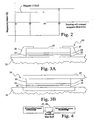
- permanent magnet 13 provides no bias magnetic field to the chip after tampering has occurred with respect to enclosure 10 that is sufficient to remove cover 12, and so permanent magnet 13, from the remainder of that enclosure or has otherwise separated magnet 13 and chip 14 so that no significant magnetic field from that magnet remains about that chip. Tamper detection in this configuration requires that the antitampering magnetoresistive sensing memory storage cell or cells have a magnetoresistance versus applied magnetic field characteristic which is offset with respect to the applied magnetic field axis as shown in the graph provided in Figure 2 .
- the antitampering magnetoresistive sensing memory cell magnetoresistance versus the sensor cell applied magnetic field characteristic is offset by 50 Oe along the positive applied field axis, and a permanent magnet is indicated to be providing a positive magnetic bias field having a value of 50 Oe.
- Detection of tampering with the enclosure takes place, for example, by having a maximum cell magnetoresistance value as a binary state "1" that is initially set in the cell using the chip data storage circuitry, and then having a minimum cell magnetoresistance value as a binary state "0" state that is subsequently found in the cell when it is later interrogated to check on whether an intrusion has occurred.
- a binary state "0" state determined to be present in the cell by the cell data retrieval circuitry will have occurred as a result of enclosure cover 12 with permanent magnet 13 having been removed by the tampering activity to thereby gain access to the interior of enclosure 10 containing protected chip 14 including the tampering detection magnetoresistive sensing memory storage cell or cells.
- the device In the absence of occurrences of external random direction magnetic fields affecting the antitampering sensing memory storage cell, the device is stable in having the smaller value switching threshold always remain between a slightly positive value field and a field of a value equal to 50 Oe. If magnet 13 is moved away from the sensing memory cell, then the bias magnetic field about the antitampering memory storage cell would be zero and the cell would go to the low resistance, or "0", state.
- the sensor cell could withstand an external applied random direction magnetic field with a component along the cell sensitive axis of a value up to 25 Oe and still detect a tamper with the enclosure that was sufficient to remove cover 12 from enclosure 10.
- Magnetoresistive memory storage cells having a relatively "square” magnetoresistance versus applied magnetic field characteristics are commonly observed in cells based on either “spin valve” or “spin tunneling” devices. Such characteristics provide relatively abrupt switching between alternative binary resistance value states, that is, the storage cell switches between a "0" state and a “1” state, or vice verse, over a very small range of values of an externally applied magnetic field.
- Layer diagrams representing basic schematic representations of such devices are shown in Figure 3 , a spin valve device being shown in Figure 3A and a magnetic tunneling junction device, or spin dependent tunneling device, being shown in Figure 3B .
- a spin valve device, 20, is supported on a substrate, 21, through having a first ferromagnetic material layer, 22, or “free” layer, shown on that substrate and supporting a layer of copper, 23, thereon which in turn supports thereon a second ferromagnetic material layer, 24, or “pinned” layer.
- An antiferromagnet, 25, is provided on pinned layer 24, and a pair of electrodes, 26 and 27, with each member of the pair at a corresponding opposite end of the foregoing sequence of layers provides the electrical interconnections for introducing current flows therebetween parallel to the main extent of the layer sequence.
- a spin dependent tunneling device, 30, in Figure 3B is supported on a substrate, 31, through having a first ferromagnetic material layer, 32, or “free” layer, shown on that substrate and supporting a layer of aluminum oxide, 33, thereon which in turn supports thereon a second ferromagnetic material layer, 34, or "pinned” layer.
- An antiferromagnet, 35 is provided on pinned layer 34, and a pair of electrodes, 36 and 37, with each member of the pair at a corresponding opposite side of the foregoing sequence of layers provides the electrical interconnections for introducing current flows therebetween perpendicular to the main extent of the layer sequence.
- antiferromagnetic layers 25 and 35 are each provided to maintain the magnetization direction of, or "pinning", of the corresponding one of pinned layers 24 and 34 so that the magnetization direction thereof does not react, or change significantly, in response to the expected values of the operating magnetic fields to be used in operating these devices.
- Corresponding "free" layers 22 and 32 are each relatively free to react to expected values of the operating magnetic fields through rotating their magnetization directions.
- Both of spin valve device 20 and magnetic tunnel junction 30 of Figures 3A and 3B can be provided so as to have magnetoresistance versus applied magnetic field characteristics that are closely approximated by the "square" loop shown in the graph of Figure 2 provided that the corresponding free layers are homogeneous and relatively smooth. The degree of offset in such characteristics along the applied field axis depends on several factors:
- orange peel coupling and indirect exchange coupling can offset one another in basic spin valve configuration 20 of Figure 3A to provide a low offset characteristic as required for some kinds of tampering cells.
- Providing a more complex pinning layer for magnetic tunneling junction structure 30 of Figure 3B can be done so as to also provide a low offset characteristic.
- either of the devices shown in Figures 3A and 3B can be biased to form an characteristic offset by setting the magnetization in other device structures positioned near to the Figures 3A and 3B devices to be biased. That is, a spin valve or magnetic tunnel junction cell can be placed between two permanently magnetized bodies or masses to provide a biasing magnetic field in the cell. The stray fields from the magnetizations in those devices together provide a resulting magnetic bias field, as shown in a representative configuration in Figure 4 , thus giving selectively either a small cell characteristic offset value or a relatively large characteristic offset value depending on the magnitude of the fields provided by those masses.
- the configuration shown in Figure 4 can be implemented in alternative manners.
- the magnetized masses on either side of a antitampering magnetoresistive sensing memory storage cell could be ferromagnetic films pinned by antiferromagnets in the direction shown.
- the magnetized films importantly must not change significantly in the presence of an external field, i.e. they must behave like permanent magnets.
- FIG. 5 shows some top views of alternative layout configurations for a spin valve cell with the cell layout in Figure 5A having blunt ends, the cell layout in Figure 5B having symmetrically tapered ends, and the cell layout in Figure 5C having asymmetrically tapered ends. Electrical circuitry contacts to the cells are represented by open rectangles within the outer edges of the cells in each of these figures.
- Sensing currents are passed through cells using the electrical circuit contacts therein as the basis for determining the electrical resistance thereof, and so to thereby obtain which resistive value logic state the cell is presently in, and such passing of current through spin valves also has the effect of reducing the cell magnetic field switching threshold value magnitudes.
- Forming the cell electrical circuitry contacts must be done so as to avoid etching or diffusion into the magnetic film layer as discontinuities in the film can serve as nucleation points for the formation of reverse domains.
- the cell structures shown in Figures 5B and 5C are desirable when the width of the spin valve devices or the magnetic tunnel junction devices is on the order of a few microns.
- selected initial cell states i.e. data
- an antitampering magnetoresistive sensing memory storage cell or possibly a group of such cells, in such a manner that, for a protected enclosure which has not been sufficiently tampered with to gain access to the interior thereof, results in the initially stored cell states, or the stored data, remaining unchanged.
- the detection of an intrusion sufficient to gain access to the interior of the protected enclosure involves having some mechanism present with the enclosure that leads to the magnetic field about the antitampering memory storage cell or cells changing when an intrusion occurs and, correspondingly, the antitampering memory storage cell, or at least some of a group of such cells, must responsively change to a state different than the initial state or states thereof if the occurrence of such an intrusion is to be recorded therein. Furthermore, simply returning the enclosure associated magnetic field changing mechanism to its original state must not reset the antitampering memory storage cell or cells to their initial states because there would then be no record of the intrusion in those cells.
- FIG. 6 An arrangement which allows differential measurement of antitampering memory storage cell resistance values for checking on the relative status of cell states in determining the occurrences of recordings of any serious intrusions into the enclosure, rather than measuring the absolute resistance value difference between different cell states to do so, as was indicated above, is shown in Figure 6 .
- enclosure arrangement 10"' (just partially shown) with again therein monolithic integrated circuit chip 14 on printed circuit board 15 (just partially shown) having antitampering magnetoresistive sensing memory storage cell 16 therein and permeable material shield 17 closely adjacent thereto.
- Enclosure 10"' has cover 12 (just partially shown) that goes over receptacle 11 (just partially shown) with a bottom and sides formed about an interior space, and the sides meet the cover to thereby deny access to printed circuit board 15 positioned in this interior space with chip 14 therein when cover 12 with magnet 13 embedded therein is in place against the upper ends of those receptacle sides.
- This arrangement is much like that of Figure 1 except that two antitampering magnetoresistive sensing memory storage cells 16 and 18 are shown provided in chip 14 that is itself separated from the item being protected, i.e. printed circuit board 15 and the other circuit element provided thereon.
- cell 16 has an initial "1" state stored therein and cell 18 has an initial "0" state stored therein through, in both instances, the use of data storage circuitry in the chip containing an on-chip coil, then these cells will retain these stored states under normal conditions with the cover and the magnetic attached thereto being in place against the base. Furthermore, if the cells are fabricated to be well matched and the cell resistances are measured with these initial state conditions, there will be a resistance difference measured between them. If, on the other hand, the cover is removed from the base because of tampering, and thus from being over the enclosure interior space so as to also remove the magnetic material shield from that space, then both cells will be in a "0" state in accord with the description associated with Figure 2 above. Such a tampering leading to the removal of the cover can then be detected by measuring the resistances of each cell which will, in this circumstance, be substantially equal for well matched cells.
- both cells When an external magnetic field less than the magnetic field switching threshold of either device is applied along the long dimension of the cells jointly both cells will then be magnetized in the same direction.
- a small field with respect to these cells occurs when the cover is removed from the enclosure, or when circuit board is removed from the enclosure in some other manner, as the magnet material shield will then no longer shield the cells from the magnetic field provided by the permanent magnet. That absence of a field through both cells will switch them both into the same state, and so the tampering with the enclosed the circuit board can be detected by noting the cell states even if the cover or the board or both have been returned to their initial positions. These subsequent measurements comparing the resistances of the two cells will thus show them to be about equal resistance and so in the same states, and thus a previous tampering is thereby detected.
- an entire magnetoresistive memory cell monolithic integrated circuit chip could be formed with such cells with this chip being positioned in the interior space of the enclosure. Then a tampering sufficient to remove the enclosure cover or to remove that chip from the enclosure in some other manner would result in the entire contents of the memory chip being erased because all of the cells in the memory would be set to the same state after such a tampering.
- microprocessor operated systems or microprocessor enabled systems
- such an erasure resulting from such tampering will prevent operating or enabling the associated system until the memory is reprogrammed.
- Memory cells based on spin valve devices or spin tunneling junction devices have an advantage over other kinds of magnetic memories because the erasure of the data, or states, initially stored therein is complete, i.e. the data cannot be reconstructed even following very careful analysis of the erased memory.
- a Code Select input is provided for selecting a particular stored code register arrangement for retrieval of the data stored therein or for storing some alternative data therein through modifying the previously set states in some or all of the cells.
- the code sequences could range from as few as 1 bit to as many as 10 kbits in length, and would be retrieved or stored through serial data input and output pins.
- a Tamper Detect output is provided as the point to obtain a signal indication that an enclosure tampering event has been detected. Such a tampering indication signal could be used to activate certain analog hardware or as a microprocessor interrupt in a microprocessor based system.
- An algorithm for generating a Tamper Detect output tampering occurrence signal could be based on the occurrence of some desired fraction of the cells in the selected code register arrangement all being in a common state resulting from all being set in the direction of magnetic field generated by the on-chip magnet, or based on a comparison between two register arrangements. Different versions of such memories or different versions of inputs to select the tamper detect algorithm make this configuration very flexible.
- the device of Figure 8 provides codewords directing operation or enablement, or both, of the associated system as serial data sequences, or perhaps just representing secret stored information for the user, and the memory is programmed from an input serial data sequence.
- Input signals to the Code Select input directs the hardware to select one of several codes stored in the secure memory device.
- a discrete output signal at the Tamper Detect output can be chosen, for example, to go to a high logic state when all of the bits in the selected codeword are the same, i.e. when the magnetizations of the corresponding cells in the memory have all been forced into the same direction by the magnetic field provided by the on-chip permanent magnet as a result of the enclosure cover having been removed from the enclosure base during a tampering.
- the regions marked Magnet pole at the top and bottom of the memory chip in Figure 8 are the magnetic poles that protrude through the top of the device encapsulating material much like the poles shown in Figure 1 although this is not the only magnet configuration possible for this purpose in some of which such poles would not be present.
Claims (15)
- Manipulationsfeststellende Gehäuseanordnung für einen umschlossenen Raum (10, 10', 10", 10"'), die einen Innenraum enthält, in dem ein geschütztes Objekt (14) positioniert ist, wobei die Anordnung Folgendes umfasst:eine Speicherzelle mit magnetoresistiver Erfassung (16) in oder nahe bei dem geschützten Objekt (14) in dem umschlossenen Raum (10, 10', 10", 10"') positioniert ist, die eine Charakteristik (13) eines Magnetwiderstandes über einem extern angelegten Magnetfeld mit ersten und zweiten Zuständen von verschiedenen Widerstandswerten hat, wobei die Speicherzelle dafür ausgelegt ist, aus dem ersten Zustand in den zweiten Zustand bei Vorliegen einer Magnetfeldgröße überzugehen, die kleiner als ein erster Schwellwert-Magnetfeldwert ist, und wobei die Speicherzelle anfänglich dafür ausgelegt ist, im ersten Zustand beschrieben zu werden, wenn sie in oder nahe bei dem geschützten Objekt im umschlossenen Raum positioniert ist, undein Magnet (13), der in einem ausgewählten anfänglichen Trennungsabstand von der Speicherzelle mit magnetoresistiver Erfassung (16) positioniert ist, um damit für ein Magnetfeld einer Anfangsgröße für die Speicherzelle mit magnetoresistiver Erfassung zu sorgen, die zwischen dem ersten Schwellwert-Magnetfeldwert und einem zweiten Schwellwert-Magnetfeldwert liegt, wobei das Magnetfeld sich unter den ersten Schwellwert-Magnetfeldwert verringert, wenn der umschlossene Raum (10, 10', 10", 10"') geöffnet wird, was zu einer beträchtlichen Vergrößerung eines Abstandes zwischen dem Magneten (13) und der Speicherzelle mit magnetoresistiver Erfassung (16) und damit der Öffnung des Trennungsabstandes führt, der größer als der anfängliche Trennungsabstand ist,dadurch gekennzeichnet, dass die Speicherzelle vom zweiten Zustand in den ersten Zustand bei Vorhandensein einer Magnetfeldgröße übergeht, die größer als der zweite Schwellwert-Magnetfeldwert ist, wobei der zweite Schwellwert-Magnetfeldwert größer als der erste Schwellwert-Magnetfeldwert ist.
- Anordnung nach Anspruch 1, wobei der umschlossene Raum (10, 10', 10", 10"') einen Aufnahmebehälter (11) mit zumindest einem Teil des Innenraums darin und eine Abdeckung (12) hat, die so positioniert werden kann, dass der Innenraum vom umschlossenen Raum umgeben ist.
- Anordnung nach Anspruch 1, wobei die Speicherzelle mit magnetoresistiver Erfassung (16) in einer monolithischen integrierten Schaltung (14) gebildet ist, welche sich im Innenraum befindet.
- Anordnung nach Anspruch 1, die ferner einen Teil einer Schicht des magnetisch permeablen Materials (17) umfasst, welches der Speicherzelle mit magnetoresistiver Erfassung (16) benachbart ist.
- Anordnung nach Anspruch 1, die ferner eine andere Speicherzelle mit magnetoresistiver Erfassung (18) umfasst, welche in oder nahe beim geschützten Objekt (14) im umschlossenen Raum (10, 10', 10", 10"') positioniert ist, welche eine Charakteristik eines Magnetwiderstandes über einem extern angelegten Feld mit erstem und zweitem Zustand von unterschiedlichen Widerstandswerten hat, wobei die Speicherzelle (18) vom ersten Zustand in den zweiten Zustand in Gegenwart einer Magnetfeldgröße übergeht, die kleiner als ein erster Schwellwert-Magnetfeldwert ist, und vom zweiten Zustand in den ersten Zustand in Gegenwart eines Magnetfeldwertes übergeht, der größer als zweiter Schwellwert-Magnetfeldwert ist, wobei der zweite Schwellwert-Magnetfeldwert größer als der erste Schwellwert-Magnetfeldwert ist und wobei die Speicherzelle (18) anfänglich im zweiten Zustand beschrieben wird, wenn sie in oder nahe bei dem geschützten Objekt im umschlossenen Raum positioniert ist.
- Anordnung nach Anspruch 1, wobei die Speicherzelle mit magnetoresistiver Erfassung (16) eine Länge entlang einer gewählten Richtung und eine Breite hat, die im Wesentlichen senkrecht dazu ist, welche eine geringere Ausdehnung als die Länge hat und die zusammen einen geformten Endteil haben, der sich über einen Teil der Länge erstreckt, in der sich die Breite allmählich am Ende derselben auf null reduziert.
- Anordnung nach Anspruch 2, wobei der Magnet (13) in der Abdeckung (12) positioniert ist.
- Anordnung nach Anspruch 5, wobei das Magnetfeld von anfänglicher Größe, das vom Magneten (13) bereitgestellt wird, für beide Speicherzellen mit magnetoresistiver Erfassung (16, 18) bereitgestellt wird.
- Anordnung nach Anspruch 8, die ferner einen Leiter umfasst, der nahe bei den Speicherzellen mit magnetoresistiver Erfassung (16, 18) derart aufgewickelt ist, dass jeder elektrische Strom, der durch den Leiter fließt, dazu tendiert, sie in den entgegengesetzten Widerstandswertzustand zu versetzen.
- Anordnung nach Anspruch 1, wobei die Speicherzelle mit magnetoresistiver Erfassung (16) einen magnetisierten Körper hat, der in der Nähe derselben angeordnet ist.
- Anordnung nach Anspruch 1, wobei der umschlossene Raum (10, 10', 10", 10"') durch einen Körper aus elektrisch isolierendem, festen Material gebildet ist, wobei der Innenraum auf das darin Eingeschlossene beschränkt ist, was die Speicherzelle mit magnetoresistiver Erfassung (16) und den Magneten (13) umfasst.
- Anordnung nach Anspruch 11, die ferner einen Teil einer Schicht des magnetisch permeablen Materials (17) umfasst, welches der Speicherzelle mit magnetoresistiver Erfassung (16) benachbart ist.
- Anordnung nach Anspruch 11, die ferner eine weitere Speicherzelle mit magnetoresistiver Erfassung (18) umfasst, welche in oder nahe bei dem geschützten Objekt (14) im umschlossenen Raum (10, 10', 10", 10"') positioniert ist, die eine Charakteristik eines Magnetwiderstandes über einem extern angelegten Feld mit erstem und zweitem Zustand von unterschiedlichen Widerstandswerten hat, wobei die Speicherzelle (18) vom ersten Zustand in den zweiten Zustand in Gegenwart einer Magnetfeldgröße übergeht, die kleiner als ein erster Schwellwert-Magnetfeldwert ist, und vom zweiten Zustand in den ersten Zustand in Gegenwart eines Magnetfeldwertes übergeht, der größer als ein zweiter Schwellwert-Magnetfeldwert ist, wobei der zweite Schwellwert-Magnetfeldwert größer als der erste Schwellwert-Magnetfeldwert ist und wobei die Speicherzelle (18) anfänglich im zweiten Zustand beschrieben wird, wenn sie in oder nahe bei dem geschützten Objekt im umschlossenen Raum positioniert ist.
- Anordnung nach Anspruch 11, wobei die Speicherzelle mit magnetoresistiver Erfassung (16) eine Länge entlang einer gewählten Richtung und eine Breite hat, die im Wesentlichen senkrecht dazu ist, welche eine geringere Ausdehnung als die Länge hat und die zusammen einen geformten Endteil haben, der sich über einen Teil der Länge erstreckt, in der sich die Breite allmählich am Ende derselben auf null reduziert.
- Anordnung nach Anspruch 13, die ferner einen Leiter umfasst, der nahe bei den Speicherzellen mit magnetoresistiver Erfassung (16, 18) derart aufgewickelt ist, dass jeder elektrische Strom, der durch den Leiter fließt, dazu tendiert, sie in den entgegengesetzten Widerstandswertzustand zu versetzen.
Applications Claiming Priority (2)
| Application Number | Priority Date | Filing Date | Title |
|---|---|---|---|
| US79356906P | 2006-04-20 | 2006-04-20 | |
| PCT/US2007/009793 WO2007124129A2 (en) | 2006-04-20 | 2007-04-20 | Enclosure tamper detection and protection |
Publications (3)
| Publication Number | Publication Date |
|---|---|
| EP2016593A2 EP2016593A2 (de) | 2009-01-21 |
| EP2016593A4 EP2016593A4 (de) | 2011-08-03 |
| EP2016593B1 true EP2016593B1 (de) | 2014-11-05 |
Family
ID=38625655
Family Applications (1)
| Application Number | Title | Priority Date | Filing Date |
|---|---|---|---|
| EP07755879.9A Active EP2016593B1 (de) | 2006-04-20 | 2007-04-20 | Manipulationsdetektion und -schutz für gehäuse |
Country Status (3)
| Country | Link |
|---|---|
| US (1) | US7468664B2 (de) |
| EP (1) | EP2016593B1 (de) |
| WO (1) | WO2007124129A2 (de) |
Families Citing this family (17)
| Publication number | Priority date | Publication date | Assignee | Title |
|---|---|---|---|---|
| EP1576613B1 (de) * | 2002-12-18 | 2014-06-18 | Crocus Technology Inc. | Verfahren und vorrichtung zum schutz einer mram-vorrichtung gegen angriffe |
| GB2412996B (en) * | 2004-04-08 | 2008-11-12 | Gore & Ass | Tamper respondent covering |
| US20070279969A1 (en) * | 2006-06-02 | 2007-12-06 | Raytheon Company | Intrusion detection apparatus and method |
| US7948378B2 (en) * | 2008-10-06 | 2011-05-24 | Toptech Systems, Inc. | Tamperproof non-contact switch |
| US9041388B2 (en) * | 2009-07-27 | 2015-05-26 | Iii Holdings 3, Llc | Non-contact current sensor |
| KR101841130B1 (ko) * | 2010-06-22 | 2018-03-22 | 스토라 엔소 오와이제이 | 섬유 또는 플라스틱 기반 패키지, 그 섬유 또는 플라스틱 기반 패키지에 의한 무선 데이터 통신을 위한 장치, 방법, 프로그램 및 시스템 |
| CN102226836A (zh) * | 2011-04-06 | 2011-10-26 | 江苏多维科技有限公司 | 单一芯片桥式磁场传感器及其制备方法 |
| US8854870B2 (en) | 2012-03-13 | 2014-10-07 | Honeywell International Inc. | Magnetoresistive random access memory (MRAM) die including an integrated magnetic security structure |
| US8811072B2 (en) * | 2012-03-13 | 2014-08-19 | Honeywell International Inc. | Magnetoresistive random access memory (MRAM) package including a multilayer magnetic security structure |
| US8909942B1 (en) | 2012-03-30 | 2014-12-09 | Western Digital Technologies, Inc. | MRAM-based security for data storage systems |
| US20140184411A1 (en) * | 2012-12-31 | 2014-07-03 | Alcatel Lucent | Alarm condition processing in network element |
| CN106781144B (zh) * | 2015-11-11 | 2020-07-10 | 迈来芯科技有限公司 | 磁传感器 |
| EP3226017B1 (de) | 2016-03-31 | 2018-10-24 | Siemens Aktiengesellschaft | Detektion eines öffnungsvorganges einer abdeckvorrichtung |
| EP3226018B1 (de) | 2016-03-31 | 2018-11-07 | Siemens Aktiengesellschaft | Detektion eines öffnungsvorganges einer abdeckvorrichtung |
| US10489614B2 (en) | 2017-09-26 | 2019-11-26 | Hewlett Packard Enterprise Development Lp | Tamper detecting cases |
| US11685580B2 (en) * | 2019-08-07 | 2023-06-27 | International Business Machines Corporation | Medication counterfeit detection |
| FR3111737B1 (fr) * | 2020-06-19 | 2022-07-08 | Commissariat Energie Atomique | Protection de puce ou de boitier-systeme utilisant l’effet gmi |
Family Cites Families (37)
| Publication number | Priority date | Publication date | Assignee | Title |
|---|---|---|---|---|
| US3971916A (en) | 1974-03-25 | 1976-07-27 | Societe Internationale | Methods of data storage and data storage systems |
| CA1145008A (en) * | 1980-01-22 | 1983-04-19 | Ezequiel Mejia | Intrusion detecting switch |
| GB2071333B (en) * | 1980-02-22 | 1984-02-01 | Sony Corp | Magnetic sensor device |
| US4860351A (en) * | 1986-11-05 | 1989-08-22 | Ibm Corporation | Tamper-resistant packaging for protection of information stored in electronic circuitry |
| US5117457A (en) * | 1986-11-05 | 1992-05-26 | International Business Machines Corp. | Tamper resistant packaging for information protection in electronic circuitry |
| US5027397A (en) | 1989-09-12 | 1991-06-25 | International Business Machines Corporation | Data protection by detection of intrusion into electronic assemblies |
| US5233505A (en) * | 1991-12-30 | 1993-08-03 | Yeng-Ming Chang | Security device for protecting electronically-stored data |
| US5602381A (en) | 1993-05-19 | 1997-02-11 | Nhk Spring Co., Ltd. | Objects to be checked for authenticity, and method and apparatus for checking whether or not objects are authentic |
| US5675319A (en) * | 1996-04-26 | 1997-10-07 | David Sarnoff Research Center, Inc. | Tamper detection device |
| US5790670A (en) | 1996-07-18 | 1998-08-04 | Citicorp Development Center, Inc. | Apparatus and method for securing electronic circuitry |
| US5910774A (en) | 1996-09-18 | 1999-06-08 | Itron, Inc. | Sensor for count and tamper detection |
| JP3440763B2 (ja) | 1996-10-25 | 2003-08-25 | 富士ゼロックス株式会社 | 暗号化装置、復号装置、機密データ処理装置、及び情報処理装置 |
| US6547364B2 (en) | 1997-07-12 | 2003-04-15 | Silverbrook Research Pty Ltd | Printing cartridge with an integrated circuit device |
| GB9809810D0 (en) | 1998-05-07 | 1998-07-08 | Redcliffe Magtronics Limited | Improvements relating to tamper proof closures |
| EP0964361A1 (de) | 1998-06-08 | 1999-12-15 | International Business Machines Corporation | In integrierten Chipkarten enthaltene Absicherung empfindlicher Information |
| US6816968B1 (en) | 1998-07-10 | 2004-11-09 | Silverbrook Research Pty Ltd | Consumable authentication protocol and system |
| US6501390B1 (en) | 1999-01-11 | 2002-12-31 | International Business Machines Corporation | Method and apparatus for securely determining aspects of the history of a good |
| US6774807B1 (en) | 1999-03-02 | 2004-08-10 | Cadence Design Systems, Inc. | Tamper detection mechanism |
| SE522531C2 (sv) | 1999-11-24 | 2004-02-17 | Micronic Laser Systems Ab | Metod och anordning för märkning av halvledare |
| US6784796B2 (en) * | 1999-12-17 | 2004-08-31 | The Regents Of The University Of Califronia | Magnetic vector field tag and seal |
| US7005733B2 (en) | 1999-12-30 | 2006-02-28 | Koemmerling Oliver | Anti tamper encapsulation for an integrated circuit |
| WO2001051949A1 (en) * | 2000-01-13 | 2001-07-19 | Seagate Technology Llc | Dual spin-valve magnetoresistive sensor |
| DE10010457A1 (de) * | 2000-03-03 | 2001-09-20 | Infineon Technologies Ag | Integrierter Speicher mit Speicherzellen mit magnetoresistivem Speichereffekt |
| US6310549B1 (en) | 2000-08-29 | 2001-10-30 | Digitech International | Wireless security system |
| US6891474B1 (en) | 2001-08-01 | 2005-05-10 | Tagsense, Inc. | Electromagnetic identification label for anti-counterfeiting, authentication, and tamper-protection |
| JP2003331241A (ja) | 2002-05-09 | 2003-11-21 | Fujitsu Ltd | メモリデバイス及びその制御方法 |
| US6778083B2 (en) | 2002-08-27 | 2004-08-17 | Hi-G-Tek Ltd. | Electronic locking seal |
| US6753775B2 (en) | 2002-08-27 | 2004-06-22 | Hi-G-Tek Ltd. | Smart container monitoring system |
| DE60331682D1 (de) * | 2002-12-18 | 2010-04-22 | Nxp Bv | Betrugssichere verpackung |
| CN1729541A (zh) | 2002-12-18 | 2006-02-01 | 皇家飞利浦电子股份有限公司 | 抗窜改封装和方法 |
| US7712147B2 (en) | 2002-12-18 | 2010-05-04 | Nxp B.V. | Method and device for protection of an mram device against tampering |
| US7224634B2 (en) | 2002-12-18 | 2007-05-29 | Nxp B.V. | Hardware security device for magnetic memory cells |
| DE602004022915D1 (de) | 2003-01-14 | 2009-10-15 | Nxp Bv | Manipulationsbeständige kapselung und ansatz mit magnetischgesetzten daten |
| GB2397272B (en) | 2003-01-15 | 2006-11-15 | Hewlett Packard Co | Secure physical documents and methods and apparatus for publishing and reading them |
| US7017807B2 (en) | 2003-09-08 | 2006-03-28 | Francis M. Claessens | Apparatus and method for detecting tampering with containers and preventing counterfeiting thereof |
| EP1617472A1 (de) * | 2004-07-16 | 2006-01-18 | Axalto SA | Eine aktive Schutzanordnung zum Schutz einer Schaltung gegenüber mechanischem- und elektromagnetischem Angriff |
| US7151461B2 (en) * | 2004-10-29 | 2006-12-19 | Honeywell International, Inc. | Magnetic contact tamper switch for security accessories |
-
2007
- 2007-04-20 EP EP07755879.9A patent/EP2016593B1/de active Active
- 2007-04-20 US US11/788,616 patent/US7468664B2/en active Active
- 2007-04-20 WO PCT/US2007/009793 patent/WO2007124129A2/en active Application Filing
Also Published As
| Publication number | Publication date |
|---|---|
| US20080042834A1 (en) | 2008-02-21 |
| EP2016593A4 (de) | 2011-08-03 |
| WO2007124129A3 (en) | 2009-04-09 |
| EP2016593A2 (de) | 2009-01-21 |
| US7468664B2 (en) | 2008-12-23 |
| WO2007124129A2 (en) | 2007-11-01 |
Similar Documents
| Publication | Publication Date | Title |
|---|---|---|
| EP2016593B1 (de) | Manipulationsdetektion und -schutz für gehäuse | |
| US8261367B2 (en) | Method and device for protection of an MRAM device against tampering | |
| US9030200B2 (en) | Spin dependent tunneling devices with magnetization states based on stress conditions | |
| EP1576611B1 (de) | Manipulationssicheres gehäuse für integrierte schaltkreise und verfahren | |
| US7791920B2 (en) | Active shielding for a circuit comprising magnetically sensitive materials | |
| EP1588371B1 (de) | Manipulationsbeständige kapselung und ansatz mit magnetischgesetzten daten | |
| US7712147B2 (en) | Method and device for protection of an mram device against tampering | |
| US8167057B2 (en) | Intrusion resistant apparatus and method | |
| EP1576614B1 (de) | Betrugssichere verpackung | |
| US7224634B2 (en) | Hardware security device for magnetic memory cells | |
| EP1690261B1 (de) | Verfahren und einrichtung zur verhinderung einer falschen programmierung eines magnetoresistiven speicherelements | |
| KR20050048667A (ko) | 판독전용 자기 메모리장치 엠알오엠 | |
| EP1576615B1 (de) | Hardwaresicherheitseinrichtung für magnetspeicherzellen |
Legal Events
| Date | Code | Title | Description |
|---|---|---|---|
| PUAI | Public reference made under article 153(3) epc to a published international application that has entered the european phase |
Free format text: ORIGINAL CODE: 0009012 |
|
| 17P | Request for examination filed |
Effective date: 20081120 |
|
| AK | Designated contracting states |
Kind code of ref document: A2 Designated state(s): AT BE BG CH CY CZ DE DK EE ES FI FR GB GR HU IE IS IT LI LT LU LV MC MT NL PL PT RO SE SI SK TR |
|
| AX | Request for extension of the european patent |
Extension state: AL BA HR MK RS |
|
| R17D | Deferred search report published (corrected) |
Effective date: 20090409 |
|
| RIC1 | Information provided on ipc code assigned before grant |
Ipc: G08B 21/00 20060101ALI20090611BHEP Ipc: G08B 13/08 20060101AFI20090611BHEP |
|
| DAX | Request for extension of the european patent (deleted) | ||
| RBV | Designated contracting states (corrected) |
Designated state(s): DE GB |
|
| A4 | Supplementary search report drawn up and despatched |
Effective date: 20110630 |
|
| RIC1 | Information provided on ipc code assigned before grant |
Ipc: G01R 33/00 20060101ALI20110624BHEP Ipc: G08B 21/00 20060101ALI20110624BHEP Ipc: G08B 13/08 20060101AFI20090611BHEP |
|
| REG | Reference to a national code |
Ref country code: DE Ref legal event code: R079 Ref document number: 602007039149 Country of ref document: DE Free format text: PREVIOUS MAIN CLASS: G11C0019080000 Ipc: G08B0013080000 |
|
| GRAP | Despatch of communication of intention to grant a patent |
Free format text: ORIGINAL CODE: EPIDOSNIGR1 |
|
| RIC1 | Information provided on ipc code assigned before grant |
Ipc: G08B 13/08 20060101AFI20140513BHEP Ipc: G08B 21/00 20060101ALI20140513BHEP Ipc: G01R 33/00 20060101ALI20140513BHEP |
|
| INTG | Intention to grant announced |
Effective date: 20140602 |
|
| GRAS | Grant fee paid |
Free format text: ORIGINAL CODE: EPIDOSNIGR3 |
|
| GRAA | (expected) grant |
Free format text: ORIGINAL CODE: 0009210 |
|
| AK | Designated contracting states |
Kind code of ref document: B1 Designated state(s): DE GB |
|
| REG | Reference to a national code |
Ref country code: GB Ref legal event code: FG4D |
|
| REG | Reference to a national code |
Ref country code: DE Ref legal event code: R096 Ref document number: 602007039149 Country of ref document: DE Effective date: 20141218 |
|
| REG | Reference to a national code |
Ref country code: DE Ref legal event code: R097 Ref document number: 602007039149 Country of ref document: DE |
|
| PLBE | No opposition filed within time limit |
Free format text: ORIGINAL CODE: 0009261 |
|
| STAA | Information on the status of an ep patent application or granted ep patent |
Free format text: STATUS: NO OPPOSITION FILED WITHIN TIME LIMIT |
|
| 26N | No opposition filed |
Effective date: 20150806 |
|
| REG | Reference to a national code |
Ref country code: DE Ref legal event code: R082 Ref document number: 602007039149 Country of ref document: DE |
|
| PGFP | Annual fee paid to national office [announced via postgrant information from national office to epo] |
Ref country code: DE Payment date: 20230320 Year of fee payment: 17 |
|
| PGFP | Annual fee paid to national office [announced via postgrant information from national office to epo] |
Ref country code: GB Payment date: 20240314 Year of fee payment: 18 |