EP2014143B1 - Conductive polymer electronic devices with surface mountable configuration and methods for manufacturing same - Google Patents
Conductive polymer electronic devices with surface mountable configuration and methods for manufacturing same Download PDFInfo
- Publication number
- EP2014143B1 EP2014143B1 EP07760729.9A EP07760729A EP2014143B1 EP 2014143 B1 EP2014143 B1 EP 2014143B1 EP 07760729 A EP07760729 A EP 07760729A EP 2014143 B1 EP2014143 B1 EP 2014143B1
- Authority
- EP
- European Patent Office
- Prior art keywords
- layer
- cross
- electrode
- insulation layer
- electrodes
- Prior art date
- Legal status (The legal status is an assumption and is not a legal conclusion. Google has not performed a legal analysis and makes no representation as to the accuracy of the status listed.)
- Active
Links
Images







Classifications
-
- H—ELECTRICITY
- H01—ELECTRIC ELEMENTS
- H01C—RESISTORS
- H01C7/00—Non-adjustable resistors formed as one or more layers or coatings; Non-adjustable resistors made from powdered conducting material or powdered semi-conducting material with or without insulating material
- H01C7/02—Non-adjustable resistors formed as one or more layers or coatings; Non-adjustable resistors made from powdered conducting material or powdered semi-conducting material with or without insulating material having positive temperature coefficient
- H01C7/021—Non-adjustable resistors formed as one or more layers or coatings; Non-adjustable resistors made from powdered conducting material or powdered semi-conducting material with or without insulating material having positive temperature coefficient formed with two or more layers
-
- H—ELECTRICITY
- H01—ELECTRIC ELEMENTS
- H01C—RESISTORS
- H01C1/00—Details
- H01C1/14—Terminals or tapping points specially adapted for resistors; Arrangements of terminals or tapping points on resistors
- H01C1/1406—Terminals or electrodes formed on resistive elements having positive temperature coefficient
-
- H—ELECTRICITY
- H01—ELECTRIC ELEMENTS
- H01C—RESISTORS
- H01C1/00—Details
- H01C1/14—Terminals or tapping points specially adapted for resistors; Arrangements of terminals or tapping points on resistors
- H01C1/1413—Terminals or electrodes formed on resistive elements having negative temperature coefficient
-
- H—ELECTRICITY
- H01—ELECTRIC ELEMENTS
- H01C—RESISTORS
- H01C17/00—Apparatus or processes specially adapted for manufacturing resistors
- H01C17/02—Apparatus or processes specially adapted for manufacturing resistors adapted for manufacturing resistors with envelope or housing
-
- H—ELECTRICITY
- H01—ELECTRIC ELEMENTS
- H01C—RESISTORS
- H01C17/00—Apparatus or processes specially adapted for manufacturing resistors
- H01C17/28—Apparatus or processes specially adapted for manufacturing resistors adapted for applying terminals
- H01C17/281—Apparatus or processes specially adapted for manufacturing resistors adapted for applying terminals by thick film techniques
-
- H—ELECTRICITY
- H01—ELECTRIC ELEMENTS
- H01C—RESISTORS
- H01C7/00—Non-adjustable resistors formed as one or more layers or coatings; Non-adjustable resistors made from powdered conducting material or powdered semi-conducting material with or without insulating material
- H01C7/003—Thick film resistors
- H01C7/005—Polymer thick films
-
- H—ELECTRICITY
- H01—ELECTRIC ELEMENTS
- H01C—RESISTORS
- H01C7/00—Non-adjustable resistors formed as one or more layers or coatings; Non-adjustable resistors made from powdered conducting material or powdered semi-conducting material with or without insulating material
- H01C7/02—Non-adjustable resistors formed as one or more layers or coatings; Non-adjustable resistors made from powdered conducting material or powdered semi-conducting material with or without insulating material having positive temperature coefficient
- H01C7/028—Non-adjustable resistors formed as one or more layers or coatings; Non-adjustable resistors made from powdered conducting material or powdered semi-conducting material with or without insulating material having positive temperature coefficient consisting of organic substances
-
- H—ELECTRICITY
- H01—ELECTRIC ELEMENTS
- H01C—RESISTORS
- H01C7/00—Non-adjustable resistors formed as one or more layers or coatings; Non-adjustable resistors made from powdered conducting material or powdered semi-conducting material with or without insulating material
- H01C7/04—Non-adjustable resistors formed as one or more layers or coatings; Non-adjustable resistors made from powdered conducting material or powdered semi-conducting material with or without insulating material having negative temperature coefficient
- H01C7/041—Non-adjustable resistors formed as one or more layers or coatings; Non-adjustable resistors made from powdered conducting material or powdered semi-conducting material with or without insulating material having negative temperature coefficient formed with two or more layers
-
- H—ELECTRICITY
- H01—ELECTRIC ELEMENTS
- H01C—RESISTORS
- H01C7/00—Non-adjustable resistors formed as one or more layers or coatings; Non-adjustable resistors made from powdered conducting material or powdered semi-conducting material with or without insulating material
- H01C7/18—Non-adjustable resistors formed as one or more layers or coatings; Non-adjustable resistors made from powdered conducting material or powdered semi-conducting material with or without insulating material comprising a plurality of layers stacked between terminals
-
- H—ELECTRICITY
- H01—ELECTRIC ELEMENTS
- H01C—RESISTORS
- H01C1/00—Details
- H01C1/01—Mounting; Supporting
- H01C1/016—Mounting; Supporting with compensation for resistor expansion or contraction
-
- H—ELECTRICITY
- H01—ELECTRIC ELEMENTS
- H01C—RESISTORS
- H01C7/00—Non-adjustable resistors formed as one or more layers or coatings; Non-adjustable resistors made from powdered conducting material or powdered semi-conducting material with or without insulating material
- H01C7/04—Non-adjustable resistors formed as one or more layers or coatings; Non-adjustable resistors made from powdered conducting material or powdered semi-conducting material with or without insulating material having negative temperature coefficient
- H01C7/049—Non-adjustable resistors formed as one or more layers or coatings; Non-adjustable resistors made from powdered conducting material or powdered semi-conducting material with or without insulating material having negative temperature coefficient mainly consisting of organic or organo-metal substances
-
- Y—GENERAL TAGGING OF NEW TECHNOLOGICAL DEVELOPMENTS; GENERAL TAGGING OF CROSS-SECTIONAL TECHNOLOGIES SPANNING OVER SEVERAL SECTIONS OF THE IPC; TECHNICAL SUBJECTS COVERED BY FORMER USPC CROSS-REFERENCE ART COLLECTIONS [XRACs] AND DIGESTS
- Y10—TECHNICAL SUBJECTS COVERED BY FORMER USPC
- Y10T—TECHNICAL SUBJECTS COVERED BY FORMER US CLASSIFICATION
- Y10T29/00—Metal working
- Y10T29/49—Method of mechanical manufacture
- Y10T29/49002—Electrical device making
- Y10T29/49117—Conductor or circuit manufacturing
- Y10T29/49124—On flat or curved insulated base, e.g., printed circuit, etc.
- Y10T29/49155—Manufacturing circuit on or in base
- Y10T29/49165—Manufacturing circuit on or in base by forming conductive walled aperture in base
Definitions
- This disclosure relates to the field of conductive polymer electronic components and devices.
- resistive devices comprising a layer of thermally-sensitive resistive material, such as a conductive polymer, that is laminated between a pair of planar electrodes, wherein the device has a surface-mountable configuration.
- Conductive polymer thermally-sensitive resistive devices have become commonplace on electronic circuits. These include devices that exhibit a positive temperature coefficient of resistivity (PTC) and a negative temperature coefficient of resistivity (NTC).
- PTC positive temperature coefficient of resistivity
- NTC negative temperature coefficient of resistivity
- resistive devices comprising a conductive polymer resistive material exhibiting a positive temperature coefficient of resistivity (PTC) have found widespread uses as over-current protection devices or "self-resettable fuses," due to their ability to undergo a rapid and drastic (at least three or four orders of magnitude) increase in resistance in response to an over-current situation.
- Conductive polymer PTC elements are typically formed from an organic polymer, such as polyethylene, into which is mixed conductive particles, such as carbon black or metallic particles.
- the conductivity (or, conversely, the resistivity) of the composition is determined, in substantial part, by the average spacing between the conductive particles.
- the drastic and sudden increase in resistivity of a conductive polymer element in a PTC device upon experiencing an over-current condition is due to a thermally-induced expansion of the polymer element, which increases the average spacing between the conductive particles within the polymeric material.
- the functionality of the device may be impaired, especially after repeated over-current "trippings.”
- “repeatability” the characteristic of the device to exhibit substantially the same operational parameters
- duty cycles over-current tripping and subsequent resetting upon removal of the overvoltage
- typical prior art conductive polymer PTC devices tend to exhibit poor resistance stability as a function of the number of duty cycles. This means that the normal (non-over-current condition) resistance in many prior art conductive polymer PTC devices tends to increase markedly after as few as 40-50 duty cycles. Furthermore, to the extent that the metal elements allow at least some degree of polymeric expansion, the metal elements are subject to mechanical stresses that may compromise the physical integrity of the device over repeated duty cycles.
- a surface-mountable conductive polymer electronic device in accordance with appended claim 1.
- a surface-mountable conductive polymer electronic device having multiple active layers of conductive polymeric material in accordance with appended claim 4. Specific embodiments of these general embodiments are recited in dependent claims 2-3 and 5-8.
- invention and “present invention” are to be understood as encompassing the invention described herein in accordance with the appended claims.
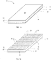
- a laminated sheet structure 10 comprises a layer of a polymeric active material 16 laminated between an upper laminar metal layer 12 and a lower laminar metal layer 14.
- the polymeric layer 16 may be a conductive polymer, such as a polymer that exhibits a positive temperature coefficient of resistivity, or it may be a polymeric dielectric material, or a ferromagnetic polymer.
- conductive polymer PTC materials are well-known in the art, some of which may include one or more of an anti-oxidant, a cross-linking agent, a coupling agent and a stabilizer.
- the metal layers 12, 14 are preferably made of conductive metal foil, and more preferably a nickel-plated copper foil that is nodularized (by conventional techniques) on the surface that is placed against the polymeric layer.
- the metal layers 12, 14 are of nodularized nickel-plated copper foil having a thickness of about 18 microns.
- the lamination may be performed by any suitable lamination process known in the art, an example of which is described in International Patent Publication No. WO 97/06660 .
- metallize directly the upper and lower surfaces of a sheet of polymeric material As an alternative to laminating a layer of polymeric material between upper and lower foil sheets, it may be advantageous, for certain applications, to metallize directly the upper and lower surfaces of a sheet of polymeric material.
- the metallization may be accomplished by a metal plating process, vapor deposition, screen-printing, or any other suitable process that may suggest itself to those skilled in the pertinent arts.
- the preferred embodiments of the present invention use the laminated structure described above, and the ensuing description will be based on the use of the lamination process.
- the upper and lower metal layers 12, 14 are photo-resist masked and etched to form electrodes (not shown in FIGS. 1A and 1B ).
- upper and lower insulation layers 18, 20 are applied to the upper and lower electrodes.
- a bottom metallization layer 22 (preferably copper) is applied to the lower insulation layer 20, and a top metallization layer 24 (also, preferably, copper) may optionally be applied to the upper insulation layer 18.
- the metallization layers 22, 24 are preferably in the form of copper foils, but they may also be applied by plating, vapor deposition, screen printing, or any other suitable process.
- the metallization layers are made of copper foil of about 18 microns in thickness.
- the insulation layers and the metallization layer or layers may be applied in separate steps.
- the lower insulation layer 20 and the bottom metallization layer 22 may be applied together as a pre-formed laminate, as may be the upper insulation 18 layer and the top metallization layer 24 (if present).
- an array of through-hole vias (not shown in FIGS. 1A and 1B ) is formed through the laminated structure 10 at appropriate locations.
- the bottom metallization layer 22 is photo-resist masked and etched to form surface-mount terminals (not shown in FIGS. 1A and 1B ), and the optional top metallization layer 24, if present, is photo-resist masked and etched to form anchor pads and (optionally) identifying indicia (not shown in FIGS. 1A and 1B ).
- the remaining exposed metal surfaces are plated with one or more solderable metals, such as nickel followed by gold, nickel followed by tin, or tin only.
- solderable metals such as nickel followed by gold, nickel followed by tin, or tin only.
- the plating with solderable metals may be performed immediately after the copper plating step, and before the etching of the metallization layer(s).
- the metallized vias form cross-conductors connecting each of the electrodes with one of the terminals.
- the laminated sheet structure 10 is typically sized to provide a matrix comprising a multitude of electronic devices.
- the sheet 10 may advantageously be provided with a grid of singulation lines 26 that are formed in or on the top-most and bottommost surface of the structure 10, and that define the perimeters of a plurality of devices 28.
- the singulation lines 26 may be formed by conventional photo-resist masking and etching techniques, and they are preferably of sufficient width to provide a small space or "isolation barrier" that is formed along the edges of each device 28 after singulation by a singulation device (not shown).
- the isolation barrier minimizes the probability of a short occurring between adjacent conductive elements (electrodes or terminals, as will be described) for which electrical isolation is desired.
- the singulation lines 26 may be "virtual" lines that form a virtual reference grid stored in the memory of a computerized singulation device, or that is otherwise created by the singulation device.
- the devices described below are advantageously mass-produced while interconnected in a matrix provided by a single laminated sheet structure 10 (for a single active layer device), or in a matrix formed by the lamination of two or more sheet structures into a multi-layer laminated structure (for a device having two or more active layers).
- the matrix is then singulated (e.g., along the lines 26) to form individual devices.
- the discussion below will be set forth with reference to the illustration of a single device, but it is to be understood that the process steps described below are performed on a matrix of such devices while they are interconnected in such a matrix. Thus, each step is performed simultaneously at a plurality of pre-defined locations on the matrix.
- the individual devices are separated from the matrix (singulated) by cutting, breaking, or dicing the matrix along the singulation lines 26, or along a grid of separation lines defined by the singulation apparatus (if the singulation lines are not pre-formed).
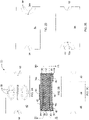
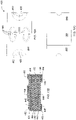
- FIGS. 2A, 2B, 2C, 2D, and 2E illustrate a conductive polymer device 30, in accordance with a first embodiment which is not part of the present invention.
- the device 30 includes a single active layer 32 of conductive polymer material, laminated between an upper metal foil electrode 34 and a lower foil electrode 36.
- First and second pluralities of through-hole via locations are defined in the sheet structure 10 ( FIG. 1A ). Each via location in the first plurality is separated from a corresponding via location in the second plurality by a pre-defined distance that corresponds to the length of a single device 30.
- An arcuate area of the upper electrode 34 adjacent each of the first via locations is removed (e.g., by conventional photo-resist masking and etching) to create an upper isolation area 38 at a first end of the upper electrode 34.
- an arcuate area of the lower electrode 36 adjacent each of the second via locations is removed to create a lower isolation area 40 at the opposite end of the second electrode 36.
- An upper insulation layer 42 which may be of prepreg, an insulative polymer, or an epoxy, is applied to the exposed surface of the upper electrode 34, and a lower insulation layer 44, of similar material, is applied to the exposed surface of the lower electrode 36.
- the upper insulation layer 42 fills the upper isolation area 38, while the lower insulation layer 44 fills the lower isolation area 40.
- a bottom metallization layer preferably a metal foil, (such as, for example, a copper foil) is applied to the exposed surface of the lower insulation layer.
- First and second surface mount terminals 46, 48 will be formed from the bottom metallization layer, as will be described below.
- a top metallization layer preferably a metal foil (such as, for example, a copper foil), may optionally be applied to the upper insulation layer 42 to form identification indicia 50, as also described below.
- the top metallization layer (if present) and the upper insulation layer 42 may be pre-formed and applied as a laminate, or they may be applied separately in sequence.
- the bottom metallization layer and the bottom insulation layer 44 may be applied either together as a pre-formed laminate, or separately in sequence.
- the result is a laminated structure comprising a single active polymer layer 32, an upper electrode 34, a lower electrode 36, a top insulation layer 42, a bottom insulation layer 44, a bottom metallization layer, and (optionally) a top metallization layer.
- a first through-hole via 52 is formed through the entire thickness of the above-described laminated structure (e.g. by mechanical or laser drilling) at each of the first plurality of via locations, and a second through-hole via 54 is similarly (and, preferably, simultaneously) formed through the entire thickness of the laminated structure at each of the second plurality of via locations.
- each device 30 has a first through-hole via 52 at a first end, and a second through-hole via 54 at the opposite end.
- the top and bottom surfaces of the structure and the inside surfaces of the through-hole vias 52, 54 are plated with one or more layers of conductive metal, thereby forming a first set of electrically conductive interconnections or "cross-conductors" 56 within each of the first set of vias 52, and a second set of cross-conductors 58 within each of the second set of vias 54.
- the metallization may be by any suitable process, and in a preferred embodiment, comprises at least an electroplated copper layer.
- Each of the first set of cross-conductors 56 establishes physical and electrical contact with the lower electrode 36, and the bottom metallization layer, and, if present, the top metallization layer, while being electrically isolated from the upper electrode 34 by the upper isolation area 38.
- each of the second set of cross-conductors 58 establishes physical and electrical contact with the upper electrode 34 and the top and bottom metallization layers, while being electrically isolated from the lower electrode 36 by the lower isolation area 40.
- the bottom metallization layer is formed into first and second planar surface-mount terminals 46, 48 by removing the central portion of the bottom metallization layer by any conventional technique, preferably by photo-resist masking and etching. This process leaves a planar metallized first surface-mount terminal 46 and a planar metallized second surface-mount terminal 48 on the bottom surface of the device 30, separated from each other by an exposed portion of the lower insulation layer 44.
- the first terminal 46 is in electrical contact with the lower electrode 36 through the first cross-conductor 56, while the second terminal 48 is in electrical contact with the upper electrode 34 through the second cross-conductor 58.
- the photo-resist masking and etching process may be employed to remove all of the top metallization layer except for those portions that represent the indicia 50.
- the exposed metal areas particularly the terminals 46, 48 and the cross-conductors 56, 58 (and the indicia 50, if present), may advantageously be over-plated with one or more solderable metal layers, such as, for example, electroless-plated nickel followed by immersion-plated gold (a process known as Electroless Nickel/Immersion Gold plating, or "ENIG" plating).
- a single electroless-plated layer of tin may be applied.
- the over-plating with solderable metals may be performed immediately after the copper-plating, and before the formation of the surface-mount terminals (and the optional indicia).
- the over-plating is preferably electroplated nickel followed by electroplated gold or tin.
- only an electroplated layer of tin may be applied.
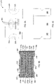
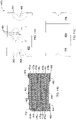
- FIGS. 3A, 3B, and 3C illustrate a multiple active layer device 70 which is not part of the invention and that is a variant of the embodiment of FIGS. 2A-2E , wherein the multiple active layer device 70 comprises at least a first active layer 72a and a second active layer 72b, of conductive polymer material, connected in parallel, and arranged in a vertically-stacked configuration with a single pair of surface-mount terminals.
- the first active layer 72a is laminated between first and second metal foil electrodes 74a, 74b in a first laminated sheet structure
- the second active layer 72b is laminated between third and fourth metal foil electrodes 74c, 74d in a second laminated sheet structure, each of the sheet structures being of the type described above and shown in FIGS.
- the first and second pluralities of via locations are defined as described above.
- An arcuate area of the first and fourth electrodes 74a, 74d adjacent each of the first via locations is removed (e.g., by conventional photo-resist masking and etching) to create an upper isolation area 76a and a lower isolation area 76b at a first end of the first and fourth electrodes 74a, 74d.
- an arcuate area of the second and third electrodes 74b, 74c adjacent each of the second via locations is removed to create intermediate isolation areas 78a, 78b at the opposite ends of the second and third electrodes 74c, 74d.
- the first and second laminated sheet structures are then laminated together into a multiple active layer laminated structure by an intermediate insulative layer 80 (prepreg, polymer, or epoxy), so that the upper and lower isolation areas 76a, 76b are aligned at a first end of the structure, and the intermediate isolation areas 78a, 78b are aligned at the opposite end of the structure.
- the intermediate isolation areas 78a, 78b are filled by the intermediate insulative layer 80.
- the second and third electrodes 74b, 74c may be soldered together, without the use of the intermediate insulative layer 80. Insulative material would then be screen printed so as to fill in the intermediate isolation areas 78a, 78b. The soldering of the electrodes together could lead to improved conduction of heat out of the active elements, resulting in faster electrical response to increases and decreases in device temperature.
- a top insulation layer 82 which may be of prepreg, an insulative polymer, or an epoxy, is applied to the exposed surface of the first electrode 74a, and a bottom insulation layer 84, of similar material, is applied to the exposed surface of the fourth electrode 74d.
- the top insulation layer 82 fills the upper isolation area 76a, while the bottom insulation layer 84 fills the lower isolation area 76b.
- a bottom metallization layer preferably a copper foil, is applied to the exposed surface of the bottom insulation layer to form first and second surface mount terminals or terminal pads 86, 88, as will be described below.
- a top metallization layer preferably a copper foil, may optionally be applied to the top insulation layer 82 to form identification indicia 90, as also described below.
- the top metallization layer (if present) and the top insulation layer 82 may be pre-formed and applied as a laminate, or they may be applied separately in sequence.
- the bottom metallization layer and the bottom insulation layer 84 may be applied either together as a pre-formed laminate, or separately in sequence.
- the result is a multiple active layer laminated structure comprising first and second active polymer layers 72a, 72b, a first or upper electrode 74a, intermediate second and third electrodes 74b, 74c, a fourth or lower electrode 74d, an intermediate insulation layer 80, a top insulation layer 82, a bottom insulation layer 84, a bottom metallization layer, and (optionally) a top metallization layer.
- a first through-hole via 92 is formed through the entire thickness of the above-described multiple active layer laminated structure (e.g. by mechanical or laser drilling) at each of the first plurality of via locations, and a second through-hole via 94 is similarly (and, preferably, simultaneously) formed through the entire thickness of the structure at each of the second plurality of via locations.
- each device 70 has a first through-hole via 92 at a first end, and a second through-hole via 94 at the opposite end.
- the top and bottom surfaces of the structure and the inside surfaces of the through-hole vias 92, 94 are plated with one or more layers of conductive metal, preferably copper, thereby forming a first set of cross-conductors 96 within each of the first set of vias 92, and a second set of cross-conductors 98 within each of the second set of vias 94.
- Each of the first set of cross-conductors 96 establishes physical and electrical contact with the second and third (intermediate) electrodes 74b, 74c and the top and bottom metallization layers, while being electrically isolated from the first (upper) electrode 74a by the upper isolation area 76a, and from the fourth (lower) electrode by the lower isolation layer 76b.
- each of the second set of cross-conductors 98 establishes physical and electrical contact with the first (upper) electrode 74a and the fourth (lower) electrode 74d and the top and bottom metallization layers, while being electrically isolated from the second and third (intermediate) electrodes 74b, 74c by the intermediate isolation areas 78a, 78b.
- the bottom metallization layer is formed into first and second terminals or terminal pads 86, 88 by removing the central portion of the bottom metallization layer by any conventional technique, preferably by photo-resist masking and etching. This process leaves a planar metallized first surface-mount terminal 86 and a planar metallized second surface-mount terminal 88 on the bottom surface device 70, separated from each other by an exposed portion of the bottom insulation layer 84.
- the first terminal 86 is in electrical contact with the second and third (intermediate) electrodes 74b, 74c through the first cross-conductor 96, while the second terminal 88 is in electrical contact with the first (upper) electrode 74a and the fourth (lower) electrode 74d through the second cross-conductor 98.
- the masking and photo-etching process may be employed to remove all of the top metallization layer except for those portions that represent the indicia 90.
- the exposed metal areas particularly the terminals 86, 88 and the cross-conductors 96, 98 (and the optional indicia 90, if present), may advantageously be over-plated with one or more solderable metal layers, such as, for example, nickel and gold ENIG plating, or just electroless tin plating.
- the overplating can be performed immediately after the copper plating with electroplated nickel followed by electroplated gold or tin, or just electroplated tin.
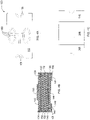
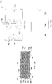
- FIGS. 4A, 4B, and 4C illustrate a conductive polymer device 130, in accordance with a second embodiment which is not part of the invention.
- the device 130 includes a single active layer 132 of conductive polymer material, laminated between an upper metal foil electrode 134 and a lower foil electrode 136.
- the device 130 is similar to the device 30, described above and illustrated in FIGS. 2A through, 2E , except that the upper electrode 134 is formed (by photo-resist masking and etching) with an upper isolation area 138 in the form of a narrow lateral band or strip that is spaced from a first end of the device 130 by a narrow upper residual foil area 139.
- the lower electrode 136 is likewise formed with a lower isolation area 140 in the form of a narrow lateral band or strip that is spaced from the second end of the device 130 by a narrow lower residual foil area 141.
- a top insulation layer 142 is applied or formed over the upper electrode 134 and the upper residual foil area 139, filling in the upper isolation area 138.
- a bottom insulation layer 144 is applied or formed over the lower electrode 136 and the lower residual foil area 141, filling in the lower isolation area 140.
- a bottom metallization layer preferably a copper foil, is applied to the exposed surface of the bottom insulation layer 144 to form first and second surface mount terminals or terminal pads 146, 148, as will be described below.
- a top metallization layer preferably a copper foil, may optionally be applied to the top insulation layer 142 to form identification indicia 150, as also described below.
- the top metallization layer (if present) and the top insulation layer 142 may be pre-formed and applied as a laminate, or they may be applied separately in sequence.
- the bottom metallization layer and the bottom insulation layer 144 may be applied either together as a pre-formed laminate, or separately in sequence. In either case, the result is a laminated structure comprising a single active polymer layer 132, an upper electrode 134, a lower electrode 136, a top insulation layer 142, a bottom insulation layer 144, a bottom metallization layer, and (optionally) a top metallization layer.
- the first and second pluralities of via locations are defined as described above.
- a first through-hole via 152 is formed through the entire thickness of the above-described laminated structure (e.g. by mechanical or laser drilling) at each of the first plurality of via locations, and a second through-hole via 154 is similarly (and, preferably, simultaneously) formed through the entire thickness of the multi-layer structure at each of the second plurality of via locations.
- each device 130 has a first through-hole via 152 at a first end, and a second through-hole via 154 at the opposite end.
- the top and bottom surfaces of the structure and the inside surfaces of the through-hole vias 152, 154 are plated with one or more layers of conductive metal, preferably copper ,thereby forming a first set of cross-conductors 156 within each of the first set of vias 152, and a second set of cross-conductors 158 within each of the second set of vias 154.
- Each of the first set of cross-conductors 156 establishes physical and electrical contact with the lower electrode 136 and the top and bottom metallization layers, while being electrically isolated from the upper electrode 134 by the upper isolation area 138.
- each of the second set of cross-conductors 158 establishes physical and electrical contact with the upper electrode 134 and the top and bottom metallization layers, while being electrically isolated from the lower electrode 136 by the lower isolation area 140.
- the bottom metallization layer is formed into first and second terminals 146, 148 by removing the central portion of the bottom metallization layer by any conventional technique, preferably by photo-masking and etching. This process leaves a planar metallized first surface-mount terminal 146 and a planar metallized second surface-mount terminal 148 on the bottom surface device 130, separated from each other by an exposed portion of the bottom insulation layer 144.
- the first terminal 146 is in electrical contact with the lower electrode 136 through the first cross-conductor 156, while the second terminal 148 is in electrical contact with the upper electrode 134 through the second cross-conductor 158.
- the masking and etching process may be employed to remove all of the top metallization layer except for those portions that represent the indicia 150.
- the exposed metal areas particularly the terminals 146, 148 and the cross-conductors 156, 158, may advantageously be over-plated with one or more solderable metal layers, such as, for example, the nickel and gold ENIG plating, as described above, or just electroless-plated tin.
- the over-plating can be electroplated nickel and gold, electroplated nickel and tin, or just electroplated tin, performed immediately after the copper plating step.
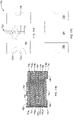
- FIGS. 5A, 5B, and 5C illustrate a multiple active layer device 170 which is not part of the invention and that is a variant of the embodiment of FIGS. 4A-4C , wherein the multiple active layer device 170 comprises at least a first active layer 172a and a second active layer 172b, of conductive polymer material, connected in parallel, and arranged in a vertically-stacked configuration with a single pair of surface-mount terminals.
- the first active layer 172a is laminated between first and second metal foil electrodes 174a, 174b in a first laminated sheet structure, and the second active layer 172b is laminated between third and fourth metal foil electrodes 174c, 174d in a second laminated sheet structure, each of the sheet structures being of the type described above and shown in FIGS. 1A and IB.
- the first and second pluralities of via locations are defined as described above.
- the first or upper electrode 174a is formed (by photo-resist masking and etching) with an upper isolation area 176a in the form of a narrow lateral band or strip that is spaced from a first end of the device 170 by a narrow upper residual foil area 177a.
- the fourth or lower electrode 174d is likewise formed with a lower isolation area 176b in the form of a narrow lateral band or strip that is spaced from the first end of the device 170 by a narrow lower residual foil area 177b.
- the second and third (intermediate) electrodes 174b, 174c are similarly formed with intermediate isolation areas 178a, 178b in the form of lateral bands or strips that are spaced from the second end of the device 170 by narrow intermediate residual foil areas 181a, 181b.
- the first and second laminated sheet structures are then laminated together into a multiple active layer laminated structure by an intermediate insulative layer 180 (prepreg, polymer, or epoxy), so that the upper and lower isolation areas 176a, 176b are aligned at a first end of the structure, and the intermediate isolation areas 178a, 178b are aligned at the opposite end of the structure.
- the intermediate isolation areas 178a, 178b are filled by the intermediate insulative layer 180.
- a top insulation layer 182 which may be of prepreg, an insulative polymer, or an epoxy, is applied to the exposed surfaces of the first electrode 174a and the upper residual foil area 177a, and a bottom insulation layer 184, of similar material, is applied to the exposed surfaces of the fourth electrode 174d and the lower residual foil area 177b.
- the top insulation layer 182 fills the upper isolation area 176a, while the bottom insulation layer 184 fills the lower isolation area 176b.
- a bottom metallization layer preferably a copper foil, is applied to the exposed surface of the bottom insulation layer to form first and second surface mount terminals 186, 188, as will be described below.
- a top metallization layer preferably a copper foil, may optionally be applied to the top insulation layer 182 to form identification indicia 190, as also described below.
- the top metallization layer (if present) and the top insulation layer 182 may be pre-formed and applied as a laminate, or they may be applied separately in sequence.
- the bottom metallization layer and the bottom insulation layer 184 may be applied either together as a pre-formed laminate, or separately in sequence.
- the result is a multiple active layer laminated structure comprising first and second active polymer layers 172a, 172b, a first or upper electrode 174a, intermediate second and third electrodes 174b, 174c, a fourth or lower electrode 174d, an intermediate insulation layer 180, a top insulation layer 182, a bottom insulation layer 184, a bottom metallization layer, and (optionally) a top metallization layer.
- a first through-hole via 192 is formed through the entire thickness of the above-described multiple active layer laminated structure (e.g. by mechanical or laser drilling) at each of the first plurality of via locations, and a second through-hole via 194 is similarly (and, preferably, simultaneously) formed through the entire thickness of the structure at each of the second plurality of via locations.
- each device 170 has a first through-hole via 192 at a first end, and a second through-hole via 194 at the opposite end.
- the top and bottom surfaces of the structure and the inside surfaces of the through-hole vias 192, 194 are plated with one or more layers of conductive metal, preferably copper, thereby forming a first set of cross-conductors 196 within each of the first set of vias 192, and a second set of cross-conductors 198 within each of the second set of vias 194.
- Each of the first set of cross-conductors 196 establishes physical and electrical contact with the second and third (intermediate) electrodes 174b, 174c and the top and bottom metallization layers, while being electrically isolated from the first (upper) electrode 174a by the upper isolation area 176a, and from the fourth (lower) electrode by the lower isolation layer 176b.
- each of the second set of cross-conductors 198 establishes physical and electrical contact with the first (upper) electrode 174a and the fourth (lower) electrode 174d and the top and bottom metallization layers, while being electrically isolated from the second and third (intermediate) electrodes 174b, 174c by the intermediate isolation areas 178a, 178b.
- the bottom metallization layer is formed into first and second terminals 186, 188 by removing the central portion of the bottom metallization layer by any conventional technique, preferably by photo-resist masking and etching. This process leaves a planar metallized first surface-mount terminal 186 and a planar metallized second surface-mount terminal 188 on the bottom surface of the device 170, separated from each other by an exposed portion of the bottom insulation layer 184.
- the first terminal 186 is in electrical contact with the second and third (intermediate) electrodes 174b, 174c through the first cross-conductor 196, while the second terminal 188 is in electrical contact with the first (upper) electrode 174a and the fourth (lower) electrode 174d through the second cross-conductor 198.
- the masking and photo-etching process may be employed to remove all of the top metallization layer except for those portions that represent the indicia 190.
- the exposed metal areas, particularly the terminals 186, 188 and the cross-conductors 196, 198, (and the indicia 190, if present) may advantageously be over-plated with one or more solderable metal layers, such as, for example, the nickel and gold ENIG plating, or just electroless-plated tin, as described above.
- the over-plating may electroplated nickel and hold, electroplated nickel and tin, or just electroplated tin, performed immediately after the copper plating step.
- FIGS. 6A, 6B, and 6C illustrate a conductive polymer device 230, in accordance with a third embodiment which is not part of the present invention.
- the device 230 includes a single active layer 232 of conductive polymer material, laminated between an upper metal foil electrode 234 and a lower foil electrode 236.
- This embodiment differs from the first embodiment described above and illustrated in FIGS. 2A-2C principally in that the vias in the laminated sheet structures are formed with a funnel-shaped upper opening, yielding a chamfered upper entry surface for the cross-conductors at each end of the device, as explained below.
- the device 230 includes an arcuate upper isolation area 238 between the upper electrode 234 and a first end of the device 230, adjacent a first through-hole via 252.
- the device also includes an arcuate lower isolation area 240 between the lower electrode 236 and the opposite end of the device 230, adjacent a second through-hole via 254.
- a top insulation layer 242 is formed or applied on the exposed surface of the upper electrode 234, filling in the upper isolation area 238, and a bottom insulation layer 244 is similarly formed or applied on the exposed surface of the lower electrode 236, filling in the lower isolation area 240.
- a bottom metallization layer preferably a copper foil
- a top metallization layer preferably a copper foil
- the top metallization layer (if present) and the top insulation layer 242 may be pre-formed and applied as a laminate, or they may be applied separately in sequence.
- the bottom metallization layer and the bottom insulation layer 234 may be applied either together as a pre-formed laminate, or separately in sequence.
- the result is a laminated structure comprising a single active polymer layer 232, an upper electrode 234, a lower electrode 236, a top insulation layer 242, a bottom insulation layer 244, a bottom metallization layer, and (optionally) a top metallization layer.
- a first through-hole via 252 is formed through the entire thickness of the above-described laminated structure (e.g. by mechanical or laser drilling) at each of the first plurality of via locations, and a second through-hole via 254 is similarly (and, preferably, simultaneously) formed through the entire thickness of the laminated structure at each of the second plurality of via locations.
- each device 230 has a first through-hole via 252 at a first end, and a second through-hole via 254 at the opposite end.
- each of the vias 252, 254 is chamfered or beveled by any suitable method or mechanism known in the art, such as, for example, a drill with a conical drill bit (not shown), to form a chamfered or beveled first entry hole 260 for the first via 252, and a similar chamfered or beveled second entry hole 262 for the second via 254.
- the first entry hole 260 extends through the upper insulation layer 242 and the first isolation area 238, leaving a portion of the first isolation area 238 to separate the first entry hole 260 from a first end of the upper electrode 234, while the second entry hole 262 extends through the upper insulation layer 242 to the second via 254 either adjacent to or through the opposite end of the upper electrode 234.
- the vias 252, 254 it is preferred to drill the vias 252, 254 first, and then to form the chamfered or beveled entry holes 260, 262, the chamfered or beveled entry holes 260, 262 may be formed at the pre-defined via locations before the vias 252, 254 are drilled.
- top and bottom surfaces of the structure and the inside surfaces of the through-hole vias 252, 254, including their respective entry holes 260, 262, are plated with one or more layers of conductive metal, preferably copper, thereby forming a first set of cross-conductors 256 within each of the first set of vias 252 and first chamfered or beveled entry hole 260, and a second set of cross-conductors 258 within each of the second set of vias 254 and second chamfered or beveled entry hole 262.
- Each of the first set of cross-conductors 256 establishes physical and electrical contact with the lower electrode 236 and the top and bottom metallization layers, while being electrically isolated from the upper electrode 234 by the upper isolation area 238.
- each of the second set of cross-conductors 258 establishes physical and electrical contact with the upper electrode 234 and the top and bottom metallization layers, while being electrically isolated from the lower electrode 236 by the lower isolation area 240.
- Each of the copper-plated first vias 252 provides a first cross-conductor 256 with a sloped shoulder provided by a first chamfered entry hole 260.
- each of the copper-plated second vias 254 provides a second cross-conductor 258 with a sloped shoulder provided by a second chamfered entry hole 262.
- the sloped shoulders of the cross-conductors 256, 258 establish a more intimate and secure contact with the top insulation layer 242 than that established by a cross-conductor formed through a straight via, such as that shown in FIGS. 2A-2C , for example
- the bottom metallization layer is formed into first and second terminals 246, 248 by removing the central portion of the bottom metallization layer by any conventional technique, preferably by photo-resist masking and etching. This process leaves a planar metallized first surface-mount terminal 246 and a planar metallized second surface-mount terminal 248 on the bottom surface device 230, separated from each other by an exposed portion of the bottom insulation layer 234.
- the first terminal 246 is in electrical contact with the lower electrode 236 through the first cross-conductor 256, while the second terminal 248 is in electrical contact with the upper electrode 234 through the second cross-conductor 258.
- the photo-resist masking and etching process may be employed to remove the entire top metallization layer except for those portions that represent the indicia 250.
- the exposed metal areas, particularly the terminals 246, 248 and the cross-conductors 256, 258 (and the indicia 250, if present) may advantageously be over-plated with one or more solderable metal layers, such as, for example, the nickel and gold ENIG plating, described above, or just electroless-plated tin.
- the over-plating may be electroplated nickel and gold, electroplated nickel and tin, or just electroplated tin, performed immediately after the copper plating step.
- FIGS. 7A, 7B, and 7C illustrate a multiple active layer device 270 which is not part of the invention and that is a variant of the third embodiment of FIGS. 6A-6C , wherein the multiple active layer device 270 comprises at least a first active layer 272a and a second active layer 272b, of conductive polymer material, connected in parallel, and arranged in a vertically-stacked configuration with only a single pair of surface-mount terminals.
- the first active layer 272a is laminated between first and second metal foil electrodes 274a, 274b in a first laminated sheet structure, and the second active layer 276b is laminated between fifth and fourth metal foil electrodes 274c, 274d in a second laminated sheet structure, each of the sheet structures being of the type described above and shown in FIGS. 1A and IB.
- the first and second pluralities of via locations are defined as described above.
- the first or upper electrode 274a is formed (by photo-resist masking and etching) with an arcuate upper isolation area 276a between the first electrode 274a and a first end of the device 270, adjacent to a first through-hole via 292.
- the fourth or lower electrode 274d is likewise formed with an arcuate lower isolation area 276b between the fourth electrode 274d and the first end of the device 270, adjacent to the first through-hole via 292.
- the second and third (intermediate) electrodes 274b, 274c are similarly formed with intermediate arcuate isolation areas 278a, 278b between the intermediate electrodes 274b, 274c and the second end of the device 270, adjacent to the second through-hole via 294.
- the first and second laminated sheet structures are then laminated together into a multiple active layer laminated structure by an intermediate insulative layer 280 (prepreg, polymer, or epoxy), so that the upper and lower isolation areas 276a, 276b are aligned at a first end of the structure, and the intermediate isolation areas 278a, 278b are aligned at the opposite end of the structure.
- the intermediate isolation areas 278a, 278b are filled by the intermediate insulative layer 280.
- a top insulation layer 282 which may be of prepreg, an insulative polymer, or an epoxy, is applied to the exposed surface of the first electrode 274a, and a bottom insulation layer 284, of similar material, is applied to the exposed surface of the fourth electrode 274d.
- the top insulation layer 282 fills the upper isolation area 276a, while the bottom insulation layer 284 fills the lower isolation area 276b.
- a bottom metallization layer preferably a copper foil, is applied to the exposed surface of the bottom insulation layer to form first and second surface mount terminals 286, 288, as will be described below.
- a top metallization layer preferably a copper foil, may optionally be applied to the top insulation layer 282 to form identification indicia 290, as also described below.
- the top metallization layer (if present) and the top insulation layer 282 may be pre-formed and applied as a laminate, or they may be applied separately in sequence.
- the bottom metallization layer and the bottom insulation layer 284 may be applied either together as a pre-formed laminate, or separately in sequence.
- the lamination of the first and second laminated sheet structures together with the intermediate insulative layer 280 may be performed simultaneously with one or more of the top insulating layer 282 and the top metallization layer and the bottom insulation layer 284 and the bottom metallization layer.
- the result is a multiple active layer laminated structure comprising first and second active polymer layers 272a, 272b, a first or upper electrode 274a, intermediate second and third electrodes 274b, 274c, a fourth or lower electrode 274d, an intermediate insulation layer 280, a top insulation layer 282, a bottom insulation layer 284, a bottom metallization layer, and (optionally) a top metallization layer.
- a first through-hole via 292 is formed through the entire thickness of the above-described multiple active layer laminated structure (e.g. by mechanical or laser drilling) at each of the first plurality of via locations, and a second through-hole via 294 is similarly (and, preferably, simultaneously) formed through the entire thickness of the structure at each of the second plurality of via locations.
- each device 270 has a first through-hole via 292 at a first end, and a second through-hole via 294 at the opposite end.
- each of the vias 292, 294 is chamfered by a drill using a conical drill bit (not shown) to form a chamfered or beveled first entry hole 300 for the first via 292, and a similar chamfered or beveled second entry hole 302 for the second via 294.
- the removal of the insulating material at the openings or entries of the vias 292, 294 may be accomplished by any suitable mechanical or chemical mechanism or process that may suggest itself to those skilled in the pertinent arts.
- the first entry hole 300 extends through the upper insulation layer 282 and the first isolation area 276a, leaving a portion of the first isolation area 276a to separate the first entry hole 300 from a first end of the upper electrode 274a, while the second entry hole 302 extends through the upper insulation layer 282 to the second via 294 adjacent to or through the opposite end of the first or upper electrode 274a.
- the entry holes 300, 302 may be formed at the pre-defined via locations before the vias 292, 294 are drilled.
- top and bottom surfaces of the structure and the inside surfaces of the through-hole vias 292, 294 and the chamfered entry holes 300, 302 are plated with one or more layers of conductive metal, preferably copper, thereby forming a first set of cross-conductors 296 within each of the first set of vias 292, and a second set of cross-conductors 298 within each of the second set of vias 294.
- Each of the first set of cross-conductors 296 establishes physical and electrical contact with the second and third (intermediate) electrodes 274b, 274c and the top and bottom metallization layers, while being electrically isolated from the first (upper) electrode 274a by the upper isolation area 276a, and from the fourth (lower) electrode 274d by the lower isolation layer 276b.
- each of the second set of cross-conductors 298 establishes physical and electrical contact with the first (upper) electrode 274a and the fourth (lower) electrode 274d and the top and bottom metallization layers, while being electrically isolated from the second and third (intermediate) electrodes 274b, 274c by the intermediate isolation areas 278a, 278b.
- Each of the copper-plated first vias 292 provides a first cross-conductor 296 with a sloped shoulder provided by a first chamfered entry hole 300.
- each of the copper-plated second vias 294 provides a second cross-conductor 298 with a sloped shoulder provided by a second chamfered entry hole 302.
- the sloped shoulders of the cross-conductors 296, 298 establish a more intimate and secure contact with the top insulation layer 282 than that established by a cross-conductor formed through a straight via, such as that shown in FIGS. 3A-3C , for example.
- the bottom metallization layer is formed into first and second terminals 286, 288 by removing the central portion of the bottom metallization layer by any conventional technique, preferably by photo-resist masking and etching. This process leaves a planar metallized first surface-mount terminal 286 and a planar metallized second surface-mount terminal 288 on the bottom surface of the device 270, separated from each other by an exposed portion of the bottom insulation layer 284.
- the first terminal 286 is in electrical contact with the second and third (intermediate) electrodes 274b, 274c through the first cross-conductor 296, while the second terminal 288 is in electrical contact with the first (upper) electrode 274a and the fourth (lower) electrode 274d through the second cross-conductor 298.
- the masking and photo-etching process may be employed to remove the entire top metallization layer except for those portions that represent the indicia 290.
- the exposed metal areas particularly the terminals 286, 288 and the cross-conductors 296, 298 (and the indicia 290, if present), may advantageously be over-plated with one or more solderable metal layers, such as, for example, the nickel and gold ENIG plating, or just electroless-plated tin.
- the over-plating may be electroplated nickel and gold, electroplated nickel and tin, or just electroplated tin, applied immediately after the copper plating step.
- FIGS. 8A, 8B, and 8C illustrate a conductive polymer device 330, in accordance with a fourth embodiment which is part of the present invention.
- the device 330 includes a single active layer 332 of conductive polymer material, laminated between an upper metal foil electrode 334 and a lower foil electrode 336.
- First and second pluralities of through-hole via locations are defined in the sheet structure 10 ( Fig. 1A ). Each via location in the first plurality is separated from a corresponding via location in the second plurality by a pre-defined distance that corresponds to the length of a single device 330.
- An arcuate area of the upper electrode 334 adjacent each of the first via locations is removed (e.g., by conventional photo-resist masking and etching) to create an upper isolation area 338 at a first end of the upper electrode 334.
- an arcuate area of the lower electrode 336 adjacent each of the second via locations is removed to create a lower isolation area 340 at the opposite end of the second electrode 336.
- a top insulation layer 342 which may be of prepreg, an insulative polymer, or an epoxy, is applied to the exposed surface of the upper electrode 334, and a bottom insulation layer 344, of similar material, is applied to the exposed surface of the lower electrode 336.
- the top insulation layer 342 fills the upper isolation area 338, while the bottom insulation layer 344 fills the lower isolation area 340.
- a bottom metallization layer preferably a copper foil, is applied to the exposed surface of the bottom insulation layer to form first and second surface mount terminals 346, 348, as will be described below.
- a top metallization layer preferably a copper foil, is applied to the top insulation layer 342 to form first and second anchor pads 360, 362, and (optionally) identification indicia 350, as discussed below.
- the top metallization layer and the top insulation layer 342 may be pre-formed and applied as a laminate, or they may be applied separately in sequence.
- the bottom metallization layer and the bottom insulation layer 344 may be applied either together as a pre-formed laminate, or separately in sequence. In either case, the result is a laminated structure comprising a single active polymer layer 332, an upper electrode 334, a lower electrode 336, a top insulation layer 342, a bottom insulation layer 344, a bottom metallization layer, and a top metallization layer.
- a first through-hole via 352 is formed through the entire thickness of the above-described laminated structure (e.g. by mechanical or laser drilling) at each of the first plurality of via locations, and a second through-hole via 354 is similarly (and, preferably, simultaneously) formed through the entire thickness of the laminated structure at each of the second plurality of via locations.
- each device 330 has a first through-hole via 352 at a first end, and a second through-hole via 354 at the opposite end.
- top and bottom surfaces of the structure and the inside surfaces of the through-hole vias 352, 354 are plated with one or more layers of conductive metal, preferably copper, thereby forming a first set of cross-conductors 356 within each of the first set of vias 352, and a second set of cross-conductors 358 within each of the second set of vias 354.
- a photo-resist masking and etching process is employed to form one or both of the first and second anchor pads 360, 362 and the optional indicia 350 from the top metallization layer, and to form the planar terminals 346, 348, from the bottom metallization layer.
- the masking and etching process may be employed either before or after the vias 352, 354 are formed and plated.
- Each of the first set of cross-conductors 356 establishes physical and electrical contact with the lower electrode 336 and the first terminal 346, while being electrically isolated from the upper electrode 334 by the upper isolation area 338.
- Each of the first cross-conductors 356 also is physically connected to a first anchor pad 360, which serves, along with the first terminal 346, as an anchor point for the first cross-conductor 356.
- each of the second set of cross-conductors 358 establishes physical and electrical contact with the upper electrode 334 and the second terminal 348, while being electrically isolated from the lower electrode 336 by the lower isolation area 340.
- Each of the second cross-conductors 358 also is physically connected to a second anchor pad 362, which serves, along with the second terminal 348, as an anchor point for the second cross-conductor 358.
- the exposed metal areas, particularly the terminals 346, 348, the cross-conductors 356, 358, and, optionally, the anchor pads 360, 362, and the optional indicia 350 (if present) may advantageously be over-plated with one or more solderable metal layers, such as, for example, the nickel and gold ENIG plating, or just electroless-plated tin.
- the over-plating may be electroplated nickel and gold, electroplated nickel and tin, or just electroplated tin, applied immediately after the copper plating step.
- FIGS. 9A, 9B, and 9C illustrate a multiple active layer device 370 that is a variant of the embodiment of FIGS. 8A-8C , wherein the multiple active layer device 370 comprises at least a first active layer 372a and a second active layer 372b, of conductive polymer material, connected in parallel, and arranged in a vertically-stacked configuration using only a single pair of surface-mount terminals.
- the first active layer 372a is laminated between first and second metal foil electrodes 374a, 374b in a first laminated sheet structure
- the second active layer 372b is laminated between third and fourth metal foil electrodes 374c, 374d in a second laminated sheet structure, each of the sheet structures being of the type described above and shown in FIGS.
- the first and second pluralities of via locations are defined as described above.
- An arcuate area of the first and fourth electrode 374a, 374d adjacent each of the first via locations is removed (e.g., by conventional photo-resist masking and etching) to create an upper isolation area 376a and a lower isolation area 376b at a first end of the first and fourth electrodes 374a, 374d.
- an arcuate area of the second and third electrodes 374b, 374c adjacent each of the second via locations is removed to create intermediate isolation areas 378a, 378b at the opposite ends of the second and third electrodes 374b, 374c.
- the first and second laminated sheet structures are then laminated together into a multiple active layer laminated structure by an intermediate insulative layer 380 (prepreg, polymer, or epoxy), so that the upper and lower isolation areas 376a, 376b are aligned at a first end of the structure, and the intermediate isolation areas 378a, 378b are aligned at the opposite end of the structure.
- the intermediate isolation areas 378a, 378b are filled by the intermediate insulative layer 380.
- a top insulation layer 382 which may be of prepreg, an insulative polymer, or an epoxy, is applied to the exposed surface of the first electrode 374a, and a bottom insulation layer 384, of similar material, is applied to the exposed surface of the fourth electrode 374d.
- the top insulation layer 382 fills the upper isolation area 376a, while the bottom insulation layer 384 fills the lower isolation area 376b.
- a bottom metallization layer preferably a copper foil, is applied to the exposed surface of the bottom insulation layer to form first and second surface mount terminals 386, 388, as will be described below.
- a top metallization layer preferably a copper foil, is applied to the top insulation layer 382 to form first and second anchor pads 400, 402, and (optionally) identification indicia 390, as also described below.
- the top metallization layer and the top insulation layer 382 may be pre-formed and applied as a laminate, or they may be applied separately in sequence.
- the bottom metallization layer and the bottom insulation layer 384 may be applied either together as a pre-formed laminate, or separately in sequence.
- the result is a multiple active layer laminated structure comprising first and second active polymer layers 372a, 372b, a first or upper electrode 374a, intermediate second and third electrodes 374b, 374c, a fourth or lower electrode 374d, an intermediate insulation layer 380, a top insulation layer 382, a bottom insulation layer 384, a bottom metallization layer, and a top metallization layer.
- a first through-hole via 392 is formed through the entire thickness of the above-described multiple active layer laminated structure (e.g. by mechanical or laser drilling) at each of the first plurality of via locations, and a second through-hole via 394 is similarly (and, preferably, simultaneously) formed through the entire thickness of the structure at each of the second plurality of via locations.
- each device 370 has a first through-hole via 392 at a first end, and a second through-hole via 394 at the opposite end.
- top and bottom surfaces of the structure and the inside surfaces of the through-hole vias 392, 394 are plated with one or more layers of conductive metal, preferably copper, thereby forming a first set of cross-conductors 396 within each of the first set of vias 392, and a second set of cross-conductors 398 within each of the second set of vias 394.
- a photo-resist masking and etching process is employed to form one or both of the first and second anchor pads 400, 402 and the optional indicia 390 from the top metallization layer, and to form the planar terminals 386, 388, from the bottom metallization layer.
- Each of the first set of cross-conductors 396 establishes physical and electrical contact with the second and third (intermediate) electrodes 374b, 374c and the first terminal 386, while being electrically isolated from the first (upper) electrode 374a and from the fourth (lower) electrode 374d by the upper isolation area 376a and the lower isolation area 376b, respectively.
- Each of the first cross-conductors 396 also is physically connected to a first anchor pad 400, which serves, along with the first terminal 386, as an anchor point for the first cross-conductor 396.
- each of the second set of cross-conductors 398 establishes physical and electrical contact with the first (upper) electrode 374a, the fourth (lower) electrode 374d, and the second terminal 388, while being electrically isolated from the second and third (intermediate) electrodes 374b, 374c by the intermediate isolations area 378a, 378b.
- Each of the second cross-conductors 398 also is physically connected to a second anchor pad 402, which serves, along with the second terminal 388, as an anchor point for the second cross-conductor 398.
- the exposed metal areas may advantageously be over-plated with one or more solderable metal layers, such as nickel and gold ENIG plating or electroless tin plating.
- the over-plating may be electroplated nickel and gold, electroplated nickel and tin, or just electroplated tin, applied immediately after the copper plating step.
- FIGS. 10A, 10B, and 10C illustrate a conductive polymer device 430, in accordance with a fifth embodiment which is part of the present invention.
- the device 430 includes a single active layer 432 of conductive polymer material, laminated between an upper metal foil electrode 434 and a lower foil electrode 436.
- the device 430 includes an arcuate upper isolation area 438 between the upper electrode 434 and a first end of the device 430, adjacent a first through-hole via 452.
- the device also includes an arcuate lower isolation area 440 between the lower electrode 436 and the opposite end of the device 430, adjacent a second through-hole via 454.
- a top insulation layer 442 is formed or applied on the exposed surface of the upper electrode 434, filling in the upper isolation area 438, and a bottom insulation layer 444 is similarly formed or applied on the exposed surface of the lower electrode 436, filling in the lower isolation area 440.
- a bottom metallization layer 22 ( FIGS. 1A, 1B ), preferably a copper foil, is applied to the exposed surface of the bottom insulation layer to form first and second surface mount terminals 446, 448, as will be described below.
- a top metallization layer 24 ( FIGS. 1A and 1B ) preferably a copper foil, is applied to the top insulation layer 442 to form an anchor pad 460 and (optionally) identification indicia 450, as also described below.
- the top metallization layer 18 and the top insulation layer 442 may be pre-formed and applied as a laminate, or they may be applied separately in sequence.
- the bottom metallization layer 20 and the bottom insulation layer 444 may be applied either together as a pre-formed laminate, or separately in sequence. In either case, the result is a laminated structure comprising a single active polymer layer 432, an upper electrode 434, a lower electrode 436, a top insulation layer 442, a bottom insulation layer 444, a bottom metallization layer and a top metallization layer.
- a first through-hole via 452 is formed through the entire thickness of the above-described laminated structure (e.g. by mechanical or laser drilling) at each of the first plurality of via locations, and a second through-hole via 454 is similarly (and, preferably, simultaneously) formed through the entire thickness of the laminated structure at each of the second plurality of via locations.
- each device 430 has a first through-hole via 452 at a first end, and a second through-hole via 454 at the opposite end.
- the top entrance or opening of the second via 454 is chamfered or beveled by any suitable mechanism or process, such as, for example, a drill with a conical drill bit (not shown), to form a chamfered or beveled second entry hole 462 for the second via 454.
- the chamfered or beveled second entry hole 462 extends through the upper insulation layer 442 to the second via 454 adjacent to or through an end of the upper electrode 434.
- the chamfered entry hole 462 may be formed at the pre-defined second via locations before the vias 452, 454 are drilled.
- top and bottom surfaces of the structure and the inside surfaces of the through-hole vias 452, 454, including the chamfered entry hole 462, are plated with one or more layers of conductive metal, preferably copper, thereby forming a first set of cross-conductors 456 within each of the first set of vias 452, and a second set of cross-conductors 458 within each of the second set of vias 454 and their associated chamfered second entry holes 462.
- a photo-resist masking and etching process is employed to form the anchor pad 460 and the optional indicia 450 from the top metallization layer, and to form one or both of the planar terminals 446, 448 from the bottom metallization layer.
- each of the first set of cross-conductors 456 establishes physical and electrical contact with the lower electrode 436 and the first terminal 446, while being electrically isolated from the upper electrode 434 by the upper isolation area 438.
- each of the second set of cross-conductors 458 establishes physical and electrical contact with the upper electrode 434 and the second terminal 448, while being electrically isolated from the lower electrode 436 by the lower isolation area 440.
- the first terminal 446 is in electrical contact with the lower electrode 436 through the first cross-conductor 456, while the second terminal 448 is in electrical contact with the upper electrode 434 through the second cross-conductor 458.
- the exposed metal areas may advantageously be over-plated with one or more solderable metal layers, such as, for example, nickel and gold ENIG plating, or electroless tin plating.
- the over-plating may be electroplated nickel and gold, electroplated nickel and tin, or just electroplated tin, applied immediately after the copper plating step.
- the upper and lower ends of the first cross-conductor 456 are respectively anchored by their connection to the anchor pad 460 and the first terminal 446.
- the upper and lower ends of the second cross-conductor 458 are respectively anchored by their connection to the upper electrode 434 and the second terminal 448.
- FIGS. 11A, 11B, and 11C illustrate a multiple active layer device 470 that is a variant of the embodiment of FIGS. 10A-10C , wherein the multiple active layer device 470 comprises at least a first active layer 472a and a second active layer 472b, of conductive polymer material, connected in parallel, and arranged in a vertically-stacked configuration, using only a single pair of surface-mount terminals.
- the first active layer 472a is laminated between first and second metal foil electrodes 474a, 474b in a first laminated sheet structure
- the second active layer 472b is laminated between third and fourth metal foil electrodes 474c, 474d in a second laminated sheet structure, each of the sheet structures being of the type described above and shown in FIGS.
- the first and second pluralities of via locations are defined as described above.
- the first or upper electrode 474a is formed (by photo-resist masking and etching) with an arcuate upper isolation area 476a between the first electrode 474a and a first end of the device 470, adjacent a first through-hole via 492.
- the fourth or lower electrode 474d is likewise formed with an arcuate lower isolation area 476b between the fourth electrode 476d and the first end of the device 470.
- the second and third (intermediate) electrodes 474b, 474c are similarly formed with intermediate arcuate isolation areas 478a, 478b between the intermediate electrodes 474b, 474c and the second end of the device 470.
- the first and second laminated sheet structures are then laminated together into a multiple active layer laminated structure by an intermediate insulative layer 480 (prepreg, polymer, or epoxy), so that the upper and lower isolation areas 476a, 476b are aligned at a first end of the structure, and the intermediate isolation areas 478a, 478b are aligned at the opposite end of the structure.
- the intermediate isolation areas 478a, 478b are filled by the intermediate insulative layer 480.
- a top insulation layer 482 which may be of prepreg, an insulative polymer, or an epoxy, is applied to the exposed surface of the first electrode 474a, and a bottom insulation layer 484, of similar material, is applied to the exposed surface of the fourth electrode 474d.
- the top insulation layer 482 fills the upper isolation area 476a, while the bottom insulation layer 484 fills the lower isolation area 476b.
- a bottom metallization layer preferably a copper foil, is applied to the exposed surface of the bottom insulation layer 484, and it is photo-resist masked and etched to form first and second surface mount terminals 486, 488 separated by an exposed area of the bottom insulation layer 484.
- a top metallization layer preferably a copper foil, is applied to the top insulation layer 482, and it is photo-resist masked and etched to form an anchor pad 500 and (optionally) identification indicia 490.
- the photo-resist masking and etching of the top and bottom metallization layers may be performed either before or after the vias 492, 494 are formed and plated, as described below.
- the top metallization layer and the top insulation layer 482 may be pre-formed and applied as a laminate, or they may be applied separately in sequence.
- the bottom metallization layer and the bottom insulation layer 484 may be applied either together as a pre-formed laminate, or separately in sequence.
- the result is a multiple active layer laminated structure comprising first and second active polymer layers 472a, 472b, a first or upper electrode 474a, intermediate second and third electrodes 474b, 474c, a fourth or lower electrode 474d, an intermediate insulation layer 480, a top insulation layer 482, a bottom insulation layer 484, a bottom metallization layer, and a top metallization layer.
- the top and bottom metallization layers may be formed into the anchor pad 500, the indicia 490, and the terminals 486, 488.
- a first through-hole via 492 is formed through the entire thickness of the above-described multiple active layer laminated structure (e.g. by mechanical or laser drilling) at each of the first plurality of via locations, and a second through-hole via 494 is similarly (and, preferably, simultaneously) formed through the entire thickness of the structure at each of the second plurality of via locations.
- each device 470 has a first through-hole via 492 at a first end, and a second through-hole via 494 at the opposite end.
- the top entrance or opening of the second via 494 is chamfered or beveled by any suitable mechanical or chemical means, such as, for example, a drill with a conical drill bit (not shown), to form a chamfered or beveled entry hole 502 for the second via 494.
- the chamfered or beveled entry hole 502 extends through the top insulation layer 482 to the second via 494, either adjacent to or through an end of the first or upper electrode 474a.
- the chamfered entry hole 502 may be formed at the pre-defined via locations before the second vias 492, 494 are drilled.
- top and bottom surfaces of the structure and the inside surfaces of the through-hole vias 492, 494, including the chamfered or beveled entry hole 502 of each of the second vias 494, are plated with one or more layers of conductive metal, preferably copper, thereby forming a first set of cross-conductors 496 within each of the first set of vias 492, and a second set of cross-conductors 498 within each of the second set of vias 494.
- a photo-resist masking and etching process is employed to form the anchor pad 500 and the optional indicia 490 from the top metallization layer, and to form the planar terminals 486, 488 from the bottom metallization layer.
- Each of the first set of cross-conductors 496 establishes physical and electrical contact with the second and third (intermediate) electrodes 474b, 474c, the anchor pad 500, and the first planar terminal 486, while being electrically isolated from the first (upper) electrode 474a by the upper isolation area 476a, and from the fourth (lower) electrode 474d by the lower isolation layer 476b.
- each of the second set of cross-conductors 498 establishes physical and electrical contact with the first (upper) electrode 474a, the fourth (lower) electrode 474d, and the second planar terminal 488, while being electrically isolated from the second and third (intermediate) electrodes 474b, 474c by the intermediate isolation areas 478a, 478b.
- the first terminal 486 is in electrical contact with the second and third (intermediate) electrodes 474b, 474c through the first cross-conductor 496, while the second terminal 488 is in electrical contact with the first (upper) electrode 474a and the fourth (lower) electrode 474d through the second cross-conductor 498.
- the upper and lower ends of the first cross-conductor 496 are respectively anchored by their connection to the anchor pad 500 and the first planar terminal 486.
- the upper and lower ends of the second cross-conductor 498 are respectively anchored by their connection to the upper electrode 474a and the lower second terminal 488.
- the exposed metal areas, particularly the terminals 486, 488, the cross-conductors 496, 498, and optionally the anchor pad 500 and the optional indicia 490 (if present) may advantageously be over-plated with one or more solderable metal layers, such as, for example, nickel and gold ENIG plating, or electroless tin plating.
- the over-plating may be electroplated nickel and gold, electroplated nickel and tin, or electroplated tin, applied immediately after the copper plating step.
- FIGS. 12A, 12B, and 12C illustrate a conductive polymer device 530.
- the device 530 includes a single active layer 532 of conductive polymer material, laminated between an upper metal foil electrode 534 and a lower foil electrode 536.
- This embodiment which is not part of the invention is similar to the embodiment of FIGS. 10A-10C , except that instead of a chamfered or beveled entry hole for the via at the end of the device opposite the anchor pad, there is provided a plated anchor element, as will be described below, by the removal of part of the top insulation layer.
- the device 530 includes an arcuate upper isolation area 538 between the upper electrode 534 and a first end of the device 530, adjacent a first through-hole via 552.
- the device 530 also includes an arcuate lower isolation area 540 between the lower electrode 536 and the opposite end of the device 530, adjacent a second through-hole via 554.
- a top insulation layer 542 is formed or applied on the exposed surface of the upper electrode 534, filling in the upper isolation area 538, and a bottom insulation layer 544 is similarly formed or applied on the exposed surface of the lower electrode 536, filling in the lower isolation area 540.
- a bottom metallization layer preferably a copper foil
- first and second surface mount terminals 546, 548 are applied to the exposed surface of the bottom insulation layer to form first and second surface mount terminals 546, 548, as will be described below.
- a top metallization layer preferably a copper foil
- the top metallization layer and the top insulation layer 542 may be pre-formed and applied as a laminate, or they may be applied separately in sequence.
- the bottom metallization layer and the bottom insulation layer 544 may be applied either together as a pre-formed laminate, or separately in sequence.
- the result is a laminated structure comprising a single active polymer layer 532, an upper electrode 534, a lower electrode 536, a top insulation layer 542, a bottom insulation layer 544, a bottom metallization layer, and a top metallization layer.
- a first through-hole via 552 is formed through the entire thickness of the above-described laminated structure (e.g. by mechanical or laser drilling) at each of the first plurality of via locations, and a second through-hole via 554 is similarly (and, preferably, simultaneously) formed through the entire thickness of the laminated structure at each of the second plurality of via locations.
- each device 530 has a first through-hole via 552 at a first end, and a second through-hole via 554 at the opposite end.
- An arcuate portion of the top insulation layer 542 adjacent the second via 554 is then removed by any suitable process, such as chemical etching, plasma etching, mechanical drilling or laser drilling, to form an exposed anchor surface 564 on the upper electrode 534, the purpose of which will be discussed below.
- the anchor surface 564 may be formed at the pre-defined second via locations before the vias 552, 554 are drilled.
- top and bottom surfaces of the structure and the inside surfaces of the through-hole vias 552, 554, as well as the anchor surface 564, are plated with one or more layers of conductive metal, preferably copper, thereby forming a first set of cross-conductors 556 within each of the first set of vias 552, a second set of cross-conductors 558 within each of the second set of vias 554, and a plated anchor element 562 on the anchor surface 564, wherein the plated anchor element 562 is contiguous with the second cross-conductor 558.
- a photo-resist masking and etching process is employed to form the anchor pad 560 adjacent the first through-hole via 552 (as well as the optional indicia 550) from the top metallization layer, and to form the planar terminals 546, 548 from the bottom metallization layer.
- the masking and etching process may be employed either before or after the vias 552, 554 are formed and plated.
- Each of the first set of cross-conductors 556 establishes physical and electrical contact with the lower electrode 536 and the first terminal 546, while being electrically isolated from the upper electrode 534 by the upper isolation area 538.
- each of the second set of cross-conductors 558 establishes physical and electrical contact with the upper electrode 534 and the second terminal 548, while being electrically isolated from the lower electrode 536 by the lower isolation area 540.
- the first terminal 546 is in electrical contact with the lower electrode 536 through the first cross-conductor 556
- the second terminal 548 is in electrical contact with the upper electrode 534 through the second cross-conductor 558.
- the exposed metal areas may advantageously be over-plated with one or more solderable metal layers, such as, for example, nickel and gold ENIG plating ore electroless tin plating.
- the over-plating may be electroplated nickel and gold, electroplated nickel and tin, or electroplated tin, applied immediately after the copper plating step.
- the upper and lower ends of the first cross-conductor 556 are respectively anchored by their connection to the anchor pad 560 and the first terminal 546.
- the upper end of the second cross-conductor 558 is anchored by its connection to the upper electrode 534 and to the anchor element 562, while the lower end of the second cross-conductor is anchored by its connection to the second terminal 548.
- the anchor element 562 provides a more intimate and secure connection and contact between the second cross-conductor 558 and the exposed anchor surface 564 on the upper electrode 534 than that established by a cross-conductor formed through a straight via, such as shown in FIGS. 3A-3C , for example. This enhances the structural integrity of the device without unduly restraining the thermal expansion of the polymeric active layer 532.
- FIGS. 13A, 13B, and 13C illustrate a multiple active layer device 570 which is not part of the invention and that is a variant of the embodiment of FIGS. 12A-12C , wherein the multiple active layer device 570 comprises at least a first active layer 572a and a second active layer 572b, of conductive polymer material, connected in parallel, and arranged in a vertically-stacked configuration with only a single pair of surface-mount terminals.
- the first active layer 572a is laminated between first and second metal foil electrodes 574a, 574b in a first laminated sheet structure, and the second active layer 572b is laminated between third and fourth metal foil electrodes 574c, 574d in a second laminated sheet structure, each of the sheet structures being of the type described above and shown in FIGS. 1A and IB.
- the first and second pluralities of via locations are defined as described above.
- the first or upper electrode 574a is formed (by photo-resist masking and etching) with an arcuate upper isolation area 576a between the first electrode 574a and a first end of the device 570, adjacent a first through-hole via 592.
- the fourth or lower electrode 574d is likewise formed with an arcuate lower isolation area 576b between the fourth electrode 574d and the first end of the device 570, adjacent the first through-hole via 592.
- the second and third (intermediate) electrodes 574b, 574c are similarly formed with intermediate arcuate isolation areas 578a, 578b between the intermediate electrodes 574b, 574c and the second end of the device 570, adjacent a second through-hole via 594.
- the first and second laminated sheet structures are then laminated together into a multiple active layer laminated structure by an intermediate insulative layer 580 (prepreg, polymer, or epoxy), so that the upper and lower isolation areas 576a, 576b are aligned at a first end of the structure, and the intermediate isolation areas 578a, 578b are aligned at the opposite end of the structure.
- the intermediate isolation areas 578a, 578b are filled by the intermediate insulative layer 580.
- a top insulation layer 582 which may be of prepreg, an insulative polymer, or an epoxy, is applied to the exposed surface of the first electrode 574a, and a bottom insulation layer 584, of similar material, is applied to the exposed surface of the fourth electrode 574d.
- the top insulation layer 582 fills the upper isolation area 576a, while the bottom insulation layer 584 fills the lower isolation area 576b.
- a bottom metallization layer preferably a copper foil, is applied to the exposed surface of the bottom insulation layer 584, and it is photo-resist masked and etched to form first and second surface mount terminals 586, 588 separated by an exposed area of the bottom insulation layer 584.
- a top metallization layer preferably a copper foil, is applied to the top insulation layer 582, and it is photo-resist masked and etched to form an anchor pad 600 and (optionally) identification indicia 590.
- the photo-resist masking and etching of the top and bottom metallization layers may be performed either before or after the vias 592, 594 are formed and plated, as described below.
- the top metallization layer and the top insulation layer 582 may be pre-formed and applied as a laminate, or they may be applied separately in sequence.
- the bottom metallization layer and the bottom insulation layer 584 may be applied either together as a pre-formed laminate, or separately in sequence.
- the result is a multiple active layer laminated structure comprising first and second active polymer layers 572a, 572b, a first or upper electrode 574a, intermediate second and third electrodes 574b, 574c, a fourth or lower electrode 574d, an intermediate insulation layer 580, a top insulation layer 582, a bottom insulation layer 584, a bottom metallization layer, and a top metallization layer.
- the top metallization layer is formed into the anchor pad 600 and the optional indicia 590
- the bottom metallization layer is formed into the planar terminals 586, 588, by any conventional process, such as photo-resist masking and etching, which may be performed either before or after the formation and plating of the vias, as described below.
- a first through-hole via 592 is formed through the entire thickness of the above-described multiple active layer laminated structure (e.g. by mechanical or laser drilling) at each of the first plurality of via locations, and a second through-hole via 594 is similarly (and, preferably, simultaneously) formed through the entire thickness of the structure at each of the second plurality of via locations.
- each device 570 has a first through-hole via 592 at a first end, and a second through-hole via 594 at the opposite end.
- An arcuate portion of the top insulation layer 582 adjacent the second via 594 is then removed by any suitable process, such as chemical etching, plasma etching, mechanical drilling or laser drilling, to form an exposed anchor surface 604 on the upper electrode 574a, the purpose of which will be discussed below.
- any suitable process such as chemical etching, plasma etching, mechanical drilling or laser drilling, to form an exposed anchor surface 604 on the upper electrode 574a, the purpose of which will be discussed below.
- the anchor surface 604 may be formed at the pre-defined second via locations before the vias 592, 594 are drilled.
- top and bottom surfaces of the structure and the inside surfaces of the through-hole vias 592, 594, as well as the anchor surface 604, are plated with one or more layers of conductive metal, preferably copper, thereby forming a first set of cross-conductors 596 within each of the first set of vias 592, a second set of cross-conductors 598 within each of the second set of vias 594, and a plated anchor element 602 on the anchor surface 604, wherein the plated anchor element 602 is contiguous with the second cross-conductor 598.
- a photo-resist masking and etching process is employed to form the anchor pad 600 adjacent the first through-hole via 592 (as well as the optional indicia 590) from the top metallization layer, and to form the planar terminal pads 586, 588 from the bottom metallization layer.
- the masking and etching process may be performed either before or after the vias 592, 594 are formed and plated.
- Each of the first set of cross-conductors 596 establishes physical and electrical contact with the second and third (intermediate) electrodes 574b, 574c, the anchor pad 600, and the first planar terminal 586, while being electrically isolated from the first (upper) electrode 574a by the upper isolation area 576a, and from the fourth (lower) electrode 574d by the lower isolation layer 576b.
- each of the second set of cross-conductors 598 establishes physical and electrical contact with the first (upper) electrode 574a, the fourth (lower) electrode 574d, and the second planar terminal 588, while being electrically isolated from the second and third (intermediate) electrodes 574b, 574c by the intermediate isolation areas 578a, 578b.
- the first terminal 586 is in electrical contact with the second and third (intermediate) electrodes 574b, 574c through the first cross-conductor 596, while the second terminal 588 is in electrical contact with the first (upper) electrode 574a and the fourth (lower) electrode 574d through the second cross-conductor 598.
- the upper and lower ends of the first cross-conductor 596 are respectively anchored by their connection to the anchor pad 600 and the first planar terminal 586.
- the upper end of the second cross-conductor 598 is anchored by its connection to the upper electrode 574a and to the anchor element 602, while the lower end of the second cross-conductor is anchored by its connection to the lower second terminal 588.
- the exposed metal areas, particularly the terminals 586, 588, the cross-conductors 596, 598, the anchor pad 600, and the plated anchor element 602 (and the indicia 590, if present), may advantageously be over-plated with one or more solderable metal layers, such as, for example, nickel and gold ENIG plating or electroless tin plating.
- the over-plating may be electroplated nickel and gold, electroplated nickel and tin, or electroplated tin, applied immediately after the copper plating step.
- FIGS. 14A, 14B, and 14C illustrate a conductive polymer device 630.
- the device 630 is not part of the invention and differs from the above-described embodiment of FIGS. 8A-8C in that it has only one anchor pad on a top insulation layer.
- the device 630 includes a single active layer 632 of conductive polymer material, laminated between an upper metal foil electrode 634 and a lower foil electrode 636.
- First and second pluralities of through-hole via locations are defined in the sheet structure 10 ( FIG. 1A ). Each via location in the first plurality is separated from a corresponding via location in the second plurality by a pre-defined distance that corresponds to the length of a single device 630.
- An arcuate area of the upper electrode 634 adjacent each of the first via locations is removed (e.g., by conventional photo-resist masking and etching) to create an upper isolation area 638 at a first end of the upper electrode 634.
- an arcuate area of the lower electrode 636 adjacent each of the second via locations is removed to create a lower isolation area 640 at the opposite end of the second electrode 636.
- a top insulation layer 642 which may be of prepreg, an insulative polymer, or an epoxy, is applied to the exposed surface of the upper electrode 634, and a bottom insulation layer 644, of similar material, is applied to the exposed surface of the lower electrode 636.
- the top insulation layer 642 fills the upper isolation area 638, while the bottom insulation layer 644 fills the lower isolation area 640.
- a bottom metallization layer preferably a copper foil, is applied to the exposed surface of the bottom insulation layer to form first and second surface mount terminals 646, 648, as will be described below.
- a top metallization layer preferably a copper foil, is applied to the top insulation layer 642 to form an anchor pad 660, and (optionally) identification indicia 650, as discussed below.
- the top metallization layer and the top insulation layer 642 may be pre-formed and applied as a laminate, or they may be applied separately in sequence.
- the bottom metallization layer and the bottom insulation layer 644 may be applied either together as a pre-formed laminate, or separately in sequence. In either case, the result is a laminated structure comprising a single active polymer layer 632, an upper electrode 634, a lower electrode 636, a top insulation layer 642, a bottom insulation layer 644, a bottom metallization layer, and a top metallization layer.
- a first through-hole via 652 is formed through the entire thickness of the above-described laminated structure (e.g. by mechanical or laser drilling) at each of the first plurality of via locations, and a second through-hole via 654 is similarly (and, preferably, simultaneously) formed through the entire thickness of the laminated structure at each of the second plurality of via locations.
- each device 630 has a first through-hole via 652 at a first end, and a second through-hole via 654 at the opposite end.
- top and bottom surfaces of the structure and the inside surfaces of the through-hole vias 652, 654 are plated with one or more layers of conductive metal, preferably copper, thereby forming a first set of cross-conductors 656 within each of the first set of vias 652, and a second set of cross-conductors 658 within each of the second set of vias 654.
- a photo-resist masking and etching process is employed to form anchor pad 660, and the optional indicia 650 from the top metallization layer, and to form the planar terminals 646, 648, from the bottom metallization layer.
- the masking and etching process may be employed either before or after the vias 652, 654 are formed and plated.
- Each of the first set of cross-conductors 656 establishes physical and electrical contact with the lower electrode 636 and the first terminal 646, while being electrically isolated from the upper electrode 634 by the upper isolation area 638.
- Each of the first cross-conductors 656 also is physically connected to a first anchor pad 660, which serves, along with the first terminal 646, as an anchor point for the first cross-conductor 656.
- each of the second set of cross-conductors 658 establishes physical and electrical contact with the upper electrode 634 and the second terminal 648, while being electrically isolated from the lower electrode 636 by the lower isolation area 640.
- the exposed metal areas may advantageously be over-plated with one or more solderable metal layers, such as, for example, nickel and gold ENIG plating or electroless tin plating.
- the over-plating may be electroplated nickel and gold, electroplated nickel and tin, or electroplated tin applied immediately after the copper plating step.
- FIGS. 15A, 15B, and 15C illustrate a multiple active layer device 670 which is not part of the invention and that is a variant of the embodiment of FIGS. 14A-14C , wherein the multiple active layer device 670 comprises at least a first active layer 672a and a second active layer 672b, of conductive polymer material, connected in parallel, and arranged in a vertically-stacked configuration with only a single pair of surface-mount terminals.
- the first active layer 672a is laminated between first and second metal foil electrodes 674a, 674b in a first laminated sheet structure, and the second active layer 672b is laminated between third and fourth metal foil electrodes 674c, 674d in a second laminated sheet structure, each of the sheet structures being of the type described above and shown in FIGS. 1A and IB.
- the first and second pluralities of via locations are defined as described above.
- An arcuate area of the first and fourth electrode 674a, 674d adjacent each of the first via locations is removed (e.g., by conventional photo-resist masking and etching) to create an upper isolation area 676a and a lower isolation area 676b at a first end of the first and fourth electrodes 674a, 674d.
- first and second laminated sheet structures are then laminated together into a multiple active layer laminated structure by an intermediate insulative layer 680 (prepreg, polymer, or epoxy), so that the upper and lower isolation areas 676a, 676b are aligned at a first end of the structure, and the intermediate isolation areas 678a, 678b are aligned at the opposite end of the structure.
- the intermediate isolation areas 678a, 678b are filled by the intermediate insulative layer 680.
- a top insulation layer 682 which may be of prepreg, an insulative polymer, or an epoxy, is applied to the exposed surface of the first electrode 674a, and a bottom insulation layer 684, of similar material, is applied to the exposed surface of the fourth electrode 674d.
- the top insulation layer 682 fills the upper isolation area 676a, while the bottom insulation layer 684 fills the lower isolation area 676b.
- a bottom metallization layer preferably a copper foil, is applied to the exposed surface of the bottom insulation layer to form first and second surface mount terminals 686, 688, as will be described below.
- a top metallization layer preferably a copper foil, is applied to the top insulation layer 682 to form an anchor pad 700 and (optionally) identification indicia 690, as also described below.
- the top metallization layer and the top insulation layer 682 may be pre-formed and applied as a laminate, or they may be applied separately in sequence.
- the bottom metallization layer and the bottom insulation layer 684 may be applied either together as a pre-formed laminate, or separately in sequence.
- the result is a multiple active layer laminated structure comprising first and second active polymer layers 672a, 672b, a first or upper electrode 674a, intermediate second and third electrodes 674b, 674c, a fourth or lower electrode 674d, an intermediate insulation layer 680, a top insulation layer 682, a bottom insulation layer 684, a bottom metallization layer, and a top metallization layer.
- a first through-hole via 692 is formed through the entire thickness of the above-described multiple active layer laminated structure (e.g. by mechanical or laser drilling) at each of the first plurality of via locations, and a second through-hole via 694 is similarly (and, preferably, simultaneously) formed through the entire thickness of the structure at each of the second plurality of via locations.
- each device 670 has a first through-hole via 692 at a first end, and a second through-hole via 694 at the opposite end.
- top and bottom surfaces of the structure and the inside surfaces of the through-hole vias 692, 694 are plated with one or more layers of conductive metal, preferably copper, thereby forming a first set of cross-conductors 696 within each of the first set of vias 692, and a second set of cross-conductors 698 within each of the second set of vias 694.
- a photo-resist masking and etching process is employed to form anchor pad 700 and the optional indicia 690 from the top metallization layer, and to form the planar terminals 686, 688, from the bottom metallization layer.
- the masking and etching process may be employed either before or after the vias 692, 694 are formed and plated.
- Each of the first set of cross-conductors 696 establishes physical and electrical contact with the second and third (intermediate) electrodes 674b, 674c and the first terminal 686, while being electrically isolated from the first (upper) electrode 674a and from the fourth (lower) electrode 674d by the upper isolation area 676a and the lower isolation area 676b, respectively.
- the first cross-conductors 696 also is physically connected to a first anchor pad 700, which serves, along with the first terminal 686, as an anchor point for the first cross-conductor 696.
- each of the second set of cross-conductors 698 establishes physical and electrical contact with the first (upper) electrode 674a, the fourth (lower) electrode 674d, and the second terminal 688, while being electrically isolated from the second and third (intermediate) electrodes 674b, 674c by the intermediate isolations area 678a, 678b.
- the exposed metal areas particularly the terminals 686, 688, the cross-conductors 696, 698, and optionally, the anchor pad 700 (and the indicia 690, if present), may advantageously be over-plated with one or more solderable metal layers, such as, for example, nickel and gold ENIG plating or electroless tin plating.
- the over-plating may be electroplated nickel and gold, electroplated nickel and tin, or electroplated tin, applied immediately after the copper plating.
- FIGS. 16A, 16B, and 16C illustrate a conductive polymer device 730.
- This embodiment which is not part of the invention is similar to the embodiment of FIGS. 14A-14C , except that it has its anchor pad on other end of a top insulation layer.
- the device 730 includes a single active layer 732 of conductive polymer material, laminated between an upper metal foil electrode 734 and a lower foil electrode 736.
- First and second pluralities of through-hole via locations are defined in the sheet structure 10 ( FIG. 1A ). Each via location in the first plurality is separated from a corresponding via location in the second plurality by a pre-defined distance that corresponds to the length of a single device 730.
- An arcuate area of the upper electrode 734 adjacent each of the first via locations is removed (e.g., by conventional photo-resist masking and etching) to create an upper isolation area 738 at a first end of the upper electrode 734.
- an arcuate area of the lower electrode 736 adjacent each of the second via locations is removed to create a lower isolation area 740 at the opposite end of the second electrode 736.
- a top insulation layer 742 which may be of prepreg, an insulative polymer, or an epoxy, is applied to the exposed surface of the upper electrode 734, and a bottom insulation layer 744, of similar material, is applied to the exposed surface of the lower electrode 736.
- the top insulation layer 742 fills the upper isolation area 738, while the bottom insulation layer 744 fills the lower isolation area 740.
- a bottom metallization layer preferably a copper foil, is applied to the exposed surface of the bottom insulation layer to form first and second surface mount terminals 746, 748, as will be described below.
- a top metallization layer preferably a copper foil, is applied to the top insulation layer 742 to form an anchor pad 762, and (optionally) identification indicia 750, as discussed below.
- the top metallization layer and the top insulation layer 742 may be pre-formed and applied as a laminate, or they may be applied separately in sequence.
- the bottom metallization layer and the bottom insulation layer 744 may be applied either together as a pre-formed laminate, or separately in sequence. In either case, the result is a laminated structure comprising a single active polymer layer 732, an upper electrode 734, a lower electrode 736, a top insulation layer 742, a bottom insulation layer 744, a bottom metallization layer, and a top metallization layer.
- a first through-hole via 752 is formed through the entire thickness of the above-described laminated structure (e.g. by mechanical or laser drilling) at each of the first plurality of via locations, and a second through-hole via 754 is similarly (and, preferably, simultaneously) formed through the entire thickness of the laminated structure at each of the second plurality of via locations.
- each device 730 has a first through-hole via 752 at a first end, and a second through-hole via 754 at the opposite end.
- top and bottom surfaces of the structure and the inside surfaces of the through-hole vias 752, 754 are plated with one or more layers of conductive metal, preferably copper, thereby forming a first set of cross-conductors 756 within each of the first set of vias 752, and a second set of cross-conductors 758 within each of the second set of vias 754.
- a photo-resist masking and etching process is employed to form the anchor pad 762, and the optional indicia 750 from the top metallization layer, and to form the planar terminals 746, 748, from the bottom metallization layer.
- the masking and etching process may be employed either before or after the vias 752, 754 are formed and plated.
- Each of the first set of cross-conductors 756 establishes physical and electrical contact with the lower electrode 736 and the first terminal 746, while being electrically isolated from the upper electrode 734 by the upper isolation area 738.
- Each of the first cross-conductors 756 also is physically connected to the anchor pad 762, which serves, along with the first terminal 746, as an anchor point for the first cross-conductor 756.
- each of the second set of cross-conductors 758 establishes physical and electrical contact with the upper electrode 734 and the second terminal 748, while being electrically isolated from the lower electrode 736 by the lower isolation area 740.
- the exposed metal areas may advantageously be over-plated with one or more additional metal layers, such as, for example, nickel and gold ENIG plating or electroless tin plating.
- the over-plating may be electroplated nickel and gold, electroplated nickel and tin, or electroplated tin, applied immediately after the copper plating step.
- FIGS. 17A, 17B, and 17C illustrate a multiple active layer device 770 which is not part of the invention and that is a variant of the embodiment of FIGS. 16A-16C , wherein the multiple active layer device 770 comprises at least a first active layer 772a and a second active layer 772b, of conductive polymer material, connected in parallel and arranged in a vertically-stacked configuration, using a single pair of surface-mount terminals.
- the first active layer 772a is laminated between first and second metal foil electrodes 774a, 774b in a first laminated sheet structure, and the second active layer 772b is laminated between third and fourth metal foil electrodes 774c, 774d in a second laminated sheet structure, each of the sheet structures being of the type described above and shown in FIGS. 1A and IB.
- the first and second pluralities of via locations are defined as described above.
- An arcuate area of the first and fourth electrode 774a, 774d adjacent each of the first via locations is removed (e.g., by conventional photo-resist masking and etching) to create an upper isolation area 776a and a lower isolation area 776b at a first end of the first and fourth electrodes 774a, 774d.
- first and second laminated sheet structures are then laminated together into a multiple active layer laminated structure by an intermediate insulative layer 780 (prepreg, polymer, or epoxy), so that the upper and lower isolation areas 776a, 776b are aligned at a first end of the structure, and the intermediate isolation areas 778a, 778b are aligned at the opposite end of the structure.
- the intermediate isolation areas 778a, 778b are filled by the intermediate insulative layer 780.
- a top insulation layer 782 which may be of prepreg, an insulative polymer, or an epoxy, is applied to the exposed surface of the first electrode 774a, and a bottom insulation layer 784, of similar material, is applied to the exposed surface of the fourth electrode 774d.
- the top insulation layer 782 fills the upper isolation area 776a, while the bottom insulation layer 784 fills the lower isolation area 776b.
- a bottom metallization layer preferably a copper foil, is applied to the exposed surface of the bottom insulation layer to form first and second surface mount terminals 786, 788, as will be described below.
- a top metallization layer preferably a copper foil, is applied to the top insulation layer 782 to form an anchor pad 802 and (optionally) identification indicia 790, as also described below.
- the top metallization layer and the top insulation layer 782 may be pre-formed and applied as a laminate, or they may be applied separately in sequence.
- the bottom metallization layer and the bottom insulation layer 784 may be applied either together as a pre-formed laminate, or separately in sequence.
- the result is a multiple active layer laminated structure comprising first and second active polymer layers 772a, 772b, a first or upper electrode 774a, intermediate second and third electrodes 774b, 774c, a fourth or lower electrode 774d, an intermediate insulation layer 780, a top insulation layer 782, a bottom insulation layer 784, a bottom metallization layer, and a top metallization layer.
- a first through-hole via 792 is formed through the entire thickness of the above-described multiple active layer laminated structure (e.g. by mechanical or laser drilling) at each of the first plurality of via locations, and a second through-hole via 794 is similarly (and, preferably, simultaneously) formed through the entire thickness of the structure at each of the second plurality of via locations.
- each device 770 has a first through-hole via 792 at a first end, and a second through-hole via 794 at the opposite end.
- top and bottom surfaces of the structure and the inside surfaces of the through-hole vias 792, 794 are plated with one or more layers of conductive metal, preferably copper, thereby forming a first set of cross-conductors 796 within each of the first set of vias 792, and a second set of cross-conductors 798 within each of the second set of vias 794.
- a photo-resist masking and etching process is employed to form anchor pad 802 and the optional indicia 790 from the top metallization layer, and to form the planar terminals 786, 788, from the bottom metallization layer.
- the masking and etching process may be employed either before or after the vias 792, 794 are formed and plated.
- Each of the first set of cross-conductors 796 establishes physical and electrical contact with the second and third (intermediate) electrodes 774b, 774c and the first terminal 786, while being electrically isolated from the first (upper) electrode 774a and from the fourth (lower) electrode 774d by the upper isolation area 776a and the lower isolation area 776b, respectively.
- each of the second set of cross-conductors 798 establishes physical and electrical contact with the first (upper) electrode 774a, the fourth (lower) electrode 774d, and the second terminal 788, while being electrically isolated from the second and third (intermediate) electrodes 774b, 774c by the intermediate isolations area 778a, 778b.
- the second cross-conductors 798 also is physically connected to an anchor pad 802, which serves, along with the second terminal 788, as an anchor point for the second cross-conductor 796.
- the exposed metal areas, particularly the terminals 786, 788, the cross-conductors 796, 798, and optionally, the anchor pad 802 (and the indicia 790, if present), may advantageously be over-plated with one or more solderable metal layers, such as, for example, nickel and gold ENIG plating or electroless tin plating.
- the over-plating may be electroplated nickel and gold, electroplated nickel and tin, or electroplated tin, applied immediately after the copper plating step.
- FIGS. 18A, 18B, and 18C illustrate a conductive polymer device 830, in accordance with the present invention.
- This embodiment is similar to the embodiment of FIGS. 10A-10C , except that a chamfered entry hole for the via location and an anchor pad location are switched around (from one end to another).
- the device 830 includes a single active layer 832 of conductive polymer material, laminated between an upper metal foil electrode 834 and a lower foil electrode 836.
- the device 830 includes an arcuate upper isolation area 838 between the upper electrode 834 and a first end of the device 830, adjacent a first through-hole via 852.
- the device also includes an arcuate lower isolation area 840 between the lower electrode 836 and the opposite end of the device 830, adjacent a second through-hole via 854.
- a top insulation layer 842 is formed or applied on the exposed surface of the upper electrode 834, filling in the upper isolation area 838, and a bottom insulation layer 844 is similarly formed or applied on the exposed surface of the lower electrode 836, filling in the lower isolation area 840.
- a bottom metallization layer 20 FIGS. 1A, 1B
- a top metallization layer 18 FIGS.
- top insulation layer 842 is applied to the top insulation layer 842 to form an anchor pad 862 and (optionally) identification indicia 850, as also described below.
- the top metallization layer and the top insulation layer 842 may be pre-formed and applied as a laminate, or they may be applied separately in sequence.
- the bottom metallization layer and the bottom insulation layer 844 may be applied either together as a pre-formed laminate, or separately in sequence. In either case, the result is a laminated structure comprising a single active polymer layer 832, an upper electrode 834, a lower electrode 836, a top insulation layer 842, a bottom insulation layer 844, a bottom metallization layer, and a top metallization layer.
- a first through-hole via 852 is formed through the entire thickness of the above-described laminated structure (e.g. by mechanical or laser drilling) at each of the first plurality of via locations, and a second through-hole via 854 is similarly (and, preferably, simultaneously) formed through the entire thickness of the laminated structure at each of the second plurality of via locations.
- each device 830 has a first through-hole via 852 at a first end, and a second through-hole via 854 at the opposite end.
- the top entrance or opening of the first via 852 is chamfered or beveled by any suitable mechanism or process, such as, for example, a drill with a conical drill bit (not shown), to form a chamfered or beveled entry hole 860 for the first via 852.
- a drill with a conical drill bit (not shown)
- the chamfered entry hole 860 may be formed at the pre-defined first via locations before the vias 852, 854 are drilled.
- the entry hole 860 extends through the upper insulation layer 842 and the upper isolation area 838.
- top and bottom surfaces of the structure and the inside surfaces of the through-hole vias 852, 854, including the chamfered entry 860, are plated with one or more layers of conductive metal, preferably copper, thereby forming a first set of cross-conductors 856 within each of the first set of vias 852, and a second set of cross-conductors 858 within each of the second set of vias 854.
- a photo-resist masking and etching process is employed to form the anchor pad 862 and the optional indicia 850 from the top metallization layer, and to form one or both of the planar terminals 846, 848 from the bottom metallization layer.
- each of the first set of cross-conductors 856 establishes physical and electrical contact with the lower electrode 836 and the first terminal 846, while being electrically isolated from the upper electrode 834 by the upper isolation area 838.
- each of the second set of cross-conductors 858 establishes physical and electrical contact with anchor pad 862, the upper electrode 834 and the second terminal 848, while being electrically isolated from the lower electrode 836 by the lower isolation area 840.
- the first terminal 846 is in electrical contact with the lower electrode 836 through the first cross-conductor 856
- the second terminal 848 is in electrical contact with the upper electrode 834 through the second cross-conductor 858.
- the exposed metal areas, particularly the terminals 846, 848 and the cross-conductors 856, 858, the anchor pad 862, and optionally, the indicia 850 may advantageously be over-plated with one or more solderable metal layers, such as, for example, nickel and gold ENIG plating or electroless tin plating.
- the over-plating may be electroplated nickel and gold, electroplated nickel and tin, or electroplated tin, applied immediately after the copper plating step.
- the upper and lower ends of the second cross-conductor 858 are respectively anchored by their connection to the anchor pad 862 and the second terminal 848.
- the upper and lower ends of the first cross-conductor 856 are respectively anchored by their connection to the chamfered via entry hole 860 and the first terminal 846.
- FIGS. 19A, 19B, and 19C illustrate a multiple active layer device 870 that is a variant of the embodiment of FIGS. 18A-18C , wherein the multiple active layer device 870 comprises at least a first active layer 872a and a second active layer 872b, of conductive polymer material, connected in parallel, and arranged in a vertically-stacked configuration using only a single pair of surface-mount terminals.
- the device 870 includes first and second active layers 872a, 872b of conductive polymer material.
- the first active layer 872a is laminated between first and second metal foil electrodes 874a, 874b in a first laminated sheet structure, and the second active layer 872b is laminated between third and fourth metal foil electrodes 874c, 874d in a second laminated sheet structure, each of the sheet structures being of the type described above and shown in FIGS. 1A and 1B .
- the first and second pluralities of via locations are defined as described above.
- the first or upper electrode 874a is formed (by photo-resist masking and etching) with an arcuate upper isolation area 876a between the first electrode 874a and a first end of the device 870, adjacent a first through-hole via 892.
- the fourth or lower electrode 874d is likewise formed with an arcuate lower isolation area 876b between the fourth electrode 876d and the first end of the device 870.
- the second and third (intermediate) electrodes 874b, 874c are similarly formed with intermediate arcuate isolation areas 878a, 878b between the intermediate electrodes 874b, 874c and the second end of the device 870.
- the first and second laminated sheet structures are then laminated together into a multiple active layer laminated structure by an intermediate insulative layer 880 (prepreg, polymer, or epoxy), so that the upper and lower isolation areas 876a, 876b are aligned at a first end of the structure, and the intermediate isolation areas 878a, 878b are aligned at the opposite end of the structure.
- the intermediate isolation areas 878a, 878b are filled by the intermediate insulative layer 880.
- a top insulation layer 882 which may be of prepreg, an insulative polymer, or an epoxy, is applied to the exposed surface of the first electrode 874a, and a bottom insulation layer 884, of similar material, is applied to the exposed surface of the fourth electrode 874d.
- the top insulation layer 882 fills the upper isolation area 876a, while the bottom insulation layer 884 fills the lower isolation area 876b.
- a bottom metallization layer preferably a copper foil, is applied to the exposed surface of the bottom insulation layer 884, and it is photo-masked and etched to form first and second surface mount terminals 886, 888 separated by an exposed area of the bottom insulation layer 884.
- a top metallization layer preferably a copper foil, is applied to the top insulation layer 882, and it is photo-masked and etched to form an anchor pad 902 and (optionally) identification indicia 890.
- the photo-resist masking and etching of the top and bottom metallization layers may be performed either before or after the vias 892, 894 are formed and plated, as described below.
- the top metallization layer and the top insulation layer 882 may be pre-formed and applied as a laminate, or they may be applied separately in sequence.
- the bottom metallization layer and the bottom insulation layer 884 may be applied either together as a pre-formed laminate, or separately in sequence.
- the result is a multiple active layer laminated structure comprising first and second active polymer layers 872a, 872b, a first or upper electrode 874a, intermediate second and third electrodes 874b, 874c, a fourth or lower electrode 874d, an intermediate insulation layer 880, a top insulation layer 882, a bottom insulation layer 884, a bottom metallization layer, and a top metallization layer.
- the top and bottom metallization layers may be formed into the anchor pad 902, the indicia 890, and the terminals 886, 888.
- a first through-hole via 892 is formed through the entire thickness of the above-described multiple active layer laminated structure (e.g. by mechanical or laser drilling) at each of the first plurality of via locations, and a second through-hole via 894 is similarly (and, preferably, simultaneously) formed through the entire thickness of the structure at each of the second plurality of via locations.
- each device 870 has a first through-hole via 892 at a first end, and a second through-hole via 894 at the opposite end.
- the top entrance or opening of the first via 892 is chamfered by any suitable mechanical or chemical means, such as, for example, a drill with a conical drill bit (not shown), to form a chamfered or beveled entry hole 900 for the first via 892.
- a drill with a conical drill bit (not shown)
- the chamfered entry hole 900 may be formed at the pre-defined via locations before the second vias 892, 894 are drilled.
- the entry hole 900 extends through the upper insulation layer 842 and the upper isolation area 876a.
- top and bottom surfaces of the structure and the inside surfaces of the through-hole vias 892, 894, including the chamfered entry hole 900 of each of the first vias 892, are plated with one or more layers of conductive metal, preferably copper, thereby forming a first set of cross-conductors 896 within each of the first set of vias 892, and a second set of cross-conductors 898 within each of the second set of vias 894.
- a photo-resist masking and etching process is employed to form the anchor pad 902 and the optional indicia 890 from the top metallization layer, and to form the planar terminals 886, 888 from the bottom metallization layer.
- Each of the first set of cross-conductors 896 establishes physical and electrical contact with the second and third (intermediate) electrodes 874b, 874c and the first planar terminal 886, while being electrically isolated from the first (upper) electrode 874a by the upper isolation area 876a, and from the fourth (lower) electrode 874d by the lower isolation layer 876b.
- each of the second set of cross-conductors 898 establishes physical and electrical contact with the first (upper) electrode 874a, the fourth (lower) electrode 874d, the anchor pad 902 and the second planar terminal 888, while being electrically isolated from the second and third (intermediate) electrodes 874b, 874c by the intermediate isolation areas 878a, 878b.
- the first terminal 886 is in electrical contact with the second and third (intermediate) electrodes 874b, 874c through the first cross-conductor 896, while the second terminal 888 is in electrical contact with the first (upper) electrode 874a and the fourth (lower) electrode 874d through the second cross-conductor 898.
- the upper and lower ends of the first cross-conductor 896 are respectively anchored by their connection to the chamfered entry hole 900 and the first planar terminal 886.
- the upper and lower ends of the second cross-conductor 898 are respectively anchored by their connection to the anchor pad 902 and the lower second terminal 888.
- the exposed metal areas, particularly the terminals 886, 888, the cross-conductors 896, 898, and the anchor pad 902 (and the indicia 890, if present) may advantageously be over-plated with one or more solderable metal layers, such as, for example, nickel and gold ENIG plating or electroless tin plating.
- the over-plating may be electroplated nickel and gold, electroplated nickel and tin, or electroplated tin, applied immediately after the copper plating step.
- FIGS. 20A, 20B, and 20C illustrate a multiple active layer device 970, in accordance with the present invention.
- the multiple active layer device 970 comprises at least a first active layer 972a and a second active layer 972b, of conductive polymer material, connected in parallel, and arranged in a vertically-stacked configuration using only a single pair of surface-mount terminals.
- the device 970 differs from the above-described devices principally in the arrangement of the electrodes with respect to the cross-conductors formed in the through-hole vias.
- the device 970 includes first and second active layers 972a, 972b of conductive polymer material.
- the first active layer 972a is laminated between first and second metal foil electrodes 974a, 974b in a first laminated sheet structure, and the second active layer 972b is laminated between third and fourth metal foil electrodes 974c, 974d in a second laminated sheet structure, each of the sheet structures being of the type described above and shown in conjunction of FIGS. 1A and IB.
- the first and second pluralities of via locations are defined as described above.
- the foil layers forming the first or upper electrode 974a and the third electrode 974c are etched (e.g., by photo-resist masking and etching) to form arcuate an upper isolation area 976a and a first intermediate isolation area 978a respectively between each of the first and third electrodes 974a, 974c and a first end of the device 970, adjacent the location of a first through-hole via 992.
- the foils forming the second electrode 974b and the fourth (lower) electrode 974d are provided with a second intermediate arcuate isolation area 978b, and a lower arcuate isolation area 976b respectively between the each of the second and fourth electrodes 974b, 974d, and the second end of the device 970, adjacent the location of a second through-hole via 994.
- the first and second laminated sheet structures are then laminated together into a multiple active layer laminated structure by an intermediate insulative layer 980 (prepreg, polymer, or epoxy), so that the upper and first intermediate isolation areas 976a, 978a are aligned at a first end of the structure, while the lower and second isolation areas 976b, 978b are aligned at the opposite end of the structure.
- the intermediate isolation areas 978a, 978b are filled by the intermediate insulative layer 980.
- a top insulation layer 982 which may be of prepreg, an insulative polymer, or an epoxy, is applied to the exposed surface of the first electrode 974a, and a bottom insulation layer 984, of similar material, is applied to the exposed surface of the fourth electrode 974d.
- the top insulation layer 982 fills the upper isolation area 976a, while the bottom insulation layer 984 fills the lower isolation area 976b.
- a bottom metallization layer preferably a copper foil, is applied to the exposed surface of the bottom insulation layer 984, and it is photo-resist masked and etched to form first and second surface mount terminals 986, 988 separated by an exposed area of the bottom insulation layer 984.
- a top metallization layer preferably a copper foil, is applied to the top insulation layer 982, and it is photo-resist masked and etched to form an anchor pad 1000 and (optionally) identification indicia 990.
- the photo-resist masking and etching of the top and bottom metallization layers may be performed either before or after the vias 992, 994 are formed and plated, as described below.
- the top metallization layer and the top insulation layer 982 may be pre-formed and applied as a laminate, or they may be applied separately in sequence.
- the bottom metallization layer and the bottom insulation layer 984 may be applied either together as a pre-formed laminate, or separately in sequence.
- the result is a multiple active layer laminated structure comprising first and second active polymer layers 972a, 972b, a first or upper electrode 974a, intermediate second and third electrodes 974b, 974c, a fourth or lower electrode 974d, an intermediate insulation layer 980, a top insulation layer 982, a bottom insulation layer 984, a bottom metallization layer, and a top metallization layer.
- the top and bottom metallization layers may be formed into the anchor pad 1000, the indicia 990, and the terminals 986, 988.
- a first through-hole via 992 is formed through the entire thickness of the above-described multiple active layer laminated structure (e.g. by mechanical or laser drilling) at each of the first plurality of via locations, and a second through-hole via 994 is similarly (and, preferably, simultaneously) formed through the entire thickness of the structure at each of the second plurality of via locations.
- each device 970 has a first through-hole via 992 at a first end, and a second through-hole via 994 at the opposite end.
- the top entrance or opening of the second via 994 is chamfered by any suitable mechanical or chemical means, such as, for example, a drill with a conical drill bit (not shown), to form a chamfered or beveled entry hole 1002 for the second via 994.
- the chamfered entry hole 1002 extends to the second via 994, either adjacent to or through an end of the first or upper electrode 974a.
- the chamfered entry hole 1002 may be formed at the pre-defined via locations before the second vias 992, 994 are drilled.
- the entry hole 1002 extends through the upper insulation layer 982 to the second via 994, either adjacent to or through the adjacent end of the first or upper electrode 974a.
- top and bottom surfaces of the structure and the inside surfaces of the through-hole vias 992, 994, including the chamfered entry hole 1002 of each of the second vias 994, are plated with one or more layers of conductive metal, preferably copper, thereby forming a first set of cross-conductors 996 within each of the first set of vias 992, and a second set of cross-conductors 998 within each of the second set of vias 994.
- a photo-resist masking and etching process is employed to form the anchor pad 1000 and the optional indicia 990 from the top metallization layer, and to form the planar terminals 986, 988 from the bottom metallization layer.
- Each of the first set of cross-conductors 996 establishes physical and electrical contact with the second and fourth electrodes 974b, 974d, the anchor pad 1000, and the first planar terminal 986, while being electrically isolated from the first (upper) electrode 974a by the upper isolation area 976a, and from the third (intermediate) electrode 974c by the first intermediate isolation layer 978a.
- each of the second set of cross-conductors 998 establishes physical and electrical contact with the first (upper) electrode 974a, the third (intermediate) electrode 974c, and the second planar terminal 988, while being electrically isolated from the second and fourth electrodes 974b, 974d by the second intermediate isolation area 978a and the lower isolation area 976b, respectively.
- the first terminal 986 is in electrical contact with the second and fourth electrodes 974b, 974d through the first cross-conductor 996
- the second terminal 988 is in electrical contact with the first (upper) electrode 974a and the third electrode 974c through the second cross-conductor 998.
- the upper and lower ends of the first cross-conductor 996 are respectively anchored by their connection to the anchor pad 1000 and the first planar terminal 986.
- the upper and lower ends of the second cross-conductor 998 are respectively anchored by their connection to the upper electrode 974a and the lower second terminal 988.
- the exposed metal areas, particularly the terminals 986, 988, the cross-conductors 996, 998, and the anchor pad 1000 may advantageously be over-plated with one or more solderable metal layers, such as, for example, nickel and gold ENIG plating or electroless tin plating.
- the over-plating may be electroplated nickel and gold, electroplated nickel and tin, or electroplated tin, applied immediately after the copper plating step.
- FIGS. 21A, 21B, and 21C illustrate a multiple active layer device 1070 which is not part of the invention and that is a variant of the embodiment of FIGS. 20A-20C , wherein three laminated sheet structures are utilized to form a device with three active layers.
- the multiple active layer device 1070 comprises at least a first active layer 1072a, a second active layer 1072b, and a third active layer 1072c, of conductive polymer material, connected in parallel, and arranged in a vertically-stacked configuration using only a single pair of surface-mount terminals. It will be appreciated that four or more laminated sheet structures may be utilized to form a device with four or more active layers.
- the device 1070 includes first, second and third active layers 1072a, 1072b, 1072c of conductive polymer material.
- the first active layer 1072a is laminated between first and second metal foil electrodes 1074a, 1074b in a first laminated sheet structure;
- the second active layer 1072b is laminated between third and fourth metal foil electrodes 1074c, 1074d in a second laminated sheet structure;
- the third active layer 1072c is laminated between fifth and sixth metal foil electrodes 1074e, 1074f in a third laminated sheet structure, each of the sheet structures being of the type described above and shown in FIGS. 1A and 1B .
- the first and second pluralities of via locations are defined as described above.
- the first or upper electrode 1074a is formed (by photo-resist masking and etching) with an arcuate upper isolation area 1076a between the first electrode 1074a and a first end of the device 1070, adjacent a first through-hole via 1092.
- the sixth or lower electrode 1074f is likewise formed with an arcuate lower isolation area 1076b between the sixth electrode 1074f and the first end of the device 1070.
- the second and third (intermediate) electrodes 1074b, 1074c are similarly formed with intermediate arcuate isolation areas 1078a, 1078b between the intermediate electrodes 1074b, 1074c and the second end of the device 1070.
- the fourth and fifth (intermediate) electrodes 1074d, 1074e are similarly formed with intermediate arcuate isolation areas 1078c, 1078d between the intermediate electrodes 1074d, 1074e and the first end of the device 1070.
- the first, second and third laminated sheet structures are then laminated together into a multiple active layer laminated structure by intermediate insulative layers 1080a, 1080b (prepreg, polymer, or epoxy), so that the isolation areas 1076a, 1078c, 1078d are aligned at a first end of the structure, and the intermediate isolation areas 1078a, 1078b, 1076b are aligned at the opposite end of the structure.
- the intermediate isolation areas 1078a, 1078b are filled by the intermediate insulative layer 1080a, while the intermediate isolation areas 1078c, 1078d are filled by the intermediate insulative layer 1080b
- a top insulation layer 1082 which may be of prepreg, an insulative polymer, or an epoxy, is applied to the exposed surface of the first electrode 1074a, and a bottom insulation layer 1084, of similar material, is applied to the exposed surface of the sixth electrode 1074f.
- the top insulation layer 1082 fills the upper isolation area 1076a, while the bottom insulation layer 1084 fills the lower isolation area 1076b.
- a bottom metallization layer preferably a copper foil, is applied to the exposed surface of the bottom insulation layer 1084, and it is photo-resist masked and etched to form first and second surface mount terminals 1086, 1088 separated by an exposed area of the bottom insulation layer 1084.
- a top metallization layer preferably a copper foil, is applied to the top insulation layer 1082, and it is photo-resist masked and etched to form an anchor pad 1100 and (optionally) identification indicia 1090.
- the photo-resist masking and etching of the top and bottom metallization layers may be performed either before or after the vias 1092, 1094 are formed and plated, as described below.
- the top metallization layer and the top insulation layer 1082 may be pre-formed and applied as a laminate, or they may be applied separately in sequence.
- the bottom metallization layer and the bottom insulation layer 1084 may be applied either together as a pre-formed laminate, or separately in sequence.
- the result is a multiple active layer laminated structure comprising first second and third active polymer layers 1072a, 1072b, 1072c a first or upper electrode 1074a, intermediate second, third, fourth and fifth electrodes 1074b, 1074c, 1074d, 1074e a sixth or lower electrode 1074f, intermediate insulation layers 1080a, 1080b, a top insulation layer 1082, a bottom insulation layer 1084, a bottom metallization layer, and a top metallization layer.
- the top and bottom metallization layers may be formed into the anchor pad 1100, the indicia 1090, and the terminals 1086, 1088.
- a first through-hole via 1092 is formed through the entire thickness of the above-described multiple active layer laminated structure (e.g. by mechanical or laser drilling) at each of the first plurality of via locations, and a second through-hole via 1094 is similarly (and, preferably, simultaneously) formed through the entire thickness of the structure at each of the second plurality of via locations.
- each device 1070 has a first through-hole via 1092 at a first end, and a second through-hole via 1094 at the opposite end.
- the top entrance or opening of the second via 1094 is chamfered or beveled by any suitable mechanical or chemical means, such as, for example, a drill with a conical drill bit (not shown), to form a chamfered or beveled entry hole 1102 for the second via 1094.
- the chamfered entry hole 1102 extends to the second via 1094, either adjacent to or through an end of the first or upper electrode 1074a.
- the chamfered entry hole 1102 may be formed at the pre-defined via locations before the second vias 1092, 1094 are drilled.
- top and bottom surfaces of the structure and the inside surfaces of the through-hole vias 1092, 1094, including the chamfered entry hole 1102 of each of the second vias 1094, are plated with one or more layers of conductive metal, preferably copper, thereby forming a first set of cross-conductors 1096 within each of the first set of vias 1092, and a second set of cross-conductors 1098 within each of the second set of vias 1094.
- a photo-resist masking and etching process is employed to form the anchor pad 1100 and the optional indicia 1090 from the top metallization layer, and to form the planar terminals 1086, 1088 from the bottom metallization layer.
- Each of the first set of cross-conductors 1096 establishes physical and electrical contact with the second, third and sixth electrodes 1074b, 1074c, 1074f the anchor pad 1100, and the first planar terminal 1086, while being electrically isolated from the first (upper) electrode 1074a by the upper isolation area 1076a, from the fourth electrode 1074d by the isolation layer 1078c and from the fifth electrode 1074e by the isolation layer 1078d.
- each of the second set of cross-conductors 1098 establishes physical and electrical contact with the first (upper) electrode 1074a, fourth, and fifth electrodes 1074d, 1074e and the second planar terminal 1088, while being electrically isolated from the second and third (intermediate) electrodes 1074b, 1074c by the intermediate isolation areas 1078a, 1078b and from the sixth (lower) electrode 1074f by the isolation layer 1076b.
- the first terminal 1086 is in electrical contact with the second, third and sixth electrodes 1074b, 1074c, 1074f through the first cross-conductor 1096, while the second terminal 1088 is in electrical contact with the first (upper) electrode 1074a, the fourth and fifth (intermediate) electrodes 1074d, 1074e through the second cross-conductor 1098.
- the upper and lower ends of the first cross-conductor 1096 are respectively anchored by their connection to the anchor pad 1100 and the first planar terminal 1086.
- the upper and lower ends of the second cross-conductor 1098 are respectively anchored by their connection to the upper electrode 1074a and the lower second terminal 1088.
- the exposed metal areas, particularly the terminals 1086, 1088, the cross-conductors 1096, 1098, and the anchor pad 1100 may advantageously be over-plated with one or more solderable metal layers, such as, for example, nickel and gold ENIG plating or electroless tin plating.
- the over-plating may be electroplated nickel and gold, electroplated nickel and tin, or electroplated tin, applied immediately after the copper plating step.
- FIG. 22 is a flowchart illustrating a method 2200 for the production of polymeric devices (such as, for example, the device 430 illustrated in FIGS. 10A-10C ), according to one aspect of the present invention.
- the process starts in step S2202, where a conductive polymer substrate 16 ( FIGS. 1A and 1B ) is provided.
- the polymer substrate 16 is laminated between upper and lower metal layers 12 and 14 ( FIGS. 1A and 1B ).
- the metal layers 12 and 14 are masked and etched to form the upper and lower electrodes 434, 436 ( FIG. 10B ).
- step S2208 the upper and lower insulation layers 442, 444 are formed on the upper and lower electrodes 434, 436, respectively.
- step S2210 the bottom metallization layer 22, and the top metallization layer 24 ( FIGS. 1A, 1B ) are applied to the lower and upper insulation layers 444, 442, respectively.
- step S2212 the through-hole vias 452, 454 and the beveled entry hole 462 ( FIG. 10B ) are formed. Those of ordinary skill in the art will appreciate that in certain embodiments the vias 452, 454 may not include beveled entry holes.
- step S2214 the top and bottom metallization layers and vias 452, 454 (including the beveled entry hole 462) are electroplated with copper (preferably about 25 microns in thickness) to provide the cross-conductors 456, 458 ( FIGS. 10A, 10B ).
- step S2216 the lower metallization layer is masked and etched to form the planar surface-mount terminal pads 446, 448 ( FIGS. 10B , IOC) and the upper metallization layer is masked and etched to form the anchor pad 462 and the optional indicia 450 ( FIGS. 10A, 10B ).
- the masking is applied to the portions of the lower metallization layer where the terminal pads will be formed, the portions of the upper metallization layer where the anchor pad 462 and the optional indicia 450 will be formed, and the plated internal surfaces of the vias (i.e., the cross-conductors 456, 458).
- the masking is removed, and in step S2218 the exposed metal areas (the terminal pads 446, 448; the cross-conductors 456, 458; the anchor pad 462; and the indicia 450) are over-plated with one or more solderable metals.
- the over-plating is nickel and gold ENIG plating, with a nickel layer of about 3.4 microns and a gold layer of about 0.1 micron.
- tin may be electrolessly plated to a thickness of about 3.5 to 6 microns.
- FIG. 23 is a flowchart of an alternative method of making a device according to the present invention, such as, for example, the device 430 of FIGS. 10A-10C .
- the process starts in step S2302, where a conductive polymer substrate 16 ( FIGS. 1A and 1B ) is provided.
- the polymer substrate 16 is laminated between upper and lower metal layers 12 and 14 ( FIGS. 1A and 1B ).
- the metal layers 12 and 14 are masked and etched to form the upper and lower electrodes 434, 436 ( FIG. 10B ).
- step S2308 the upper and lower insulation layers 442, 444 are formed on the upper and lower electrodes 434, 436, respectively.
- step S2310 the bottom metallization layer 22, and the top metallization layer 24 ( FIGS. 1A, 1B ) are applied to the lower and upper insulation layers 444, 442, respectively.
- step S2312 the through-hole vias 452, 454 and the beveled entry hole 462 ( FIG. 10B ) are formed. Those of ordinary skill in the art will appreciate that in certain embodiments the vias 452, 454 may not include beveled entry holes.
- step S2314 the top and bottom metallization layers and vias 452, 454 (including the beveled entry hole 462) are electroplated with copper (preferably about 25 microns in thickness) to provide the cross-conductors 456, 458 ( FIGS. 10A, 10B ).
- step S2316 the copper-plated top and bottom metallization layers are photo-resist masked for the electroplate deposition of the over-plate layer or layers of solderable metal in those areas where the terminals 446, 448, the anchor pad 462, and the optional indicia 450 are to be formed.
- the over-plating of solderable metal(s) is applied to the unmasked areas, including the copper-plated internal surfaces of the vias (i.e., the cross-conductors 456, 458).
- the nickel layer may be, for example, about 3.4 microns in thickness, with the gold about 0.1 microns in thickness.
- the electroplating is nickel then tin, the nickel layer thickness may be about 3.5 microns and the tin layer thickness about 2.5 microns. If the electroplating is tin alone, the tin layer may be about 3.5 to 6.0 microns in thickness.
- step S2318 the photo-resist mask is removed from the copper-plated areas (where no over-plating has occurred), and the bare copper areas are etched down through the metallization layers to the insulation layers 442, 444 to form the terminals 446, 448 ( FIGS. 10B, 10C ), the anchor pad 462, and the optional indicia 450 ( FIGS. 10A, 10B ).
- step S2320 the devices 430 are singulated from the laminated structure 10 along the grid lines 26 ( FIG. 1B ).
Landscapes
- Engineering & Computer Science (AREA)
- Microelectronics & Electronic Packaging (AREA)
- Physics & Mathematics (AREA)
- Electromagnetism (AREA)
- Ceramic Engineering (AREA)
- Manufacturing & Machinery (AREA)
- Fixed Capacitors And Capacitor Manufacturing Machines (AREA)
- Thermistors And Varistors (AREA)
- Ceramic Capacitors (AREA)
- Printing Elements For Providing Electric Connections Between Printed Circuits (AREA)
Description
- This application claims the benefit, under 35 U.S.C. §119(e), of co-pending Provisional Application No.
60/744,897, filed on April 14, 2006 - This disclosure relates to the field of conductive polymer electronic components and devices. In particular, it relates to resistive devices comprising a layer of thermally-sensitive resistive material, such as a conductive polymer, that is laminated between a pair of planar electrodes, wherein the device has a surface-mountable configuration.
- Conductive polymer thermally-sensitive resistive devices have become commonplace on electronic circuits. These include devices that exhibit a positive temperature coefficient of resistivity (PTC) and a negative temperature coefficient of resistivity (NTC). In particular, resistive devices comprising a conductive polymer resistive material exhibiting a positive temperature coefficient of resistivity (PTC) have found widespread uses as over-current protection devices or "self-resettable fuses," due to their ability to undergo a rapid and drastic (at least three or four orders of magnitude) increase in resistance in response to an over-current situation.
- It is a common design goal for electronic components to reduce the surface area or "footprint" that they occupy on a circuit board, so that circuit boards can be made as small as possible, and so that component density on a circuit board of a specific area can be increased. One way of achieving a compact geometry, while also achieving economies in manufacturing costs, is to configure the components to be "surface-mountable" on a circuit board. A surface-mountable component is flush-mounted on conductive terminal pads on the board, without the need for sockets or through-board pins. Such a surface mountable PTC device is shown in
U.S. Patent 6,838,972 . - Various surface-mountable configurations have been devised for conductive polymer thermal-resistive devices, particularly PTC devices. There are several design criteria in making surface-mountable conductive polymer PTC devices, besides the criterion of having a small footprint. For example, the design of the devices must lend itself to low manufacturing costs. Furthermore, the design must provide for integrity of the connections between the metallic elements (electrodes and terminals) and the non-metallic (polymer) element(s). In many cases, the design is a compromise among these various criteria.
- One problem with surface-mountable conductive polymer devices is that the metal elements tend to impose a physical constraint on the thermal expansion of the polymeric element(s) when they experience an over-current situation. Conductive polymer PTC elements are typically formed from an organic polymer, such as polyethylene, into which is mixed conductive particles, such as carbon black or metallic particles. The conductivity (or, conversely, the resistivity) of the composition is determined, in substantial part, by the average spacing between the conductive particles. The drastic and sudden increase in resistivity of a conductive polymer element in a PTC device upon experiencing an over-current condition is due to a thermally-induced expansion of the polymer element, which increases the average spacing between the conductive particles within the polymeric material. To the extent that the metallic elements of such a device impose physical constraints on the expansion of the conductive polymer element(s), the functionality of the device may be impaired, especially after repeated over-current "trippings." For example, "repeatability" (the characteristic of the device to exhibit substantially the same operational parameters) may degrade over a multitude of duty cycles (over-current tripping and subsequent resetting upon removal of the overvoltage), due to a kind of stress-induced "hysteresis" effect.
- In particular, typical prior art conductive polymer PTC devices tend to exhibit poor resistance stability as a function of the number of duty cycles. This means that the normal (non-over-current condition) resistance in many prior art conductive polymer PTC devices tends to increase markedly after as few as 40-50 duty cycles. Furthermore, to the extent that the metal elements allow at least some degree of polymeric expansion, the metal elements are subject to mechanical stresses that may compromise the physical integrity of the device over repeated duty cycles.
- Thus, there has been a long-felt, but as yet unsatisfied, need for a surface-mountable conductive polymer resistive device, particularly a PTC device, that is economical to manufacture, that has a small circuit board footprint, and that allows adequate thermal expansion of the polymer element without subjecting the metal elements to undue stress.
- In one general embodiment, there is provided a surface-mountable conductive polymer electronic device in accordance with appended claim 1. In another general embodiment, there is provided a surface-mountable conductive polymer electronic device having multiple active layers of conductive polymeric material, in accordance with appended claim 4. Specific embodiments of these general embodiments are recited in dependent claims 2-3 and 5-8.
- In another aspect of this disclosure, there is provided a method of producing a surface-mountable conductive polymer electronic device in accordance with appended claim 9, and a method of manufacturing a multiple layer device in accordance with appended
claim 10. Specific embodiments of these methods are recited in dependent claims 11-15. -
-
FIG. 1A is a perspective view of a laminated structure or sheet comprising a layer of conductive polymer material laminated between upper and lower laminar metal layers; -
FIG. 1B is a perspective view of the laminated structure ofFIG. 1A , showing a grid of singulation lines; -
FIGS. 2A, 2B, and 2C are a top plan view, a cross-sectional view, and a bottom plan view, respectively, of a single active layer conductive polymer device, as an example useful for understanding the present invention; -
FIG. 2D is a cross-sectional view taken alongline 2D - 2D ofFIG. 2B ; -
FIG. 2E is a cross-sectional view taken alongline 2E - 2E ofFIG. 2B ; -
FIGS. 3A, 3B, and 3C are a top plan view, a cross-sectional view, and a bottom plan view, respectively, of a dual active layer conductive polymer device, as another example useful for understanding the present invention; -
FIGS. 4A, 4B, and 4C are a top plan view, a cross-sectional view, and a bottom plan view, respectively, of a single active layer conductive polymer device, as another example useful for understanding the present invention; -
FIGS. 5A, 5B, and 5C are a top plan view, a cross-sectional view, and a bottom plan view, respectively, of a dual active layer conductive polymer device, as another example useful for understanding the present invention; -
FIGS. 6A, 6B, and 6C are a top plan view, a cross-sectional view, and a bottom plan view, respectively, of a single active layer conductive polymer device, as another example useful for understanding the present invention; -
FIGS. 7A, 7B, and 7C are a top plan view, a cross-sectional view, and a bottom plan view, respectively, of a dual active layer conductive polymer device, as another example useful for understanding the present invention; -
FIGS. 8A, 8B, and 8C are a top plan view, a cross-sectional view, and a bottom plan view, respectively, of a single active layer conductive polymer device in accordance with an embodiment of the present invention; -
FIGS. 9A, 9B, and 9C are a top plan view, a cross-sectional view, and a bottom plan view, respectively, of a dual active layer conductive polymer device, in accordance with another embodiment of the present invention; -
FIGS. 10A, 10B, and 10C are a top plan view, a cross-sectional view, and a bottom plan view, respectively, of a single active layer conductive polymer device in accordance with another embodiment of the present invention; -
FIGS. 11A, 11B, and 11C are a top plan view, a cross-sectional view, and a bottom plan view, respectively, of a dual active layer conductive polymer device, in accordance with another embodiment of the present invention; -
FIGS. 12A, 12B, and 12C are a top plan view, a cross-sectional view, and a bottom plan view, respectively, of a single active layer conductive polymer device, as another example useful for understanding the present invention; -
FIGS. 13A, 13B, and 13C are a top plan view, a cross-sectional view, and a bottom plan view, respectively, of a dual active layer conductive polymer device, as another example useful for understanding the present invention; -
FIGS. 14A, 14B, and 14C are a top plan view, a cross-sectional view, and a bottom plan view, respectively, of a single active layer conductive polymer device, as another example useful for understanding the present invention; -
FIGS. 15A, 15B, and 15C are a top plan view, a cross-sectional view, and a bottom plan view, respectively, of a dual active layer conductive polymer device, as another example useful for understanding the present invention; -
FIGS. 16A, 16B, and 16C are a top plan view, a cross-sectional view, and a bottom plan view, respectively, of a single active layer conductive polymer device, as another example useful for understanding the present invention; -
FIGS. 17A, 17b, and 17C are a top plan view, a cross-sectional view, and a bottom plan view, respectively, of a dual active layer conductive polymer device, as another example useful for understanding the present invention; -
FIGS. 18A, 18B, and 18C are a top plan view, a cross-sectional view, and a bottom plan view, respectively, of a single active layer conductive polymer device in accordance with an embodiment of the present invention; -
FIGS. 19A, 19b, and 19C are a top plan view, a cross-sectional view, and a bottom plan view, respectively, of a dual active layer conductive polymer device in accordance with another embodiment of the present invention; -
FIGS. 20A, 20B, and 20C are a top plan view, a cross-sectional view, and a bottom plan view, respectively, of a dual active layer conductive polymer device in accordance with another embodiment of the present invention; -
FIGS. 21A, 21B, and 21C are a top plan view, a cross-sectional view, and a bottom plan view, respectively, of a triple active layer conductive polymer device, as another example useful for understanding the present invention; -
FIG. 22 is a flowchart showing a method of manufacturing conductive polymer devices in accordance with the present invention; and -
FIG. 23 is a flowchart showing another method of manufacturing conductive polymer devices in accordance with the present invention. - As used herein, the terms "invention" and "present invention" are to be understood as encompassing the invention described herein in accordance with the appended claims.
- The various embodiments of the present invention are made with one or more laminated sheet structures, of the type shown in
FIG. 1A . As shown, alaminated sheet structure 10 comprises a layer of a polymericactive material 16 laminated between an upperlaminar metal layer 12 and a lowerlaminar metal layer 14. Thepolymeric layer 16 may be a conductive polymer, such as a polymer that exhibits a positive temperature coefficient of resistivity, or it may be a polymeric dielectric material, or a ferromagnetic polymer. Various types of suitable conductive polymer PTC materials are well-known in the art, some of which may include one or more of an anti-oxidant, a cross-linking agent, a coupling agent and a stabilizer. - The metal layers 12, 14 are preferably made of conductive metal foil, and more preferably a nickel-plated copper foil that is nodularized (by conventional techniques) on the surface that is placed against the polymeric layer. In a specific example embodiment, the metal layers 12, 14 are of nodularized nickel-plated copper foil having a thickness of about 18 microns. The lamination may be performed by any suitable lamination process known in the art, an example of which is described in International Patent Publication No.
WO 97/06660 - As an alternative to laminating a layer of polymeric material between upper and lower foil sheets, it may be advantageous, for certain applications, to metallize directly the upper and lower surfaces of a sheet of polymeric material. The metallization may be accomplished by a metal plating process, vapor deposition, screen-printing, or any other suitable process that may suggest itself to those skilled in the pertinent arts. The preferred embodiments of the present invention, however, use the laminated structure described above, and the ensuing description will be based on the use of the lamination process.
- As will be described below, the upper and
lower metal layers FIGS. 1A and 1B ). Once the electrodes are formed, upper and lower insulation layers 18, 20 are applied to the upper and lower electrodes. A bottom metallization layer 22 (preferably copper) is applied to thelower insulation layer 20, and a top metallization layer 24 (also, preferably, copper) may optionally be applied to theupper insulation layer 18. The metallization layers 22, 24 are preferably in the form of copper foils, but they may also be applied by plating, vapor deposition, screen printing, or any other suitable process. In example embodiments of the invention, the metallization layers are made of copper foil of about 18 microns in thickness. The insulation layers and the metallization layer or layers may be applied in separate steps. Alternatively, thelower insulation layer 20 and thebottom metallization layer 22 may be applied together as a pre-formed laminate, as may be theupper insulation 18 layer and the top metallization layer 24 (if present). - As will be explained in detail below, an array of through-hole vias (not shown in
FIGS. 1A and 1B ) is formed through thelaminated structure 10 at appropriate locations. After electrolytically copper plating the exposed metal surfaces (thebottom metallization layer 22, the top metallization layer, if present, and the internal surfaces of the vias), thebottom metallization layer 22 is photo-resist masked and etched to form surface-mount terminals (not shown inFIGS. 1A and 1B ), and the optionaltop metallization layer 24, if present, is photo-resist masked and etched to form anchor pads and (optionally) identifying indicia (not shown inFIGS. 1A and 1B ). Finally, the remaining exposed metal surfaces (the terminals, the anchor pads and indicia, if present, and the internal surfaces of the vias) are plated with one or more solderable metals, such as nickel followed by gold, nickel followed by tin, or tin only. Alternatively, the plating with solderable metals may be performed immediately after the copper plating step, and before the etching of the metallization layer(s). As will be seen, the metallized vias form cross-conductors connecting each of the electrodes with one of the terminals. - The
laminated sheet structure 10 is typically sized to provide a matrix comprising a multitude of electronic devices. Thus, as shown inFIG. 1B , thesheet 10 may advantageously be provided with a grid ofsingulation lines 26 that are formed in or on the top-most and bottommost surface of thestructure 10, and that define the perimeters of a plurality ofdevices 28. The singulation lines 26 may be formed by conventional photo-resist masking and etching techniques, and they are preferably of sufficient width to provide a small space or "isolation barrier" that is formed along the edges of eachdevice 28 after singulation by a singulation device (not shown). The isolation barrier minimizes the probability of a short occurring between adjacent conductive elements (electrodes or terminals, as will be described) for which electrical isolation is desired. Alternatively, thesingulation lines 26 may be "virtual" lines that form a virtual reference grid stored in the memory of a computerized singulation device, or that is otherwise created by the singulation device. - The devices described below are advantageously mass-produced while interconnected in a matrix provided by a single laminated sheet structure 10 (for a single active layer device), or in a matrix formed by the lamination of two or more sheet structures into a multi-layer laminated structure (for a device having two or more active layers). The matrix is then singulated (e.g., along the lines 26) to form individual devices. The discussion below will be set forth with reference to the illustration of a single device, but it is to be understood that the process steps described below are performed on a matrix of such devices while they are interconnected in such a matrix. Thus, each step is performed simultaneously at a plurality of pre-defined locations on the matrix. As a final step in the manufacturing processes described below, the individual devices are separated from the matrix (singulated) by cutting, breaking, or dicing the matrix along the
singulation lines 26, or along a grid of separation lines defined by the singulation apparatus (if the singulation lines are not pre-formed). -
FIGS. 2A, 2B, 2C, 2D, and 2E illustrate aconductive polymer device 30, in accordance with a first embodiment which is not part of the present invention. Thedevice 30 includes a singleactive layer 32 of conductive polymer material, laminated between an uppermetal foil electrode 34 and alower foil electrode 36. First and second pluralities of through-hole via locations are defined in the sheet structure 10 (FIG. 1A ). Each via location in the first plurality is separated from a corresponding via location in the second plurality by a pre-defined distance that corresponds to the length of asingle device 30. An arcuate area of theupper electrode 34 adjacent each of the first via locations is removed (e.g., by conventional photo-resist masking and etching) to create anupper isolation area 38 at a first end of theupper electrode 34. Similarly, an arcuate area of thelower electrode 36 adjacent each of the second via locations is removed to create alower isolation area 40 at the opposite end of thesecond electrode 36. - An
upper insulation layer 42, which may be of prepreg, an insulative polymer, or an epoxy, is applied to the exposed surface of theupper electrode 34, and alower insulation layer 44, of similar material, is applied to the exposed surface of thelower electrode 36. Theupper insulation layer 42 fills theupper isolation area 38, while thelower insulation layer 44 fills thelower isolation area 40. A bottom metallization layer, preferably a metal foil, (such as, for example, a copper foil) is applied to the exposed surface of the lower insulation layer. First and secondsurface mount terminals upper insulation layer 42 to formidentification indicia 50, as also described below. The top metallization layer (if present) and theupper insulation layer 42 may be pre-formed and applied as a laminate, or they may be applied separately in sequence. Likewise, the bottom metallization layer and thebottom insulation layer 44 may be applied either together as a pre-formed laminate, or separately in sequence. In either case, the result is a laminated structure comprising a singleactive polymer layer 32, anupper electrode 34, alower electrode 36, atop insulation layer 42, abottom insulation layer 44, a bottom metallization layer, and (optionally) a top metallization layer. - A first through-hole via 52 is formed through the entire thickness of the above-described laminated structure (e.g. by mechanical or laser drilling) at each of the first plurality of via locations, and a second through-hole via 54 is similarly (and, preferably, simultaneously) formed through the entire thickness of the laminated structure at each of the second plurality of via locations. Thus, each
device 30 has a first through-hole via 52 at a first end, and a second through-hole via 54 at the opposite end. At this point, the top and bottom surfaces of the structure and the inside surfaces of the through-hole vias vias 52, and a second set ofcross-conductors 58 within each of the second set ofvias 54. The metallization may be by any suitable process, and in a preferred embodiment, comprises at least an electroplated copper layer. Each of the first set ofcross-conductors 56 establishes physical and electrical contact with thelower electrode 36, and the bottom metallization layer, and, if present, the top metallization layer, while being electrically isolated from theupper electrode 34 by theupper isolation area 38. Similarly, each of the second set ofcross-conductors 58 establishes physical and electrical contact with theupper electrode 34 and the top and bottom metallization layers, while being electrically isolated from thelower electrode 36 by thelower isolation area 40. - The bottom metallization layer is formed into first and second planar surface-
mount terminals mount terminal 46 and a planar metallized second surface-mount terminal 48 on the bottom surface of thedevice 30, separated from each other by an exposed portion of thelower insulation layer 44. Thefirst terminal 46 is in electrical contact with thelower electrode 36 through the first cross-conductor 56, while thesecond terminal 48 is in electrical contact with theupper electrode 34 through thesecond cross-conductor 58. If a top metallization layer has been applied, as mentioned above, the photo-resist masking and etching process may be employed to remove all of the top metallization layer except for those portions that represent theindicia 50. The exposed metal areas, particularly theterminals indicia 50, if present), may advantageously be over-plated with one or more solderable metal layers, such as, for example, electroless-plated nickel followed by immersion-plated gold (a process known as Electroless Nickel/Immersion Gold plating, or "ENIG" plating). Alternatively, a single electroless-plated layer of tin may be applied. - Alternatively, as will be discussed below, the over-plating with solderable metals may be performed immediately after the copper-plating, and before the formation of the surface-mount terminals (and the optional indicia). In that case, the over-plating is preferably electroplated nickel followed by electroplated gold or tin. Alternatively, only an electroplated layer of tin may be applied.
-
FIGS. 3A, 3B, and 3C illustrate a multipleactive layer device 70 which is not part of the invention and that is a variant of the embodiment ofFIGS. 2A-2E , wherein the multipleactive layer device 70 comprises at least a firstactive layer 72a and a secondactive layer 72b, of conductive polymer material, connected in parallel, and arranged in a vertically-stacked configuration with a single pair of surface-mount terminals. The firstactive layer 72a is laminated between first and secondmetal foil electrodes active layer 72b is laminated between third and fourthmetal foil electrodes FIGS. 1A and IB. The first and second pluralities of via locations are defined as described above. An arcuate area of the first andfourth electrodes upper isolation area 76a and alower isolation area 76b at a first end of the first andfourth electrodes third electrodes intermediate isolation areas third electrodes lower isolation areas intermediate isolation areas intermediate isolation areas intermediate insulative layer 80. Alternatively, the second andthird electrodes intermediate insulative layer 80. Insulative material would then be screen printed so as to fill in theintermediate isolation areas - A
top insulation layer 82, which may be of prepreg, an insulative polymer, or an epoxy, is applied to the exposed surface of thefirst electrode 74a, and abottom insulation layer 84, of similar material, is applied to the exposed surface of thefourth electrode 74d. Thetop insulation layer 82 fills theupper isolation area 76a, while thebottom insulation layer 84 fills thelower isolation area 76b. A bottom metallization layer, preferably a copper foil, is applied to the exposed surface of the bottom insulation layer to form first and second surface mount terminals orterminal pads top insulation layer 82 to formidentification indicia 90, as also described below. The top metallization layer (if present) and thetop insulation layer 82 may be pre-formed and applied as a laminate, or they may be applied separately in sequence. Likewise, the bottom metallization layer and thebottom insulation layer 84 may be applied either together as a pre-formed laminate, or separately in sequence. In either case, the result is a multiple active layer laminated structure comprising first and secondactive polymer layers upper electrode 74a, intermediate second andthird electrodes lower electrode 74d, anintermediate insulation layer 80, atop insulation layer 82, abottom insulation layer 84, a bottom metallization layer, and (optionally) a top metallization layer. - A first through-hole via 92 is formed through the entire thickness of the above-described multiple active layer laminated structure (e.g. by mechanical or laser drilling) at each of the first plurality of via locations, and a second through-hole via 94 is similarly (and, preferably, simultaneously) formed through the entire thickness of the structure at each of the second plurality of via locations. Thus, each
device 70 has a first through-hole via 92 at a first end, and a second through-hole via 94 at the opposite end. At this point, the top and bottom surfaces of the structure and the inside surfaces of the through-hole vias cross-conductors 96 within each of the first set ofvias 92, and a second set ofcross-conductors 98 within each of the second set ofvias 94. Each of the first set ofcross-conductors 96 establishes physical and electrical contact with the second and third (intermediate)electrodes electrode 74a by theupper isolation area 76a, and from the fourth (lower) electrode by thelower isolation layer 76b. Similarly, each of the second set ofcross-conductors 98 establishes physical and electrical contact with the first (upper)electrode 74a and the fourth (lower)electrode 74d and the top and bottom metallization layers, while being electrically isolated from the second and third (intermediate)electrodes intermediate isolation areas - The bottom metallization layer is formed into first and second terminals or
terminal pads mount terminal 86 and a planar metallized second surface-mount terminal 88 on thebottom surface device 70, separated from each other by an exposed portion of thebottom insulation layer 84. Thefirst terminal 86 is in electrical contact with the second and third (intermediate)electrodes second terminal 88 is in electrical contact with the first (upper)electrode 74a and the fourth (lower)electrode 74d through thesecond cross-conductor 98. If a top metallization layer has been applied, as mentioned above, the masking and photo-etching process may be employed to remove all of the top metallization layer except for those portions that represent theindicia 90. The exposed metal areas, particularly theterminals optional indicia 90, if present), may advantageously be over-plated with one or more solderable metal layers, such as, for example, nickel and gold ENIG plating, or just electroless tin plating. Alternatively, as mentioned above, the overplating can be performed immediately after the copper plating with electroplated nickel followed by electroplated gold or tin, or just electroplated tin. -
FIGS. 4A, 4B, and 4C illustrate aconductive polymer device 130, in accordance with a second embodiment which is not part of the invention. Thedevice 130 includes a singleactive layer 132 of conductive polymer material, laminated between an uppermetal foil electrode 134 and alower foil electrode 136. Thedevice 130 is similar to thedevice 30, described above and illustrated inFIGS. 2A through, 2E , except that theupper electrode 134 is formed (by photo-resist masking and etching) with anupper isolation area 138 in the form of a narrow lateral band or strip that is spaced from a first end of thedevice 130 by a narrow upperresidual foil area 139. Similarly, thelower electrode 136 is likewise formed with alower isolation area 140 in the form of a narrow lateral band or strip that is spaced from the second end of thedevice 130 by a narrow lowerresidual foil area 141. Atop insulation layer 142 is applied or formed over theupper electrode 134 and the upperresidual foil area 139, filling in theupper isolation area 138. Likewise, abottom insulation layer 144 is applied or formed over thelower electrode 136 and the lowerresidual foil area 141, filling in thelower isolation area 140. A bottom metallization layer, preferably a copper foil, is applied to the exposed surface of thebottom insulation layer 144 to form first and second surface mount terminals orterminal pads top insulation layer 142 to formidentification indicia 150, as also described below. The top metallization layer (if present) and thetop insulation layer 142 may be pre-formed and applied as a laminate, or they may be applied separately in sequence. Likewise, the bottom metallization layer and thebottom insulation layer 144 may be applied either together as a pre-formed laminate, or separately in sequence. In either case, the result is a laminated structure comprising a singleactive polymer layer 132, anupper electrode 134, alower electrode 136, atop insulation layer 142, abottom insulation layer 144, a bottom metallization layer, and (optionally) a top metallization layer. - The first and second pluralities of via locations are defined as described above. A first through-hole via 152 is formed through the entire thickness of the above-described laminated structure (e.g. by mechanical or laser drilling) at each of the first plurality of via locations, and a second through-hole via 154 is similarly (and, preferably, simultaneously) formed through the entire thickness of the multi-layer structure at each of the second plurality of via locations. Thus, each
device 130 has a first through-hole via 152 at a first end, and a second through-hole via 154 at the opposite end. At this point, the top and bottom surfaces of the structure and the inside surfaces of the through-hole vias cross-conductors 156 within each of the first set ofvias 152, and a second set ofcross-conductors 158 within each of the second set ofvias 154. Each of the first set ofcross-conductors 156 establishes physical and electrical contact with thelower electrode 136 and the top and bottom metallization layers, while being electrically isolated from theupper electrode 134 by theupper isolation area 138. Similarly, each of the second set ofcross-conductors 158 establishes physical and electrical contact with theupper electrode 134 and the top and bottom metallization layers, while being electrically isolated from thelower electrode 136 by thelower isolation area 140. - The bottom metallization layer is formed into first and
second terminals mount terminal 146 and a planar metallized second surface-mount terminal 148 on thebottom surface device 130, separated from each other by an exposed portion of thebottom insulation layer 144. Thefirst terminal 146 is in electrical contact with thelower electrode 136 through thefirst cross-conductor 156, while thesecond terminal 148 is in electrical contact with theupper electrode 134 through thesecond cross-conductor 158. If a top metallization layer has been applied, as mentioned above, the masking and etching process may be employed to remove all of the top metallization layer except for those portions that represent theindicia 150. The exposed metal areas, particularly theterminals cross-conductors -
FIGS. 5A, 5B, and 5C illustrate a multipleactive layer device 170 which is not part of the invention and that is a variant of the embodiment ofFIGS. 4A-4C , wherein the multipleactive layer device 170 comprises at least a firstactive layer 172a and a secondactive layer 172b, of conductive polymer material, connected in parallel, and arranged in a vertically-stacked configuration with a single pair of surface-mount terminals. The firstactive layer 172a is laminated between first and secondmetal foil electrodes active layer 172b is laminated between third and fourthmetal foil electrodes FIGS. 1A and IB. The first and second pluralities of via locations are defined as described above. The first orupper electrode 174a is formed (by photo-resist masking and etching) with anupper isolation area 176a in the form of a narrow lateral band or strip that is spaced from a first end of thedevice 170 by a narrow upperresidual foil area 177a. Similarly, the fourth orlower electrode 174d is likewise formed with alower isolation area 176b in the form of a narrow lateral band or strip that is spaced from the first end of thedevice 170 by a narrow lowerresidual foil area 177b. The second and third (intermediate)electrodes intermediate isolation areas device 170 by narrow intermediateresidual foil areas lower isolation areas intermediate isolation areas intermediate isolation areas intermediate insulative layer 180. - A
top insulation layer 182, which may be of prepreg, an insulative polymer, or an epoxy, is applied to the exposed surfaces of thefirst electrode 174a and the upperresidual foil area 177a, and abottom insulation layer 184, of similar material, is applied to the exposed surfaces of thefourth electrode 174d and the lowerresidual foil area 177b. Thetop insulation layer 182 fills theupper isolation area 176a, while thebottom insulation layer 184 fills thelower isolation area 176b. A bottom metallization layer, preferably a copper foil, is applied to the exposed surface of the bottom insulation layer to form first and secondsurface mount terminals top insulation layer 182 to formidentification indicia 190, as also described below. The top metallization layer (if present) and thetop insulation layer 182 may be pre-formed and applied as a laminate, or they may be applied separately in sequence. Likewise, the bottom metallization layer and thebottom insulation layer 184 may be applied either together as a pre-formed laminate, or separately in sequence. In either case, the result is a multiple active layer laminated structure comprising first and secondactive polymer layers upper electrode 174a, intermediate second andthird electrodes lower electrode 174d, anintermediate insulation layer 180, atop insulation layer 182, abottom insulation layer 184, a bottom metallization layer, and (optionally) a top metallization layer. - A first through-hole via 192 is formed through the entire thickness of the above-described multiple active layer laminated structure (e.g. by mechanical or laser drilling) at each of the first plurality of via locations, and a second through-hole via 194 is similarly (and, preferably, simultaneously) formed through the entire thickness of the structure at each of the second plurality of via locations. Thus, each
device 170 has a first through-hole via 192 at a first end, and a second through-hole via 194 at the opposite end. At this point, the top and bottom surfaces of the structure and the inside surfaces of the through-hole vias cross-conductors 196 within each of the first set ofvias 192, and a second set ofcross-conductors 198 within each of the second set ofvias 194. Each of the first set ofcross-conductors 196 establishes physical and electrical contact with the second and third (intermediate)electrodes electrode 174a by theupper isolation area 176a, and from the fourth (lower) electrode by thelower isolation layer 176b. Similarly, each of the second set ofcross-conductors 198 establishes physical and electrical contact with the first (upper)electrode 174a and the fourth (lower)electrode 174d and the top and bottom metallization layers, while being electrically isolated from the second and third (intermediate)electrodes intermediate isolation areas - The bottom metallization layer is formed into first and
second terminals mount terminal 186 and a planar metallized second surface-mount terminal 188 on the bottom surface of thedevice 170, separated from each other by an exposed portion of thebottom insulation layer 184. Thefirst terminal 186 is in electrical contact with the second and third (intermediate)electrodes first cross-conductor 196, while thesecond terminal 188 is in electrical contact with the first (upper)electrode 174a and the fourth (lower)electrode 174d through thesecond cross-conductor 198. If a top metallization layer has been applied, as mentioned above, the masking and photo-etching process may be employed to remove all of the top metallization layer except for those portions that represent theindicia 190. The exposed metal areas, particularly theterminals cross-conductors indicia 190, if present) may advantageously be over-plated with one or more solderable metal layers, such as, for example, the nickel and gold ENIG plating, or just electroless-plated tin, as described above. Alternatively, the over-plating may electroplated nickel and hold, electroplated nickel and tin, or just electroplated tin, performed immediately after the copper plating step. -
FIGS. 6A, 6B, and 6C illustrate aconductive polymer device 230, in accordance with a third embodiment which is not part of the present invention. Thedevice 230 includes a singleactive layer 232 of conductive polymer material, laminated between an uppermetal foil electrode 234 and alower foil electrode 236. This embodiment differs from the first embodiment described above and illustrated inFIGS. 2A-2C principally in that the vias in the laminated sheet structures are formed with a funnel-shaped upper opening, yielding a chamfered upper entry surface for the cross-conductors at each end of the device, as explained below. In terms of structure, thedevice 230 includes an arcuateupper isolation area 238 between theupper electrode 234 and a first end of thedevice 230, adjacent a first through-hole via 252. The device also includes an arcuatelower isolation area 240 between thelower electrode 236 and the opposite end of thedevice 230, adjacent a second through-hole via 254. Atop insulation layer 242 is formed or applied on the exposed surface of theupper electrode 234, filling in theupper isolation area 238, and abottom insulation layer 244 is similarly formed or applied on the exposed surface of thelower electrode 236, filling in thelower isolation area 240. A bottom metallization layer, preferably a copper foil, is applied to the exposed surface of thebottom insulation layer 244 to form first and secondsurface mount terminals top insulation layer 242 to formidentification indicia 250, as also described below. The top metallization layer (if present) and thetop insulation layer 242 may be pre-formed and applied as a laminate, or they may be applied separately in sequence. Likewise, the bottom metallization layer and thebottom insulation layer 234 may be applied either together as a pre-formed laminate, or separately in sequence. In either case, the result is a laminated structure comprising a singleactive polymer layer 232, anupper electrode 234, alower electrode 236, atop insulation layer 242, abottom insulation layer 244, a bottom metallization layer, and (optionally) a top metallization layer. - A first through-hole via 252 is formed through the entire thickness of the above-described laminated structure (e.g. by mechanical or laser drilling) at each of the first plurality of via locations, and a second through-hole via 254 is similarly (and, preferably, simultaneously) formed through the entire thickness of the laminated structure at each of the second plurality of via locations. Thus, each
device 230 has a first through-hole via 252 at a first end, and a second through-hole via 254 at the opposite end. At this point, the top entrance or opening of each of thevias first entry hole 260 for the first via 252, and a similar chamfered or beveledsecond entry hole 262 for the second via 254. Thefirst entry hole 260 extends through theupper insulation layer 242 and thefirst isolation area 238, leaving a portion of thefirst isolation area 238 to separate thefirst entry hole 260 from a first end of theupper electrode 234, while thesecond entry hole 262 extends through theupper insulation layer 242 to the second via 254 either adjacent to or through the opposite end of theupper electrode 234. Although it is preferred to drill thevias vias - The top and bottom surfaces of the structure and the inside surfaces of the through-
hole vias cross-conductors 256 within each of the first set ofvias 252 and first chamfered orbeveled entry hole 260, and a second set ofcross-conductors 258 within each of the second set ofvias 254 and second chamfered orbeveled entry hole 262. Each of the first set ofcross-conductors 256 establishes physical and electrical contact with thelower electrode 236 and the top and bottom metallization layers, while being electrically isolated from theupper electrode 234 by theupper isolation area 238. Similarly, each of the second set ofcross-conductors 258 establishes physical and electrical contact with theupper electrode 234 and the top and bottom metallization layers, while being electrically isolated from thelower electrode 236 by thelower isolation area 240. Each of the copper-platedfirst vias 252 provides a first cross-conductor 256 with a sloped shoulder provided by a firstchamfered entry hole 260. Likewise, each of the copper-platedsecond vias 254 provides a second cross-conductor 258 with a sloped shoulder provided by a secondchamfered entry hole 262. The sloped shoulders of thecross-conductors top insulation layer 242 than that established by a cross-conductor formed through a straight via, such as that shown inFIGS. 2A-2C , for example - The bottom metallization layer is formed into first and
second terminals mount terminal 246 and a planar metallized second surface-mount terminal 248 on thebottom surface device 230, separated from each other by an exposed portion of thebottom insulation layer 234. Thefirst terminal 246 is in electrical contact with thelower electrode 236 through thefirst cross-conductor 256, while thesecond terminal 248 is in electrical contact with theupper electrode 234 through thesecond cross-conductor 258. If a top metallization layer has been applied, as mentioned above, the photo-resist masking and etching process may be employed to remove the entire top metallization layer except for those portions that represent theindicia 250. The exposed metal areas, particularly theterminals cross-conductors 256, 258 (and theindicia 250, if present), may advantageously be over-plated with one or more solderable metal layers, such as, for example, the nickel and gold ENIG plating, described above, or just electroless-plated tin. Alternatively, the over-plating may be electroplated nickel and gold, electroplated nickel and tin, or just electroplated tin, performed immediately after the copper plating step. -
FIGS. 7A, 7B, and 7C illustrate a multipleactive layer device 270 which is not part of the invention and that is a variant of the third embodiment ofFIGS. 6A-6C , wherein the multipleactive layer device 270 comprises at least a firstactive layer 272a and a secondactive layer 272b, of conductive polymer material, connected in parallel, and arranged in a vertically-stacked configuration with only a single pair of surface-mount terminals. The firstactive layer 272a is laminated between first and secondmetal foil electrodes active layer 276b is laminated between fifth and fourthmetal foil electrodes FIGS. 1A and IB. The first and second pluralities of via locations are defined as described above. The first orupper electrode 274a is formed (by photo-resist masking and etching) with an arcuateupper isolation area 276a between thefirst electrode 274a and a first end of thedevice 270, adjacent to a first through-hole via 292. Similarly, the fourth orlower electrode 274d is likewise formed with an arcuatelower isolation area 276b between thefourth electrode 274d and the first end of thedevice 270, adjacent to the first through-hole via 292. The second and third (intermediate)electrodes arcuate isolation areas intermediate electrodes device 270, adjacent to the second through-hole via 294. The first and second laminated sheet structures are then laminated together into a multiple active layer laminated structure by an intermediate insulative layer 280 (prepreg, polymer, or epoxy), so that the upper andlower isolation areas intermediate isolation areas intermediate isolation areas intermediate insulative layer 280. - A
top insulation layer 282, which may be of prepreg, an insulative polymer, or an epoxy, is applied to the exposed surface of thefirst electrode 274a, and abottom insulation layer 284, of similar material, is applied to the exposed surface of thefourth electrode 274d. Thetop insulation layer 282 fills theupper isolation area 276a, while thebottom insulation layer 284 fills thelower isolation area 276b. A bottom metallization layer, preferably a copper foil, is applied to the exposed surface of the bottom insulation layer to form first and secondsurface mount terminals top insulation layer 282 to formidentification indicia 290, as also described below. The top metallization layer (if present) and thetop insulation layer 282 may be pre-formed and applied as a laminate, or they may be applied separately in sequence. Likewise, the bottom metallization layer and thebottom insulation layer 284 may be applied either together as a pre-formed laminate, or separately in sequence. In this embodiment (as in the other multiple active layer embodiments described herein), the lamination of the first and second laminated sheet structures together with theintermediate insulative layer 280 may be performed simultaneously with one or more of the top insulatinglayer 282 and the top metallization layer and thebottom insulation layer 284 and the bottom metallization layer. In any case, the result is a multiple active layer laminated structure comprising first and secondactive polymer layers upper electrode 274a, intermediate second andthird electrodes lower electrode 274d, anintermediate insulation layer 280, atop insulation layer 282, abottom insulation layer 284, a bottom metallization layer, and (optionally) a top metallization layer. - A first through-hole via 292 is formed through the entire thickness of the above-described multiple active layer laminated structure (e.g. by mechanical or laser drilling) at each of the first plurality of via locations, and a second through-hole via 294 is similarly (and, preferably, simultaneously) formed through the entire thickness of the structure at each of the second plurality of via locations. Thus, each
device 270 has a first through-hole via 292 at a first end, and a second through-hole via 294 at the opposite end. At this point, the top entrance or opening of each of thevias first entry hole 300 for the first via 292, and a similar chamfered or beveledsecond entry hole 302 for the second via 294. The removal of the insulating material at the openings or entries of thevias first entry hole 300 extends through theupper insulation layer 282 and thefirst isolation area 276a, leaving a portion of thefirst isolation area 276a to separate thefirst entry hole 300 from a first end of theupper electrode 274a, while thesecond entry hole 302 extends through theupper insulation layer 282 to the second via 294 adjacent to or through the opposite end of the first orupper electrode 274a. Although it is preferred to drill thevias vias first entry hole 300 or thesecond entry hole 302. - The top and bottom surfaces of the structure and the inside surfaces of the through-
hole vias cross-conductors 296 within each of the first set ofvias 292, and a second set ofcross-conductors 298 within each of the second set ofvias 294. Each of the first set ofcross-conductors 296 establishes physical and electrical contact with the second and third (intermediate)electrodes electrode 274a by theupper isolation area 276a, and from the fourth (lower)electrode 274d by thelower isolation layer 276b. Similarly, each of the second set ofcross-conductors 298 establishes physical and electrical contact with the first (upper)electrode 274a and the fourth (lower)electrode 274d and the top and bottom metallization layers, while being electrically isolated from the second and third (intermediate)electrodes intermediate isolation areas - Each of the copper-plated
first vias 292 provides a first cross-conductor 296 with a sloped shoulder provided by a firstchamfered entry hole 300. Likewise, each of the copper-platedsecond vias 294 provides a second cross-conductor 298 with a sloped shoulder provided by a secondchamfered entry hole 302. The sloped shoulders of thecross-conductors top insulation layer 282 than that established by a cross-conductor formed through a straight via, such as that shown inFIGS. 3A-3C , for example. - The bottom metallization layer is formed into first and
second terminals mount terminal 286 and a planar metallized second surface-mount terminal 288 on the bottom surface of thedevice 270, separated from each other by an exposed portion of thebottom insulation layer 284. Thefirst terminal 286 is in electrical contact with the second and third (intermediate)electrodes first cross-conductor 296, while thesecond terminal 288 is in electrical contact with the first (upper)electrode 274a and the fourth (lower)electrode 274d through thesecond cross-conductor 298. If a top metallization layer has been applied, as mentioned above, the masking and photo-etching process may be employed to remove the entire top metallization layer except for those portions that represent theindicia 290. The exposed metal areas, particularly theterminals cross-conductors 296, 298 (and theindicia 290, if present), may advantageously be over-plated with one or more solderable metal layers, such as, for example, the nickel and gold ENIG plating, or just electroless-plated tin. Alternatively, the over-plating may be electroplated nickel and gold, electroplated nickel and tin, or just electroplated tin, applied immediately after the copper plating step. -
FIGS. 8A, 8B, and 8C illustrate aconductive polymer device 330, in accordance with a fourth embodiment which is part of the present invention. Thedevice 330 includes a singleactive layer 332 of conductive polymer material, laminated between an uppermetal foil electrode 334 and alower foil electrode 336. First and second pluralities of through-hole via locations are defined in the sheet structure 10 (Fig. 1A ). Each via location in the first plurality is separated from a corresponding via location in the second plurality by a pre-defined distance that corresponds to the length of asingle device 330. An arcuate area of theupper electrode 334 adjacent each of the first via locations is removed (e.g., by conventional photo-resist masking and etching) to create anupper isolation area 338 at a first end of theupper electrode 334. Similarly, an arcuate area of thelower electrode 336 adjacent each of the second via locations is removed to create alower isolation area 340 at the opposite end of thesecond electrode 336. - A
top insulation layer 342, which may be of prepreg, an insulative polymer, or an epoxy, is applied to the exposed surface of theupper electrode 334, and abottom insulation layer 344, of similar material, is applied to the exposed surface of thelower electrode 336. Thetop insulation layer 342 fills theupper isolation area 338, while thebottom insulation layer 344 fills thelower isolation area 340. A bottom metallization layer, preferably a copper foil, is applied to the exposed surface of the bottom insulation layer to form first and secondsurface mount terminals top insulation layer 342 to form first andsecond anchor pads identification indicia 350, as discussed below. The top metallization layer and thetop insulation layer 342 may be pre-formed and applied as a laminate, or they may be applied separately in sequence. Likewise, the bottom metallization layer and thebottom insulation layer 344 may be applied either together as a pre-formed laminate, or separately in sequence. In either case, the result is a laminated structure comprising a singleactive polymer layer 332, anupper electrode 334, alower electrode 336, atop insulation layer 342, abottom insulation layer 344, a bottom metallization layer, and a top metallization layer. - A first through-hole via 352 is formed through the entire thickness of the above-described laminated structure (e.g. by mechanical or laser drilling) at each of the first plurality of via locations, and a second through-hole via 354 is similarly (and, preferably, simultaneously) formed through the entire thickness of the laminated structure at each of the second plurality of via locations. Thus, each
device 330 has a first through-hole via 352 at a first end, and a second through-hole via 354 at the opposite end. - At this point, the top and bottom surfaces of the structure and the inside surfaces of the through-
hole vias cross-conductors 356 within each of the first set ofvias 352, and a second set ofcross-conductors 358 within each of the second set ofvias 354. A photo-resist masking and etching process is employed to form one or both of the first andsecond anchor pads optional indicia 350 from the top metallization layer, and to form theplanar terminals vias cross-conductors 356 establishes physical and electrical contact with thelower electrode 336 and thefirst terminal 346, while being electrically isolated from theupper electrode 334 by theupper isolation area 338. Each of thefirst cross-conductors 356 also is physically connected to afirst anchor pad 360, which serves, along with thefirst terminal 346, as an anchor point for thefirst cross-conductor 356. Similarly, each of the second set ofcross-conductors 358 establishes physical and electrical contact with theupper electrode 334 and thesecond terminal 348, while being electrically isolated from thelower electrode 336 by thelower isolation area 340. Each of thesecond cross-conductors 358 also is physically connected to asecond anchor pad 362, which serves, along with thesecond terminal 348, as an anchor point for thesecond cross-conductor 358. The exposed metal areas, particularly theterminals cross-conductors anchor pads - It will be appreciated that the physical continuity of the
cross-conductors anchor pads anchor pads polymer layer 332. -
FIGS. 9A, 9B, and 9C illustrate a multipleactive layer device 370 that is a variant of the embodiment ofFIGS. 8A-8C , wherein the multipleactive layer device 370 comprises at least a firstactive layer 372a and a secondactive layer 372b, of conductive polymer material, connected in parallel, and arranged in a vertically-stacked configuration using only a single pair of surface-mount terminals. The firstactive layer 372a is laminated between first and secondmetal foil electrodes active layer 372b is laminated between third and fourthmetal foil electrodes FIGS. 1A and IB. The first and second pluralities of via locations are defined as described above. An arcuate area of the first andfourth electrode upper isolation area 376a and alower isolation area 376b at a first end of the first andfourth electrodes third electrodes intermediate isolation areas third electrodes lower isolation areas intermediate isolation areas intermediate isolation areas intermediate insulative layer 380. - A
top insulation layer 382, which may be of prepreg, an insulative polymer, or an epoxy, is applied to the exposed surface of thefirst electrode 374a, and abottom insulation layer 384, of similar material, is applied to the exposed surface of thefourth electrode 374d. Thetop insulation layer 382 fills theupper isolation area 376a, while thebottom insulation layer 384 fills thelower isolation area 376b. A bottom metallization layer, preferably a copper foil, is applied to the exposed surface of the bottom insulation layer to form first and secondsurface mount terminals top insulation layer 382 to form first andsecond anchor pads identification indicia 390, as also described below. The top metallization layer and thetop insulation layer 382 may be pre-formed and applied as a laminate, or they may be applied separately in sequence. Likewise, the bottom metallization layer and thebottom insulation layer 384 may be applied either together as a pre-formed laminate, or separately in sequence. In either case, the result is a multiple active layer laminated structure comprising first and secondactive polymer layers upper electrode 374a, intermediate second andthird electrodes lower electrode 374d, anintermediate insulation layer 380, atop insulation layer 382, abottom insulation layer 384, a bottom metallization layer, and a top metallization layer. - A first through-hole via 392 is formed through the entire thickness of the above-described multiple active layer laminated structure (e.g. by mechanical or laser drilling) at each of the first plurality of via locations, and a second through-hole via 394 is similarly (and, preferably, simultaneously) formed through the entire thickness of the structure at each of the second plurality of via locations. Thus, each
device 370 has a first through-hole via 392 at a first end, and a second through-hole via 394 at the opposite end. - At this point, the top and bottom surfaces of the structure and the inside surfaces of the through-
hole vias cross-conductors 396 within each of the first set ofvias 392, and a second set ofcross-conductors 398 within each of the second set ofvias 394. A photo-resist masking and etching process is employed to form one or both of the first andsecond anchor pads optional indicia 390 from the top metallization layer, and to form theplanar terminals vias cross-conductors 396 establishes physical and electrical contact with the second and third (intermediate)electrodes first terminal 386, while being electrically isolated from the first (upper)electrode 374a and from the fourth (lower)electrode 374d by theupper isolation area 376a and thelower isolation area 376b, respectively. Each of thefirst cross-conductors 396 also is physically connected to afirst anchor pad 400, which serves, along with thefirst terminal 386, as an anchor point for thefirst cross-conductor 396. Similarly, each of the second set ofcross-conductors 398 establishes physical and electrical contact with the first (upper)electrode 374a, the fourth (lower)electrode 374d, and thesecond terminal 388, while being electrically isolated from the second and third (intermediate)electrodes intermediate isolations area second cross-conductors 398 also is physically connected to asecond anchor pad 402, which serves, along with thesecond terminal 388, as an anchor point for thesecond cross-conductor 398. The exposed metal areas, particularly theterminals cross-conductors anchor pads -
FIGS. 10A, 10B, and 10C illustrate aconductive polymer device 430, in accordance with a fifth embodiment which is part of the present invention. Thedevice 430 includes a singleactive layer 432 of conductive polymer material, laminated between an uppermetal foil electrode 434 and alower foil electrode 436. In terms of structure, thedevice 430 includes an arcuateupper isolation area 438 between theupper electrode 434 and a first end of thedevice 430, adjacent a first through-hole via 452. The device also includes an arcuatelower isolation area 440 between thelower electrode 436 and the opposite end of thedevice 430, adjacent a second through-hole via 454. Atop insulation layer 442 is formed or applied on the exposed surface of theupper electrode 434, filling in theupper isolation area 438, and abottom insulation layer 444 is similarly formed or applied on the exposed surface of thelower electrode 436, filling in thelower isolation area 440. A bottom metallization layer 22 (FIGS. 1A, 1B ), preferably a copper foil, is applied to the exposed surface of the bottom insulation layer to form first and secondsurface mount terminals FIGS. 1A and 1B ) preferably a copper foil, is applied to thetop insulation layer 442 to form ananchor pad 460 and (optionally)identification indicia 450, as also described below. Thetop metallization layer 18 and thetop insulation layer 442 may be pre-formed and applied as a laminate, or they may be applied separately in sequence. Likewise, thebottom metallization layer 20 and thebottom insulation layer 444 may be applied either together as a pre-formed laminate, or separately in sequence. In either case, the result is a laminated structure comprising a singleactive polymer layer 432, anupper electrode 434, alower electrode 436, atop insulation layer 442, abottom insulation layer 444, a bottom metallization layer and a top metallization layer. - A first through-hole via 452 is formed through the entire thickness of the above-described laminated structure (e.g. by mechanical or laser drilling) at each of the first plurality of via locations, and a second through-hole via 454 is similarly (and, preferably, simultaneously) formed through the entire thickness of the laminated structure at each of the second plurality of via locations. Thus, each
device 430 has a first through-hole via 452 at a first end, and a second through-hole via 454 at the opposite end. At this point, the top entrance or opening of the second via 454 is chamfered or beveled by any suitable mechanism or process, such as, for example, a drill with a conical drill bit (not shown), to form a chamfered or beveledsecond entry hole 462 for the second via 454. The chamfered or beveledsecond entry hole 462 extends through theupper insulation layer 442 to the second via 454 adjacent to or through an end of theupper electrode 434. Although it is preferred to drill thevias entry hole 462, the chamferedentry hole 462 may be formed at the pre-defined second via locations before thevias - The top and bottom surfaces of the structure and the inside surfaces of the through-
hole vias entry hole 462, are plated with one or more layers of conductive metal, preferably copper, thereby forming a first set ofcross-conductors 456 within each of the first set ofvias 452, and a second set ofcross-conductors 458 within each of the second set ofvias 454 and their associated chamfered second entry holes 462. A photo-resist masking and etching process is employed to form theanchor pad 460 and theoptional indicia 450 from the top metallization layer, and to form one or both of theplanar terminals vias cross-conductors 456 establishes physical and electrical contact with thelower electrode 436 and thefirst terminal 446, while being electrically isolated from theupper electrode 434 by theupper isolation area 438. Similarly, each of the second set ofcross-conductors 458 establishes physical and electrical contact with theupper electrode 434 and thesecond terminal 448, while being electrically isolated from thelower electrode 436 by thelower isolation area 440. Thus, thefirst terminal 446 is in electrical contact with thelower electrode 436 through thefirst cross-conductor 456, while thesecond terminal 448 is in electrical contact with theupper electrode 434 through thesecond cross-conductor 458. The exposed metal areas, particularly theterminals cross-conductors anchor pad 460 and the optional indicia 450 (if present) may advantageously be over-plated with one or more solderable metal layers, such as, for example, nickel and gold ENIG plating, or electroless tin plating. Alternatively, the over-plating may be electroplated nickel and gold, electroplated nickel and tin, or just electroplated tin, applied immediately after the copper plating step. - The upper and lower ends of the first cross-conductor 456 are respectively anchored by their connection to the
anchor pad 460 and thefirst terminal 446. The upper and lower ends of the second cross-conductor 458 are respectively anchored by their connection to theupper electrode 434 and thesecond terminal 448. -
FIGS. 11A, 11B, and 11C illustrate a multipleactive layer device 470 that is a variant of the embodiment ofFIGS. 10A-10C , wherein the multipleactive layer device 470 comprises at least a firstactive layer 472a and a secondactive layer 472b, of conductive polymer material, connected in parallel, and arranged in a vertically-stacked configuration, using only a single pair of surface-mount terminals. The firstactive layer 472a is laminated between first and secondmetal foil electrodes active layer 472b is laminated between third and fourthmetal foil electrodes FIGS. 1A and IB. The first and second pluralities of via locations are defined as described above. The first orupper electrode 474a is formed (by photo-resist masking and etching) with an arcuateupper isolation area 476a between thefirst electrode 474a and a first end of thedevice 470, adjacent a first through-hole via 492. Similarly, the fourth orlower electrode 474d is likewise formed with an arcuatelower isolation area 476b between the fourth electrode 476d and the first end of thedevice 470. The second and third (intermediate)electrodes arcuate isolation areas intermediate electrodes device 470. The first and second laminated sheet structures are then laminated together into a multiple active layer laminated structure by an intermediate insulative layer 480 (prepreg, polymer, or epoxy), so that the upper andlower isolation areas intermediate isolation areas intermediate isolation areas intermediate insulative layer 480. - A
top insulation layer 482, which may be of prepreg, an insulative polymer, or an epoxy, is applied to the exposed surface of thefirst electrode 474a, and abottom insulation layer 484, of similar material, is applied to the exposed surface of thefourth electrode 474d. Thetop insulation layer 482 fills theupper isolation area 476a, while thebottom insulation layer 484 fills thelower isolation area 476b. A bottom metallization layer, preferably a copper foil, is applied to the exposed surface of thebottom insulation layer 484, and it is photo-resist masked and etched to form first and secondsurface mount terminals bottom insulation layer 484. Similarly, a top metallization layer, preferably a copper foil, is applied to thetop insulation layer 482, and it is photo-resist masked and etched to form ananchor pad 500 and (optionally)identification indicia 490. The photo-resist masking and etching of the top and bottom metallization layers may be performed either before or after thevias top insulation layer 482 may be pre-formed and applied as a laminate, or they may be applied separately in sequence. Likewise, the bottom metallization layer and thebottom insulation layer 484 may be applied either together as a pre-formed laminate, or separately in sequence. In either case, the result is a multiple active layer laminated structure comprising first and secondactive polymer layers upper electrode 474a, intermediate second andthird electrodes lower electrode 474d, anintermediate insulation layer 480, atop insulation layer 482, abottom insulation layer 484, a bottom metallization layer, and a top metallization layer. The top and bottom metallization layers may be formed into theanchor pad 500, theindicia 490, and theterminals - A first through-hole via 492 is formed through the entire thickness of the above-described multiple active layer laminated structure (e.g. by mechanical or laser drilling) at each of the first plurality of via locations, and a second through-hole via 494 is similarly (and, preferably, simultaneously) formed through the entire thickness of the structure at each of the second plurality of via locations. Thus, each
device 470 has a first through-hole via 492 at a first end, and a second through-hole via 494 at the opposite end. At this point, the top entrance or opening of the second via 494 is chamfered or beveled by any suitable mechanical or chemical means, such as, for example, a drill with a conical drill bit (not shown), to form a chamfered orbeveled entry hole 502 for the second via 494. The chamfered orbeveled entry hole 502 extends through thetop insulation layer 482 to the second via 494, either adjacent to or through an end of the first orupper electrode 474a. Although it is preferred to drill thevias beveled entry hole 502, the chamferedentry hole 502 may be formed at the pre-defined via locations before thesecond vias - The top and bottom surfaces of the structure and the inside surfaces of the through-
hole vias beveled entry hole 502 of each of thesecond vias 494, are plated with one or more layers of conductive metal, preferably copper, thereby forming a first set ofcross-conductors 496 within each of the first set ofvias 492, and a second set ofcross-conductors 498 within each of the second set ofvias 494. A photo-resist masking and etching process is employed to form theanchor pad 500 and theoptional indicia 490 from the top metallization layer, and to form theplanar terminals vias cross-conductors 496 establishes physical and electrical contact with the second and third (intermediate)electrodes anchor pad 500, and the firstplanar terminal 486, while being electrically isolated from the first (upper)electrode 474a by theupper isolation area 476a, and from the fourth (lower)electrode 474d by thelower isolation layer 476b. Similarly, each of the second set ofcross-conductors 498 establishes physical and electrical contact with the first (upper)electrode 474a, the fourth (lower)electrode 474d, and the secondplanar terminal 488, while being electrically isolated from the second and third (intermediate)electrodes intermediate isolation areas first terminal 486 is in electrical contact with the second and third (intermediate)electrodes first cross-conductor 496, while thesecond terminal 488 is in electrical contact with the first (upper)electrode 474a and the fourth (lower)electrode 474d through thesecond cross-conductor 498. - The upper and lower ends of the first cross-conductor 496 are respectively anchored by their connection to the
anchor pad 500 and the firstplanar terminal 486. The upper and lower ends of the second cross-conductor 498 are respectively anchored by their connection to theupper electrode 474a and the lowersecond terminal 488. The exposed metal areas, particularly theterminals cross-conductors anchor pad 500 and the optional indicia 490 (if present) may advantageously be over-plated with one or more solderable metal layers, such as, for example, nickel and gold ENIG plating, or electroless tin plating. Alternatively, the over-plating may be electroplated nickel and gold, electroplated nickel and tin, or electroplated tin, applied immediately after the copper plating step. -
FIGS. 12A, 12B, and 12C illustrate aconductive polymer device 530. Thedevice 530 includes a singleactive layer 532 of conductive polymer material, laminated between an uppermetal foil electrode 534 and alower foil electrode 536. This embodiment which is not part of the invention is similar to the embodiment ofFIGS. 10A-10C , except that instead of a chamfered or beveled entry hole for the via at the end of the device opposite the anchor pad, there is provided a plated anchor element, as will be described below, by the removal of part of the top insulation layer. - Specifically, the
device 530 includes an arcuateupper isolation area 538 between theupper electrode 534 and a first end of thedevice 530, adjacent a first through-hole via 552. Thedevice 530 also includes an arcuatelower isolation area 540 between thelower electrode 536 and the opposite end of thedevice 530, adjacent a second through-hole via 554. Atop insulation layer 542 is formed or applied on the exposed surface of theupper electrode 534, filling in theupper isolation area 538, and abottom insulation layer 544 is similarly formed or applied on the exposed surface of thelower electrode 536, filling in thelower isolation area 540. A bottom metallization layer, preferably a copper foil, is applied to the exposed surface of the bottom insulation layer to form first and secondsurface mount terminals top insulation layer 542 to form ananchor pad 560 and (optionally)identification indicia 550, as also described below. The top metallization layer and thetop insulation layer 542 may be pre-formed and applied as a laminate, or they may be applied separately in sequence. Likewise, the bottom metallization layer and thebottom insulation layer 544 may be applied either together as a pre-formed laminate, or separately in sequence. In either case, the result is a laminated structure comprising a singleactive polymer layer 532, anupper electrode 534, alower electrode 536, atop insulation layer 542, abottom insulation layer 544, a bottom metallization layer, and a top metallization layer. - A first through-hole via 552 is formed through the entire thickness of the above-described laminated structure (e.g. by mechanical or laser drilling) at each of the first plurality of via locations, and a second through-hole via 554 is similarly (and, preferably, simultaneously) formed through the entire thickness of the laminated structure at each of the second plurality of via locations. Thus, each
device 530 has a first through-hole via 552 at a first end, and a second through-hole via 554 at the opposite end. An arcuate portion of thetop insulation layer 542 adjacent the second via 554 is then removed by any suitable process, such as chemical etching, plasma etching, mechanical drilling or laser drilling, to form an exposedanchor surface 564 on theupper electrode 534, the purpose of which will be discussed below. Although it is preferred to drill thevias anchor surface 564, theanchor surface 564 may be formed at the pre-defined second via locations before thevias - The top and bottom surfaces of the structure and the inside surfaces of the through-
hole vias anchor surface 564, are plated with one or more layers of conductive metal, preferably copper, thereby forming a first set ofcross-conductors 556 within each of the first set ofvias 552, a second set ofcross-conductors 558 within each of the second set ofvias 554, and a platedanchor element 562 on theanchor surface 564, wherein the platedanchor element 562 is contiguous with thesecond cross-conductor 558. A photo-resist masking and etching process is employed to form theanchor pad 560 adjacent the first through-hole via 552 (as well as the optional indicia 550) from the top metallization layer, and to form theplanar terminals vias cross-conductors 556 establishes physical and electrical contact with thelower electrode 536 and thefirst terminal 546, while being electrically isolated from theupper electrode 534 by theupper isolation area 538. Similarly, each of the second set ofcross-conductors 558 establishes physical and electrical contact with theupper electrode 534 and thesecond terminal 548, while being electrically isolated from thelower electrode 536 by thelower isolation area 540. Thus, thefirst terminal 546 is in electrical contact with thelower electrode 536 through thefirst cross-conductor 556, while thesecond terminal 548 is in electrical contact with theupper electrode 534 through thesecond cross-conductor 558. The exposed metal areas, particularly theterminals cross-conductors anchor pad 560, and the plated anchor element 562 (and theindicia 550, if present), may advantageously be over-plated with one or more solderable metal layers, such as, for example, nickel and gold ENIG plating ore electroless tin plating. Alternatively, the over-plating may be electroplated nickel and gold, electroplated nickel and tin, or electroplated tin, applied immediately after the copper plating step. - The upper and lower ends of the first cross-conductor 556 are respectively anchored by their connection to the
anchor pad 560 and thefirst terminal 546. The upper end of thesecond cross-conductor 558 is anchored by its connection to theupper electrode 534 and to theanchor element 562, while the lower end of the second cross-conductor is anchored by its connection to thesecond terminal 548. Theanchor element 562 provides a more intimate and secure connection and contact between thesecond cross-conductor 558 and the exposedanchor surface 564 on theupper electrode 534 than that established by a cross-conductor formed through a straight via, such as shown inFIGS. 3A-3C , for example. This enhances the structural integrity of the device without unduly restraining the thermal expansion of the polymericactive layer 532. -
FIGS. 13A, 13B, and 13C illustrate a multipleactive layer device 570 which is not part of the invention and that is a variant of the embodiment ofFIGS. 12A-12C , wherein the multipleactive layer device 570 comprises at least a firstactive layer 572a and a secondactive layer 572b, of conductive polymer material, connected in parallel, and arranged in a vertically-stacked configuration with only a single pair of surface-mount terminals. The firstactive layer 572a is laminated between first and secondmetal foil electrodes active layer 572b is laminated between third and fourthmetal foil electrodes FIGS. 1A and IB. The first and second pluralities of via locations are defined as described above. The first orupper electrode 574a is formed (by photo-resist masking and etching) with an arcuateupper isolation area 576a between thefirst electrode 574a and a first end of thedevice 570, adjacent a first through-hole via 592. Similarly, the fourth orlower electrode 574d is likewise formed with an arcuatelower isolation area 576b between thefourth electrode 574d and the first end of thedevice 570, adjacent the first through-hole via 592. The second and third (intermediate)electrodes arcuate isolation areas intermediate electrodes device 570, adjacent a second through-hole via 594. The first and second laminated sheet structures are then laminated together into a multiple active layer laminated structure by an intermediate insulative layer 580 (prepreg, polymer, or epoxy), so that the upper andlower isolation areas intermediate isolation areas intermediate isolation areas intermediate insulative layer 580. - A
top insulation layer 582, which may be of prepreg, an insulative polymer, or an epoxy, is applied to the exposed surface of thefirst electrode 574a, and abottom insulation layer 584, of similar material, is applied to the exposed surface of thefourth electrode 574d. Thetop insulation layer 582 fills theupper isolation area 576a, while thebottom insulation layer 584 fills thelower isolation area 576b. A bottom metallization layer, preferably a copper foil, is applied to the exposed surface of thebottom insulation layer 584, and it is photo-resist masked and etched to form first and secondsurface mount terminals bottom insulation layer 584. Similarly, a top metallization layer, preferably a copper foil, is applied to thetop insulation layer 582, and it is photo-resist masked and etched to form ananchor pad 600 and (optionally)identification indicia 590. The photo-resist masking and etching of the top and bottom metallization layers may be performed either before or after thevias top insulation layer 582 may be pre-formed and applied as a laminate, or they may be applied separately in sequence. Likewise, the bottom metallization layer and thebottom insulation layer 584 may be applied either together as a pre-formed laminate, or separately in sequence. In either case, the result is a multiple active layer laminated structure comprising first and secondactive polymer layers upper electrode 574a, intermediate second andthird electrodes lower electrode 574d, anintermediate insulation layer 580, atop insulation layer 582, abottom insulation layer 584, a bottom metallization layer, and a top metallization layer. The top metallization layer is formed into theanchor pad 600 and theoptional indicia 590, and the bottom metallization layer is formed into theplanar terminals - A first through-hole via 592 is formed through the entire thickness of the above-described multiple active layer laminated structure (e.g. by mechanical or laser drilling) at each of the first plurality of via locations, and a second through-hole via 594 is similarly (and, preferably, simultaneously) formed through the entire thickness of the structure at each of the second plurality of via locations. Thus, each
device 570 has a first through-hole via 592 at a first end, and a second through-hole via 594 at the opposite end. An arcuate portion of thetop insulation layer 582 adjacent the second via 594 is then removed by any suitable process, such as chemical etching, plasma etching, mechanical drilling or laser drilling, to form an exposedanchor surface 604 on theupper electrode 574a, the purpose of which will be discussed below. Although it is preferred to drill thevias anchor surface 604, theanchor surface 604 may be formed at the pre-defined second via locations before thevias - The top and bottom surfaces of the structure and the inside surfaces of the through-
hole vias anchor surface 604, are plated with one or more layers of conductive metal, preferably copper, thereby forming a first set ofcross-conductors 596 within each of the first set ofvias 592, a second set ofcross-conductors 598 within each of the second set ofvias 594, and a platedanchor element 602 on theanchor surface 604, wherein the platedanchor element 602 is contiguous with thesecond cross-conductor 598. At this point, a photo-resist masking and etching process is employed to form theanchor pad 600 adjacent the first through-hole via 592 (as well as the optional indicia 590) from the top metallization layer, and to form the planarterminal pads vias cross-conductors 596 establishes physical and electrical contact with the second and third (intermediate)electrodes anchor pad 600, and the firstplanar terminal 586, while being electrically isolated from the first (upper)electrode 574a by theupper isolation area 576a, and from the fourth (lower)electrode 574d by thelower isolation layer 576b. Similarly, each of the second set ofcross-conductors 598 establishes physical and electrical contact with the first (upper)electrode 574a, the fourth (lower)electrode 574d, and the secondplanar terminal 588, while being electrically isolated from the second and third (intermediate)electrodes intermediate isolation areas first terminal 586 is in electrical contact with the second and third (intermediate)electrodes first cross-conductor 596, while thesecond terminal 588 is in electrical contact with the first (upper)electrode 574a and the fourth (lower)electrode 574d through thesecond cross-conductor 598. - The upper and lower ends of the first cross-conductor 596 are respectively anchored by their connection to the
anchor pad 600 and the firstplanar terminal 586. The upper end of thesecond cross-conductor 598 is anchored by its connection to theupper electrode 574a and to theanchor element 602, while the lower end of the second cross-conductor is anchored by its connection to the lowersecond terminal 588. The exposed metal areas, particularly theterminals cross-conductors anchor pad 600, and the plated anchor element 602 (and theindicia 590, if present), may advantageously be over-plated with one or more solderable metal layers, such as, for example, nickel and gold ENIG plating or electroless tin plating. Alternatively, the over-plating may be electroplated nickel and gold, electroplated nickel and tin, or electroplated tin, applied immediately after the copper plating step. -
FIGS. 14A, 14B, and 14C illustrate aconductive polymer device 630. Thedevice 630 is not part of the invention and differs from the above-described embodiment ofFIGS. 8A-8C in that it has only one anchor pad on a top insulation layer. Thedevice 630 includes a singleactive layer 632 of conductive polymer material, laminated between an uppermetal foil electrode 634 and alower foil electrode 636. First and second pluralities of through-hole via locations are defined in the sheet structure 10 (FIG. 1A ). Each via location in the first plurality is separated from a corresponding via location in the second plurality by a pre-defined distance that corresponds to the length of asingle device 630. An arcuate area of theupper electrode 634 adjacent each of the first via locations is removed (e.g., by conventional photo-resist masking and etching) to create anupper isolation area 638 at a first end of theupper electrode 634. Similarly, an arcuate area of thelower electrode 636 adjacent each of the second via locations is removed to create alower isolation area 640 at the opposite end of thesecond electrode 636. - A
top insulation layer 642, which may be of prepreg, an insulative polymer, or an epoxy, is applied to the exposed surface of theupper electrode 634, and abottom insulation layer 644, of similar material, is applied to the exposed surface of thelower electrode 636. Thetop insulation layer 642 fills theupper isolation area 638, while thebottom insulation layer 644 fills thelower isolation area 640. A bottom metallization layer, preferably a copper foil, is applied to the exposed surface of the bottom insulation layer to form first and secondsurface mount terminals top insulation layer 642 to form ananchor pad 660, and (optionally)identification indicia 650, as discussed below. The top metallization layer and thetop insulation layer 642 may be pre-formed and applied as a laminate, or they may be applied separately in sequence. Likewise, the bottom metallization layer and thebottom insulation layer 644 may be applied either together as a pre-formed laminate, or separately in sequence. In either case, the result is a laminated structure comprising a singleactive polymer layer 632, anupper electrode 634, alower electrode 636, atop insulation layer 642, abottom insulation layer 644, a bottom metallization layer, and a top metallization layer. - A first through-hole via 652 is formed through the entire thickness of the above-described laminated structure (e.g. by mechanical or laser drilling) at each of the first plurality of via locations, and a second through-hole via 654 is similarly (and, preferably, simultaneously) formed through the entire thickness of the laminated structure at each of the second plurality of via locations. Thus, each
device 630 has a first through-hole via 652 at a first end, and a second through-hole via 654 at the opposite end. - At this point, the top and bottom surfaces of the structure and the inside surfaces of the through-
hole vias cross-conductors 656 within each of the first set ofvias 652, and a second set ofcross-conductors 658 within each of the second set ofvias 654. A photo-resist masking and etching process is employed to formanchor pad 660, and theoptional indicia 650 from the top metallization layer, and to form theplanar terminals vias cross-conductors 656 establishes physical and electrical contact with thelower electrode 636 and thefirst terminal 646, while being electrically isolated from theupper electrode 634 by theupper isolation area 638. Each of thefirst cross-conductors 656 also is physically connected to afirst anchor pad 660, which serves, along with thefirst terminal 646, as an anchor point for thefirst cross-conductor 656. Similarly, each of the second set ofcross-conductors 658 establishes physical and electrical contact with theupper electrode 634 and thesecond terminal 648, while being electrically isolated from thelower electrode 636 by thelower isolation area 640. The exposed metal areas, particularly theterminals cross-conductors optional indicia 650, if present), may advantageously be over-plated with one or more solderable metal layers, such as, for example, nickel and gold ENIG plating or electroless tin plating. Alternatively, the over-plating may be electroplated nickel and gold, electroplated nickel and tin, or electroplated tin applied immediately after the copper plating step. -
FIGS. 15A, 15B, and 15C illustrate a multipleactive layer device 670 which is not part of the invention and that is a variant of the embodiment ofFIGS. 14A-14C , wherein the multipleactive layer device 670 comprises at least a firstactive layer 672a and a secondactive layer 672b, of conductive polymer material, connected in parallel, and arranged in a vertically-stacked configuration with only a single pair of surface-mount terminals. The firstactive layer 672a is laminated between first and secondmetal foil electrodes active layer 672b is laminated between third and fourthmetal foil electrodes FIGS. 1A and IB. The first and second pluralities of via locations are defined as described above. An arcuate area of the first andfourth electrode upper isolation area 676a and alower isolation area 676b at a first end of the first andfourth electrodes third electrodes intermediate isolation areas third electrodes lower isolation areas intermediate isolation areas intermediate isolation areas intermediate insulative layer 680. - A
top insulation layer 682, which may be of prepreg, an insulative polymer, or an epoxy, is applied to the exposed surface of thefirst electrode 674a, and abottom insulation layer 684, of similar material, is applied to the exposed surface of thefourth electrode 674d. Thetop insulation layer 682 fills theupper isolation area 676a, while thebottom insulation layer 684 fills thelower isolation area 676b. A bottom metallization layer, preferably a copper foil, is applied to the exposed surface of the bottom insulation layer to form first and secondsurface mount terminals top insulation layer 682 to form ananchor pad 700 and (optionally)identification indicia 690, as also described below. The top metallization layer and thetop insulation layer 682 may be pre-formed and applied as a laminate, or they may be applied separately in sequence. Likewise, the bottom metallization layer and thebottom insulation layer 684 may be applied either together as a pre-formed laminate, or separately in sequence. In either case, the result is a multiple active layer laminated structure comprising first and secondactive polymer layers upper electrode 674a, intermediate second andthird electrodes lower electrode 674d, anintermediate insulation layer 680, atop insulation layer 682, abottom insulation layer 684, a bottom metallization layer, and a top metallization layer. - A first through-hole via 692 is formed through the entire thickness of the above-described multiple active layer laminated structure (e.g. by mechanical or laser drilling) at each of the first plurality of via locations, and a second through-hole via 694 is similarly (and, preferably, simultaneously) formed through the entire thickness of the structure at each of the second plurality of via locations. Thus, each
device 670 has a first through-hole via 692 at a first end, and a second through-hole via 694 at the opposite end. - At this point, the top and bottom surfaces of the structure and the inside surfaces of the through-
hole vias cross-conductors 696 within each of the first set ofvias 692, and a second set ofcross-conductors 698 within each of the second set ofvias 694. A photo-resist masking and etching process is employed to formanchor pad 700 and theoptional indicia 690 from the top metallization layer, and to form theplanar terminals vias cross-conductors 696 establishes physical and electrical contact with the second and third (intermediate)electrodes first terminal 686, while being electrically isolated from the first (upper)electrode 674a and from the fourth (lower)electrode 674d by theupper isolation area 676a and thelower isolation area 676b, respectively. Thefirst cross-conductors 696 also is physically connected to afirst anchor pad 700, which serves, along with thefirst terminal 686, as an anchor point for thefirst cross-conductor 696. Similarly, each of the second set ofcross-conductors 698 establishes physical and electrical contact with the first (upper)electrode 674a, the fourth (lower)electrode 674d, and thesecond terminal 688, while being electrically isolated from the second and third (intermediate)electrodes intermediate isolations area terminals cross-conductors indicia 690, if present), may advantageously be over-plated with one or more solderable metal layers, such as, for example, nickel and gold ENIG plating or electroless tin plating. Alternatively, the over-plating may be electroplated nickel and gold, electroplated nickel and tin, or electroplated tin, applied immediately after the copper plating. -
FIGS. 16A, 16B, and 16C illustrate a conductive polymer device 730. This embodiment which is not part of the invention is similar to the embodiment ofFIGS. 14A-14C , except that it has its anchor pad on other end of a top insulation layer. The device 730 includes a singleactive layer 732 of conductive polymer material, laminated between an uppermetal foil electrode 734 and alower foil electrode 736. First and second pluralities of through-hole via locations are defined in the sheet structure 10 (FIG. 1A ). Each via location in the first plurality is separated from a corresponding via location in the second plurality by a pre-defined distance that corresponds to the length of a single device 730. An arcuate area of theupper electrode 734 adjacent each of the first via locations is removed (e.g., by conventional photo-resist masking and etching) to create anupper isolation area 738 at a first end of theupper electrode 734. Similarly, an arcuate area of thelower electrode 736 adjacent each of the second via locations is removed to create alower isolation area 740 at the opposite end of thesecond electrode 736. - A
top insulation layer 742, which may be of prepreg, an insulative polymer, or an epoxy, is applied to the exposed surface of theupper electrode 734, and abottom insulation layer 744, of similar material, is applied to the exposed surface of thelower electrode 736. Thetop insulation layer 742 fills theupper isolation area 738, while thebottom insulation layer 744 fills thelower isolation area 740. A bottom metallization layer, preferably a copper foil, is applied to the exposed surface of the bottom insulation layer to form first and secondsurface mount terminals top insulation layer 742 to form ananchor pad 762, and (optionally)identification indicia 750, as discussed below. The top metallization layer and thetop insulation layer 742 may be pre-formed and applied as a laminate, or they may be applied separately in sequence. Likewise, the bottom metallization layer and thebottom insulation layer 744 may be applied either together as a pre-formed laminate, or separately in sequence. In either case, the result is a laminated structure comprising a singleactive polymer layer 732, anupper electrode 734, alower electrode 736, atop insulation layer 742, abottom insulation layer 744, a bottom metallization layer, and a top metallization layer. - A first through-hole via 752 is formed through the entire thickness of the above-described laminated structure (e.g. by mechanical or laser drilling) at each of the first plurality of via locations, and a second through-hole via 754 is similarly (and, preferably, simultaneously) formed through the entire thickness of the laminated structure at each of the second plurality of via locations. Thus, each device 730 has a first through-hole via 752 at a first end, and a second through-hole via 754 at the opposite end.
- At this point, the top and bottom surfaces of the structure and the inside surfaces of the through-
hole vias cross-conductors 756 within each of the first set ofvias 752, and a second set ofcross-conductors 758 within each of the second set ofvias 754. A photo-resist masking and etching process is employed to form theanchor pad 762, and theoptional indicia 750 from the top metallization layer, and to form theplanar terminals vias cross-conductors 756 establishes physical and electrical contact with thelower electrode 736 and thefirst terminal 746, while being electrically isolated from theupper electrode 734 by theupper isolation area 738. Each of thefirst cross-conductors 756 also is physically connected to theanchor pad 762, which serves, along with thefirst terminal 746, as an anchor point for thefirst cross-conductor 756. Similarly, each of the second set ofcross-conductors 758 establishes physical and electrical contact with theupper electrode 734 and thesecond terminal 748, while being electrically isolated from thelower electrode 736 by thelower isolation area 740. The exposed metal areas, particularly theterminals cross-conductors indicia 750, if present), may advantageously be over-plated with one or more additional metal layers, such as, for example, nickel and gold ENIG plating or electroless tin plating. Alternatively, the over-plating may be electroplated nickel and gold, electroplated nickel and tin, or electroplated tin, applied immediately after the copper plating step. -
FIGS. 17A, 17B, and 17C illustrate a multipleactive layer device 770 which is not part of the invention and that is a variant of the embodiment ofFIGS. 16A-16C , wherein the multipleactive layer device 770 comprises at least a firstactive layer 772a and a secondactive layer 772b, of conductive polymer material, connected in parallel and arranged in a vertically-stacked configuration, using a single pair of surface-mount terminals. The firstactive layer 772a is laminated between first and secondmetal foil electrodes active layer 772b is laminated between third and fourthmetal foil electrodes FIGS. 1A and IB. The first and second pluralities of via locations are defined as described above. An arcuate area of the first andfourth electrode upper isolation area 776a and alower isolation area 776b at a first end of the first andfourth electrodes third electrodes intermediate isolation areas third electrodes lower isolation areas intermediate isolation areas intermediate isolation areas intermediate insulative layer 780. - A
top insulation layer 782, which may be of prepreg, an insulative polymer, or an epoxy, is applied to the exposed surface of thefirst electrode 774a, and abottom insulation layer 784, of similar material, is applied to the exposed surface of thefourth electrode 774d. Thetop insulation layer 782 fills theupper isolation area 776a, while thebottom insulation layer 784 fills thelower isolation area 776b. A bottom metallization layer, preferably a copper foil, is applied to the exposed surface of the bottom insulation layer to form first and secondsurface mount terminals top insulation layer 782 to form ananchor pad 802 and (optionally)identification indicia 790, as also described below. The top metallization layer and thetop insulation layer 782 may be pre-formed and applied as a laminate, or they may be applied separately in sequence. Likewise, the bottom metallization layer and thebottom insulation layer 784 may be applied either together as a pre-formed laminate, or separately in sequence. In either case, the result is a multiple active layer laminated structure comprising first and secondactive polymer layers upper electrode 774a, intermediate second andthird electrodes lower electrode 774d, anintermediate insulation layer 780, atop insulation layer 782, abottom insulation layer 784, a bottom metallization layer, and a top metallization layer. - A first through-hole via 792 is formed through the entire thickness of the above-described multiple active layer laminated structure (e.g. by mechanical or laser drilling) at each of the first plurality of via locations, and a second through-hole via 794 is similarly (and, preferably, simultaneously) formed through the entire thickness of the structure at each of the second plurality of via locations. Thus, each
device 770 has a first through-hole via 792 at a first end, and a second through-hole via 794 at the opposite end. - At this point, the top and bottom surfaces of the structure and the inside surfaces of the through-
hole vias cross-conductors 796 within each of the first set ofvias 792, and a second set ofcross-conductors 798 within each of the second set ofvias 794. A photo-resist masking and etching process is employed to formanchor pad 802 and theoptional indicia 790 from the top metallization layer, and to form theplanar terminals vias cross-conductors 796 establishes physical and electrical contact with the second and third (intermediate)electrodes first terminal 786, while being electrically isolated from the first (upper)electrode 774a and from the fourth (lower)electrode 774d by theupper isolation area 776a and thelower isolation area 776b, respectively. Similarly, each of the second set ofcross-conductors 798 establishes physical and electrical contact with the first (upper)electrode 774a, the fourth (lower)electrode 774d, and thesecond terminal 788, while being electrically isolated from the second and third (intermediate)electrodes intermediate isolations area second cross-conductors 798 also is physically connected to ananchor pad 802, which serves, along with thesecond terminal 788, as an anchor point for thesecond cross-conductor 796. The exposed metal areas, particularly theterminals cross-conductors indicia 790, if present), may advantageously be over-plated with one or more solderable metal layers, such as, for example, nickel and gold ENIG plating or electroless tin plating. Alternatively, the over-plating may be electroplated nickel and gold, electroplated nickel and tin, or electroplated tin, applied immediately after the copper plating step. -
FIGS. 18A, 18B, and 18C illustrate aconductive polymer device 830, in accordance with the present invention. This embodiment is similar to the embodiment ofFIGS. 10A-10C , except that a chamfered entry hole for the via location and an anchor pad location are switched around (from one end to another). Thedevice 830 includes a singleactive layer 832 of conductive polymer material, laminated between an uppermetal foil electrode 834 and alower foil electrode 836. In terms of structure, thedevice 830 includes an arcuateupper isolation area 838 between theupper electrode 834 and a first end of thedevice 830, adjacent a first through-hole via 852. The device also includes an arcuatelower isolation area 840 between thelower electrode 836 and the opposite end of thedevice 830, adjacent a second through-hole via 854. Atop insulation layer 842 is formed or applied on the exposed surface of theupper electrode 834, filling in theupper isolation area 838, and abottom insulation layer 844 is similarly formed or applied on the exposed surface of thelower electrode 836, filling in thelower isolation area 840. A bottom metallization layer 20 (FIGS. 1A, 1B ), preferably a copper foil, is applied to the exposed surface of the bottom insulation layer to form first and secondsurface mount terminals FIGS. 1A, 1B ), preferably a copper foil, is applied to thetop insulation layer 842 to form ananchor pad 862 and (optionally)identification indicia 850, as also described below. The top metallization layer and thetop insulation layer 842 may be pre-formed and applied as a laminate, or they may be applied separately in sequence. Likewise, the bottom metallization layer and thebottom insulation layer 844 may be applied either together as a pre-formed laminate, or separately in sequence. In either case, the result is a laminated structure comprising a singleactive polymer layer 832, anupper electrode 834, alower electrode 836, atop insulation layer 842, abottom insulation layer 844, a bottom metallization layer, and a top metallization layer. - A first through-hole via 852 is formed through the entire thickness of the above-described laminated structure (e.g. by mechanical or laser drilling) at each of the first plurality of via locations, and a second through-hole via 854 is similarly (and, preferably, simultaneously) formed through the entire thickness of the laminated structure at each of the second plurality of via locations. Thus, each
device 830 has a first through-hole via 852 at a first end, and a second through-hole via 854 at the opposite end. At this point, the top entrance or opening of the first via 852 is chamfered or beveled by any suitable mechanism or process, such as, for example, a drill with a conical drill bit (not shown), to form a chamfered orbeveled entry hole 860 for the first via 852. Although it is preferred to drill thevias entry hole 860, the chamferedentry hole 860 may be formed at the pre-defined first via locations before thevias entry hole 860 extends through theupper insulation layer 842 and theupper isolation area 838. - The top and bottom surfaces of the structure and the inside surfaces of the through-
hole vias entry 860, are plated with one or more layers of conductive metal, preferably copper, thereby forming a first set ofcross-conductors 856 within each of the first set ofvias 852, and a second set ofcross-conductors 858 within each of the second set ofvias 854. A photo-resist masking and etching process is employed to form theanchor pad 862 and theoptional indicia 850 from the top metallization layer, and to form one or both of theplanar terminals vias cross-conductors 856 establishes physical and electrical contact with thelower electrode 836 and thefirst terminal 846, while being electrically isolated from theupper electrode 834 by theupper isolation area 838. Similarly, each of the second set ofcross-conductors 858 establishes physical and electrical contact withanchor pad 862, theupper electrode 834 and thesecond terminal 848, while being electrically isolated from thelower electrode 836 by thelower isolation area 840. Thus, thefirst terminal 846 is in electrical contact with thelower electrode 836 through thefirst cross-conductor 856, while thesecond terminal 848 is in electrical contact with theupper electrode 834 through thesecond cross-conductor 858. The exposed metal areas, particularly theterminals cross-conductors anchor pad 862, and optionally, the indicia 850 (if present) may advantageously be over-plated with one or more solderable metal layers, such as, for example, nickel and gold ENIG plating or electroless tin plating. Alternatively, the over-plating may be electroplated nickel and gold, electroplated nickel and tin, or electroplated tin, applied immediately after the copper plating step. - The upper and lower ends of the second cross-conductor 858 are respectively anchored by their connection to the
anchor pad 862 and thesecond terminal 848. The upper and lower ends of the first cross-conductor 856 are respectively anchored by their connection to the chamfered viaentry hole 860 and thefirst terminal 846. -
FIGS. 19A, 19B, and 19C illustrate a multipleactive layer device 870 that is a variant of the embodiment ofFIGS. 18A-18C , wherein the multipleactive layer device 870 comprises at least a firstactive layer 872a and a secondactive layer 872b, of conductive polymer material, connected in parallel, and arranged in a vertically-stacked configuration using only a single pair of surface-mount terminals. Thedevice 870 includes first and secondactive layers active layer 872a is laminated between first and secondmetal foil electrodes active layer 872b is laminated between third and fourthmetal foil electrodes FIGS. 1A and 1B . The first and second pluralities of via locations are defined as described above. The first orupper electrode 874a is formed (by photo-resist masking and etching) with an arcuateupper isolation area 876a between thefirst electrode 874a and a first end of thedevice 870, adjacent a first through-hole via 892. Similarly, the fourth orlower electrode 874d is likewise formed with an arcuatelower isolation area 876b between the fourth electrode 876d and the first end of thedevice 870. The second and third (intermediate)electrodes arcuate isolation areas intermediate electrodes device 870. The first and second laminated sheet structures are then laminated together into a multiple active layer laminated structure by an intermediate insulative layer 880 (prepreg, polymer, or epoxy), so that the upper andlower isolation areas intermediate isolation areas intermediate isolation areas intermediate insulative layer 880. - A
top insulation layer 882, which may be of prepreg, an insulative polymer, or an epoxy, is applied to the exposed surface of thefirst electrode 874a, and abottom insulation layer 884, of similar material, is applied to the exposed surface of thefourth electrode 874d. Thetop insulation layer 882 fills theupper isolation area 876a, while thebottom insulation layer 884 fills thelower isolation area 876b. A bottom metallization layer, preferably a copper foil, is applied to the exposed surface of thebottom insulation layer 884, and it is photo-masked and etched to form first and secondsurface mount terminals bottom insulation layer 884. Similarly, a top metallization layer, preferably a copper foil, is applied to thetop insulation layer 882, and it is photo-masked and etched to form ananchor pad 902 and (optionally)identification indicia 890. The photo-resist masking and etching of the top and bottom metallization layers may be performed either before or after thevias top insulation layer 882 may be pre-formed and applied as a laminate, or they may be applied separately in sequence. Likewise, the bottom metallization layer and thebottom insulation layer 884 may be applied either together as a pre-formed laminate, or separately in sequence. In either case, the result is a multiple active layer laminated structure comprising first and secondactive polymer layers upper electrode 874a, intermediate second andthird electrodes lower electrode 874d, anintermediate insulation layer 880, atop insulation layer 882, abottom insulation layer 884, a bottom metallization layer, and a top metallization layer. The top and bottom metallization layers may be formed into theanchor pad 902, theindicia 890, and theterminals - A first through-hole via 892 is formed through the entire thickness of the above-described multiple active layer laminated structure (e.g. by mechanical or laser drilling) at each of the first plurality of via locations, and a second through-hole via 894 is similarly (and, preferably, simultaneously) formed through the entire thickness of the structure at each of the second plurality of via locations. Thus, each
device 870 has a first through-hole via 892 at a first end, and a second through-hole via 894 at the opposite end. At this point, the top entrance or opening of the first via 892 is chamfered by any suitable mechanical or chemical means, such as, for example, a drill with a conical drill bit (not shown), to form a chamfered orbeveled entry hole 900 for the first via 892. Although it is preferred to drill thevias entry hole 900, the chamferedentry hole 900 may be formed at the pre-defined via locations before thesecond vias entry hole 900 extends through theupper insulation layer 842 and theupper isolation area 876a. - The top and bottom surfaces of the structure and the inside surfaces of the through-
hole vias entry hole 900 of each of thefirst vias 892, are plated with one or more layers of conductive metal, preferably copper, thereby forming a first set ofcross-conductors 896 within each of the first set ofvias 892, and a second set ofcross-conductors 898 within each of the second set ofvias 894. A photo-resist masking and etching process is employed to form theanchor pad 902 and theoptional indicia 890 from the top metallization layer, and to form theplanar terminals vias cross-conductors 896 establishes physical and electrical contact with the second and third (intermediate)electrodes planar terminal 886, while being electrically isolated from the first (upper)electrode 874a by theupper isolation area 876a, and from the fourth (lower)electrode 874d by thelower isolation layer 876b. Similarly, each of the second set ofcross-conductors 898 establishes physical and electrical contact with the first (upper)electrode 874a, the fourth (lower)electrode 874d, theanchor pad 902 and the secondplanar terminal 888, while being electrically isolated from the second and third (intermediate)electrodes intermediate isolation areas first terminal 886 is in electrical contact with the second and third (intermediate)electrodes first cross-conductor 896, while thesecond terminal 888 is in electrical contact with the first (upper)electrode 874a and the fourth (lower)electrode 874d through thesecond cross-conductor 898. - The upper and lower ends of the first cross-conductor 896 are respectively anchored by their connection to the chamfered
entry hole 900 and the firstplanar terminal 886. The upper and lower ends of the second cross-conductor 898 are respectively anchored by their connection to theanchor pad 902 and the lowersecond terminal 888. The exposed metal areas, particularly theterminals cross-conductors indicia 890, if present) may advantageously be over-plated with one or more solderable metal layers, such as, for example, nickel and gold ENIG plating or electroless tin plating. Alternatively, the over-plating may be electroplated nickel and gold, electroplated nickel and tin, or electroplated tin, applied immediately after the copper plating step. -
FIGS. 20A, 20B, and 20C illustrate a multipleactive layer device 970, in accordance with the present invention. The multipleactive layer device 970 comprises at least a firstactive layer 972a and a secondactive layer 972b, of conductive polymer material, connected in parallel, and arranged in a vertically-stacked configuration using only a single pair of surface-mount terminals. Thedevice 970 differs from the above-described devices principally in the arrangement of the electrodes with respect to the cross-conductors formed in the through-hole vias. Thedevice 970 includes first and secondactive layers active layer 972a is laminated between first and secondmetal foil electrodes active layer 972b is laminated between third and fourthmetal foil electrodes FIGS. 1A and IB. The first and second pluralities of via locations are defined as described above. The foil layers forming the first orupper electrode 974a and thethird electrode 974c are etched (e.g., by photo-resist masking and etching) to form arcuate anupper isolation area 976a and a firstintermediate isolation area 978a respectively between each of the first andthird electrodes device 970, adjacent the location of a first through-hole via 992. Similarly, the foils forming thesecond electrode 974b and the fourth (lower)electrode 974d are provided with a second intermediatearcuate isolation area 978b, and a lowerarcuate isolation area 976b respectively between the each of the second andfourth electrodes device 970, adjacent the location of a second through-hole via 994. The first and second laminated sheet structures are then laminated together into a multiple active layer laminated structure by an intermediate insulative layer 980 (prepreg, polymer, or epoxy), so that the upper and firstintermediate isolation areas second isolation areas intermediate isolation areas intermediate insulative layer 980. - A
top insulation layer 982, which may be of prepreg, an insulative polymer, or an epoxy, is applied to the exposed surface of thefirst electrode 974a, and abottom insulation layer 984, of similar material, is applied to the exposed surface of thefourth electrode 974d. Thetop insulation layer 982 fills theupper isolation area 976a, while thebottom insulation layer 984 fills thelower isolation area 976b. A bottom metallization layer, preferably a copper foil, is applied to the exposed surface of thebottom insulation layer 984, and it is photo-resist masked and etched to form first and secondsurface mount terminals bottom insulation layer 984. Similarly, a top metallization layer, preferably a copper foil, is applied to thetop insulation layer 982, and it is photo-resist masked and etched to form ananchor pad 1000 and (optionally)identification indicia 990. The photo-resist masking and etching of the top and bottom metallization layers may be performed either before or after thevias top insulation layer 982 may be pre-formed and applied as a laminate, or they may be applied separately in sequence. Likewise, the bottom metallization layer and thebottom insulation layer 984 may be applied either together as a pre-formed laminate, or separately in sequence. In either case, the result is a multiple active layer laminated structure comprising first and secondactive polymer layers upper electrode 974a, intermediate second andthird electrodes lower electrode 974d, anintermediate insulation layer 980, atop insulation layer 982, abottom insulation layer 984, a bottom metallization layer, and a top metallization layer. The top and bottom metallization layers may be formed into theanchor pad 1000, theindicia 990, and theterminals - A first through-hole via 992 is formed through the entire thickness of the above-described multiple active layer laminated structure (e.g. by mechanical or laser drilling) at each of the first plurality of via locations, and a second through-hole via 994 is similarly (and, preferably, simultaneously) formed through the entire thickness of the structure at each of the second plurality of via locations. Thus, each
device 970 has a first through-hole via 992 at a first end, and a second through-hole via 994 at the opposite end. At this point, the top entrance or opening of the second via 994 is chamfered by any suitable mechanical or chemical means, such as, for example, a drill with a conical drill bit (not shown), to form a chamfered orbeveled entry hole 1002 for the second via 994. The chamferedentry hole 1002 extends to the second via 994, either adjacent to or through an end of the first orupper electrode 974a. Although it is preferred to drill thevias entry hole 1002, the chamferedentry hole 1002 may be formed at the pre-defined via locations before thesecond vias entry hole 1002 extends through theupper insulation layer 982 to the second via 994, either adjacent to or through the adjacent end of the first orupper electrode 974a. - The top and bottom surfaces of the structure and the inside surfaces of the through-
hole vias entry hole 1002 of each of thesecond vias 994, are plated with one or more layers of conductive metal, preferably copper, thereby forming a first set ofcross-conductors 996 within each of the first set ofvias 992, and a second set ofcross-conductors 998 within each of the second set ofvias 994. A photo-resist masking and etching process is employed to form theanchor pad 1000 and theoptional indicia 990 from the top metallization layer, and to form theplanar terminals vias cross-conductors 996 establishes physical and electrical contact with the second andfourth electrodes anchor pad 1000, and the firstplanar terminal 986, while being electrically isolated from the first (upper)electrode 974a by theupper isolation area 976a, and from the third (intermediate)electrode 974c by the firstintermediate isolation layer 978a. Similarly, each of the second set ofcross-conductors 998 establishes physical and electrical contact with the first (upper)electrode 974a, the third (intermediate)electrode 974c, and the secondplanar terminal 988, while being electrically isolated from the second andfourth electrodes intermediate isolation area 978a and thelower isolation area 976b, respectively. Thefirst terminal 986 is in electrical contact with the second andfourth electrodes first cross-conductor 996, while thesecond terminal 988 is in electrical contact with the first (upper)electrode 974a and thethird electrode 974c through thesecond cross-conductor 998. - The upper and lower ends of the first cross-conductor 996 are respectively anchored by their connection to the
anchor pad 1000 and the firstplanar terminal 986. The upper and lower ends of the second cross-conductor 998 are respectively anchored by their connection to theupper electrode 974a and the lowersecond terminal 988. The exposed metal areas, particularly theterminals cross-conductors anchor pad 1000 may advantageously be over-plated with one or more solderable metal layers, such as, for example, nickel and gold ENIG plating or electroless tin plating. Alternatively, the over-plating may be electroplated nickel and gold, electroplated nickel and tin, or electroplated tin, applied immediately after the copper plating step. -
FIGS. 21A, 21B, and 21C illustrate a multipleactive layer device 1070 which is not part of the invention and that is a variant of the embodiment ofFIGS. 20A-20C , wherein three laminated sheet structures are utilized to form a device with three active layers. The multipleactive layer device 1070 comprises at least a firstactive layer 1072a, a secondactive layer 1072b, and a thirdactive layer 1072c, of conductive polymer material, connected in parallel, and arranged in a vertically-stacked configuration using only a single pair of surface-mount terminals. It will be appreciated that four or more laminated sheet structures may be utilized to form a device with four or more active layers. Thedevice 1070 includes first, second and thirdactive layers active layer 1072a is laminated between first and secondmetal foil electrodes active layer 1072b is laminated between third and fourthmetal foil electrodes active layer 1072c is laminated between fifth and sixthmetal foil electrodes FIGS. 1A and 1B . The first and second pluralities of via locations are defined as described above. The first orupper electrode 1074a is formed (by photo-resist masking and etching) with an arcuateupper isolation area 1076a between thefirst electrode 1074a and a first end of thedevice 1070, adjacent a first through-hole via 1092. Similarly, the sixth orlower electrode 1074f is likewise formed with an arcuatelower isolation area 1076b between thesixth electrode 1074f and the first end of thedevice 1070. The second and third (intermediate)electrodes arcuate isolation areas intermediate electrodes device 1070. The fourth and fifth (intermediate)electrodes arcuate isolation areas intermediate electrodes device 1070. The first, second and third laminated sheet structures are then laminated together into a multiple active layer laminated structure byintermediate insulative layers isolation areas intermediate isolation areas intermediate isolation areas intermediate insulative layer 1080a, while theintermediate isolation areas intermediate insulative layer 1080b - A
top insulation layer 1082, which may be of prepreg, an insulative polymer, or an epoxy, is applied to the exposed surface of thefirst electrode 1074a, and abottom insulation layer 1084, of similar material, is applied to the exposed surface of thesixth electrode 1074f. Thetop insulation layer 1082 fills theupper isolation area 1076a, while thebottom insulation layer 1084 fills thelower isolation area 1076b. A bottom metallization layer, preferably a copper foil, is applied to the exposed surface of thebottom insulation layer 1084, and it is photo-resist masked and etched to form first and secondsurface mount terminals bottom insulation layer 1084. Similarly, a top metallization layer, preferably a copper foil, is applied to thetop insulation layer 1082, and it is photo-resist masked and etched to form ananchor pad 1100 and (optionally)identification indicia 1090. The photo-resist masking and etching of the top and bottom metallization layers may be performed either before or after thevias top insulation layer 1082 may be pre-formed and applied as a laminate, or they may be applied separately in sequence. Likewise, the bottom metallization layer and thebottom insulation layer 1084 may be applied either together as a pre-formed laminate, or separately in sequence. In either case, the result is a multiple active layer laminated structure comprising first second and thirdactive polymer layers upper electrode 1074a, intermediate second, third, fourth andfifth electrodes lower electrode 1074f,intermediate insulation layers top insulation layer 1082, abottom insulation layer 1084, a bottom metallization layer, and a top metallization layer. The top and bottom metallization layers may be formed into theanchor pad 1100, theindicia 1090, and theterminals - A first through-hole via 1092 is formed through the entire thickness of the above-described multiple active layer laminated structure (e.g. by mechanical or laser drilling) at each of the first plurality of via locations, and a second through-hole via 1094 is similarly (and, preferably, simultaneously) formed through the entire thickness of the structure at each of the second plurality of via locations. Thus, each
device 1070 has a first through-hole via 1092 at a first end, and a second through-hole via 1094 at the opposite end. At this point, the top entrance or opening of the second via 1094 is chamfered or beveled by any suitable mechanical or chemical means, such as, for example, a drill with a conical drill bit (not shown), to form a chamfered orbeveled entry hole 1102 for the second via 1094. The chamferedentry hole 1102 extends to the second via 1094, either adjacent to or through an end of the first orupper electrode 1074a. Although it is preferred to drill thevias entry hole 1102, the chamferedentry hole 1102 may be formed at the pre-defined via locations before thesecond vias - The top and bottom surfaces of the structure and the inside surfaces of the through-
hole vias entry hole 1102 of each of thesecond vias 1094, are plated with one or more layers of conductive metal, preferably copper, thereby forming a first set of cross-conductors 1096 within each of the first set ofvias 1092, and a second set of cross-conductors 1098 within each of the second set ofvias 1094. A photo-resist masking and etching process is employed to form theanchor pad 1100 and theoptional indicia 1090 from the top metallization layer, and to form theplanar terminals vias sixth electrodes anchor pad 1100, and the firstplanar terminal 1086, while being electrically isolated from the first (upper)electrode 1074a by theupper isolation area 1076a, from thefourth electrode 1074d by theisolation layer 1078c and from thefifth electrode 1074e by theisolation layer 1078d. Similarly, each of the second set of cross-conductors 1098 establishes physical and electrical contact with the first (upper)electrode 1074a, fourth, andfifth electrodes planar terminal 1088, while being electrically isolated from the second and third (intermediate)electrodes intermediate isolation areas electrode 1074f by theisolation layer 1076b. Thefirst terminal 1086 is in electrical contact with the second, third andsixth electrodes second terminal 1088 is in electrical contact with the first (upper)electrode 1074a, the fourth and fifth (intermediate)electrodes - The upper and lower ends of the first cross-conductor 1096 are respectively anchored by their connection to the
anchor pad 1100 and the firstplanar terminal 1086. The upper and lower ends of the second cross-conductor 1098 are respectively anchored by their connection to theupper electrode 1074a and the lowersecond terminal 1088. The exposed metal areas, particularly theterminals anchor pad 1100 may advantageously be over-plated with one or more solderable metal layers, such as, for example, nickel and gold ENIG plating or electroless tin plating. Alternatively, the over-plating may be electroplated nickel and gold, electroplated nickel and tin, or electroplated tin, applied immediately after the copper plating step. -
FIG. 22 is a flowchart illustrating amethod 2200 for the production of polymeric devices (such as, for example, thedevice 430 illustrated inFIGS. 10A-10C ), according to one aspect of the present invention. With reference, then, toFIG. 22 and toFIGS. 1A, 1B ,10A, 10B , and IOC, the process starts in step S2202, where a conductive polymer substrate 16 (FIGS. 1A and 1B ) is provided. In step S2204, thepolymer substrate 16 is laminated between upper andlower metal layers 12 and 14 (FIGS. 1A and 1B ). In step S2206, the metal layers 12 and 14 are masked and etched to form the upper andlower electrodes 434, 436 (FIG. 10B ). In step S2208, the upper and lower insulation layers 442, 444 are formed on the upper andlower electrodes bottom metallization layer 22, and the top metallization layer 24 (FIGS. 1A, 1B ) are applied to the lower and upper insulation layers 444, 442, respectively. In step S2212, the through-hole vias FIG. 10B ) are formed. Those of ordinary skill in the art will appreciate that in certain embodiments thevias cross-conductors 456, 458 (FIGS. 10A, 10B ). In step S2216, the lower metallization layer is masked and etched to form the planar surface-mount terminal pads 446, 448 (FIGS. 10B , IOC) and the upper metallization layer is masked and etched to form theanchor pad 462 and the optional indicia 450 (FIGS. 10A, 10B ). In this step, the masking is applied to the portions of the lower metallization layer where the terminal pads will be formed, the portions of the upper metallization layer where theanchor pad 462 and theoptional indicia 450 will be formed, and the plated internal surfaces of the vias (i.e., thecross-conductors 456, 458). After etching, the masking is removed, and in step S2218 the exposed metal areas (theterminal pads cross-conductors anchor pad 462; and the indicia 450) are over-plated with one or more solderable metals. In a first example embodiment, the over-plating is nickel and gold ENIG plating, with a nickel layer of about 3.4 microns and a gold layer of about 0.1 micron. Alternatively, tin may be electrolessly plated to a thickness of about 3.5 to 6 microns. Finally, in step S2220, thedevices 430 are singulated from thelaminated structure 10 along the grid lines 26 (FIG. 1B ). -
FIG. 23 is a flowchart of an alternative method of making a device according to the present invention, such as, for example, thedevice 430 ofFIGS. 10A-10C . With reference, then, toFIG. 23 and toFIGS. 1A, 1B ,10A, 10B, and 10C , the process starts in step S2302, where a conductive polymer substrate 16 (FIGS. 1A and 1B ) is provided. In step S2304, thepolymer substrate 16 is laminated between upper andlower metal layers 12 and 14 (FIGS. 1A and 1B ). In step S2306, the metal layers 12 and 14 are masked and etched to form the upper andlower electrodes 434, 436 (FIG. 10B ). In step S2308, the upper and lower insulation layers 442, 444 are formed on the upper andlower electrodes bottom metallization layer 22, and the top metallization layer 24 (FIGS. 1A, 1B ) are applied to the lower and upper insulation layers 444, 442, respectively. In step S2312, the through-hole vias FIG. 10B ) are formed. Those of ordinary skill in the art will appreciate that in certain embodiments thevias cross-conductors 456, 458 (FIGS. 10A, 10B ). In step S2316, the copper-plated top and bottom metallization layers are photo-resist masked for the electroplate deposition of the over-plate layer or layers of solderable metal in those areas where theterminals anchor pad 462, and theoptional indicia 450 are to be formed. The over-plating of solderable metal(s) is applied to the unmasked areas, including the copper-plated internal surfaces of the vias (i.e., thecross-conductors 456, 458). If the plating is electroplated nickel then gold, the nickel layer may be, for example, about 3.4 microns in thickness, with the gold about 0.1 microns in thickness. If the electroplating is nickel then tin, the nickel layer thickness may be about 3.5 microns and the tin layer thickness about 2.5 microns. If the electroplating is tin alone, the tin layer may be about 3.5 to 6.0 microns in thickness. In step S2318, the photo-resist mask is removed from the copper-plated areas (where no over-plating has occurred), and the bare copper areas are etched down through the metallization layers to the insulation layers 442, 444 to form theterminals 446, 448 (FIGS. 10B, 10C ), theanchor pad 462, and the optional indicia 450 (FIGS. 10A, 10B ). Finally, in step S2320, thedevices 430 are singulated from thelaminated structure 10 along the grid lines 26 (FIG. 1B ). - While several example embodiments of the invention have been described herein, these embodiments are not exclusive. It is therefore understood that the scope of the invention disclosed and claimed herein will encompass other embodiments, variations, and modifications as equivalent to the specific embodiments described in this specification in accordance with the appended claims.
- The flowcharts provided herein illustrate example embodiments of the present methods. In some alternative embodiments, the steps shown in these figures may occur out of the order presented. For example, in some cases two steps shown in succession may be executed substantially concurrently, or the steps may sometimes be executed in the reverse order. Those of ordinary skill in the art will also appreciate that the scope of the present methods is defined only by the claims provided below, and therefore some embodiments may not include all of the steps shown in the provided figures.
Claims (15)
- A surface-mountable electronic PTC device (330), comprising:an active polymer layer (332) laminated between a first electrode (334) and a second electrode (336) to form an active layer laminated sheet structure, the active polymer layer (332) being subject to thermal expansion;a first insulation layer (342) on the first electrode (334) and a second insulation layer (344) on the second electrode (336);first and second conductive surface mount terminals (346, 348) formed only on an exposed surface of the second insulation layer (344);a first cross-conductor (356) electrically connecting the second electrode (336) and the first surface mount terminal (346), and separated from the first electrode (334) by a portion of the first insulation layer (342), which portion forms a first isolation area (338); anda second cross-conductor (358) electrically connecting the first electrode (334) and the second surface mount terminal (348), and separated from the second electrode (336) by a portion of the second insulation layer (344), which portion forms a second isolation area (340);wherein said first cross-conductor (356) is continuous with a first anchor pad (360) formed from a first metallization layer on an exposed surface of the first insulation layer (342);wherein said second cross-conductor (358) is continuous with a second anchor pad (362) formed from a first metallization layer on an exposed surface of the first insulation layer (342);and wherein each of said first anchor pad (360) and said second anchor pad (362) occupies a surface area on the first insulation layer (342) which is smaller than the surface area occupied by said first or second conductive surface mount terminal (346, 348) on said second insulation layer (344) so as not to restrain the thermal expansion of the active polymer layer (332).
- The surface-mountable electronic PTC device in accordance with claim 1, wherein the first and second surface mount terminals (346, 348) are formed from a second metallization layer on the exposed surface of the second insulation layer (344).
- The surface-mountable electronic PTC device in accordance with any of the preceding claims, wherein each of the first and second cross-conductors (356, 358) comprises a plated through-hole via formed through the active polymer layer (332), the first and second electrodes (334, 336), the first and second insulation layers (342, 344), and the first and second metallization layers.
- A surface-mountable electronic PTC device (370), comprising:first and second active polymer layers (372a, 372b),first electrode (374a), intermediate second and third electrodes (374b, 374c), and fourth electrode (374d),said first active polymer layer (372a) being laminated between said a first and second electrodes (374a, 374b) for forming a first laminated structure,said second active polymer layer (372b) being laminated between said third and fourth electrodes (374c, 374d) for forming a second laminated structure,a top insulating layer (382), and a bottom insulating layer (384),a first and second surface mount terminals (386, 388) formed from a bottom metallization layer applied on an exposed surface of said bottom insulating layer (384),a first and second anchor pads (400, 402) formed from a top metallization layer applied on an exposed surface of said top insulating layer (382),an upper isolation area (376a) and a lower isolation area (376b) at a first end of the first and fourth electrodes (374a, 374d),intermediate isolation areas (378a, 378b) at the opposite ends of second and third electrodes (374b, 374c),an intermediate insulating layer (380) for laminating together into a multiple layer laminated structure said first and second laminated structure and filling said intermediate isolation areas (378a, 378b),a first cross-conductor (396) establishing physical and electrical contact with the second and third electrodes (374b, 374c) and the first surface mount terminal (386), while being electrically isolated from the first electrode (374a) and from the fourth electrode (374d) by respectively said upper isolation area (376a) and the lower isolation area (376b),a second cross-conductor (398) establishing physical and electrical contact with the first electrode (374a), the fourth electrode (374d) and the second surface mount terminal (388), while being electrically isolated from the second electrode 374b and from the third electrode (374c) by respectively said intermediate isolation area (378a, 378b),wherein the first cross-conductor (396) is physically connected to said first anchor pad (400), and second cross-conductor (398) is physically connected to said second anchor pad (402),wherein the first and second electrodes (374a, 374b) are not electrically connected to the same set of cross-conductors (396, 398) and the third and fourth electrodes (374c, 374d) are not electrically connected to the same set of cross-conductors (396, 398), andwherein each of said first anchor pad (400) and said second anchor pad (402) occupies a surface area on said top insulating layer (382) that is smaller than the surface area occupied by said first surface mount terminal (386) or said second surface mount terminal (388) so as not to restrain the thermal expansion of the active polymer layer (372a, 372b).
- The surface-mountable electronic PTC device in accordance with any of claims 1-4, wherein instead of a second anchor pad (402), the second cross-conductor (458, 498)includes a beveled or chamfered entry hole (462, 502) extending through the first or top insulation layer(442, 482).
- The surface-mountable electronic PTC device in accordance with any of the preceding claims, wherein each of the isolation areas (338, 340) abuts one of the cross-conductors (356, 358).
- The surface-mountable electronic PTC device in accordance with any of claims 1-5, wherein each of the isolation areas (338, 340) is spaced by a narrow residual foil area from one of the cross-conductors (356, 358).
- The surface-mountable electronic PTC device in accordance with claim 7, wherein each of the isolation areas (338, 340) comprises a band around one of the cross-conductors (356, 358).
- A method of manufacturing a surface-mountable electronic PTC device (330), comprising:laminating a first active polymer layer (332) between first and second metal foil layers;removing a portion of the first and second metal foil layers to form a first electrode (334) and a second electrode (336), thereby forming a first active layer laminated structure comprising the first active polymer layer (332) between the first electrode (334) and the second electrode (336), wherein the first active polymer layer (332) is subject to thermal expansion;applying a first and a second insulation layer (342, 344) on the first and second electrodes (334. 336), respectively;applying a first metallization layer on an exposed surface of the first insulation layer (342);applying a second metallization layer on an exposed surface of the second insulation layer (344);forming and plating an array of through-hole vias so as to form a first cross-conductor (356) connecting the second electrode (336) to the first and second metallization layers and a second cross-conductor (358) connecting the first electrode (334) to the first and second metallization layers;removing part of the second metallization layer to form a first surface mount terminal (346) and a second surface mount terminal (348), each of the first and second surface mount terminals being electrically connected to one of the first and second electrodes (334, 336) and isolated by a portion of one of the insulation layers (342, 344) from the other of the first and second electrodes (334, 336), which portions comprise isolation areas (338, 340); andremoving a portion of the first metallization layer so as to form a first anchor pad (360) on the exposed surface of the first insulation layer (342), said first anchor pad (360) being continuous with the first cross-conductor (356) and said first anchor pad (360) occupying a surface area on the first insulation layer (342) which is smaller than the surface area occupied by said first or second conductive surface mount terminals (346, 348) on said second insulation layer (344) so as not to restrain the thermal expansion of the active polymer layer (332) ; andremoving a portion of the first metallization layer so as to form a second anchor pad (362) on the exposed surface of the first insulation layer (342), said second anchor pad (362) being continuous with the second cross-conductor (358) and said second anchor pad (362) occupying a surface area on the first insulation layer (342) which is smaller than the surface area occupied by said first or second conductive surface mount terminals (346, 348) on said second insulation layer (344), so as not to restrain the thermal expansion of the active polymer layer (332).
- Method of manufacturing a surface-mountable electronic PTC device (370), comprising:providing first and second active polymer layers (372a, 372b),providing first and second electrodes (374a, 374b),laminating said first active polymer layer (372a) between said first and second electrodes (374a, 374b) for forming a first laminated structure,providing third and fourth electrodes (374c, 374d),laminating said second active polymer layer (372b) between said third and fourth electrodes (374c, 374d) for forming a second laminated structure,forming an upper isolation area (376a) and a lower isolation area (376b) at a first end of the first and fourth electrodes (374a, 374d),forming intermediate isolation areas (378a, 378b) at the opposite ends of second and third electrodes (374b, 374c),providing an intermediate insulating layer (380) for laminating together into a multiple layer laminated structure said first and second laminated structure and filling said intermediate isolation areas (378a, 378b),providing a top insulating layer (382) and a bottom insulating layer (384),applying a top metallization layer on an exposed surface of said top insulating layer (382) for forming first and second anchor pads (400, 402),applying a bottom metallization layer on an exposed surface of said bottom insulating layer (384) for forming first and second surface mount terminals (386, 388),providing a first and second set of through-hole vias (392, 394),forming a first set of cross-conductors (396) within each of said first set of vias (392), said first set of cross-conductors (396) establishing physical and electrical contact with the second and third electrodes (374b, 374c) and the top and bottom metallization layers, while being electrically isolated from the first electrode (374a) and from the fourth electrode (374d) by respectively said upper isolation area (376a) and the lower isolation area (376b),forming a second set of cross-conductors (398) within each of said second set of vias (394), said second set of cross-conductors (398) establishing physical and electrical contact with the first electrode (374a), the fourth electrode (374d) , and the top and bottom metallization layers, while being electrically isolated from the second electrode 374b and from the third electrode (374c) by respectively said intermediate isolation area (378a, 378b),removing part of the bottom metallization layer to form a first surface mount terminal (386) and a second surface mount terminal (388), each of the first and second surface mount terminals being electrically connected to one of the first and second sets of cross-conductors (396, 398);removing a portion of said top metallization layer so as to form said first anchor pad (400) on said top insulating layer (382) occupying a surface area on said top insulating layer (382) which is smaller than the surface area occupied by said first surface mount terminal (386) or said second surface mount terminal (388) so as not to restrain the thermal expansion of the active polymer layers (372a, 372b); andremoving a portion of said top metallization layer so as to form said second anchor pad (402) on said top insulating layer (382) occupying a surface area on said top insulating layer (382) that is smaller than the surface area occupied by said first surface mount terminal (386) or said second surface mount terminal (388) so as not to restrain the thermal expansion of the active polymer layers (372a, 372b).
- The method of manufacturing a surface-mountable electronic PTC device according to claim 10, wherein instead of forming a second anchor pad (402) continuous with the second cross-conductor (398), a chamfered or beveled entry hole (502) through the top insulation layer (482) is formed and plated, wherein the second cross-conductor (498) is continuous with the plated chamfered or beveled entry hole (502).
- The method in accordance with any of claims 9-11, wherein a first array of isolation areas separates a first array of cross-conductors from a first array of electrodes, and a second array of isolation areas separates a second array of cross-conductors from a second array of electrodes.
- The method in accordance with any of claims 9-12, wherein the first array of isolation areas abuts the first array of cross-conductors and the second array of isolation areas abuts the second array of cross-conductors.
- The method in accordance with any of claims 9-12, wherein the first array of isolation areas is spaced by a narrow residual foil area from the first array of cross-conductors and the second array of isolation areas is spaced by a narrow residual foil area from the second array of cross-conductors.
- The method in accordance with claim 14, wherein each of the isolation areas comprises a band extending around one of the cross-conductors.
Applications Claiming Priority (2)
| Application Number | Priority Date | Filing Date | Title |
|---|---|---|---|
| US74489706P | 2006-04-14 | 2006-04-14 | |
| PCT/US2007/066729 WO2007121412A2 (en) | 2006-04-14 | 2007-04-16 | Conductive polymer electronic devices with surface mountable configuration and methods for manufacturing same |
Publications (3)
| Publication Number | Publication Date |
|---|---|
| EP2014143A2 EP2014143A2 (en) | 2009-01-14 |
| EP2014143A4 EP2014143A4 (en) | 2015-03-11 |
| EP2014143B1 true EP2014143B1 (en) | 2022-10-26 |
Family
ID=38610425
Family Applications (1)
| Application Number | Title | Priority Date | Filing Date |
|---|---|---|---|
| EP07760729.9A Active EP2014143B1 (en) | 2006-04-14 | 2007-04-16 | Conductive polymer electronic devices with surface mountable configuration and methods for manufacturing same |
Country Status (5)
| Country | Link |
|---|---|
| US (3) | US8542086B2 (en) |
| EP (1) | EP2014143B1 (en) |
| JP (3) | JP5368296B2 (en) |
| TW (1) | TWI427646B (en) |
| WO (1) | WO2007121412A2 (en) |
Families Citing this family (16)
| Publication number | Priority date | Publication date | Assignee | Title |
|---|---|---|---|---|
| TWI427646B (en) | 2006-04-14 | 2014-02-21 | Bourns Inc | Conductive polymer electronic devices with surface mountable configuration and methods for manufacturing same |
| WO2012173183A1 (en) * | 2011-06-17 | 2012-12-20 | タイコエレクトロニクスジャパン合同会社 | Ptc device |
| US9142949B2 (en) | 2011-07-29 | 2015-09-22 | Tyco Electronics Japan G.K. | PTC device |
| CN102426888A (en) * | 2012-01-09 | 2012-04-25 | 上海长园维安电子线路保护有限公司 | Novel surface-mounted PTC thermistor and manufacturing method thereof |
| US9450401B2 (en) | 2012-03-20 | 2016-09-20 | Apple Inc. | Controlling a thermally sensitive over-current protector |
| US8995104B2 (en) | 2012-03-20 | 2015-03-31 | Apple Inc. | Electrical over-current protection device |
| TWI469158B (en) * | 2012-07-31 | 2015-01-11 | Polytronics Technology Corp | Over-current protection device |
| CN102969100A (en) * | 2012-12-13 | 2013-03-13 | 上海长园维安电子线路保护有限公司 | Thin surface mounting macromolecular PTC (Positive Temperature Coefficient) thermistor and manufacturing method thereof |
| EP3160045B1 (en) * | 2015-10-22 | 2023-12-20 | Littelfuse France SAS | Electromagnetic interference suppression component and protection component assembly for a motor |
| FR3060846B1 (en) * | 2016-12-19 | 2019-05-24 | Institut Vedecom | PROCESS FOR INTEGRATING POWER CHIP AND BAR BUS FORMING THERMAL DISSIPATORS |
| US10541065B2 (en) * | 2017-12-21 | 2020-01-21 | The Boeing Company | Multilayer stack with enhanced conductivity and stability |
| CN109637764B (en) * | 2018-12-29 | 2022-05-17 | 广东爱晟电子科技有限公司 | High-precision high-reliability multilayer low-resistance thermosensitive chip and manufacturing method thereof |
| WO2021004957A1 (en) | 2019-07-05 | 2021-01-14 | Tdk Electronics Ag | Ntc thin film thermistor and method for producing an ntc thin film thermistor |
| TWI814547B (en) * | 2022-08-24 | 2023-09-01 | 聚鼎科技股份有限公司 | Circuit protection device |
| DE102022126526A1 (en) * | 2022-10-12 | 2024-04-18 | Tdk Electronics Ag | Sensor element and method for producing a sensor element |
| TWI892060B (en) * | 2022-12-14 | 2025-08-01 | 富致科技股份有限公司 | Integrated overcurrent protection device |
Family Cites Families (38)
| Publication number | Priority date | Publication date | Assignee | Title |
|---|---|---|---|---|
| US4311768A (en) * | 1977-12-22 | 1982-01-19 | Gould Inc. | Printed circuit board having mutually etchable copper and nickel layers |
| US5852397A (en) | 1992-07-09 | 1998-12-22 | Raychem Corporation | Electrical devices |
| JPH06302404A (en) * | 1993-04-16 | 1994-10-28 | Murata Mfg Co Ltd | Lamination type positive temperature coefficient thermistor |
| US5454929A (en) | 1994-06-16 | 1995-10-03 | National Semiconductor Corporation | Process for preparing solderable integrated circuit lead frames by plating with tin and palladium |
| DE19516487C1 (en) * | 1995-05-05 | 1996-07-25 | Fraunhofer Ges Forschung | Vertical integration process for microelectronic system |
| WO1997006660A2 (en) | 1995-08-15 | 1997-02-27 | Bourns, Multifuse (Hong Kong), Ltd. | Surface mount conductive polymer devices and method for manufacturing such devices |
| US5884391A (en) * | 1996-01-22 | 1999-03-23 | Littelfuse, Inc. | Process for manufacturing an electrical device comprising a PTC element |
| JP3820629B2 (en) * | 1996-05-30 | 2006-09-13 | 松下電器産業株式会社 | PTC thermistor |
| JPH10229004A (en) * | 1997-02-17 | 1998-08-25 | Murata Mfg Co Ltd | Chip-type varistor |
| JP3497722B2 (en) * | 1998-02-27 | 2004-02-16 | 富士通株式会社 | Semiconductor device, method of manufacturing the same, and transfer tray thereof |
| US6380839B2 (en) * | 1998-03-05 | 2002-04-30 | Bourns, Inc. | Surface mount conductive polymer device |
| JPH11288803A (en) | 1998-04-01 | 1999-10-19 | Murata Mfg Co Ltd | Surface mounted thermistor component |
| US6307160B1 (en) * | 1998-10-29 | 2001-10-23 | Agilent Technologies, Inc. | High-strength solder interconnect for copper/electroless nickel/immersion gold metallization solder pad and method |
| US6838972B1 (en) * | 1999-02-22 | 2005-01-04 | Littelfuse, Inc. | PTC circuit protection devices |
| TW415624U (en) * | 1999-04-26 | 2000-12-11 | Polytronics Technology Corp | Surface mounted electric apparatus |
| JP4423707B2 (en) * | 1999-07-22 | 2010-03-03 | Tdk株式会社 | Manufacturing method of multilayer ceramic electronic component |
| US7446030B2 (en) * | 1999-08-27 | 2008-11-04 | Shocking Technologies, Inc. | Methods for fabricating current-carrying structures using voltage switchable dielectric materials |
| US6854176B2 (en) * | 1999-09-14 | 2005-02-15 | Tyco Electronics Corporation | Process for manufacturing a composite polymeric circuit protection device |
| JP2001167908A (en) * | 1999-12-03 | 2001-06-22 | Tdk Corp | Semiconductor electronic component |
| JP2001237106A (en) * | 2000-02-21 | 2001-08-31 | Murata Mfg Co Ltd | Chip type resistance element and method of manufacturing it |
| JP2003282306A (en) * | 2002-03-22 | 2003-10-03 | Shin Etsu Polymer Co Ltd | Surface-mounting ptc device |
| JP2003297604A (en) * | 2002-03-29 | 2003-10-17 | Tdk Corp | Chip-type overcurrent protection element |
| JP2004165343A (en) * | 2002-11-12 | 2004-06-10 | Murata Mfg Co Ltd | Laminated ceramic electronic component and its manufacturing method |
| WO2004053899A1 (en) * | 2002-12-11 | 2004-06-24 | Bourns, Inc. | Conductive polymer device and method of manufacturing same |
| US20060055501A1 (en) * | 2002-12-10 | 2006-03-16 | Bourns., Inc | Conductive polymer device and method of manufacturing same |
| JP3917533B2 (en) * | 2003-02-14 | 2007-05-23 | Tdk株式会社 | Method for manufacturing polymer PTC element |
| WO2004084270A2 (en) * | 2003-03-14 | 2004-09-30 | Bourns, Inc. | Multi-layer polymeric electronic device and method of manufacturing same |
| US20060132277A1 (en) * | 2004-12-22 | 2006-06-22 | Tyco Electronics Corporation | Electrical devices and process for making such devices |
| JP4715248B2 (en) * | 2005-03-11 | 2011-07-06 | パナソニック株式会社 | Multilayer ceramic electronic components |
| WO2006099538A2 (en) * | 2005-03-15 | 2006-09-21 | Nanodynamics, Inc. | Devices with ultrathin structures and method of making same |
| DE102005012395A1 (en) * | 2005-03-17 | 2006-09-21 | Epcos Ag | Feedthrough filter and multi-layer electrical device |
| KR20060103864A (en) | 2005-03-28 | 2006-10-04 | 타이코 일렉트로닉스 코포레이션 | Surface mounted multilayer electrical circuit protection device with active elements between PPTC layers |
| TWI427646B (en) * | 2006-04-14 | 2014-02-21 | Bourns Inc | Conductive polymer electronic devices with surface mountable configuration and methods for manufacturing same |
| US7932806B2 (en) * | 2007-03-30 | 2011-04-26 | Tdk Corporation | Varistor and light emitting device |
| US7609143B2 (en) * | 2008-01-11 | 2009-10-27 | Inpaq Technology Co., Ltd. | Multi-layer type over-current and over-temperature protection structure and method for manufacturing the same |
| JP5163228B2 (en) * | 2008-03-28 | 2013-03-13 | Tdk株式会社 | Barista |
| JP5176775B2 (en) * | 2008-06-02 | 2013-04-03 | 株式会社村田製作所 | Ceramic electronic component and method for manufacturing the same |
| TWI469158B (en) * | 2012-07-31 | 2015-01-11 | Polytronics Technology Corp | Over-current protection device |
-
2007
- 2007-04-14 TW TW096113204A patent/TWI427646B/en active
- 2007-04-16 WO PCT/US2007/066729 patent/WO2007121412A2/en not_active Ceased
- 2007-04-16 JP JP2009505656A patent/JP5368296B2/en active Active
- 2007-04-16 EP EP07760729.9A patent/EP2014143B1/en active Active
- 2007-04-16 US US12/294,675 patent/US8542086B2/en active Active
-
2013
- 2013-07-25 JP JP2013154774A patent/JP5647305B2/en active Active
- 2013-09-23 US US14/034,092 patent/US9552909B2/en active Active
-
2014
- 2014-05-07 JP JP2014096199A patent/JP5822980B2/en active Active
-
2016
- 2016-12-16 US US15/382,368 patent/US9697934B2/en active Active
Also Published As
| Publication number | Publication date |
|---|---|
| JP5647305B2 (en) | 2014-12-24 |
| JP2014140083A (en) | 2014-07-31 |
| US9552909B2 (en) | 2017-01-24 |
| TW200807456A (en) | 2008-02-01 |
| JP5368296B2 (en) | 2013-12-18 |
| TWI427646B (en) | 2014-02-21 |
| JP2009533880A (en) | 2009-09-17 |
| EP2014143A2 (en) | 2009-01-14 |
| US20110175700A1 (en) | 2011-07-21 |
| US8542086B2 (en) | 2013-09-24 |
| JP2013254971A (en) | 2013-12-19 |
| US9697934B2 (en) | 2017-07-04 |
| EP2014143A4 (en) | 2015-03-11 |
| US20140077923A1 (en) | 2014-03-20 |
| US20170098495A1 (en) | 2017-04-06 |
| WO2007121412B1 (en) | 2008-08-07 |
| WO2007121412A2 (en) | 2007-10-25 |
| JP5822980B2 (en) | 2015-11-25 |
| WO2007121412A3 (en) | 2008-06-19 |
Similar Documents
| Publication | Publication Date | Title |
|---|---|---|
| EP2014143A2 (en) | Conductive polymer electronic devices with surface mountable configuration and methods for manufacturing same | |
| US6108184A (en) | Surface mountable electrical device comprising a voltage variable material | |
| US6172591B1 (en) | Multilayer conductive polymer device and method of manufacturing same | |
| US6242997B1 (en) | Conductive polymer device and method of manufacturing same | |
| EP1212759B1 (en) | Electrical devices and process for making such devices | |
| US6236302B1 (en) | Multilayer conductive polymer device and method of manufacturing same | |
| EP1327999A2 (en) | Low resistance Polymer matrix fuse apparatus and method | |
| US20020162214A1 (en) | Electrical devices and process for making such devices | |
| JPH11162708A (en) | Multi-layered conductive polymer positive temperature coefficient device | |
| EP1570496B1 (en) | Conductive polymer device and method of manufacturing same | |
| WO2011079549A1 (en) | Surface-mount type over-current protection element | |
| CN109950017B (en) | Electronic component and method for manufacturing electronic component | |
| KR101041626B1 (en) | Surface Mount Chip Parts | |
| US7123125B2 (en) | Structure of a surface mounted resettable over-current protection device and method for manufacturing the same | |
| HK40075780A (en) | Devices and methods for forming engineered thermal paths of printed circuit boards by use of removable layers | |
| CN114615807A (en) | Apparatus and method for forming PCB engineered thermal pathways using auxiliary conductive layers | |
| TW200306589A (en) | Electrical devices and process for making such devices |
Legal Events
| Date | Code | Title | Description |
|---|---|---|---|
| PUAI | Public reference made under article 153(3) epc to a published international application that has entered the european phase |
Free format text: ORIGINAL CODE: 0009012 |
|
| AK | Designated contracting states |
Kind code of ref document: A2 Designated state(s): AT BE BG CH CY CZ DE DK EE ES FI FR GB GR HU IE IS IT LI LT LU LV MC MT NL PL PT RO SE SI SK TR |
|
| AX | Request for extension of the european patent |
Extension state: AL BA HR MK RS |
|
| 17P | Request for examination filed |
Effective date: 20081219 |
|
| RBV | Designated contracting states (corrected) |
Designated state(s): GB |
|
| REG | Reference to a national code |
Ref country code: DE Ref legal event code: 8566 |
|
| DAX | Request for extension of the european patent (deleted) | ||
| RBV | Designated contracting states (corrected) |
Designated state(s): GB |
|
| RIC1 | Information provided on ipc code assigned before grant |
Ipc: H01C 7/18 20060101ALI20150128BHEP Ipc: H01C 1/14 20060101AFI20150128BHEP Ipc: H01C 7/04 20060101ALI20150128BHEP Ipc: H01C 7/02 20060101ALI20150128BHEP |
|
| A4 | Supplementary search report drawn up and despatched |
Effective date: 20150205 |
|
| STAA | Information on the status of an ep patent application or granted ep patent |
Free format text: STATUS: EXAMINATION IS IN PROGRESS |
|
| 17Q | First examination report despatched |
Effective date: 20180807 |
|
| GRAP | Despatch of communication of intention to grant a patent |
Free format text: ORIGINAL CODE: EPIDOSNIGR1 |
|
| STAA | Information on the status of an ep patent application or granted ep patent |
Free format text: STATUS: GRANT OF PATENT IS INTENDED |
|
| INTG | Intention to grant announced |
Effective date: 20220512 |
|
| GRAS | Grant fee paid |
Free format text: ORIGINAL CODE: EPIDOSNIGR3 |
|
| GRAA | (expected) grant |
Free format text: ORIGINAL CODE: 0009210 |
|
| STAA | Information on the status of an ep patent application or granted ep patent |
Free format text: STATUS: THE PATENT HAS BEEN GRANTED |
|
| AK | Designated contracting states |
Kind code of ref document: B1 Designated state(s): GB |
|
| REG | Reference to a national code |
Ref country code: GB Ref legal event code: FG4D |
|
| PLBE | No opposition filed within time limit |
Free format text: ORIGINAL CODE: 0009261 |
|
| STAA | Information on the status of an ep patent application or granted ep patent |
Free format text: STATUS: NO OPPOSITION FILED WITHIN TIME LIMIT |
|
| 26N | No opposition filed |
Effective date: 20230727 |
|
| PGFP | Annual fee paid to national office [announced via postgrant information from national office to epo] |
Ref country code: GB Payment date: 20260303 Year of fee payment: 20 |