EP2012355A2 - Heat dissipation plate and semiconductor device - Google Patents
Heat dissipation plate and semiconductor device Download PDFInfo
- Publication number
- EP2012355A2 EP2012355A2 EP08252304A EP08252304A EP2012355A2 EP 2012355 A2 EP2012355 A2 EP 2012355A2 EP 08252304 A EP08252304 A EP 08252304A EP 08252304 A EP08252304 A EP 08252304A EP 2012355 A2 EP2012355 A2 EP 2012355A2
- Authority
- EP
- European Patent Office
- Prior art keywords
- heat dissipation
- dissipation plate
- layer
- lamination
- copper
- Prior art date
- Legal status (The legal status is an assumption and is not a legal conclusion. Google has not performed a legal analysis and makes no representation as to the accuracy of the status listed.)
- Withdrawn
Links
Images



Classifications
-
- H—ELECTRICITY
- H10—SEMICONDUCTOR DEVICES; ELECTRIC SOLID-STATE DEVICES NOT OTHERWISE PROVIDED FOR
- H10W—GENERIC PACKAGES, INTERCONNECTIONS, CONNECTORS OR OTHER CONSTRUCTIONAL DETAILS OF DEVICES COVERED BY CLASS H10
- H10W40/00—Arrangements for thermal protection or thermal control
-
- H—ELECTRICITY
- H10—SEMICONDUCTOR DEVICES; ELECTRIC SOLID-STATE DEVICES NOT OTHERWISE PROVIDED FOR
- H10W—GENERIC PACKAGES, INTERCONNECTIONS, CONNECTORS OR OTHER CONSTRUCTIONAL DETAILS OF DEVICES COVERED BY CLASS H10
- H10W40/00—Arrangements for thermal protection or thermal control
- H10W40/20—Arrangements for cooling
- H10W40/25—Arrangements for cooling characterised by their materials
- H10W40/258—Metallic materials
-
- H—ELECTRICITY
- H10—SEMICONDUCTOR DEVICES; ELECTRIC SOLID-STATE DEVICES NOT OTHERWISE PROVIDED FOR
- H10W—GENERIC PACKAGES, INTERCONNECTIONS, CONNECTORS OR OTHER CONSTRUCTIONAL DETAILS OF DEVICES COVERED BY CLASS H10
- H10W40/00—Arrangements for thermal protection or thermal control
- H10W40/20—Arrangements for cooling
- H10W40/25—Arrangements for cooling characterised by their materials
-
- H—ELECTRICITY
- H10—SEMICONDUCTOR DEVICES; ELECTRIC SOLID-STATE DEVICES NOT OTHERWISE PROVIDED FOR
- H10W—GENERIC PACKAGES, INTERCONNECTIONS, CONNECTORS OR OTHER CONSTRUCTIONAL DETAILS OF DEVICES COVERED BY CLASS H10
- H10W40/00—Arrangements for thermal protection or thermal control
- H10W40/20—Arrangements for cooling
- H10W40/25—Arrangements for cooling characterised by their materials
- H10W40/255—Arrangements for cooling characterised by their materials having a laminate or multilayered structure, e.g. direct bond copper [DBC] ceramic substrates
-
- Y—GENERAL TAGGING OF NEW TECHNOLOGICAL DEVELOPMENTS; GENERAL TAGGING OF CROSS-SECTIONAL TECHNOLOGIES SPANNING OVER SEVERAL SECTIONS OF THE IPC; TECHNICAL SUBJECTS COVERED BY FORMER USPC CROSS-REFERENCE ART COLLECTIONS [XRACs] AND DIGESTS
- Y10—TECHNICAL SUBJECTS COVERED BY FORMER USPC
- Y10T—TECHNICAL SUBJECTS COVERED BY FORMER US CLASSIFICATION
- Y10T156/00—Adhesive bonding and miscellaneous chemical manufacture
- Y10T156/10—Methods of surface bonding and/or assembly therefor
- Y10T156/1052—Methods of surface bonding and/or assembly therefor with cutting, punching, tearing or severing
- Y10T156/1056—Perforating lamina
- Y10T156/1057—Subsequent to assembly of laminae
Definitions
- This invention relates to a heat dissipation plate used for a semiconductor package which encompasses a semiconductor element, such as various kinds of LSIs and ICs, and a semiconductor device using the heat dissipation plate.
- a semiconductor element generates more heat as output power goes up.
- a heat dissipation plate used for a semiconductor packages has various kinds of structures.
- Japanese laid-open patent application No. 2001-144237 discloses a graphite sheet lamination heat conductor combined with thin metal plates and graphite sheets, which is excellent in thermal conductivity as compared with a metal material. And a graphite sheet lamination heat conductor is proposed to radiate heat from an electronic device.
- the above-mentioned graphite sheet lamination heat conductor can perform a high heat conduction characteristics.
- a bonding part with the ceramic substrate may be damaged by a heat deformation, since the thermal expansion coefficient of the graphite sheet lamination heat conductor differs from greatly that of the ceramic substrate.
- Japanese patent No. 3862737 discloses a material for a heat dissipation plate that brings the thermal expansion coefficient of the material close to that of a ceramic substrate, which constitutes a semiconductor element, by laminating copper layers and molybdenum layers alternately.
- a heat dissipation plate is provided with a lamination of copper layer, molybdenum layer and graphite layer and outer copper layers each provided a surface of the lamination.
- a semiconductor device includes a heat dissipation plate, a semiconductor element having semiconductor chip and substrate, a frame having open ends at opposite sides and outer connecting terminal, a cover attached to the other open end of the frame member and a wire connecting the semiconductor element and the outer connecting terminal.
- the heat dissipation plate includes a lamination of copper layer, molybdenum layer and graphite layer, and outer copper layers provided on both surfaces of the lamination.
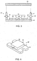
- Fig. 1 is a cross-sectional view illustrating a main portion of a heat dissipation plate for a semiconductor package according to a first embodiment.
- Fig. 2 is a plane view illustrating the plate shown in Fig. 1 .
- Fig. 3 is an exploded perspective view illustrating a semiconductor device according to a first embodiment.
- Fig. 4 is a perspective view including the semiconductor device shown in Fig. 3 .
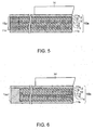
- Fig. 5 is a cross-sectional view illustrating a main portion of a heat dissipation plate according to a second embodiment.
- Fig. 6 is a cross-sectional view illustrating a main portion of a heat dissipation plate according to a third embodiment.
- Fig. 7 is a cross-sectional view illustrating a main portion of a heat dissipation plate according to a fourth embodiment.
- Fig. 8 is a cross-sectional view illustrating a main portion of a heat dissipation plate according to a fifth embodiment.
- Fig. 9 is a cross-sectional view illustrating a main portion of a heat dissipation plate according to a sixth embodiment.
- Fig. 10 is a cross-sectional view illustrating a main portion of a heat dissipation plate according to a seventh embodiment.
- a heat dissipation plate for a semiconductor package includes a lamination of a copper layer and a graphite layer, and outer copper layers, each of the outer copper layers provided to both sides of the lamination.
- Figs. 1 and 2 show a heat dissipation plate for a semiconductor device according to the first embodiment.
- Fig. 1 shows heat dissipation plate 10 on which semiconductor element 14 is mounted.
- Heat dissipation plate 10 has a flat plate structure having outer copper layers 11a, 11b at its both sides. Between outer copper layers 11a, 11b, for example, two sets of six layers of graphite layer 12, molybdenum layer 13, graphite layer 12, copper layer 11c, graphite layer 12 and copper layer 11c laminated in order, are laminated and further graphite layer 12, molybdenum 13 and graphite layer 12 are laminated in order on copper layer 12 of the second set of six layers.
- the graphite layer is excellent in thermal conductivity in a plane direction
- the copper layer is excellent in thermal conductivity in a direction vertical to a plane. That is, plural copper layers 11c, graphite layers 12, and molybdenum layers 13 are laminated alternately, and outer copper layers 11a, 11b are formed on both sides 16a and 16b of the lamination.
- Heat dissipation plate 10 has frame member 15, which is formed by laminating metal, for example, copper layer 11d and molybdenum layer 13a, at a periphery of the lamination, and each edge of graphite layer 12 is covered by frame member 15.
- Copper layers 11c, graphite layers 12, molybdenum layers 13 and outer copper layers 11a, 11b are stacked in order as mentioned above, and are subjected to pressure and heating process, and, for example, copper layer of 0.1 mm, graphite layer of 0.1 mm, molybdenum layer of 0.02mm and outer copper layers 11a and 11b of 0.2mm are laminated and integrated.
- An amount of molybdenum layers 13 is selected so that the thermal expansion coefficient of heat dissipation plate 10 becomes close to that of the ceramic substrate which constitutes the semiconductor element 14 mounted on heat dissipation plate 10.
- a ratio of a total thickness of outer copper layers 11a, 11b and copper layers 11c to a total thickness of graphite layers 12 is set as about 1.
- copper layers 11d and molybdenum layers 13a are stacked at the periphery of the lamination and between outer copper layers 11a, 11b, and are subjected to pressure and heating process, thereby copper layers 11d and molybdenum layers 13a are laminated and frame member 15 is thus formed.
- Frame member 15 is simultaneously formed, when the lamination and outer copper layers are integrated.
- the semiconductor device includes a heat dissipation plate having a lamination of copper layer, graphite layer and molybdenum layer, and outer copper layers provided on both surface of the lamination and a semiconductor element mounted on the heat dissipation pate.
- the semiconductor element includes semiconductor chip and substrate.
- the semiconductor device further includes a frame having open ends at opposite sides and outer connecting terminal. The frame member is attached to the heat dissipation plate and encompasses the semiconductor element. And a cover attached to the other open end of the frame member. And a wire connects the semiconductor element and the outer connecting terminal.
- Semiconductor device 20 shown in Figs. 3 and 4 is manufactured by preparing a treatment layer (not shown Figs. 1 and 2 ) such as a gold plating, on an outer surfaces of outer copper layers 11a, 11b, and frame member 15 of heat dissipation plate 10 shown in Fig. 1 and Fig. 2 , and mounting semiconductor element 14 on the treatment layer.
- a treatment layer such as a gold plating
- frame 21 which constitutes the semiconductor package is attached on one of outer copper layers (not shown) of heat dissipation plate 10.
- Outer connection terminals 22 pass through frame 21.
- ceramic substrate 141 and semiconductor chip 142 of semiconductor element 14 are mounted and bonded by using solder etc.
- Ceramic substrate 141 and semiconductor chip 142 are electrically connected with mutual and outer connection terminals 22 by conductive wires 24.
- Cover 23 which constitutes a semiconductor package is attached to the open end of frame 21, and thus semiconductor device 20 shown in Fig. 4 is formed.
- the thermal expansion coefficient of heat dissipation plate 10 is brought close to that of ceramic substrate 141 of semiconductor element 14 by the function of molybdenum layers 13.
- ceramic substrate 141 is bonded to heat dissipation plate 10 using solder etc., even if there is a temperature change caused by heating and cooling a bonding portion, highly precise bonding is maintained without braking ceramic substrate 141, since the thermal expansion coefficient of heat dissipation plate is brought close to that of ceramic substrate 141 and thermal deformations of heat dissipation plate 10 and ceramic substrate 141 become similar. In a same function, even if there is a temperature change of the package of semiconductor device 20, highly precise bonding is maintained without breaking the ceramic substrate 141 of a semiconductor device 14.
- heat dissipation plate 10 operates and generates heat, first the heat will be transferred to outer copper layer 11a and then the heat will be transferred to ceramic substrate 141 via outer copper layer 11a.
- thermal expansion coefficient of heat dissipation plate 10 is brought close to that of ceramic substrate 141 and heat deformations of heat dissipation plate 10 and ceramic substrate 141 are similar, highly precise bonding is maintained without braking ceramic substrate 141.
- the heat transferred to heat dissipation plate 10 is efficiently conducted in a direction vertical to a plate surface by outer copper layers 11a, 11b, copper layers 11c and frame member 15, and the heat is efficiently conducted in plane surface direction by graphite layer 12, and thereby the heat is conducted uniformly to whole the heat dissipation plate 10. Accordingly, semiconductor element 14 on heat dissipation plate 10 is efficiently heat-controlled while keeping a high precise mounting between outer copper layer 11a and semiconductor element 14.
- This invention is not limited to above-mentioned embodiment, it is possible to constitute heat dissipation plates for semiconductor packages 10a, 10b, 10c, 10d, 10e, and 10f as shown in, for example, Figs. 5, 6 , 7, 8 , 9 and 10 , and the similar effective effect are obtained. Moreover, semiconductor devices can be manufactured using these heat dissipation plates.
- the same numerals denote the same portions illustrated in Figs. 1 through 4 , and detailed explanations of those elements are omitted.
- Fig. 5 shows a heat dissipation plate for a semiconductor package according to the second embodiment.
- frame member 15a provided at a periphery is formed by laminating copper layers 11e, and other portion is formed by laminating outer copper layers 11a, 11b, copper layers 11c, graphite layers 12 and molybdenum layers 13 alternately as well as the embodiment shown in Fig. 1 .
- Fig. 6 shows a heat dissipation plate for a semiconductor package according to the third embodiment.
- frame member 15b provided at a periphery is formed of cupper, and frame member 15b and outer copper layer 11b are formed integrally.
- Fig. 7 shows a heat dissipation plate for semiconductor package according to the fourth embodiment.
- Heat dissipation plate 10c has semiconductor chip mounting portion 101a between outer copper layers 11a, 11b corresponding to area 101 which semiconductor chip 142 is mounted on, and semiconductor chip mounting portion 101a is formed by laminating copper layers 11c and molybdenum layers 13 without graphite layer 12.
- semiconductor chip mounting portion 101a the heat conductive ability in a direction vertical to a plane surface is improved by copper layer 11c and molybdenum layer 13 and a still better thermal conductivity is obtained.
- the heat from semiconductor chip 142 which heating value is concentrated in a semiconductor element, becomes possible to transfer more efficiently in the direction vertical to the plane surface.
- Fig. 8 shows a heat dissipation plate for a semiconductor package according to the fifth embodiment.
- semiconductor chip mounting portion 101b is formed by laminating copper layers 11c only without graphite layer 12 and molybdenum layer 13.
- semiconductor chip mounting portion 101b a heat conductive ability in a direction vertical to the plane surface is improved. Thereby the heat from semiconductor chip 142, which heating value is concentrated in a semiconductor element 14, becomes possible to transfer more efficiently in the direction vertical to the plane surface.
- Fig. 9 shows a heat dissipation plate for a semiconductor package according to the sixth embodiment.
- frame member 15b provided at the periphery is formed of copper only
- semiconductor chip mounting portion 101c is also formed of copper only.
- Frame member 15b, semiconductor chip mounting portion 101c and outer copper layer 11b are formed integrally.
- semiconductor chip 142 is mounted on heat dissipation plate 10e as heat dissipation plate 10d shown in Fig. 8
- Fig. 10 shows a heat dissipation plate for a semiconductor package according to the seventh embodiment.
- the first embodiment shown in Fig. 1 has frame member 15, heat dissipation plate 10f according to this embodiment does not have frame member 15.
- each molybdenum layer 13 is sandwiched by graphite layers 12 are explained.
- the invention is not limited to those embodiments, and molybdenum layer 13 may be inserted between graphite layer 12 and copper layer 11c, between outer copper layer 11a (11b) and copper layer 11c, or between copper layers 11c.
Landscapes
- Cooling Or The Like Of Semiconductors Or Solid State Devices (AREA)
Abstract
Description
- This application is based upon and claims the benefit of priority from the Japanese Patent Application No.
2007-177636, filed on July 5, 2007 - This invention relates to a heat dissipation plate used for a semiconductor package which encompasses a semiconductor element, such as various kinds of LSIs and ICs, and a semiconductor device using the heat dissipation plate.
- Generally a semiconductor element generates more heat as output power goes up. To maintain the performance of the semiconductor element, a heat dissipation plate used for a semiconductor packages has various kinds of structures.
- For example, Japanese laid-open patent application No.
2001-144237 - The above-mentioned graphite sheet lamination heat conductor can perform a high heat conduction characteristics. However, in case it is used in the semiconductor package with a ceramic substrate, a bonding part with the ceramic substrate may be damaged by a heat deformation, since the thermal expansion coefficient of the graphite sheet lamination heat conductor differs from greatly that of the ceramic substrate.
- On the other hand, Japanese patent No.
3862737 - However, the heat-conduction efficiency of the above-mentioned material is not satisfactory. When an output power of the semiconductor element goes up and a heating value rises further, it becomes difficult to cope with the increase in heating value without increasing a heat dissipation area.
- A heat dissipation plate is provided with a lamination of copper layer, molybdenum layer and graphite layer and outer copper layers each provided a surface of the lamination.
- Also, a semiconductor device includes a heat dissipation plate, a semiconductor element having semiconductor chip and substrate, a frame having open ends at opposite sides and outer connecting terminal, a cover attached to the other open end of the frame member and a wire connecting the semiconductor element and the outer connecting terminal. The heat dissipation plate includes a lamination of copper layer, molybdenum layer and graphite layer, and outer copper layers provided on both surfaces of the lamination.
-
Fig. 1 is a cross-sectional view illustrating a main portion of a heat dissipation plate for a semiconductor package according to a first embodiment. -
Fig. 2 is a plane view illustrating the plate shown inFig. 1 . -
Fig. 3 is an exploded perspective view illustrating a semiconductor device according to a first embodiment. -
Fig. 4 is a perspective view including the semiconductor device shown inFig. 3 . -
Fig. 5 is a cross-sectional view illustrating a main portion of a heat dissipation plate according to a second embodiment. -
Fig. 6 is a cross-sectional view illustrating a main portion of a heat dissipation plate according to a third embodiment. -
Fig. 7 is a cross-sectional view illustrating a main portion of a heat dissipation plate according to a fourth embodiment. -
Fig. 8 is a cross-sectional view illustrating a main portion of a heat dissipation plate according to a fifth embodiment. -
Fig. 9 is a cross-sectional view illustrating a main portion of a heat dissipation plate according to a sixth embodiment. -
Fig. 10 is a cross-sectional view illustrating a main portion of a heat dissipation plate according to a seventh embodiment. - The accompanying drawings, which are incorporated in and constitute a part of this specification, illustrate several embodiments of the invention and together with the description, serve to explain the principles of the invention.
- A heat dissipation plate for a semiconductor package according to the embodiment includes a lamination of a copper layer and a graphite layer, and outer copper layers, each of the outer copper layers provided to both sides of the lamination.
-
Figs. 1 and 2 show a heat dissipation plate for a semiconductor device according to the first embodiment.Fig. 1 showsheat dissipation plate 10 on whichsemiconductor element 14 is mounted.Heat dissipation plate 10 has a flat plate structure havingouter copper layers outer copper layers graphite layer 12,molybdenum layer 13,graphite layer 12,copper layer 11c,graphite layer 12 andcopper layer 11c laminated in order, are laminated andfurther graphite layer 12,molybdenum 13 andgraphite layer 12 are laminated in order oncopper layer 12 of the second set of six layers. The graphite layer is excellent in thermal conductivity in a plane direction, and the copper layer is excellent in thermal conductivity in a direction vertical to a plane. That is,plural copper layers 11c,graphite layers 12, andmolybdenum layers 13 are laminated alternately, andouter copper layers sides Heat dissipation plate 10 hasframe member 15, which is formed by laminating metal, for example,copper layer 11d andmolybdenum layer 13a, at a periphery of the lamination, and each edge ofgraphite layer 12 is covered byframe member 15. -
Copper layers 11c,graphite layers 12,molybdenum layers 13 andouter copper layers outer copper layers molybdenum layers 13 is selected so that the thermal expansion coefficient ofheat dissipation plate 10 becomes close to that of the ceramic substrate which constitutes thesemiconductor element 14 mounted onheat dissipation plate 10. A ratio of a total thickness ofouter copper layers copper layers 11c to a total thickness ofgraphite layers 12 is set as about 1. - Furthermore,
copper layers 11d andmolybdenum layers 13a are stacked at the periphery of the lamination and betweenouter copper layers copper layers 11d andmolybdenum layers 13a are laminated andframe member 15 is thus formed.Frame member 15 is simultaneously formed, when the lamination and outer copper layers are integrated. - A semiconductor device using the above mentioned heat dissipation plate according to the first embodiment will be explained. The semiconductor device includes a heat dissipation plate having a lamination of copper layer, graphite layer and molybdenum layer, and outer copper layers provided on both surface of the lamination and a semiconductor element mounted on the heat dissipation pate. The semiconductor element includes semiconductor chip and substrate. The semiconductor device further includes a frame having open ends at opposite sides and outer connecting terminal. The frame member is attached to the heat dissipation plate and encompasses the semiconductor element. And a cover attached to the other open end of the frame member. And a wire connects the semiconductor element and the outer connecting terminal.
-
Semiconductor device 20 shown inFigs. 3 and 4 is manufactured by preparing a treatment layer (not shownFigs. 1 and 2 ) such as a gold plating, on an outer surfaces ofouter copper layers frame member 15 ofheat dissipation plate 10 shown inFig. 1 and Fig. 2 , and mountingsemiconductor element 14 on the treatment layer. - As shown in
Fig. 3 , in the semiconductor device according to the first embodiment,frame 21 which constitutes the semiconductor package is attached on one of outer copper layers (not shown) ofheat dissipation plate 10.Outer connection terminals 22 pass throughframe 21. Onheat dissipation plate 10 withinframe 21,ceramic substrate 141 andsemiconductor chip 142 ofsemiconductor element 14 are mounted and bonded by using solder etc.Ceramic substrate 141 andsemiconductor chip 142 are electrically connected with mutual andouter connection terminals 22 byconductive wires 24.Cover 23 which constitutes a semiconductor package is attached to the open end offrame 21, and thussemiconductor device 20 shown inFig. 4 is formed. - The heat dissipation plate for semiconductor package according to the first embodiment and the semiconductor device according to the first embodiment, the thermal expansion coefficient of
heat dissipation plate 10 is brought close to that ofceramic substrate 141 ofsemiconductor element 14 by the function ofmolybdenum layers 13. Duringceramic substrate 141 is bonded toheat dissipation plate 10 using solder etc., even if there is a temperature change caused by heating and cooling a bonding portion, highly precise bonding is maintained without brakingceramic substrate 141, since the thermal expansion coefficient of heat dissipation plate is brought close to that ofceramic substrate 141 and thermal deformations ofheat dissipation plate 10 andceramic substrate 141 become similar. In a same function, even if there is a temperature change of the package ofsemiconductor device 20, highly precise bonding is maintained without breaking theceramic substrate 141 of asemiconductor device 14. - Furthermore, if
semiconductor chip 142 onouter copper layer 11a ofheat dissipation plate 10 operates and generates heat, first the heat will be transferred toouter copper layer 11a and then the heat will be transferred toceramic substrate 141 viaouter copper layer 11a. In this case, since thermal expansion coefficient ofheat dissipation plate 10 is brought close to that ofceramic substrate 141 and heat deformations ofheat dissipation plate 10 andceramic substrate 141 are similar, highly precise bonding is maintained without brakingceramic substrate 141. - Simultaneously, the heat transferred to
heat dissipation plate 10 is efficiently conducted in a direction vertical to a plate surface byouter copper layers copper layers 11c andframe member 15, and the heat is efficiently conducted in plane surface direction bygraphite layer 12, and thereby the heat is conducted uniformly to whole theheat dissipation plate 10. Accordingly,semiconductor element 14 onheat dissipation plate 10 is efficiently heat-controlled while keeping a high precise mounting betweenouter copper layer 11a andsemiconductor element 14. - As such, damage of
semiconductor element 14 mounted onheat dissipation plate 10, which is caused by the heat deformation, is prevented. Moreoverheat dissipation palate 10 having outstanding thermally conductive ability is realized, and the efficient thermal control ofsemiconductor element 14 becomes possible. - This invention is not limited to above-mentioned embodiment, it is possible to constitute heat dissipation plates for
semiconductor packages Figs. 5, 6 ,7, 8 ,9 and 10 , and the similar effective effect are obtained. Moreover, semiconductor devices can be manufactured using these heat dissipation plates. In the embodiment shown inFigs. 5 through 10 , the same numerals denote the same portions illustrated inFigs. 1 through 4 , and detailed explanations of those elements are omitted. -
Fig. 5 shows a heat dissipation plate for a semiconductor package according to the second embodiment. Inheat dissipation plate 10a,frame member 15a provided at a periphery is formed by laminatingcopper layers 11e, and other portion is formed by laminatingouter copper layers copper layers 11c, graphite layers 12 andmolybdenum layers 13 alternately as well as the embodiment shown inFig. 1 . -
Fig. 6 shows a heat dissipation plate for a semiconductor package according to the third embodiment. Inheat dissipation plate 10b,frame member 15b provided at a periphery is formed of cupper, andframe member 15b andouter copper layer 11b are formed integrally. -
Fig. 7 shows a heat dissipation plate for semiconductor package according to the fourth embodiment.Heat dissipation plate 10c has semiconductorchip mounting portion 101a betweenouter copper layers area 101 whichsemiconductor chip 142 is mounted on, and semiconductorchip mounting portion 101a is formed by laminating copper layers 11c andmolybdenum layers 13 withoutgraphite layer 12. In semiconductorchip mounting portion 101a, the heat conductive ability in a direction vertical to a plane surface is improved bycopper layer 11c andmolybdenum layer 13 and a still better thermal conductivity is obtained. Thereby the heat fromsemiconductor chip 142, which heating value is concentrated in a semiconductor element, becomes possible to transfer more efficiently in the direction vertical to the plane surface. -
Fig. 8 shows a heat dissipation plate for a semiconductor package according to the fifth embodiment. Inheat dissipation plate 10d, semiconductorchip mounting portion 101b is formed by laminating copper layers 11c only withoutgraphite layer 12 andmolybdenum layer 13. In semiconductorchip mounting portion 101b, a heat conductive ability in a direction vertical to the plane surface is improved. Thereby the heat fromsemiconductor chip 142, which heating value is concentrated in asemiconductor element 14, becomes possible to transfer more efficiently in the direction vertical to the plane surface. -
Fig. 9 shows a heat dissipation plate for a semiconductor package according to the sixth embodiment. Inheat dissipation plate 10e, as well asheat dissipation plate 10b shown inFig. 6 ,frame member 15b provided at the periphery is formed of copper only, and semiconductorchip mounting portion 101c is also formed of copper only.Frame member 15b, semiconductorchip mounting portion 101c andouter copper layer 11b are formed integrally. In this embodiment,semiconductor chip 142 is mounted onheat dissipation plate 10e asheat dissipation plate 10d shown inFig. 8 -
Fig. 10 shows a heat dissipation plate for a semiconductor package according to the seventh embodiment. Although the first embodiment shown inFig. 1 hasframe member 15,heat dissipation plate 10f according to this embodiment does not haveframe member 15. - In the above-mentioned
heat dissipation plates chip mounting portion - In each of the above-mentioned embodiments, the cases which each
molybdenum layer 13 is sandwiched bygraphite layers 12 are explained. However, the invention is not limited to those embodiments, andmolybdenum layer 13 may be inserted betweengraphite layer 12 andcopper layer 11c, betweenouter copper layer 11a (11b) andcopper layer 11c, or betweencopper layers 11c. - Other embodiments or modifications of the present invention will be apparent to those skilled in the art from consideration of the specification and practice of the invention disclosed herein. It is intended that the specification and example embodiments be considered as exemplary only, with a true scope and spirit of the invention being indicated by the following.
Claims (13)
- A heat dissipation plate, comprising:a lamination of a copper layer, a molybdenum layer and a graphite layer; and outer copper layers, each provided on a surface of the lamination.
- The heat dissipation plate according to claim 1, wherein a metal frame member is provided at a periphery of the lamination.
- The heat dissipation plate according to claim 2, wherein the metal frame member is formed of copper.
- The heat dissipation plate according to claim 2, wherein the metal frame member is formed of a combination of copper and molybdenum.
- The heat dissipation plate according to claim 1, wherein the lamination has a plurality of layers including the copper layer, the graphite layer and the molybdenum layer laminated alternately.
- The heat dissipation plate according to claim 3, wherein the metal frame member is integrally formed with one of the outer copper layers.
- The heat dissipation plate according to any preceding claim, further comprising a semiconductor chip mounting portion provided between the outer copper layers corresponding to an area for a semiconductor element to be mounted on.
- The heat dissipation plate according to claim 7, wherein the semiconductor chip mounting portion includes a lamination of copper layers.
- The heat dissipation plate according to claim 7, wherein the semiconductor chip mounting portion is formed of copper and the semiconductor chip mounting portion is integrally formed with one of the outer copper layers.
- The heat dissipation plate according to claim 7, wherein the semiconductor chip mounting portion includes a lamination of copper layers and molybdenum layers.
- The heat dissipation plate according to any preceding claim, wherein the outer copper layer is thicker than the copper layer of the lamination.
- The heat dissipation plate according to any preceding claim, wherein a ratio between a total thickness of the outer copper layers and the copper layer in the lamination, and a total thickness of the graphite layer is 1.
- A semiconductor device, comprising:a heat dissipation plate having a lamination of a copper layer, a graphite layer and a molybdenum layer, and outer copper layers each provided on a surface of the lamination;a semiconductor element mounted on the heat dissipation plate, the semiconductor element having semiconductor chip and substrate;a frame having open ends at opposite sides and outer connecting terminal, the frame being attached to the heat dissipation plate at one open end and encompassing the semiconductor element;a cover attached to the other open end of the frame member; anda wire connecting the semiconductor element and the outer connecting terminal.
Applications Claiming Priority (1)
| Application Number | Priority Date | Filing Date | Title |
|---|---|---|---|
| JP2007177636A JP4558012B2 (en) | 2007-07-05 | 2007-07-05 | Semiconductor package heat dissipation plate and semiconductor device |
Publications (2)
| Publication Number | Publication Date |
|---|---|
| EP2012355A2 true EP2012355A2 (en) | 2009-01-07 |
| EP2012355A3 EP2012355A3 (en) | 2009-09-30 |
Family
ID=39765063
Family Applications (1)
| Application Number | Title | Priority Date | Filing Date |
|---|---|---|---|
| EP08252304A Withdrawn EP2012355A3 (en) | 2007-07-05 | 2008-07-04 | Heat dissipation plate and semiconductor device |
Country Status (5)
| Country | Link |
|---|---|
| US (1) | US7745928B2 (en) |
| EP (1) | EP2012355A3 (en) |
| JP (1) | JP4558012B2 (en) |
| KR (1) | KR101015294B1 (en) |
| TW (1) | TWI438877B (en) |
Cited By (4)
| Publication number | Priority date | Publication date | Assignee | Title |
|---|---|---|---|---|
| US8034451B2 (en) | 2005-12-02 | 2011-10-11 | Morganite Electrical Carbon Limited | Carbon materials |
| WO2012139935A1 (en) * | 2011-04-12 | 2012-10-18 | BSH Bosch und Siemens Hausgeräte GmbH | Cooling device for an electronic module of a household appliance, and assembly and domestic appliance comprising a cooling device |
| WO2015055899A1 (en) * | 2013-10-18 | 2015-04-23 | Griset | Support for electronic power components, power module provided with such a support, and corresponding production method |
| EP3007531A4 (en) * | 2013-12-27 | 2016-08-31 | Huawei Tech Co Ltd | THERMO-CONDUCTIVE SHEET OF COMPOSITE MATERIAL AND METHOD FOR MANUFACTURING THE SAME |
Families Citing this family (17)
| Publication number | Priority date | Publication date | Assignee | Title |
|---|---|---|---|---|
| JP4768024B2 (en) * | 2006-07-28 | 2011-09-07 | 京セラ株式会社 | Electronic component storage package and electronic device |
| JP5105801B2 (en) | 2006-09-05 | 2012-12-26 | 株式会社東芝 | Semiconductor device |
| JP5112101B2 (en) * | 2007-02-15 | 2013-01-09 | 株式会社東芝 | Semiconductor package |
| US20100091477A1 (en) * | 2008-10-14 | 2010-04-15 | Kabushiki Kaisha Toshiba | Package, and fabrication method for the package |
| JP4643703B2 (en) * | 2008-11-21 | 2011-03-02 | 株式会社東芝 | Semiconductor device fixture and mounting structure thereof |
| JP2010192701A (en) * | 2009-02-18 | 2010-09-02 | Showa Denko Kk | Light emitting diode, light emitting diode lamp, and method of manufacturing the light emitting diode |
| JP5806464B2 (en) * | 2010-02-03 | 2015-11-10 | 株式会社東芝 | Semiconductor element storage package and semiconductor device using the same |
| JP5450313B2 (en) | 2010-08-06 | 2014-03-26 | 株式会社東芝 | High frequency semiconductor package and manufacturing method thereof |
| US10988630B2 (en) | 2014-12-19 | 2021-04-27 | Certainteed Corporation | Coating compositions for building materials and coated building material substrates |
| US9791704B2 (en) * | 2015-01-20 | 2017-10-17 | Microsoft Technology Licensing, Llc | Bonded multi-layer graphite heat pipe |
| US10108017B2 (en) | 2015-01-20 | 2018-10-23 | Microsoft Technology Licensing, Llc | Carbon nanoparticle infused optical mount |
| US10028418B2 (en) | 2015-01-20 | 2018-07-17 | Microsoft Technology Licensing, Llc | Metal encased graphite layer heat pipe |
| US10444515B2 (en) | 2015-01-20 | 2019-10-15 | Microsoft Technology Licensing, Llc | Convective optical mount structure |
| KR102293885B1 (en) * | 2015-02-03 | 2021-08-26 | 삼성디스플레이 주식회사 | Display device |
| IL266595B (en) | 2016-11-16 | 2022-08-01 | Magic Leap Inc | Thermal management systems for wearable components |
| EP3726572B1 (en) | 2019-04-16 | 2025-08-13 | ABB Schweiz AG | Heatsink assembly, method of manufacturing a heatsink assembly, and an electrical device |
| WO2022250382A1 (en) * | 2021-05-27 | 2022-12-01 | 주식회사 아모그린텍 | Ceramic substrate with heat sink and manufacturing method thereof |
Citations (3)
| Publication number | Priority date | Publication date | Assignee | Title |
|---|---|---|---|---|
| JP2001144237A (en) | 1999-11-18 | 2001-05-25 | Matsushita Electric Ind Co Ltd | Graphite sheet laminated thermal conductor |
| JP3862737B1 (en) | 2005-10-18 | 2006-12-27 | 栄樹 津島 | Cladding material and manufacturing method thereof, cladding material molding method, and heat dissipation substrate using cladding material |
| JP2007177636A (en) | 2005-12-27 | 2007-07-12 | Toyota Motor Corp | Fuel fuel gauge and remaining odometer control system |
Family Cites Families (20)
| Publication number | Priority date | Publication date | Assignee | Title |
|---|---|---|---|---|
| US346421A (en) * | 1886-07-27 | Brush | ||
| US328514A (en) * | 1885-10-20 | spbague | ||
| US349615A (en) * | 1886-09-21 | Signor to george westing house | ||
| US4689110A (en) * | 1983-12-22 | 1987-08-25 | Trw Inc. | Method of fabricating multilayer printed circuit board structure |
| US5224017A (en) | 1989-05-17 | 1993-06-29 | The Charles Stark Draper Laboratory, Inc. | Composite heat transfer device |
| US4963414A (en) | 1989-06-12 | 1990-10-16 | General Electric Company | Low thermal expansion, heat sinking substrate for electronic surface mount applications |
| US5276423A (en) * | 1991-11-12 | 1994-01-04 | Texas Instruments Incorporated | Circuit units, substrates therefor and method of making |
| US5156923A (en) | 1992-01-06 | 1992-10-20 | Texas Instruments Incorporated | Heat-transferring circuit substrate with limited thermal expansion and method for making |
| US5306571A (en) | 1992-03-06 | 1994-04-26 | Bp Chemicals Inc., Advanced Materials Division | Metal-matrix-composite |
| DE19605302A1 (en) | 1996-02-14 | 1997-08-21 | Fraunhofer Ges Forschung | Heatsink with a mounting surface for an electronic component |
| JP4272329B2 (en) | 2000-03-15 | 2009-06-03 | 京セラ株式会社 | Package for storing semiconductor elements |
| JP2001313345A (en) * | 2000-04-28 | 2001-11-09 | Kyocera Corp | Package for storing semiconductor elements |
| US6724079B2 (en) * | 2002-01-04 | 2004-04-20 | Motorola, Inc. | Wire bond-less electronic component for use with an external circuit and method of manufacture |
| JP2006013420A (en) * | 2004-01-28 | 2006-01-12 | Kyocera Corp | Electronic component storage package and electronic device |
| JP2005277382A (en) * | 2004-02-23 | 2005-10-06 | Kyocera Corp | Electronic component storage package and electronic device |
| JP4382547B2 (en) * | 2004-03-24 | 2009-12-16 | 株式会社アライドマテリアル | Semiconductor device substrate and semiconductor device |
| JP4711165B2 (en) * | 2004-06-21 | 2011-06-29 | 日立金属株式会社 | High thermal conductivity / low thermal expansion composite and method for producing the same |
| JP4575147B2 (en) | 2004-12-28 | 2010-11-04 | 株式会社東芝 | Semiconductor device |
| JP4610414B2 (en) | 2005-03-22 | 2011-01-12 | 京セラ株式会社 | Electronic component storage package, electronic device, and electronic device mounting structure |
| JP5105801B2 (en) | 2006-09-05 | 2012-12-26 | 株式会社東芝 | Semiconductor device |
-
2007
- 2007-07-05 JP JP2007177636A patent/JP4558012B2/en not_active Expired - Fee Related
-
2008
- 2008-06-30 US US12/164,396 patent/US7745928B2/en not_active Expired - Fee Related
- 2008-07-01 TW TW097124724A patent/TWI438877B/en not_active IP Right Cessation
- 2008-07-04 KR KR1020080064762A patent/KR101015294B1/en not_active Expired - Fee Related
- 2008-07-04 EP EP08252304A patent/EP2012355A3/en not_active Withdrawn
Patent Citations (3)
| Publication number | Priority date | Publication date | Assignee | Title |
|---|---|---|---|---|
| JP2001144237A (en) | 1999-11-18 | 2001-05-25 | Matsushita Electric Ind Co Ltd | Graphite sheet laminated thermal conductor |
| JP3862737B1 (en) | 2005-10-18 | 2006-12-27 | 栄樹 津島 | Cladding material and manufacturing method thereof, cladding material molding method, and heat dissipation substrate using cladding material |
| JP2007177636A (en) | 2005-12-27 | 2007-07-12 | Toyota Motor Corp | Fuel fuel gauge and remaining odometer control system |
Cited By (4)
| Publication number | Priority date | Publication date | Assignee | Title |
|---|---|---|---|---|
| US8034451B2 (en) | 2005-12-02 | 2011-10-11 | Morganite Electrical Carbon Limited | Carbon materials |
| WO2012139935A1 (en) * | 2011-04-12 | 2012-10-18 | BSH Bosch und Siemens Hausgeräte GmbH | Cooling device for an electronic module of a household appliance, and assembly and domestic appliance comprising a cooling device |
| WO2015055899A1 (en) * | 2013-10-18 | 2015-04-23 | Griset | Support for electronic power components, power module provided with such a support, and corresponding production method |
| EP3007531A4 (en) * | 2013-12-27 | 2016-08-31 | Huawei Tech Co Ltd | THERMO-CONDUCTIVE SHEET OF COMPOSITE MATERIAL AND METHOD FOR MANUFACTURING THE SAME |
Also Published As
| Publication number | Publication date |
|---|---|
| JP4558012B2 (en) | 2010-10-06 |
| KR101015294B1 (en) | 2011-02-15 |
| US7745928B2 (en) | 2010-06-29 |
| US20090008770A1 (en) | 2009-01-08 |
| TWI438877B (en) | 2014-05-21 |
| TW200917435A (en) | 2009-04-16 |
| JP2009016621A (en) | 2009-01-22 |
| KR20090004738A (en) | 2009-01-12 |
| EP2012355A3 (en) | 2009-09-30 |
Similar Documents
| Publication | Publication Date | Title |
|---|---|---|
| US7745928B2 (en) | Heat dissipation plate and semiconductor device | |
| US8391011B2 (en) | Cooling device | |
| CN100517696C (en) | Semiconductor device having semiconductor element, insulation substrate and metal electrode | |
| CN104603933B (en) | Power module substrate and power module | |
| US7361985B2 (en) | Thermally enhanced molded package for semiconductors | |
| US11075331B2 (en) | Thermoelectric device having circuitry with structural rigidity | |
| EP2237336A1 (en) | Thermoelectric device | |
| KR101017452B1 (en) | Semiconductor package | |
| WO2008013279A1 (en) | Electronic component storing package and electronic device | |
| TW200921871A (en) | Heat conductor | |
| JP2004022973A (en) | Ceramic circuit board and semiconductor module | |
| JP4935220B2 (en) | Power module device | |
| JP3669980B2 (en) | MODULE STRUCTURE MANUFACTURING METHOD, CIRCUIT BOARD FIXING METHOD, AND CIRCUIT BOARD | |
| WO2019163941A1 (en) | Substrate for power modules, and power module | |
| CN120356878A (en) | Clip | |
| US20140091444A1 (en) | Semiconductor unit and method for manufacturing the same | |
| JP6060053B2 (en) | Power semiconductor device | |
| WO2021085006A1 (en) | Power semiconductor device and method for manufacturing power semiconductor device | |
| JP4876612B2 (en) | Insulated heat transfer structure and power module substrate | |
| KR20250147449A (en) | heatsink | |
| JP2004096035A (en) | Method for manufacturing module structure, method for fixing circuit board, and circuit board | |
| JP6406547B2 (en) | Electronic component mounting package, electronic device, and electronic module | |
| WO2025023251A1 (en) | Heat dissipation member | |
| WO2016079970A1 (en) | Cooling module | |
| WO2023171019A1 (en) | Insulated circuit board with integrated heat sink, and electronic device |
Legal Events
| Date | Code | Title | Description |
|---|---|---|---|
| PUAI | Public reference made under article 153(3) epc to a published international application that has entered the european phase |
Free format text: ORIGINAL CODE: 0009012 |
|
| 17P | Request for examination filed |
Effective date: 20080710 |
|
| AK | Designated contracting states |
Kind code of ref document: A2 Designated state(s): AT BE BG CH CY CZ DE DK EE ES FI FR GB GR HR HU IE IS IT LI LT LU LV MC MT NL NO PL PT RO SE SI SK TR |
|
| AX | Request for extension of the european patent |
Extension state: AL BA MK RS |
|
| PUAL | Search report despatched |
Free format text: ORIGINAL CODE: 0009013 |
|
| AK | Designated contracting states |
Kind code of ref document: A3 Designated state(s): AT BE BG CH CY CZ DE DK EE ES FI FR GB GR HR HU IE IS IT LI LT LU LV MC MT NL NO PL PT RO SE SI SK TR |
|
| AX | Request for extension of the european patent |
Extension state: AL BA MK RS |
|
| 17Q | First examination report despatched |
Effective date: 20100420 |
|
| AKX | Designation fees paid |
Designated state(s): DE FR GB |
|
| GRAP | Despatch of communication of intention to grant a patent |
Free format text: ORIGINAL CODE: EPIDOSNIGR1 |
|
| STAA | Information on the status of an ep patent application or granted ep patent |
Free format text: STATUS: GRANT OF PATENT IS INTENDED |
|
| INTG | Intention to grant announced |
Effective date: 20180921 |
|
| STAA | Information on the status of an ep patent application or granted ep patent |
Free format text: STATUS: THE APPLICATION IS DEEMED TO BE WITHDRAWN |
|
| 18D | Application deemed to be withdrawn |
Effective date: 20190202 |