EP2009740A1 - Méta-matériau - Google Patents
Méta-matériau Download PDFInfo
- Publication number
- EP2009740A1 EP2009740A1 EP08159291A EP08159291A EP2009740A1 EP 2009740 A1 EP2009740 A1 EP 2009740A1 EP 08159291 A EP08159291 A EP 08159291A EP 08159291 A EP08159291 A EP 08159291A EP 2009740 A1 EP2009740 A1 EP 2009740A1
- Authority
- EP
- European Patent Office
- Prior art keywords
- layer
- base
- metamaterial
- cells
- layers
- Prior art date
- Legal status (The legal status is an assumption and is not a legal conclusion. Google has not performed a legal analysis and makes no representation as to the accuracy of the status listed.)
- Withdrawn
Links
Images


Classifications
-
- B—PERFORMING OPERATIONS; TRANSPORTING
- B82—NANOTECHNOLOGY
- B82Y—SPECIFIC USES OR APPLICATIONS OF NANOSTRUCTURES; MEASUREMENT OR ANALYSIS OF NANOSTRUCTURES; MANUFACTURE OR TREATMENT OF NANOSTRUCTURES
- B82Y20/00—Nanooptics, e.g. quantum optics or photonic crystals
-
- G—PHYSICS
- G02—OPTICS
- G02B—OPTICAL ELEMENTS, SYSTEMS OR APPARATUS
- G02B1/00—Optical elements characterised by the material of which they are made; Optical coatings for optical elements
- G02B1/002—Optical elements characterised by the material of which they are made; Optical coatings for optical elements made of materials engineered to provide properties not available in nature, e.g. metamaterials
- G02B1/007—Optical elements characterised by the material of which they are made; Optical coatings for optical elements made of materials engineered to provide properties not available in nature, e.g. metamaterials made of negative effective refractive index materials
-
- H—ELECTRICITY
- H01—ELECTRIC ELEMENTS
- H01Q—ANTENNAS, i.e. RADIO AERIALS
- H01Q15/00—Devices for reflection, refraction, diffraction or polarisation of waves radiated from an antenna, e.g. quasi-optical devices
- H01Q15/0006—Devices acting selectively as reflecting surface, as diffracting or as refracting device, e.g. frequency filtering or angular spatial filtering devices
- H01Q15/0086—Devices acting selectively as reflecting surface, as diffracting or as refracting device, e.g. frequency filtering or angular spatial filtering devices said selective devices having materials with a synthesized negative refractive index, e.g. metamaterials or left-handed materials
Definitions
- the invention relates to a metamaterial having a multiplicity of repetitive basic cells, each of which has a three-dimensional interconnect structure which, for electromagnetic waves with wave propagation directions pointing in three spatial dimensions, exhibits the transmission behavior characteristic of the metamaterial.
- Such a metamaterial is from the WO 2007/073716 A1 known.
- the known metamaterial is composed of a plurality of basic cells each having a plurality of gates with two poles each. The poles of the gates are connected within the basic cell via coupling capacitances and inductive lines.
- electromagnetic waves can be transmitted in any spatial direction with the transmission behavior characteristic of the property as metamaterial.
- Metamaterials are artificial structures which have in certain frequency ranges both effective dielectric coefficients and effective permeability coefficients which are less than 1 or even negative.
- a detailed overview of metamaterials is given, for example, in the publication of LAI, A. and ITOH, T .: Composite right / left-handed transmission line metamaterials, in IEEE, Microwave Magazine, September 2004, pages 34-50 given.
- Metamaterials can be used to construct lenses whose resolution is below the resolution limit of ⁇ / 2. Furthermore, antennas are conceivable which have a higher sensitivity than conventional antennas. Finally, it also seems possible to use metamaterials on a body impinging radiation to guide around the body without reflection, so that the body is not based on the back reflected or scattered portions of the incident electromagnetic radiation can be detected. However, the use of metamaterials in practice requires that the metamaterials can be manufactured effectively because large numbers of basic cells are needed for practical use.
- the invention is therefore an object of the invention to provide a metamaterial that can be made in a simple manner with a variety of basic cells.
- the conductor track structure of a basic cell is distributed on at least three interconnect layers arranged one above the other in a stack.
- basic cells should be understood as meaning the smallest three-dimensional structural unit that periodically repeats in the metamaterial.
- the layer sequence of a base cell is repeated in the stacking direction at periodic intervals. In this way, it is possible to form a plurality of basic cells stacked one above the other.
- Dielectric spacer layers are preferably arranged between the interconnect layers of the interconnect structure. Such dielectric spacer layers can be produced in a simple manner using conventional materials which are used in semiconductor and microsystem technology.
- the space between the conductor layers is completely filled by the dielectric spacer layers.
- the conductor track structure of a base cell is invariant against the point symmetry group D 4h , since, in particular, cubic conductor track structures of the point symmetry group O h can be reproduced with such a track structure. It should be noted that the point symmetry groups are given here and below in Schönflies notation.
- Such a basic cell has a base layer, an intermediate layer and a cover layer.
- capacitive surfaces are respectively arranged in the corners of the base cell and are connected via inductive components to a common node arranged in the intermediate layer.
- the coupling between juxtaposed basic cells can be accomplished in each case in the base layer and cover layer by means of interdigital capacitances between the strip conductor structures of the basic cells.
- the coupling between stacked base cells then takes place between the capacitance surfaces of the base layer and the cover layer.
- the conductor track structure of the base cell is invariant against the point symmetry group S 2 .
- the conductor track structure of cubic basic cells can be imitated with the point symmetry group T H.
- Such a metamaterial has an intermediate layer arranged between the base layer and the cover layer, in which there are two adjacent capacitance surfaces which are coupled via an inductive component.
- capacitive surfaces are formed, which are capacitively coupled to the capacitance surfaces of the intermediate layer.
- the capacitance surfaces formed in the base layer and the cover layer are in turn connected by inductive components, each with an associated capacitance area located below the base layer or above the cover layer.
- the latter capacity surfaces are in coupling layers of which one is below the base layer and another above the cover layer.
- the coupling to neighboring basic cells is produced by means of interdigital capacitances.
- the inductive elements may be, in particular, thin strip conductors, the course of which is adapted to the respectively required inductance. Furthermore, additional inductive components can be provided to increase the inductance.
- the inductive components may also include vias through the dielectric spacers.
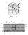
- FIG. 1 shows the perspective view of the conductor track structure of a three-dimensional basic cell 1 of a metamaterials.
- the basic cell 1 represents the smallest structural unit that continues periodically in the metamaterial.
- conductor track structure is as such from the WO 2007/073716 A1 known.
- the basic cell 1 is cube-shaped and has a central node 2. From node 2 lead from inductive lines 3 Corners 4 of the basic cell 1. In the region of the corners 4, the inductive lines 3 are connected to capacitive surfaces 5. In each case, four capacitance surfaces 5 connected to different inductive lines 3 are arranged on a side surface 6 of the basic cell 1. Contrary to the illustration in FIG. 1 are the capacity surfaces 5 only in the corners 4 with each other and connected to the inductive lines 3. Otherwise, the capacity surfaces 5 along edges 7 of the base cell 1 are separated from each other.
- a metamaterial By a plurality of side by side and optionally also superimposed basic cells of the type of basic cell 1, a metamaterial is obtained, which has a negative refractive index or a refractive index of less than 1 in a certain frequency range.
- the production of the metamaterial in practice is not easy, since a very large number of basic cells 1 must be made and interconnected.
- metamaterials must be prepared in which the number of basic cells 1 is on the order of 10 5 .
- FIG. 2 shows a cross section through a base cell 8 of a Metamaterials, the conductor track structure has a layered planar structure.
- the basic cell comprises four dielectric layers 9 of dielectric material, which are individually referred to one after another in the stacking direction as d 1 , d 2 , d 3 , d 4 .
- the layers d 1 and d 4 have the dielectric constant ⁇ 2 , and the layers d 2 and d 3 the dielectric constant ⁇ 1 .
- the layers d 1 and d 4 have the thickness h 2 and the layers d 2 and d 3 each have the thickness h 1 .
- a lower coupling layer 11 In the stacking direction at the bottom is a lower coupling layer 11, followed by a base layer 12, an intermediate layer 13, a cover layer 14 and an upper coupling layer 15.
- the lower coupling layer 11, the base layer 12, the intermediate layer 13, the cover layer 14 and the upper coupling layer 15 are in FIG. 2 each indexed with m 1 to m 5 . It should be noted that in this context height information in each case relate to the stacking direction.
- the metallization layers 10 can be applied to the dielectric layers 9 by the usual methods of semiconductor and microsystem technology and patterned there. In addition, the metallization layers 10 may be connected across the dielectric layers 9 by way of via 16.
- FIG. 3 contains a representation of the metallization layers 10 and of those dielectric layers 9 in which plated-through holes 16 are formed.
- the metallization layer m 1 which is equal to the lower coupling layer 11, four capacitance surfaces 17 are formed, which in FIG. 3 labeled P1A, P1B, P1C and P1D.
- the capacitance surfaces 17 continue into the adjacent base cells 8, so that four basic cells 1 adjoining each other in a corner 18 have a common capacitance area 17.
- the metallization layer m 2 which is separated from the metallization layer m 1 by the dielectric layer d 1 , further capacitance areas 19 are arranged, which in FIG. 3 bear the designation P2A, P2B, P2C, P2D.
- the capacitance areas 19 are each connected to inductive lines 20, which are freed in the area of the capacitance areas 19.
- the inductive lines 20 are in FIG. 3 also referred to as SP2A to SP2D.
- the inductive lines 20 open into the plated-through holes 16, marked in FIG. 13 with V2A to V2D.
- the plated-through holes 16 pass through the dielectric layer d 2 and open into a node surface 21, which in FIG. 3 designated P3A.
- the dielectric layer d 3 with the plated-through holes 16 and the metallization layers m 4 and m 5 that correspond to the cover layer 14 and the upper coupling layer 15 are symmetrical with respect to the metallization layer m 3 the dielectric layer d 2 and the metallization layers m 2 and m 1 constructed.
- the basic cell 8 is made to the basic cell 1 FIG. 1 electrically equivalent.
- the basic cell 1 is imaged with the point symmetry O h on the planar conductor track structure of the basic cell 8 with the point symmetry D 4h .
- capacitance area 17 labeled P1A capacitively couples capacitance area 19 located above capacitance area 17 labeled P2A to underlying capacitance area 19 designated P4A of the underlying basic cell 8.
- the metallizations in the lower coupling layer 11 and the lower coupling layer 15 are identical, wherein the upper coupling layer 15 of a lower-lying base cell 8 is equal to the lower coupling layer 11 of an overhead base cell 8. It is therefore only necessary to form either the lower coupling layer 11 or the upper coupling layer 15 in each basic cell 8.
- FIG. 4 For example, the structure of the base layer 12 is shown in four adjacent base cells 8.
- FIG. 5 shows the structuring of the lower coupling layer 11 of four adjacent basic cells 8.
- the affiliation to the individual basic cells is in the FIGS. 4 and 5 each indicated by the index running from one to four.
- the capacitive surfaces 17 with the designations P1D 1 , P1B 2 , P1A 4 and P1C 3 of four adjacent basic cells 8 form a contiguous metallization surface.
- This metallization surface capacitively couples the overlying capacitance surfaces 19 with the designations P2D 1 , P2B 2 , P1A 4 and P2C 3 and the underlying coupling surfaces 19 with the designations P4D 1 , P4B 2 , P4A 4 and P4C 3 .
- FIG. 6 a layer sequence of a modified basic cell 22 is shown, in which the lower coupling layer 11 and the upper coupling layer 15 have been dispensed with.
- capacitive surfaces 19 are replaced by capacitive surfaces 23 in the base cell 22, on whose outer edges interdigital structure 24 are formed.
- FIG. 7 the metallization of the lower coupling layer 11 of four side by side arranged basic cells 22 is shown. Based FIG. 7 It can be seen how the capacitance area 23 with the designation P2D 2 is coupled to the capacitance area 23 with the designation P2C 4 by the interdigital structure 24. In addition, the coupling of the capacitance areas 23 with the designation P2B 2 , P2A 4 , P2D 1 and P2C 3 can be recognized by the interdigital structure 24. The capacitive coupling of the base cells 22 in the stacking direction takes place directly between the capacitive surfaces 23, so that the dielectric layers 9 with the designation d 1 and d 4 can be combined to form a common dielectric layer 9. This offers the additional advantage that the requirements for the tolerances in the production of the dielectric layers 9 can be relaxed since only one dielectric layer 9 has to be manufactured.
- FIG. 8 shows a dispersion diagram showing the results of simulation calculations for determining the dispersion relation for a meta-material with basic cells 8.
- the abscissa represents the frequency, while the ordinate represents the phase rotation ⁇ .
- ⁇ k z ⁇ a, where a is the extent of the base cell 1 along the z-direction, which is equal to the stacking direction.
- Two different simulation programs were used for the simulation, the results of which each with dashed lines and solid lines in the diagram in FIG. 8 are registered.
- FIG. 8 It can be seen that in addition to the right-handed modes 25 and a numerical artifact 26, a left-handed mode 27 is present in the frequency range between 600 and 800 MHz.
- the left-handed mode shows a negative slope, resulting in a negative group speed.
- a negative group velocity is typical for negative refractive index metamaterials.
- a metamaterial prepared on the basis of the base cell 8 has, in a certain frequency range, the transmission behavior typical of metamaterials. Similar results are obtained in a study of wave propagation in the x-direction and y-direction, which extend in the layer plane. Thus, a metamaterial prepared on the basis of the base cell 8 has a transmission characteristic typical of metamaterials not only in wave propagation along the layer plane but also in wave propagation in the stacking direction.
- FIG. 9 is a partial view of another interconnect structure of another basic cell 28.
- the complete interconnect structure of in FIG. 9 basic cell 28 comprises six of these substructures 29.
- Each of the substructures 29 has an inductive line 31 running along the diagonal on an outer surface 30.
- the inductive lines 39 are arranged so that the inductive lines 39 extend parallel on opposite outer sides 30.
- the inductive lines 31 each connect two triangular capacitance surfaces 32, each of which faces an associated capacitance surface 32 of an adjacent substructure 29.
- the two capacitance surfaces 32 of a substructure 29 run as if they were each on a side surface 33 of a Arranged pyramid 34 whose base coincides with the outside 30 of the base cell 28.
- the opposing capacity surfaces 32 are arranged at a distance 35. Furthermore, the capacitive surfaces 32 are spaced along the edges of the pyramid 34.
- FIG. 10 the layers of a base cell 36 are shown, with which the trace structure of the base cell 28 from FIG. 9 can be realized in a planar layer structure.
- the base cell 36 has in the coupling layer 11 four capacitive surfaces 37 extending along the outer edges of the base cell 36, of which two are capacitively coupled by an interdigital structure 38.
- the capacitance surfaces 37 are connected via a further interdigital structure 39 both with plated-through holes 40, which lead to the overlying base layer 12, and with lead-throughs 41, which lead to an underlying cover layer 14.
- the plated-through holes 40 are connected to two respective dovetail-shaped capacitance surfaces 42.
- the capacity surfaces 42 are arranged facing each other with the convex inner side.
- the convex inner side of the capacitance surfaces 42 extends along the diagonal of the base cell 36, respectively.
- the capacitance surfaces 42 cover or overlap with capacitance surfaces 43 formed in the intermediate layer 13.
- the in the basic cell 36 according to FIG. 10 also dovetail-shaped capacitance surfaces 43 are connected by a central inductive line 44, which are each attached to the inflection point of the convex inner side of the capacitance surfaces 43.
- In the overlying cover layer 14 are finally more capacity areas 45, which coincide with the capacity areas 43 or at least partially overlay.
- the capacitance surfaces 45 are also formed dovetailed.
- the capacity surfaces 45 are finally on the vias 41 with an in FIG. 10 Connected not shown further coupling layer whose metallization of the metallization of the coupling layer 11 corresponds.
- FIG. 11 shows a further base cell 47, in which between the lower coupling layer 11 and the base layer 12, a lower inner coupling layer 48 and between the upper layer 14 and upper coupling layer 15, an upper inner coupling layer 49 is retracted.
- the electrodes 37 are arranged with the leading to adjacent base cells 47 inductive lines 46.
- congruent capacitance surfaces 50 are arranged in each case with the capacitance surfaces 37 in the lower outer coupling layer 11 and the upper outer coupling layer 15, which are connected by capacitive connecting pieces 51 to two pairs.
- FIG. 11 the basic cell 47 in FIG. 11 is shown completely. In a periodic repetition of the base cell 47 in the stacking direction is the lower External coupling layer 11 of the upper base cell 47 at the same height as an upper outer coupling layer 15 of the lower base cell 47. Insofar takes place in the common altitude of the lower outer coupling layer 11 and the upper outer coupling layer 15, a coupling with sibling basic cells in all four directions instead, in FIG. 11 according to the front, back, left and right. In the FIG. 11 In each case, half of the inductive lines leading to the left and right represent left and right-pointing inductive lines.
- the base cell 28, which has the point symmetry group T h is mapped into a planar printed conductor structure having the point symmetry group S 2 by the basic cells 36 and 47.
- the basic cells described herein are suitable for mass production by conventional methods of semiconductor and microsystem techniques, so that the metamaterials with the basic cells described herein can be manufactured on an industrial scale.
- a metamaterial with the basic cells 8, 22, 36 and 47 has a similar transmission behavior as a metamaterial, which is composed of the basic cells 1 and 28 and which shows in each wave propagation direction in a certain frequency range typical for a metamaterial transmission behavior.
- the interconnect structure of the respective metamaterial is preferably designed such that the basic cells 8, 22, 36 or 47 repeat in all three spatial directions.
Landscapes
- Physics & Mathematics (AREA)
- Optics & Photonics (AREA)
- Chemical & Material Sciences (AREA)
- Engineering & Computer Science (AREA)
- Nanotechnology (AREA)
- General Physics & Mathematics (AREA)
- Life Sciences & Earth Sciences (AREA)
- Biophysics (AREA)
- Crystallography & Structural Chemistry (AREA)
- Aerials With Secondary Devices (AREA)
Applications Claiming Priority (1)
| Application Number | Priority Date | Filing Date | Title |
|---|---|---|---|
| DE102007029691 | 2007-06-27 |
Publications (1)
| Publication Number | Publication Date |
|---|---|
| EP2009740A1 true EP2009740A1 (fr) | 2008-12-31 |
Family
ID=39760897
Family Applications (1)
| Application Number | Title | Priority Date | Filing Date |
|---|---|---|---|
| EP08159291A Withdrawn EP2009740A1 (fr) | 2007-06-27 | 2008-06-27 | Méta-matériau |
Country Status (1)
| Country | Link |
|---|---|
| EP (1) | EP2009740A1 (fr) |
Cited By (1)
| Publication number | Priority date | Publication date | Assignee | Title |
|---|---|---|---|---|
| CN110690576A (zh) * | 2019-09-03 | 2020-01-14 | 北京航空航天大学青岛研究院 | 基于超材料三维结构实现电磁波调制的装置及方法 |
Citations (4)
| Publication number | Priority date | Publication date | Assignee | Title |
|---|---|---|---|---|
| WO2004025783A1 (fr) * | 2002-09-14 | 2004-03-25 | Bae Systems Plc | Structure electromagnetique periodique |
| WO2006023195A2 (fr) * | 2004-07-23 | 2006-03-02 | The Regents Of The University Of California | Metamateriaux |
| US20060243925A1 (en) * | 2005-05-02 | 2006-11-02 | Raytheon Company | Smith-Purcell radiation source using negative-index metamaterial (NIM) |
| WO2007073716A1 (fr) | 2005-12-13 | 2007-07-05 | Technische Universität München | Unite de base et dispositif pour transmettre des champs electromagnetiques |
-
2008
- 2008-06-27 EP EP08159291A patent/EP2009740A1/fr not_active Withdrawn
Patent Citations (4)
| Publication number | Priority date | Publication date | Assignee | Title |
|---|---|---|---|---|
| WO2004025783A1 (fr) * | 2002-09-14 | 2004-03-25 | Bae Systems Plc | Structure electromagnetique periodique |
| WO2006023195A2 (fr) * | 2004-07-23 | 2006-03-02 | The Regents Of The University Of California | Metamateriaux |
| US20060243925A1 (en) * | 2005-05-02 | 2006-11-02 | Raytheon Company | Smith-Purcell radiation source using negative-index metamaterial (NIM) |
| WO2007073716A1 (fr) | 2005-12-13 | 2007-07-05 | Technische Universität München | Unite de base et dispositif pour transmettre des champs electromagnetiques |
Non-Patent Citations (4)
| Title |
|---|
| GRBIC ANTHONY ET AL: "An isotropic three-dimensional negative-refractive-index transmission-line metamaterial", JOURNAL OF APPLIED PHYSICS, AMERICAN INSTITUTE OF PHYSICS. NEW YORK, US, vol. 98, no. 4, 22 August 2005 (2005-08-22), pages 43106 - 043106, XP012078340, ISSN: 0021-8979 * |
| HOEFER W ET AL: "Topology and Design of Wide-Band 3D Metamaterials Made of Periodically Loaded Transmission Line Arrays", MICROWAVE SYMPOSIUM DIGEST, 2005 IEEE MTT-S INTERNATIONAL LONG BEACH, CA, USA 12-17 JUNE 2005, PISCATAWAY, NJ, USA,IEEE, 12 June 2005 (2005-06-12), pages 313 - 316, XP010844474, ISBN: 978-0-7803-8846-8 * |
| IYER, A. K.; ELEFTHE-RIADES, G. V.: "Volumetric layered transmission-line metamaterial exhibiting a negative refractive index", J. OPT. SOC. AM. B, vol. 23, no. 3, March 2006 (2006-03-01), pages 553 - 580, XP055128363, DOI: doi:10.1364/JOSAB.23.000553 |
| LAI, A.; ITOH, T.: "Composite right/left-handed transmission line metamaterials", IEEE, MICROWAVE MAGAZIN, September 2004 (2004-09-01), pages 34 - 50, XP011119759 |
Cited By (1)
| Publication number | Priority date | Publication date | Assignee | Title |
|---|---|---|---|---|
| CN110690576A (zh) * | 2019-09-03 | 2020-01-14 | 北京航空航天大学青岛研究院 | 基于超材料三维结构实现电磁波调制的装置及方法 |
Similar Documents
| Publication | Publication Date | Title |
|---|---|---|
| EP2143117B1 (fr) | Composant électrique multicouche comportant une structure de blindage sans contact électrique | |
| DE4008507C2 (de) | Laminiertes LC-Filter | |
| DE60114200T2 (de) | Keramischer vielschichtkondensatornetzwerk | |
| DE2714426C3 (de) | Als Tiefpaß- oder als Laufzeitglied ausgebildetes passives Schaltungsglied | |
| DE102009028629A1 (de) | Ultra-Breitband-Kondensator | |
| DE2045560A1 (de) | Rechteckiger Hohlleiterresonator und mit solchen Resonatoren aufgebautes Mikrowellenfilter | |
| DE3425232A1 (de) | Mehrschicht-keramikkondensator | |
| DE4021634A1 (de) | Rauschfilter | |
| DE3144026A1 (de) | "transformator" | |
| EP0298306A2 (fr) | Matériau de camouflage au radar | |
| DE1940036C3 (de) | Stirnkontaktiertes kapazitives Netzwerk | |
| DE10212868A1 (de) | Halbleitervorrichtung und Verfahrfen für ihre Herstellung | |
| DE102007013751A1 (de) | Tiefpassfilter und Tiefpassfilter-Anordnung | |
| EP2009740A1 (fr) | Méta-matériau | |
| DE3142949A1 (de) | Josephson-element und verfahren zu seiner herstellung | |
| EP1776725A2 (fr) | Transformateur piezo-electrique | |
| DE102005045638B4 (de) | Mit Oberflächenwellen arbeitender Wandler | |
| DE202008006222U1 (de) | Metamaterial | |
| DE112018005526B4 (de) | Schallwellenvorrichtung und Verfahren zur Herstellung einer Schallwellenvorrichtung | |
| DE112020006270T5 (de) | Frequenzselektives oberflächenelement, frequenzselektive oberfläche und elektromagnetische-welle-absorber | |
| EP2054953B1 (fr) | Piézotransformateur | |
| DE3731165C2 (fr) | ||
| DE4234486C1 (de) | Anordnung zum Zerlegen eines optischen Eingangssignals in zwei Signale mit zueinander orthogonaler Polarisation | |
| DE102004020167A1 (de) | Hochfrequenz-Resonatorsystem mit optimierter Stromverteilung in den Leiterelementen | |
| EP2465123B1 (fr) | Composant électrique multicouche |
Legal Events
| Date | Code | Title | Description |
|---|---|---|---|
| PUAI | Public reference made under article 153(3) epc to a published international application that has entered the european phase |
Free format text: ORIGINAL CODE: 0009012 |
|
| AK | Designated contracting states |
Kind code of ref document: A1 Designated state(s): AT BE BG CH CY CZ DE DK EE ES FI FR GB GR HR HU IE IS IT LI LT LU LV MC MT NL NO PL PT RO SE SI SK TR |
|
| AX | Request for extension of the european patent |
Extension state: AL BA MK RS |
|
| 17P | Request for examination filed |
Effective date: 20090427 |
|
| 17Q | First examination report despatched |
Effective date: 20090602 |
|
| AKX | Designation fees paid |
Designated state(s): AT BE BG CH CY CZ DE DK EE ES FI FR GB GR HR HU IE IS IT LI LT LU LV MC MT NL NO PL PT RO SE SI SK TR |
|
| STAA | Information on the status of an ep patent application or granted ep patent |
Free format text: STATUS: THE APPLICATION IS DEEMED TO BE WITHDRAWN |
|
| 18D | Application deemed to be withdrawn |
Effective date: 20120103 |