EP2009740A1 - Metamaterial - Google Patents
Metamaterial Download PDFInfo
- Publication number
- EP2009740A1 EP2009740A1 EP08159291A EP08159291A EP2009740A1 EP 2009740 A1 EP2009740 A1 EP 2009740A1 EP 08159291 A EP08159291 A EP 08159291A EP 08159291 A EP08159291 A EP 08159291A EP 2009740 A1 EP2009740 A1 EP 2009740A1
- Authority
- EP
- European Patent Office
- Prior art keywords
- layer
- base
- metamaterial
- cells
- layers
- Prior art date
- Legal status (The legal status is an assumption and is not a legal conclusion. Google has not performed a legal analysis and makes no representation as to the accuracy of the status listed.)
- Withdrawn
Links
Images


Classifications
-
- B—PERFORMING OPERATIONS; TRANSPORTING
- B82—NANOTECHNOLOGY
- B82Y—SPECIFIC USES OR APPLICATIONS OF NANOSTRUCTURES; MEASUREMENT OR ANALYSIS OF NANOSTRUCTURES; MANUFACTURE OR TREATMENT OF NANOSTRUCTURES
- B82Y20/00—Nanooptics, e.g. quantum optics or photonic crystals
-
- G—PHYSICS
- G02—OPTICS
- G02B—OPTICAL ELEMENTS, SYSTEMS OR APPARATUS
- G02B1/00—Optical elements characterised by the material of which they are made; Optical coatings for optical elements
- G02B1/002—Optical elements characterised by the material of which they are made; Optical coatings for optical elements made of materials engineered to provide properties not available in nature, e.g. metamaterials
- G02B1/007—Optical elements characterised by the material of which they are made; Optical coatings for optical elements made of materials engineered to provide properties not available in nature, e.g. metamaterials made of negative effective refractive index materials
-
- H—ELECTRICITY
- H01—ELECTRIC ELEMENTS
- H01Q—ANTENNAS, i.e. RADIO AERIALS
- H01Q15/00—Devices for reflection, refraction, diffraction or polarisation of waves radiated from an antenna, e.g. quasi-optical devices
- H01Q15/0006—Devices acting selectively as reflecting surface, as diffracting or as refracting device, e.g. frequency filtering or angular spatial filtering devices
- H01Q15/0086—Devices acting selectively as reflecting surface, as diffracting or as refracting device, e.g. frequency filtering or angular spatial filtering devices said selective devices having materials with a synthesized negative refractive index, e.g. metamaterials or left-handed materials
Abstract
Description
Die Erfindung betrifft ein Metamaterial mit einer Vielzahl von sich wiederholenden Basiszellen, die jeweils eine dreidimensionale Leiterbahnstruktur aufweisen, die für elektromagnetische Wellen mit in drei Raumdimensionen weisenden Wellenausbreitungsrichtungen das für das Metamaterial charakteristische Transmissionsverhalten zeigt.The invention relates to a metamaterial having a multiplicity of repetitive basic cells, each of which has a three-dimensional interconnect structure which, for electromagnetic waves with wave propagation directions pointing in three spatial dimensions, exhibits the transmission behavior characteristic of the metamaterial.
Ein derartiges Metamaterial ist aus der
Metamateriale sind künstliche Strukturen, welche in bestimmten Frequenzbereichen sowohl effektive Dielektrizitätskoeffizienten als auch effektive Permeabilitätskoeffizienten aufweisen, die kleiner 1 oder auch negativ sind. Eine ausführliche Übersicht über Metamaterialien wird zum Beispiel in der Veröffentlichung von
Mithilfe von Metamaterialien lassen sich grundsätzlich Linsen konstruieren, deren Auflösung unterhalb der Auflösungsgrenze von λ/2 liegt. Ferner sind Antennen denkbar, die eine höhere Empfindlichkeit als herkömmliche Antennen aufweisen. Schließlich erscheint es auch möglich, mit Metamaterialien auf einen Körper auftreffende Strahlung reflektionsfrei um den Körper herumzuführen, so dass der Körper nicht anhand der zurück reflektierten oder gestreuten Anteile der einfallenden elektromagnetischen Strahlung detektiert werden kann. Die Verwendung von Metamaterialien in der Praxis setzt jedoch voraus, dass die Metamaterialien effektiv gefertigt werden können, da für die praktische Anwendung große Stückzahlen von Basiszellen benötigt werden.Metamaterials can be used to construct lenses whose resolution is below the resolution limit of λ / 2. Furthermore, antennas are conceivable which have a higher sensitivity than conventional antennas. Finally, it also seems possible to use metamaterials on a body impinging radiation to guide around the body without reflection, so that the body is not based on the back reflected or scattered portions of the incident electromagnetic radiation can be detected. However, the use of metamaterials in practice requires that the metamaterials can be manufactured effectively because large numbers of basic cells are needed for practical use.
Weiter ist aus der
Ausgehend von diesem Stand der Technik liegt der Erfindung daher die Aufgabe zugrunde, ein Metamaterial zu schaffen, das auf einfache Weise mit einer Vielzahl von Basiszellen gefertigt werden kann.Based on this prior art, the invention is therefore an object of the invention to provide a metamaterial that can be made in a simple manner with a variety of basic cells.
Diese Aufgabe wird durch ein Metamaterial mit den Merkmalen des unabhängigen Anspruchs gelöst. In davon abhängigen Ansprüchen sind vorteilhafte Ausgestaltungen und Weiterbildungen angegeben.This object is achieved by a metamaterial having the features of the independent claim. In dependent claims advantageous embodiments and developments are given.
Bei dem Metamaterial ist die Leiterbahnstruktur einer Basiszelle auf wenigsten drei in einem Stapel übereinander angeordneten Leiterbahnenschichten verteilt. Unter Basiszellen soll in diesem Zusammenhang die kleinste sich im Metamaterial periodisch wiederholende dreidimensionale Struktureinheit verstanden werden. Durch die Verteilung der Leiterbahnstruktur der Basiszelle auf wenigstens drei in einem Stapel übereinander angeordnete Leiterbahnschichten ist es möglich, dreidimensionale Leiterbahnstrukturen von Basiszellen, die gegenüber elektromagnetischen Wellen das für die Eigenschaft als Metamaterial charakteristische Transmissionsverhalten in mehr als zwei Dimensionen zeigen, in einen Stapel von Leiterbahnschichten abzubilden, der mit den üblichen Verfahren der Halbleiter- und Mikrosystemtechnik hergestellt werden kann. Mithilfe dieser Verfahren lässt sich insbesondere eine Großzahl von Leiterbahnstrukturen verschiedener Basiszellen nebeneinander und übereinander ausbilden. Insofern ist das Metamaterial auf einfache Weise mit einer Vielzahl von Basiszellen herstellbar.In the case of the metamaterial, the conductor track structure of a basic cell is distributed on at least three interconnect layers arranged one above the other in a stack. In this context, basic cells should be understood as meaning the smallest three-dimensional structural unit that periodically repeats in the metamaterial. By distributing the conductor track structure of the base cell to at least three interconnect layers arranged in a stack, it is possible to form three-dimensional interconnect structures of basic cells which exhibit in electromagnetic waves the transmission behavior characteristic of the metamaterial in more than two dimensions, into a stack of interconnect layers which can be produced by the usual methods of semiconductor and microsystems technology. In particular, a large number of printed conductor structures of different basic cells can be formed next to and above one another using these methods. In this respect, the metamaterial can be produced in a simple manner with a large number of basic cells.
Bei einer Ausführungsform des Metamaterials wiederholt sich die Schichtenfolge einer Basiszelle in Stapelrichtung in periodischen Abständen. Auf diese Weise ist es möglich, eine Vielzahl von Basiszellen übereinander gestapelt auszubilden.In one embodiment of the metamaterial, the layer sequence of a base cell is repeated in the stacking direction at periodic intervals. In this way, it is possible to form a plurality of basic cells stacked one above the other.
Zwischen den Leiterbahnschichten der Leiterbahnstruktur sind vorzugsweise dielektrische Abstandsschichten angeordnet. Derartige dielektrische Abstandsschichten sind mit üblichen Materialien, die in der Halbleiter- und Mikrosystemtechnik verwendet werden, auf einfache Weise herstellbar.Dielectric spacer layers are preferably arranged between the interconnect layers of the interconnect structure. Such dielectric spacer layers can be produced in a simple manner using conventional materials which are used in semiconductor and microsystem technology.
In der Regel wird dabei der Raum zwischen den Leiterschichten vollständig von den dielektrischen Abstandsschichten gefüllt.As a rule, the space between the conductor layers is completely filled by the dielectric spacer layers.
Bei einer bevorzugten Ausführungsform ist die Leiterbahnstruktur einer Basiszelle invariant gegen die Punktsymmetriegruppe D4h, da sich mit einer derartigen Leiterbahnstruktur insbesondere kubische Leiterbahnstrukturen der Punktsymmetriegruppe Oh nachbilden lassen. Es sei angemerkt, dass die Punktsymmetriegruppen hier und im Folgenden in der Schönflies-Notation angegeben sind.In a preferred embodiment, the conductor track structure of a base cell is invariant against the point symmetry group D 4h , since, in particular, cubic conductor track structures of the point symmetry group O h can be reproduced with such a track structure. It should be noted that the point symmetry groups are given here and below in Schönflies notation.
Eine derartige Basiszelle verfügt über eine Grundschicht, eine Zwischenschicht und eine Deckschicht. In der Grundschicht und in der Deckschicht sind in den Ecken der Basiszelle jeweils Kapazitätsflächen angeordnet, die über induktive Komponenten mit einem in der Zwischenschicht angeordneten gemeinsamen Knotenpunkt verbunden sind.Such a basic cell has a base layer, an intermediate layer and a cover layer. In the base layer and in the cover layer, capacitive surfaces are respectively arranged in the corners of the base cell and are connected via inductive components to a common node arranged in the intermediate layer.
Die Koppelung zwischen nebeneinander angeordneten Basiszellen kann jeweils in der Grundschicht und Deckschicht mithilfe von interdigitalen Kapazitäten zwischen den Leiterbahnstrukturen der Basiszellen bewerkstelligt werden. Die Koppelung zwischen übereinander angeordneten Basiszellen erfolgt dann zwischen den Kapazitätsflächen der Grundschicht und der Deckschicht.The coupling between juxtaposed basic cells can be accomplished in each case in the base layer and cover layer by means of interdigital capacitances between the strip conductor structures of the basic cells. The coupling between stacked base cells then takes place between the capacitance surfaces of the base layer and the cover layer.
Daneben ist es möglich, zwischen der Grundschicht und der Deckschicht von in Stapelrichtung übereinander angeordnete Basiszellen eine weitere Koppelschicht vorzusehen, in der Kapazitätsflächen ausgebildet sind, die die Kapazitätsflächen, die in der Grundschicht und in der Deckschicht in den Ecken benachbarter Basiszellen angeordnet sind, kapazitiv koppeln. Durch die Kapazitätsflächen in der Koppelschicht werden somit sowohl bezüglich der Stapelrichtung nebeneinander als auch übereinander gestapelte Basiszellen kapazitiv gekoppelt.In addition, it is possible to provide a further coupling layer between the base layer and the cover layer of base cells arranged one above the other in the stacking direction, in which capacitance surfaces are capacitively coupled, capacitively coupling the capacitance surfaces which are arranged in the base layer and in the cover layer in the corners of adjacent base cells , The capacitance surfaces in the coupling layer thus capacitively coupled side by side as well as stacked base cells both with respect to the stacking direction.
Bei einer weiteren Ausführungsform des Metamaterials ist die Leiterbahnstruktur der Basiszelle invariant gegen die Punktsymmetriegruppe S2. Mit einem derartigen Metamaterial lässt sich die Leiterbahnstruktur kubischer Basiszellen mit der Punktsymmetriegruppe TH nachbilden.In a further embodiment of the metamaterial, the conductor track structure of the base cell is invariant against the point symmetry group S 2 . With such a metamaterial, the conductor track structure of cubic basic cells can be imitated with the point symmetry group T H.
Ein derartiges Metamaterial weist eine zwischen Grundschicht und Deckschicht angeordnete Zwischenschicht auf, in der sich zwei nebengeordnete Kapazitätsflächen befinden, die über eine induktive Komponente gekoppelt sind. In der Deckschicht und in der Grundschicht sind jeweils Kapazitätsflächen ausgebildet, die mit den Kapazitätsflächen der Zwischenschicht kapazitiv gekoppelt sind. Die in der Grundschicht und der Deckschicht ausgebildeten Kapazitätsflächen sind wiederum durch induktive Komponenten mit jeweils einer unter der Grundschicht oder oberhalb der Deckschicht liegenden zugeordneten Kapazitätsfläche verbunden. Letztere Kapazitätsflächen liegen in Koppelschichten von denen sich eine unterhalb der Grundschicht und eine weitere oberhalb der Deckschicht befindet.Such a metamaterial has an intermediate layer arranged between the base layer and the cover layer, in which there are two adjacent capacitance surfaces which are coupled via an inductive component. In the cover layer and in the base layer, respectively capacitive surfaces are formed, which are capacitively coupled to the capacitance surfaces of the intermediate layer. The capacitance surfaces formed in the base layer and the cover layer are in turn connected by inductive components, each with an associated capacitance area located below the base layer or above the cover layer. The latter capacity surfaces are in coupling layers of which one is below the base layer and another above the cover layer.
In den Koppelschichten wird mithilfe von interdigitalen Kapazitäten die Koppelung zu benachbarten Basiszellen hergestellt.In the coupling layers, the coupling to neighboring basic cells is produced by means of interdigital capacitances.
Daneben ist es möglich, die Koppelung zwischen benachbarten Basiszellen über eine weitere Koppelschicht durch eine Koppelzwischenschicht zu bewerkstelligen, über die die in den Koppelschichten angeordneten Kapazitätsflächen benachbarter Basiszellen kapazitiv gekoppelt sind.In addition, it is possible to accomplish the coupling between adjacent base cells via a further coupling layer by means of a coupling intermediate layer via which the capacitance surfaces of adjacent base cells arranged in the coupling layers are capacitively coupled.
Die induktiven Elemente können insbesondere dünne Leiterbahnen sein, deren Verlauf an die jeweils erforderliche Induktivität angepasst ist. Ferner können zusätzliche induktive Komponenten zur Erhöhung der Induktivität vorgesehen sein.The inductive elements may be, in particular, thin strip conductors, the course of which is adapted to the respectively required inductance. Furthermore, additional inductive components can be provided to increase the inductance.
Die induktiven Komponenten können daneben auch Durchkontaktierungen durch die dielektrischen Abstandsschichten umfassen.The inductive components may also include vias through the dielectric spacers.
Weitere Einzelheiten und Vorteile der Erfindung gehen aus der nachfolgenden Beschreibung hervor, in der die Erfindung anhand der beigefügten Zeichnung im Einzelnen erläutert wird. Es zeigen:
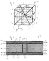
Figur 1- eine Leiterbahnstruktur eines Metamaterials;
Figur 2- einen Schnitt durch ein planares Metamaterial, das eine in einem Schichtenstapel angeordnete Leiterbahnstruktur aufweist, die zu der Leiterbahnstruktur des Metamaterials aus
Figur 1 Figur 3- eine Aufsicht auf einzelne Schichten des Schichtenstapels aus
Figur 2 Figur 4- eine Aufsicht auf eine Grundschicht vier benachbarter Basiszellen des Schichtenstapels aus
Figur 2 Figur 5- eine Aufsicht auf eine Koppelschicht vier benachbarter Basiszellen des Schichtenstapels aus
Figur 2 Figur 6- eine Aufsicht auf einzelne Schichten der Schichtenfolge eines abgewandelten planaren Metamaterials mit Schichtstruktur;
Figur 7- eine Aufsicht auf eine Grundschicht des Metamaterials aus
Figur 6 Figur 8- ein Diagramm mit der Dispersionsrelation eines Metamaterials gemäß den
Figuren 2 bis 5 Figur 9- eine Teilansicht auf die Leiterbahnstruktur einer dreidimensionalen Basiszelle eines weiteren Metamaterials;
Figur 10- eine Aufsicht auf einzelne Schichten der Schichtenfolge eines Metamaterials, dessen Leiterbahnstruktur elektrisch äquivalent zu der Leiterbahnstruktur des Metamaterials aus
Figur 9 ist; und Figur 11- eine Aufsicht auf einzelne Schichten der Schichtenfolge eines weiteren Metamaterials, dessen Leiterbahnstruktur zu der Leiterbahnstruktur des Metamaterials aus
Figur 9 elektrisch äquivalent ist.
- FIG. 1
- a trace structure of a metamaterial;
- FIG. 2
- a section through a planar metamaterial having a arranged in a stack of layers track structure, which is to the track structure of the metamaterials
FIG. 1 is electrically equivalent; - FIG. 3
- a view of individual layers of the layer stack
FIG. 2 ; - FIG. 4
- a plan view of a base layer of four adjacent basic cells of the layer stack from
FIG. 2 ; - FIG. 5
- a plan view of a coupling layer of four adjacent basic cells of the layer stack
FIG. 2 ; - FIG. 6
- a plan view of individual layers of the layer sequence of a modified planar metamaterial having a layer structure;
- FIG. 7
- a top view of a base layer of the metamaterials
FIG. 6 ; - FIG. 8
- a diagram with the dispersion relation of a metamaterials according to the
FIGS. 2 to 5 ; - FIG. 9
- a partial view of the wiring structure of a three-dimensional basic cell of another metamaterials;
- FIG. 10
- a plan view of individual layers of the layer sequence of a metamaterials, its interconnect structure electrically equivalent to the interconnect structure of the metamaterials
FIG. 9 is; and - FIG. 11
- a plan view of individual layers of the layer sequence of a further metamaterials, whose conductor structure to the conductor track structure of the metamaterials
FIG. 9 is electrically equivalent.
Durch eine Vielzahl von nebeneinander und gegebenenfalls auch übereinander angeordneten Basiszellen von der Art der Basiszelle 1 ergibt sich ein Metamaterial, das in einem bestimmten Frequenzbereich einen negativen Brechungsindex oder einen Brechungsindex kleiner 1 aufweist. Allerdings ist die Herstellung des Metamaterials in der Praxis nicht einfach, da eine sehr große Zahl der Basiszellen 1 hergestellt und untereinander verbunden werden muss. Typischerweise müssen für praktische Anwendungen Metamaterialien hergestellt werden, bei denen die Anzahl von Basiszellen 1 in der Größenordnung 105 liegen.By a plurality of side by side and optionally also superimposed basic cells of the type of
Die Metallisierungsschichten 10 können durch die üblichen Verfahren der Halbleiter- und Mikrosystemtechnik auf die dielektrischen Lagen 9 aufgebracht und dort strukturiert werden. Außerdem können die Metallisierungsschichten 10 über die dielektrischen Lagen 9 hinweg mithilfe von Durchkontaktierung 16 verbunden werden.The metallization layers 10 can be applied to the
Die Basiszelle 8 ist zu der Basiszelle 1 aus
Durch die Koppelschichten 11 und 15 werden auch übereinander gestapelte Basiszellen 8 miteinander verkoppelt. Beispielsweise verkoppelt die Kapazitätsfläche 17 mit der Bezeichnung P1A kapazitiv die über der Kapazitätsfläche 17 liegende Kapazitätsfläche 19 mit der Bezeichnung P2A mit der darunter liegenden Kapazitätsfläche 19 mit der Bezeichnung P4A der darunter liegenden Basiszelle 8.Through the coupling layers 11 and 15 and stacked
Die Metallisierungen in der unteren Koppelschicht 11 und der unteren Koppelschicht 15 sind identisch, wobei die obere Koppelschicht 15 einer unten liegenden Basiszelle 8 gleich der unteren Koppelschicht 11 einer oben liegenden Basiszelle 8 ist. Es ist daher nur notwendig, in jeder Basiszelle 8 entweder die untere Koppelschicht 11 oder die obere Koppelschicht 15 auszubilden.The metallizations in the
In
In
In
Für die Simulation wurde a = 20 mm und h1 = 5 mm, h2 = 1 mm, ε1 = 1 und ε2 = 10 gewählt. Für die Simulation wurden zwei verschiedene Simulationsprogramme verwendet, deren Ergebnisse jeweils mit gestrichelten Linien und durchgezogenen Linien in das Diagramm in
Es sei angemerkt, dass die einander gegenüberliegende Kapazitätsflächen 32 in einem Abstand 35 angeordnet sind. Ferner sind die Kapazitätsflächen 32 entlang den Kanten der Pyramide 34 beabstandet.It should be noted that the opposing capacity surfaces 32 are arranged at a
In
In der darüberliegenden Grundschicht 12 sind die Durchkontaktierungen 40 an jeweils zwei schwalbenschwanzförmige Kapazitätsflächen 42 angeschlossen. Die Kapazitätsflächen 42 sind dabei jeweils mit der konvexen Innenseite einander zugewandt angeordnet. Außerdem verläuft die konvexe Innenseite der Kapazitätsflächen 42 jeweils entlang der Diagonalen der Basiszelle 36.In the
Die Kapazitätsflächen 42 decken oder überlagern sich mit Kapazitätsflächen 43, die in der Zwischenschicht 13 ausgebildet sind. Die bei der Basiszelle 36 gemäß
Die Kapazitätsflächen 45 sind schließlich über die Durchkontaktierungen 41 mit einer in
Bei der Basiszelle 36 gemäß
Es sei angemerkt, dass die Basiszelle 47 in
Ferner sei angemerkt, dass durch die Basiszellen 36 und 47 die Basiszelle 28, die die Punktsymmetriegruppe Th hat, in eine planare Leiterbahnstruktur mit der Punktsymmetriegruppe S2 abgebildet wird.It should also be noted that the base cell 28, which has the point symmetry group T h , is mapped into a planar printed conductor structure having the point symmetry group S 2 by the
Die hier beschriebenen Basiszellen eignen sich für die Massenfertigung mithilfe üblicher Verfahren der Halbleiter- und Mikrosystemtechniken, so dass sich die Metamaterialien mit den hier beschriebenen Basiszellen im industriellen Maßstab fertigen lassen.The basic cells described herein are suitable for mass production by conventional methods of semiconductor and microsystem techniques, so that the metamaterials with the basic cells described herein can be manufactured on an industrial scale.
Es sei angemerkt, dass sich mit den Basiszellen 8, 22, 36 und 47 ein Metamaterial herstellen lässt, das auch in Wellenausbreitungsrichtungen, die keinen rechten Winkel zur Stapelrichtung einnehmen und somit außerhalb der Schichtebene liegen, in einem bestimmten Frequenzbereich ein Verhalten als Metamaterial, insbesondere ein Verhalten eines Metamaterial mit negativen Brechungsindex zeigt. Insofern weist ein Metamaterial mit den Basiszellen 8, 22, 36 und 47 ein ähnliches Transmissionsverhalten wie ein Metamaterial auf, das aus den Basiszellen 1 und 28 zusammengesetzt ist und das in jede Wellenausbreitungsrichtung in einem bestimmten Frequenzbereich ein für ein Metamaterial typisches Transmissionsverhalten zeigt.It should be noted that it is possible with the
Die Leiterbahnstruktur des jeweiligen Metamaterials ist dabei vorzugsweise so ausgebildet, dass sich die Basiszellen 8, 22, 36 oder 47 in alle drei Raumrichtungen wiederholen.The interconnect structure of the respective metamaterial is preferably designed such that the
Abschließend sei noch darauf hingewiesen, dass Merkmale und Eigenschaften, die im Zusammenhang mit einem bestimmten Ausführungsbeispiel beschrieben worden sind, auch mit einem anderen Ausführungsbeispiel kombiniert werden können, außer wenn dies aus Gründen der Kompatibilität ausgeschlossen ist.Finally, it should be noted that features and properties that have been described in connection with a particular embodiment can also be combined with another embodiment, except where this is excluded for reasons of compatibility.
Schließlich wird noch darauf hingewiesen, dass in den Ansprüchen und in der Beschreibung der Singular den Plural einschließt, außer wenn sich aus dem Zusammenhang etwas anderes ergibt. Insbesondere wenn der unbestimmte Artikel verwendet wird, ist sowohl der Singular als auch der Plural gemeint.Finally, it should be noted that in the claims and in the description, the singular includes the plural unless the context indicates otherwise. In particular, when the indefinite article is used, it means both the singular and the plural.
Claims (12)
dadurch gekennzeichnet, dass die Leiterbahnstruktur der Basiszelle (8, 22, 36, 47) auf wenigsten drei in einem Stapel übereinander angeordnete Leiterbahnschichten (11-15, 48, 49) verteilt ist.Metamaterial comprising a plurality of repetitive basic cells (8, 22, 36, 47), each having a three-dimensional trace structure that exhibits the transmission characteristic characteristic of the metamaterial for electromagnetic waves having wave propagation directions in three spatial dimensions;
characterized in that the conductor track structure of the base cell (8, 22, 36, 47) on at least three in a stack stacked conductor track layers (11-15, 48, 49) is distributed.
dadurch gekennzeichnet, dass sich die Schichtenfolge einer Basiszelle (8, 22, 36, 47) in Stapelrichtung periodisch wiederholt.Metamaterial according to claim 1,
characterized in that the layer sequence of a basic cell (8, 22, 36, 47) repeats periodically in the stacking direction.
dadurch gekennzeichnet, dass zwischen den Leiterbahnschichten (11-15, 48, 49) dielektrische Abstandsschichten (9) angeordnet sind.Metamaterial according to claim 1 or 2,
characterized in that between the conductor track layers (11-15, 48, 49) dielectric spacer layers (9) are arranged.
dadurch gekennzeichnet, dass die dielektrische Abstandsschicht (9) den Raum zwischen den Leiterbahnschichten (11-15, 48, 49) füllt.Metamaterial according to claim 3,
characterized in that the dielectric spacer layer (9) fills the space between the wiring layers (11-15, 48, 49).
dadurch gekennzeichnet, dass die Leiterbahnstruktur die Punktsymmetriegruppe D4h aufweist.Metamaterial according to claims 1 to 4,
characterized in that the conductor track structure has the point symmetry group D 4h .
dadurch gekennzeichnet, dass die Basiszelle (8, 22) eine Grundschicht (12), eine Zwischenschicht (13) und eine Deckschicht (14) aufweist, und dass in der Grundschicht (12) und in der Deckschicht (14) in den Ecken (18) der Basiszelle (8, 28) jeweils Kapazitätsflächen (19, 23) angeordnet sind, die über induktive Komponenten (16, 20) mit einem gemeinsamen Knotenpunkt (21) in der Zwischenschicht (13) verbunden sind.Metamaterial according to one of claims 1 to 5,
characterized in that the base cell (8, 22) has a base layer (12), an intermediate layer (13) and a cover layer (14), and that in the base layer (12) and in the cover layer (14) in the Cores (18) of the base cell (8, 28) are each arranged capacitance surfaces (19, 23) which are connected via inductive components (16, 20) to a common node (21) in the intermediate layer (13).
dadurch gekennzeichnet, dass benachbarte Basiszellen (22) durch eine außenseitig an den Kapazitätsflächen (23) ausgebildete Interdigitalstruktur (24) kapazitiv gekoppelt sind.Metamaterial according to claim 6,
characterized in that adjacent basic cells (22) are capacitively coupled by an interdigital structure (24) formed on the outside of the capacitance surfaces (23).
dadurch gekennzeichnet, dass zwischen der Grundschicht (12) und der Deckschicht (14) von in Stapelrichtung übereinander angeordneten Basiszellen (8) jeweils eine Koppelschicht (11, 15) ausgebildet ist, in der sich über mehrere Basiszellen (8) erstreckende Kapazitätsflächen (17) ausgebildet sind, durch die die Kapazitätsflächen (19) in der Grundschicht (12) und der Deckschicht (15) von benachbarten Basiszellen (8) kapazitiv gekoppelt sind.Metamaterial according to claim 6,
characterized in that in each case a coupling layer (11, 15) is formed between the base layer (12) and the cover layer (14) of stacked base cells (8), in which capacitive surfaces (17) extending over a plurality of base cells (8) are formed. are formed, through which the capacitance surfaces (19) in the base layer (12) and the cover layer (15) of adjacent base cells (8) are capacitively coupled.
dadurch gekennzeichnet, dass die Leiterbahnstruktur die Punktsymmetriegruppe S2 aufweist.Metamaterial according to one of claims 1 to 4,
characterized in that the conductor track structure has the point symmetry group S 2 .
dadurch gekennzeichnet, dass die Basiszelle (36, 47) eine Grundschicht (12), eine Zwischenschicht (13) und eine Deckschicht (14) aufweist, wobei in der Zwischenschicht (13) zwei Kapazitätsflächen (43) ausgebildet sind, die über eine induktive Leiterbahn (44) verbunden sind und in der Grundschicht (12) und der Deckschicht (14) mit den Kapazitätsflächen (43) in der Zwischenschicht (13) kapazitiv gekoppelte Kapazitätsflächen (42, 45) ausgebildet sind, die jeweils Durchkontaktierungen (40, 41) zu Koppelflächen (11, 15) aufweisen, die der dielektrischen Verbindung der Basiszelle (36, 47) mit benachbarten Basiszellen (36, 47) dienen.Metamaterial according to claim 9,
characterized in that the base cell (36, 47) has a base layer (12), an intermediate layer (13) and a cover layer (14), wherein in the intermediate layer (13) two capacitance surfaces (43) are formed, which via an inductive conductor track (44) are connected and in the base layer (12) and the cover layer (14) with the capacitive surfaces (43) in the intermediate layer (13) capacitively coupled capacitance surfaces (42, 45) are formed, the respective vias (40, 41) Coupling surfaces (11, 15), the dielectric Connecting the base cell (36, 47) serve with adjacent base cells (36, 47).
dadurch gekennzeichnet, dass die Koppelschicht mit den Durchführungen (40, 41) über Interdigitalstrukturen (39) kapazitiv gekoppelte Kapazitätsflächen (37) verfügt, die über eine mittlere Interdigitalstruktur (38) zu Paaren verbunden sind und an die induktive Leitungen (46) angeschlossen sind, die dazu dienen, benachbarte Basiszellen (36) zu verbinden.Metamaterial according to claim 10,
characterized in that the coupling layer with the feedthroughs (40, 41) has capacitively coupled capacitance surfaces (37) via interdigital structures (39), which are connected in pairs via a central interdigital structure (38) and to which the inductive lines (46) are connected, which serve to connect adjacent basic cells (36).
dadurch gekennzeichnet, dass die Koppelschichten eine äußere Koppelschicht (48) und eine innere Koppelschicht (49) aufweisen, wobei auf der inneren Koppelschicht (48) an die Durchführungen (40, 41) angeschlossene Kapazitätsflächen (50) ausgebildet sind, die jeweils mit einem Paar von Kapazitätsflächen (37) auf der äußeren Koppelschicht (48) gekoppelt sind, wobei die Kapazitätsflächen (37) auf der äußeren Koppelschicht (48) an induktive Leitungen (46) angeschlossen sind, die der elektrischen Verbindung benachbarter Basiszellen (47) dienen.Metamaterial according to claim 10,
characterized in that the coupling layers have an outer coupling layer (48) and an inner coupling layer (49), wherein on the inner coupling layer (48) to the bushings (40, 41) connected capacitance surfaces (50) are formed, each with a pair capacitive surfaces (37) are coupled to the outer coupling layer (48), wherein the capacitive surfaces (37) on the outer coupling layer (48) to inductive lines (46) are connected, which serve the electrical connection of adjacent base cells (47).
Applications Claiming Priority (1)
| Application Number | Priority Date | Filing Date | Title |
|---|---|---|---|
| DE102007029691 | 2007-06-27 |
Publications (1)
| Publication Number | Publication Date |
|---|---|
| EP2009740A1 true EP2009740A1 (en) | 2008-12-31 |
Family
ID=39760897
Family Applications (1)
| Application Number | Title | Priority Date | Filing Date |
|---|---|---|---|
| EP08159291A Withdrawn EP2009740A1 (en) | 2007-06-27 | 2008-06-27 | Metamaterial |
Country Status (1)
| Country | Link |
|---|---|
| EP (1) | EP2009740A1 (en) |
Cited By (1)
| Publication number | Priority date | Publication date | Assignee | Title |
|---|---|---|---|---|
| CN110690576A (en) * | 2019-09-03 | 2020-01-14 | 北京航空航天大学青岛研究院 | Device and method for realizing electromagnetic wave modulation based on metamaterial three-dimensional structure |
Citations (4)
| Publication number | Priority date | Publication date | Assignee | Title |
|---|---|---|---|---|
| WO2004025783A1 (en) * | 2002-09-14 | 2004-03-25 | Bae Systems Plc | Periodic electromagnetic structure |
| WO2006023195A2 (en) * | 2004-07-23 | 2006-03-02 | The Regents Of The University Of California | Metamaterials |
| US20060243925A1 (en) * | 2005-05-02 | 2006-11-02 | Raytheon Company | Smith-Purcell radiation source using negative-index metamaterial (NIM) |
| WO2007073716A1 (en) | 2005-12-13 | 2007-07-05 | Technische Universität München | Base unit and device for the transfer of electromagnetic fields |
-
2008
- 2008-06-27 EP EP08159291A patent/EP2009740A1/en not_active Withdrawn
Patent Citations (4)
| Publication number | Priority date | Publication date | Assignee | Title |
|---|---|---|---|---|
| WO2004025783A1 (en) * | 2002-09-14 | 2004-03-25 | Bae Systems Plc | Periodic electromagnetic structure |
| WO2006023195A2 (en) * | 2004-07-23 | 2006-03-02 | The Regents Of The University Of California | Metamaterials |
| US20060243925A1 (en) * | 2005-05-02 | 2006-11-02 | Raytheon Company | Smith-Purcell radiation source using negative-index metamaterial (NIM) |
| WO2007073716A1 (en) | 2005-12-13 | 2007-07-05 | Technische Universität München | Base unit and device for the transfer of electromagnetic fields |
Non-Patent Citations (4)
| Title |
|---|
| GRBIC ANTHONY ET AL: "An isotropic three-dimensional negative-refractive-index transmission-line metamaterial", JOURNAL OF APPLIED PHYSICS, AMERICAN INSTITUTE OF PHYSICS. NEW YORK, US, vol. 98, no. 4, 22 August 2005 (2005-08-22), pages 43106 - 043106, XP012078340, ISSN: 0021-8979 * |
| HOEFER W ET AL: "Topology and Design of Wide-Band 3D Metamaterials Made of Periodically Loaded Transmission Line Arrays", MICROWAVE SYMPOSIUM DIGEST, 2005 IEEE MTT-S INTERNATIONAL LONG BEACH, CA, USA 12-17 JUNE 2005, PISCATAWAY, NJ, USA,IEEE, 12 June 2005 (2005-06-12), pages 313 - 316, XP010844474, ISBN: 978-0-7803-8846-8 * |
| IYER, A. K.; ELEFTHE-RIADES, G. V.: "Volumetric layered transmission-line metamaterial exhibiting a negative refractive index", J. OPT. SOC. AM. B, vol. 23, no. 3, March 2006 (2006-03-01), pages 553 - 580, XP055128363, DOI: doi:10.1364/JOSAB.23.000553 |
| LAI, A.; ITOH, T.: "Composite right/left-handed transmission line metamaterials", IEEE, MICROWAVE MAGAZIN, September 2004 (2004-09-01), pages 34 - 50, XP011119759 |
Cited By (1)
| Publication number | Priority date | Publication date | Assignee | Title |
|---|---|---|---|---|
| CN110690576A (en) * | 2019-09-03 | 2020-01-14 | 北京航空航天大学青岛研究院 | Device and method for realizing electromagnetic wave modulation based on metamaterial three-dimensional structure |
Similar Documents
| Publication | Publication Date | Title |
|---|---|---|
| EP2143117B1 (en) | Electric multi-layer component with electrically non-contacted protective structure | |
| DE4008507C2 (en) | Laminated LC filter | |
| DE60114200T2 (en) | CERAMIC MULTILAYER CONDENSER NETWORK | |
| DE2714426C3 (en) | Passive circuit element designed as a low-pass element or as a delay element | |
| DE4317545A1 (en) | Thin film transformer | |
| DE102009028629A9 (en) | Ultra-broadband capacitor | |
| DE2045560A1 (en) | Rectangular waveguide resonator and microwave filter built with such resonators | |
| DE3425232A1 (en) | MULTILAYER CERAMIC CAPACITOR | |
| DE4021634A1 (en) | NOISE FILTER | |
| DE3144026A1 (en) | "TRANSFORMER" | |
| DE1940036C3 (en) | Capacitive network with frontal contact | |
| DE102010021164A1 (en) | Balanced / Unbalanced working SAW filter | |
| DE10212868A1 (en) | Semiconductor device and method for its manufacture | |
| EP2009740A1 (en) | Metamaterial | |
| DE3142949A1 (en) | JOSEPHSON ELEMENT AND METHOD FOR THE PRODUCTION THEREOF | |
| WO2006015581A2 (en) | Piezoelectric transformer | |
| DE102005045638B4 (en) | With surface waves working transducer | |
| DE202008006222U1 (en) | metamaterial | |
| DE112018005526B4 (en) | Acoustic wave device and method of manufacturing an acoustic wave device | |
| DE112020006270T5 (en) | FREQUENCY-SELECTIVE SURFACE ELEMENT, FREQUENCY-SELECTIVE SURFACE AND ELECTROMAGNETIC WAVE ABSORBER | |
| EP2054953B1 (en) | Piezoelectric transformer | |
| DE3731165C2 (en) | ||
| DE4234486C1 (en) | Arrangement for splitting an optical input signal into two signals with mutually orthogonal polarization | |
| EP2465123B1 (en) | Electrical multilayer component | |
| DE4410753C2 (en) | Capacitor array |
Legal Events
| Date | Code | Title | Description |
|---|---|---|---|
| PUAI | Public reference made under article 153(3) epc to a published international application that has entered the european phase |
Free format text: ORIGINAL CODE: 0009012 |
|
| AK | Designated contracting states |
Kind code of ref document: A1 Designated state(s): AT BE BG CH CY CZ DE DK EE ES FI FR GB GR HR HU IE IS IT LI LT LU LV MC MT NL NO PL PT RO SE SI SK TR |
|
| AX | Request for extension of the european patent |
Extension state: AL BA MK RS |
|
| 17P | Request for examination filed |
Effective date: 20090427 |
|
| 17Q | First examination report despatched |
Effective date: 20090602 |
|
| AKX | Designation fees paid |
Designated state(s): AT BE BG CH CY CZ DE DK EE ES FI FR GB GR HR HU IE IS IT LI LT LU LV MC MT NL NO PL PT RO SE SI SK TR |
|
| STAA | Information on the status of an ep patent application or granted ep patent |
Free format text: STATUS: THE APPLICATION IS DEEMED TO BE WITHDRAWN |
|
| 18D | Application deemed to be withdrawn |
Effective date: 20120103 |