EP2009679A1 - Semiconductor device - Google Patents
Semiconductor device Download PDFInfo
- Publication number
- EP2009679A1 EP2009679A1 EP07012358A EP07012358A EP2009679A1 EP 2009679 A1 EP2009679 A1 EP 2009679A1 EP 07012358 A EP07012358 A EP 07012358A EP 07012358 A EP07012358 A EP 07012358A EP 2009679 A1 EP2009679 A1 EP 2009679A1
- Authority
- EP
- European Patent Office
- Prior art keywords
- substrate
- modified regions
- semiconductor device
- locally modified
- semiconductor
- Prior art date
- Legal status (The legal status is an assumption and is not a legal conclusion. Google has not performed a legal analysis and makes no representation as to the accuracy of the status listed.)
- Withdrawn
Links
Images

Classifications
-
- H—ELECTRICITY
- H01—ELECTRIC ELEMENTS
- H01L—SEMICONDUCTOR DEVICES NOT COVERED BY CLASS H10
- H01L21/00—Processes or apparatus adapted for the manufacture or treatment of semiconductor or solid state devices or of parts thereof
- H01L21/02—Manufacture or treatment of semiconductor devices or of parts thereof
- H01L21/027—Making masks on semiconductor bodies for further photolithographic processing not provided for in group H01L21/18 or H01L21/34
- H01L21/033—Making masks on semiconductor bodies for further photolithographic processing not provided for in group H01L21/18 or H01L21/34 comprising inorganic layers
- H01L21/0334—Making masks on semiconductor bodies for further photolithographic processing not provided for in group H01L21/18 or H01L21/34 comprising inorganic layers characterised by their size, orientation, disposition, behaviour, shape, in horizontal or vertical plane
- H01L21/0337—Making masks on semiconductor bodies for further photolithographic processing not provided for in group H01L21/18 or H01L21/34 comprising inorganic layers characterised by their size, orientation, disposition, behaviour, shape, in horizontal or vertical plane characterised by the process involved to create the mask, e.g. lift-off masks, sidewalls, or to modify the mask, e.g. pre-treatment, post-treatment
-
- H—ELECTRICITY
- H01—ELECTRIC ELEMENTS
- H01L—SEMICONDUCTOR DEVICES NOT COVERED BY CLASS H10
- H01L21/00—Processes or apparatus adapted for the manufacture or treatment of semiconductor or solid state devices or of parts thereof
- H01L21/02—Manufacture or treatment of semiconductor devices or of parts thereof
- H01L21/04—Manufacture or treatment of semiconductor devices or of parts thereof the devices having potential barriers, e.g. a PN junction, depletion layer or carrier concentration layer
- H01L21/18—Manufacture or treatment of semiconductor devices or of parts thereof the devices having potential barriers, e.g. a PN junction, depletion layer or carrier concentration layer the devices having semiconductor bodies comprising elements of Group IV of the Periodic Table or AIIIBV compounds with or without impurities, e.g. doping materials
- H01L21/26—Bombardment with radiation
- H01L21/263—Bombardment with radiation with high-energy radiation
- H01L21/265—Bombardment with radiation with high-energy radiation producing ion implantation
- H01L21/26506—Bombardment with radiation with high-energy radiation producing ion implantation in group IV semiconductors
-
- H—ELECTRICITY
- H10—SEMICONDUCTOR DEVICES; ELECTRIC SOLID-STATE DEVICES NOT OTHERWISE PROVIDED FOR
- H10D—INORGANIC ELECTRIC SEMICONDUCTOR DEVICES
- H10D30/00—Field-effect transistors [FET]
- H10D30/01—Manufacture or treatment
- H10D30/021—Manufacture or treatment of FETs having insulated gates [IGFET]
- H10D30/024—Manufacture or treatment of FETs having insulated gates [IGFET] of fin field-effect transistors [FinFET]
-
- H—ELECTRICITY
- H10—SEMICONDUCTOR DEVICES; ELECTRIC SOLID-STATE DEVICES NOT OTHERWISE PROVIDED FOR
- H10D—INORGANIC ELECTRIC SEMICONDUCTOR DEVICES
- H10D30/00—Field-effect transistors [FET]
- H10D30/60—Insulated-gate field-effect transistors [IGFET]
- H10D30/62—Fin field-effect transistors [FinFET]
Definitions
- the present invention relates to a method for forming a semiconductor device on a substrate, e.g. a bulk semiconductor substrate or a semiconductor-on-insulator substrate, and to a semiconductor device thus obtained.
- the semiconductor device obtained with a method according to the present invention comprises locally modified regions with increased etching resistance. This leads to semiconductor devices with improved properties such as good electrical properties and good mechanical stability.
- Silicon on insulator (SOI) technology refers to the use of a layered silicon-insulator-silicon substrate in semiconductor manufacturing, especially microelectronics.
- SOI substrates comprise a thin, insulating layer, such as silicon oxide or glass, between a thin layer of silicon and a silicon bulk substrate.
- SOI-based devices thus differ from conventional silicon-built devices in that the silicon junction is above an electrical insulator, typically silicon dioxide.
- a FinFET fin field-effect transistor
- a FinFET comprises a thin silicon (Si) fin with a gate running over the fin.
- the gate controls a channel at least along the sidewalls of the fin.
- the electrical width of the channel is defined by the geometrical dimensions of the fin, particularly by the height and the width of the fin.
- a distinguishing characteristic of a FinFET with respect to other semiconductor devices is that a conducting gate is wrapped around the thin Si fin which forms the body of the device.
- the use of SOI substrates with a silicon layer on a buried oxide (BOX) may, after patterning of the silicon layer of the SOI substrate, lead to formation of recesses in the BOX and under-etch regions in the BOX under the patterned silicon layer.
- BOX recesses and under-etch regions may be formed during further processing of the FinFET, for example during removal of a hardmask used to pattern the silicon layer.
- Residues of materials used during further processing of the FinFET may stick in these BOX recesses and especially in the under-etch regions.
- An additional process step may then be necessary to remove these residues.
- the residues may be difficult to remove and may thus still be present in the final FinFET. This may have an impact on the electrical properties of the device formed on the substrates, may degrade the mechanical stability of the FinFET and may degrade the device matching, yield, etc.
- any semiconductor device formed on a substrate e.g. bulk semiconductor substrate or semiconductor-on-insulator substrate, lying in a plane, in which the semiconductor device is formed of a structure extending from the substrate in a direction substantially perpendicular to the plane of the substrate.
- Semiconductor devices obtained by the method according to embodiments of the invention may have improved properties such as improved electrical properties and improved mechanical stability.
- a method for forming a semiconductor device on a substrate having a first major surface lying in a plane comprises:
- etching resistance With increasing etching resistance is meant that the locally modified regions have a reduced etching speed compared to the original, non-modified substrate. Locally increasing etching resistance may prevent under-etching of the at least one structure during further process steps in the formation of the semiconductor device.
- the method according to embodiments of the invention may lead to semiconductor devices with good electrical properties and good mechanical stability.
- the substrate may be a semiconductor-on-insulator substrate, such as a silicon-on-insulator (SOI) substrate, a germanium-on-insulator (GOI) substrate or a silicon-germanium-on-insulator (SGOI) substrate.
- SOI silicon-on-insulator
- GOI germanium-on-insulator
- SGOI silicon-germanium-on-insulator
- the invention may provide a method for forming a semiconductor device on a semiconductor-on-insulator substrate comprising a semiconductor layer on an insulating layer having a surface. The method may comprise:
- the insulating layer may be a buried oxide.
- the substrate may be a bulk semiconductor substrate having a major surface lying in a plane, and the method may comprise:
- the substrate may have a major surface lying in a plane. Forming locally modified regions in the substrate may be performed by implanting implantation elements, also called species or implantation species, in a direction substantially perpendicular to the plane of the major surface of the substrate.
- implanting implantation elements also called species or implantation species
- implantation elements also called species or implantation species
- substantially perpendicular elements suitable to be implanted into a semiconductor or insulating layer.
- substantially perpendicular is meant that the direction of implantation of the implantation elements may most preferably make an angle of between 0 and 5 degrees with a direction substantially perpendicular to the plane of the major surface of the substrate such that substantially no implantation elements can enter the at least one structure through its sidewalls.
- substantially no implantation elements entering the at least one structure is meant that a concentration of preferably less than 1 E12 cm -2 and more preferably less than 1 E10 cm -2 of implantation elements may enter the at least one structure during implantation of implantation elements to form the locally modified regions.
- An advantage hereof is that implantation elements are not implanted in sidewalls of parts of the semiconductor device formed on the substrate. For example, in case of a FinFET, implantation elements are not implanted in sidewalls of the fin.
- Implanting implantation elements may, according to embodiments, be performed by ion implantation.
- implanting implantation elements may be performed by plasma doping.
- An advantage of plasma doping or PLAD is that this technique allows implantation of implantation elements in a direction substantially perpendicular to the plane of the major surface of the substrate, i.e. at an incidence angle of substantially zero degrees with a direction substantially perpendicular to the plane of the major surface of the substrate.
- PLAD furthermore allows implantation of high doses of implantation elements of 1E13 to 1E17 cm -2 such that a peak of implantation elements is located at the surface of the substrate not covered by the at least one structure.
- the implantation elements may comprise carbon, nitrogen, oxygen or a combination thereof.
- the method may furthermore comprise extending the locally modified regions under the at least one structure.
- Extending the locally modified regions under the at least one structure may be performed by annealing.
- Annealing may be performed at a temperature of between 800°C and 1000°.
- Annealing may be performed during a time period of between 1 second and 60 seconds.
- Annealing may lead to formation of locally modified regions with a thickness of between 1 nm and 20 nm.
- patterning the substrate may be performed by:
- Providing a mask may comprise providing a hardmask comprising at least one of a metal, a nitride, an oxide or a low-k material.
- providing a mask may comprise providing a photoresist polymer.
- a semiconductor device comprising at least one structure extending from a substrate having a major surface lying in a plane, the structure extending in a direction substantially perpendicular to the plane of the major surface of the substrate, wherein the semiconductor device furthermore comprises locally modified regions in the substrate at locations not covered by the at least one structure, the locally modified regions having an increased etch resistance with respect to the etch resistance of the non-modified substrate.
- the semiconductor devices according to embodiments of the invention have good electrical properties and good mechanical stability.
- the substrate may be a semiconductor-on-insulator substrate, such as a silicon-on-insulator (SOI) substrate, a germanium-on-insulator (GOI) substrate or a silicon-germanium-on-insulator (SGOI) substrate.
- the invention may provide a semiconductor device comprising at least one structure formed of a patterned semiconductor layer on an insulating layer of the semiconductor-on-insulator substrate, the insulating layer having a surface and the semiconductor device furthermore comprising locally modified regions in the insulating layer at locations which are not covered by the patterned semiconductor layer.
- the locally modified regions may have an increased etching resistance compared to the original, non-modified substrate.
- the insulating layer may be a buried oxide.
- the substrate may be a bulk semiconductor substrate.
- the bulk semiconductor substrate may be any of a bulk silicon substrate, a bulk Ge substrate, a bulk GaAs substrate, a bulk GaN substrate.
- the locally modified regions may be regions implanted with carbon, nitrogen, oxygen or a combination thereof.
- the locally modified regions may have a concentration of implantation elements, e.g. a carbon, nitrogen or oxygen concentration of between 1E13 cm -2 and 1E17 cm -2 .
- the locally modified regions may have a thickness of between 1 nm and 20 nm.
- the locally modified regions may extend underneath the at least one structure.
- the semiconductor device may be a FinFET.
- An advantage of the device according to embodiments of the present invention is that by providing locally modified regions in a substrate or part of a substrate, e.g. a buried oxide (BOX) of an SOI (silicon-on-insulator) substrate or part of a bulk semiconductor substrate, at locations which are not covered by a part of the semiconductor device, the substrate or part of the substrate is protected during further processing of the semiconductor device such that formation of recesses and under-etched regions in the substrate or part of the substrate may be prevented.
- a substrate or part of a substrate e.g. a buried oxide (BOX) of an SOI (silicon-on-insulator) substrate or part of a bulk semiconductor substrate
- the device obtained by the method according to embodiments of the present invention may have good electrical properties and a good mechanical stability.
- transistors These are three-terminal devices having a first main electrode such as a drain, a second main electrode such as a source and a control electrode such as a gate for controlling the flow of electrical charges between the first and second main electrodes. It will be clear for a person skilled in the art that the present invention is also applicable to similar devices that can be configured in any transistor technology, including for example, but not limited thereto, CMOS, BICMOS and Bipolar technology.
- the present invention provides a method for forming a semiconductor device on a substrate having a first major surface lying in a plane .
- the method comprises:
- a device obtained by a method according to embodiments of the present invention may have good electrical properties and a good mechanical stability.
- the method according to embodiments of the invention may advantageously be used in the formation of a semiconductor device, e.g. a finFET, on a semiconductor-on-insulator substrate for protecting the insulating layer of the semiconductor-on-insulator substrate by preventing under-etching of the at least one structure formed on the substrate during further process steps in the formation of the semiconductor device.
- the method may also be advantageously used in the formation of a semiconductor device, e.g. a finFET, on a bulk semiconductor substrate for protecting part of the semiconductor substrate not covered by the at least one structure by preventing under-etching of the at least one structure formed on the substrate during further process steps in the formation of the semiconductor device.
- the substrate may be a semiconductor-on-insulator substrate comprising a semiconductor layer on an insulating layer.
- the substrate may, for example, be a silicon-on-insulator (SOI) substrate, a germanium-on-insulator (GOI) substrate or a silicon-germanium-on-insulator (SGOI) substrate.
- SOI silicon-on-insulator
- GOI germanium-on-insulator
- SGOI silicon-germanium-on-insulator
- a method may be provided for forming a semiconductor device on a semiconductor-on-insulator substrate, the semiconductor-on-insulator substrate comprising a semiconductor layer, e.g. silicon layer, on an insulating layer, e.g. a buried oxide, having a surface.
- the method according to these embodiments may comprise:
- An advantage of the method according to the first embodiment of the present invention is that by providing locally modified regions in the insulating layer, e.g. buried oxide (BOX), of the semiconductor-on-insulator substrate at locations which are not covered by a part of the semiconductor device, the insulating layer, e.g. buried oxide, is protected during further processing of the semiconductor device such that formation of recesses and under-etched regions in the insulating layer may be prevented.
- the insulating layer e.g. buried oxide (BOX)
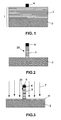
- Fig. 1 to Fig. 6 illustrate subsequent steps in a method for manufacturing a FinFET 10 according to embodiments of the invention.
- an SOI substrate 1 comprising a bulk substrate (not shown in the figures), an insulating layer such as a buried oxide 2 and a silicon layer 3 is provided.
- the buried oxide 2 may typically have a thickness of between 50 nm and 200 nm and may, for example, be 150 nm.
- the buried oxide 2 may preferably comprise SiO 2 .
- the silicon layer 3 may typically have a thickness of between 10 nm and 100 nm and may, for example, be 65 nm.
- the silicon layer 3, of which an upper surface (surface away from the buried oxide 2) forms a major surface of the SOI substrate 1, is patterned so as, to form at least one structure 20, in the example given at least one fin (see further), extending from the substrate 1 in, when the major surface of the substrate 1 is lying in a plane, a direction substantially perpendicular to the plane of the major surface of the substrate 1.
- the substrate 1 may comprise any number of structures 20 required to form a particular semiconductor device 10.
- Patterning of the silicon layer 3 may be hardmask-based or may be done by photolithography using a photoresist.
- a hardmask layer may be provided on the silicon layer 3.
- the hardmask layer may have a thickness of between 50 nm and 100 nm and may, for example, be 70 nm.
- the hardmask layer may, for example, comprise a metal such as e.g. Ti, Au, Ag, Pd, a nitride such as e.g. TiN, TaN, HfN, Si 3 Ni 4 , an oxide, such as e.g. TiO 2 , SiO 2 , a low-k dielectric or a combination, e.g. a stack, of the above materials.
- the thickness of the hardmask layer may preferably be such that, when implantation of implantation elements is performed in a later step of this method, the hardmask layer may act as a shield for preventing implantation elements to reach the patterned silicon layer or, in general, the at least one structure (see further).
- the hardmask layer may then be patterned and etched to form hardmask 4 which only covers the silicon layer 3 at the location where a fin 5 of the FinFET 10 is to be formed and leaves the other parts of the silicon layer 3 exposed (see Fig. 1 ).
- the exposed part of the silicon layer 3 may then be removed, e.g. by etching. Etching may, for example, be performed by a wet etch, a dry etch or a combination thereof.
- the structure obtained after etching the silicon layer 3 is illustrated in Fig. 2 .
- the patterned silicon layer forms the fin 5 of the FinFET 10.
- the fin 5 may have a width of between 5 nm and 30 nm.
- the height of the fin 5 depends on the thickness of the silicon layer 3 of the SOI substrate 1 and may thus be between 10 nm and 100 nm.
- the removal of the exposed part of the silicon layer 3 is up to exposure of the underlying insulating layer 2.
- implantation of implantation elements is performed (indicated with arrows 7 in Fig. 3 ) to form locally modified regions 6 in the exposed parts of the buried oxide 2. Therefore, implantation is performed at locations in the buried oxide 2 which are not covered by the fin 5.
- the implantation elements are such that the etching resistance of these regions 6 is increased. With increased etching resistance is meant that the locally modified regions 6 have a reduced etching speed with respect to the original, non-modified, substrate 1.
- the implantation elements may be C, N, O or a combination thereof.
- an implantation dose of between 1E13 cm -2 and 1 E17 cm -2 may be used.
- the hardmask 4 may act as a shield for preventing implantation elements to be implanted in the fin 5. This is because the presence of implantation elements in the fin 5 can lead to increased sidewall roughness of the fin 5. Furthermore, the presence of implantation elements in the fin 5 may lead to scattering of mobile carrier elements which may affect mobility of these mobile carriers in the fin 5. According to embodiments of the invention, implantation may be performed in an anisotropic way. Implantation may most preferably be done, when the SOI substrate 1 has a major surface lying in a plane, in a direction substantially perpendicular to the plane of the major surface of the substrate 1.
- substantially perpendicular is meant that the direction of implantation of the implantation elements may most preferably make an angle of between 0 and 5 degrees with the direction substantially perpendicular to the plane of the major surface of the substrate 1 such that substantially no implantation elements can enter the fin 5 through its sidewalls which are not covered by the mask 4.
- substantially no implantation elements entering the fin 5 is meant that a concentration of preferably less than 1E12 cm -2 and more preferably less than 1E10 cm -2 of implantation elements may enter the fin 5 during implantation of implantation elements to form the locally modified regions 6. In this way, implantation elements can be implanted without affecting the physical and electrical properties of the sidewalls of the fin 5. Therefore, most preferably, implantation may be performed with PLAD (plasma doping).
- PLAD allows implantation of implantation elements in a direction, when the SOI substrate 1 has a major surface lying in a plane, substantially perpendicular to the plane of the major surface of the SOI substrate 1 so that there is no space charge effect, i.e. no occurrence of localised excess charge.
- a plasma i.e. a cloud of ions near the surface of the substrate 1 to be implanted, in the example given the insulating layer 2 of the SOI substrate 1, is created. From this plasma, ions are extracted and accelerated towards and into the insulating layer 2.
- PLAD allows a collisionless ion sheath which leads to an incidence angle of substantially 0 degree. Furthermore, PLAD allows high dose implantation of 1e13 to 1e17 cm -2 . Extraction voltages may be in the order of kV.
- a peak of implantation elements is located at the surface of the substrate 1, in the present embodiment the revealed buried oxide 2. In this way the buried oxide 2 is locally modified at those locations where implantation is performed.
- implantation of implantation elements may also be performed by any other known conventional implantation technique such as e.g. ion implantation, as long as the direction of implantation is substantially perpendicular to the plane of the major surface of the substrate 1 as defined above.
- any plasma having an anisotropic character may be applied for implanting implantation elements, e.g. remote plasma or RIE.
- the only disadvantage for such plasma may be that it has lower acceleration voltage ( ⁇ 300V) and hence the penetration depth is much less, e.g. 1 nm. Nevertheless, this may be sufficient depth for particular applications.
- the hardmask 4 which is still present on the fin 5 may act as a shield for preventing implantation elements to be implanted into the fin 5. Therefore, the thickness and the material properties of the hardmask 4 should be chosen such that after implantation only a part 8 of the hardmask 4 is implanted with implantation elements and that the implantation elements are substantially not able to reach the fin 5.
- the locally modified regions 6 may optionally be extended underneath the fin 5. This may preferably be performed by annealing the SOI substrate 1. Annealing may be performed at temperatures of between 800°C and 1000°C for a period of between 1 second and 60 seconds.
- the locally modified regions 6 may have a thickness t in the buried oxide 2 of, for example, between 1 nm and 20 nm, preferably between 1 nm and 10 nm.
- the presence of locally modified regions 6 in accordance with embodiments of the present invention may be detected by, for example, chemical analysis of the substrate, for example, by filtered transmission electron microscopy (TEM).
- TEM transmission electron microscopy
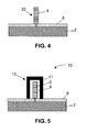
- the hardmask 4 may be removed (see Fig. 4 ). This may be done by any suitable technique known by a person skilled in the art, such as stripping.
- a dielectric layer 9 may be deposited with on top a conductive layer 11 to form a stack. Then, the stack may be patterned to form the gate 12 of the FinFET (see Fig. 5 ).
- Source and drain extensions and source and drain regions may be formed as known by a person skilled in the art.
- Figure 6 shows a top view of the device 10 as formed by the method as described above.
- the fin 5 is located between source and drain regions 13. This fin 5 is partly overlapped by the gate 12.
- the exposed area's of the underlying substrate 1, or in other words, the area's not covered by the fin 5, are modified to form the locally modified regions 6 with increased etching resistance with respect to the original buried oxide 2.
- these locally modified regions 6 with increased etching resistance protect the buried oxide 2 against influence of materials and chemicals further used during manufacturing of the FinFET 10. This prevents recesses and under-etch regions under the fin 5 to be formed in the buried oxide 2. Hence, residues of materials or chemicals further used during the manufacturing of the FinFET 10 cannot stick in these recesses and under-etch regions as they do not exist. Hence, no additional process steps are required for removing these residues.
- the substrate 1 may be a bulk semiconductor substrate.
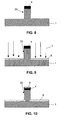
- the method according the second embodiment may be similar to the method as described for the first embodiment of the invention and is illustrated in Fig. 7 to 10 .
- the bulk semiconductor substrate 1 may be any suitable semiconductor substrate 1 onto which a semiconductor device 10 may be formed.
- the bulk semiconductor substrate 1 may be any of a bulk silicon substrate, a bulk Ge substrate, a bulk GaAs substrate, a bulk GaN substrate.
- a major surface of the bulk semiconductor substrate 1 is patterned so as to form at least one structure 20 extending from the substrate 1 having a major surface lying in a plane.
- patterning is performed in a direction substantially perpendicular to the plane of the major surface of the substrate 1.
- only one structure 20 is present on the substrate 1.
- the substrate 1 may comprise any number of structures 20 required to form a particular semiconductor device 10. Patterning of the bulk semiconductor substrate 1 may be hardmask-based or may be done by photolithography using a photoresist.
- a hardmask layer may be provided on the bulk semiconductor substrate 1.
- the hardmask layer may have a thickness of between 50 nm and 100 nm and may, for example, be 70 nm.
- the hardmask layer may, for example, comprise a metal such as e.g. Ti, Au, Ag, Pd, a nitride such as e.g. TiN, TaN, HfN, Si 3 Ni 4 , an oxide, such as e.g. TiO 2 , SiO 2 , a low-k dielectric or a combination, e.g. a stack, of the above materials.
- the thickness of the hardmask layer may preferably be such that, when implantation of implantation elements is performed in a later step of this method, the hardmask layer may act as a shield for preventing implantation elements to reach the at least one structure 20 formed (see further).
- the hardmask layer may then be patterned and etched to form hardmask 4 which only covers the bulk semiconductor substrate 1 at the location where a the at least one structure 20 is to be formed and leaves the other parts of the bulk semiconductor substrate 1 exposed (see Fig. 7 ).
- the exposed parts of the bulk semiconductor substrate 1 may then be removed, e.g. by etching. Etching may, for example, be performed by a wet etch, a dry etch or a combination thereof.
- the structure obtained after etching the bulk semiconductor substrate 1 is illustrated in Fig. 8 .
- the patterned silicon layer forms the at least one structure 20 of the semiconductor device 10.
- the at least one structure 20 can during further processing of the semiconductor device 10 be used to form e.g. a gate.
- the amount, i.e. thickness of removal of the exposed part of the bulk semiconductor substrate 1 depends on the kind of semiconductor device 10 to be formed.
- implantation of implantation elements is performed (indicated with arrows 7 in Fig. 9 ) to form locally modified regions 6 in those parts of the bulk semiconductor substrate 1 which are not covered by the at least one structure 20.
- the implantation elements are such that the etching resistance of the regions 6 which are implanted is increased. With increased etching resistance is meant that the locally modified regions 6 have a reduced etching speed with respect to the starting or original substrate 1.
- the implantation elements may be C, N, O or a combination thereof.
- an implantation dose of between 1E13 cm -2 and 1E17 cm -2 may be used.
- the hardmask 4 may act as a shield for preventing implantation elements to be implanted in the at least one structure 20. This is because the presence of implantation elements in the at least one structure 20 can lead to increased sidewall roughness of the at least one structure 20. Furthermore, the presence of implantation elements in the at least one structure 20 may lead to scattering of mobile carriers which may affect mobility of the mobile carriers in the at least one structure 20 which may later serve as e.g. a gate. According to embodiments of the invention, implantation may be performed in an anisotropic way.
- Implantation may be done in, when the bulk semiconductor substrate 1 has a major surface lying in a plane, a direction substantially perpendicular to the plane of the major surface of the substrate 1.
- substantially perpendicular is meant that the direction of implantation of the implantation elements may most preferably make an angle of between 0 and 5 degrees with the direction substantially perpendicular to the plane of the major surface of the substrate 1 such that substantially no implantation elements can enter the at least one structure 20 through its sidewalls which are not covered by the mask 4.
- substantially no implantation elements entering the at least one structure 20 is meant that a concentration of preferably less than 1 E 12 cm -2 and more preferably less than 1E10 cm -2 of implantation elements may enter the at least one structure 20 during implantation of implantation elements to form the locally modified regions 6. Therefore, most preferably, implantation may be performed with PLAD (plasma doping), as was already described in the first embodiment.
- PLAD plasma doping
- implantation of implantation elements may also be performed by any other known conventional implantation technique such as e.g. ion implantation.
- any plasma having an anisotropic character may be applied for implanting implantation elements, as long as the direction of implantation is substantially parallel to the formed structure 20 as was described above, e.g. remote plasma or RIE.
- the hardmask 4 which is still present on the at least one structure 20 may act as a shield for preventing implantation elements to be implanted into the at least one structure 20. Therefore, the thickness and the material properties of the hardmask 4 should be chosen such that after implantation only a part 8 of the hardmask 4 is implanted with implantation elements and that the implantation elements are not able to reach the at least one structure 20 (see Fig. 10 ).
- the implantation elements By implanting the implantation elements in a direction substantially parallel to the formed structure 20, preferably substantially perpendicular to the plane of the major surface of the bulk semiconductor substrate 1, no implantation elements are implanted in sidewalls of the at least one structure 20.
- the locally modified regions 6 may optionally be extended underneath the at least one structure 20. This may preferably be performed by annealing the substrate 1. Annealing may be performed at temperatures of between 800°C and 1000°C for a period of between 1 second and 60 seconds.
- the locally modified regions 6 may have a thickness t in the bulk semiconductor substrate 1 of, for example, between 1 nm and 20 nm, preferably between 1 nm and 10 nm.
- the presence of locally modified regions 6 in accordance with embodiments of the present invention may be detected by, for example, chemical analysis of the substrate, for example, by filtered transmission electron microscopy (TEM).
- TEM transmission electron microscopy
- the hardmask 4 may be removed. This may be done by any suitable technique known by a person skilled in the art, such as stripping.
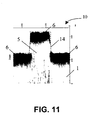
- Figure 11 shows a Scanning Spreading Resistance Measurement (SSRM) profile of a bulk FinFET, i.e. a FinFET formed on a bulk semiconductor substrate 1, in the example given a silicon substrate 1.
- a fin 6 is protruding from a bulk silicon substrate 2.
- This fin 5 is then doped using PLAD.
- implantation occurs in the regions indicated with reference number 6 and on top of the fin 5 but not in the upstanding surfaces or sidewalls 14 of the fin 5 which remain substantially unaffected by the PLAD doping process.
- these locally modified regions 6 with increased etching resistance protect the substrate 1 against influence of materials and chemicals further used during manufacturing of the semiconductor device 10. This prevents recesses and under-etch regions under the fin 5 to be formed in the substrate 1. Hence, residues of materials or chemicals further used during the manufacturing of the semiconductor device 10 cannot stick in these recesses and under-etch regions as they do not exist. Hence, no additional process steps are required for removing these residues.
- the methods according to embodiments of the invention lead to semiconductor devices with good electrical properties and good mechanical stability.
Landscapes
- Engineering & Computer Science (AREA)
- Physics & Mathematics (AREA)
- Microelectronics & Electronic Packaging (AREA)
- Condensed Matter Physics & Semiconductors (AREA)
- General Physics & Mathematics (AREA)
- Manufacturing & Machinery (AREA)
- Computer Hardware Design (AREA)
- High Energy & Nuclear Physics (AREA)
- Power Engineering (AREA)
- Toxicology (AREA)
- Health & Medical Sciences (AREA)
- Chemical & Material Sciences (AREA)
- Inorganic Chemistry (AREA)
- Thin Film Transistor (AREA)
- Insulated Gate Type Field-Effect Transistor (AREA)
Priority Applications (3)
| Application Number | Priority Date | Filing Date | Title |
|---|---|---|---|
| EP07012358A EP2009679A1 (en) | 2007-06-25 | 2007-06-25 | Semiconductor device |
| JP2008163159A JP2009038351A (ja) | 2007-06-25 | 2008-06-23 | 半導体デバイス |
| US12/145,437 US20090020786A1 (en) | 2007-06-25 | 2008-06-24 | Semiconductor device |
Applications Claiming Priority (1)
| Application Number | Priority Date | Filing Date | Title |
|---|---|---|---|
| EP07012358A EP2009679A1 (en) | 2007-06-25 | 2007-06-25 | Semiconductor device |
Publications (1)
| Publication Number | Publication Date |
|---|---|
| EP2009679A1 true EP2009679A1 (en) | 2008-12-31 |
Family
ID=38647645
Family Applications (1)
| Application Number | Title | Priority Date | Filing Date |
|---|---|---|---|
| EP07012358A Withdrawn EP2009679A1 (en) | 2007-06-25 | 2007-06-25 | Semiconductor device |
Country Status (3)
| Country | Link |
|---|---|
| US (1) | US20090020786A1 (enExample) |
| EP (1) | EP2009679A1 (enExample) |
| JP (1) | JP2009038351A (enExample) |
Families Citing this family (10)
| Publication number | Priority date | Publication date | Assignee | Title |
|---|---|---|---|---|
| US20100308440A1 (en) * | 2009-06-08 | 2010-12-09 | Globalfoundries Inc. | Semiconductor structures and methods for stabilizing silicon-comprising structures on a silicon oxide layer of a semiconductor substrate |
| JP4794692B2 (ja) * | 2009-06-24 | 2011-10-19 | パナソニック株式会社 | 半導体装置の製造方法 |
| US8193080B2 (en) * | 2009-07-27 | 2012-06-05 | Panasonic Corporation | Method for fabricating semiconductor device and plasma doping system |
| US8999798B2 (en) | 2009-12-17 | 2015-04-07 | Applied Materials, Inc. | Methods for forming NMOS EPI layers |
| US8071467B2 (en) | 2010-04-07 | 2011-12-06 | Micron Technology, Inc. | Methods of forming patterns, and methods of forming integrated circuits |
| US8357579B2 (en) * | 2010-11-30 | 2013-01-22 | Taiwan Semiconductor Manufacturing Company, Ltd. | Methods of forming integrated circuits |
| US9000498B2 (en) * | 2013-06-28 | 2015-04-07 | Stmicroelectronics, Inc. | FinFET with multiple concentration percentages |
| US9553174B2 (en) * | 2014-03-28 | 2017-01-24 | Applied Materials, Inc. | Conversion process utilized for manufacturing advanced 3D features for semiconductor device applications |
| US9589811B2 (en) * | 2015-06-24 | 2017-03-07 | Varian Semiconductor Equipment Associates, Inc. | FinFET spacer etch with no fin recess and no gate-spacer pull-down |
| US10297448B2 (en) * | 2015-11-30 | 2019-05-21 | International Business Machines Corporation | SiGe fins formed on a substrate |
Citations (3)
| Publication number | Priority date | Publication date | Assignee | Title |
|---|---|---|---|---|
| US20020037627A1 (en) * | 2000-08-10 | 2002-03-28 | Liu Mark Y. | Extension of shallow trench isolation by ion implantation |
| JP2004103899A (ja) * | 2002-09-11 | 2004-04-02 | Matsushita Electric Ind Co Ltd | 半導体装置の製造方法 |
| US20050110087A1 (en) * | 2003-11-26 | 2005-05-26 | International Business Machines Corporation ("Ibm") | Structure and method to fabricate finfet devices |
Family Cites Families (4)
| Publication number | Priority date | Publication date | Assignee | Title |
|---|---|---|---|---|
| JP3859821B2 (ja) * | 1997-07-04 | 2006-12-20 | 株式会社半導体エネルギー研究所 | 半導体装置 |
| KR100476940B1 (ko) * | 2003-06-20 | 2005-03-16 | 삼성전자주식회사 | 기판으로부터 수직으로 연장된 게이트 채널을 갖는디램기억 셀 및 그 제조방법 |
| US7384838B2 (en) * | 2005-09-13 | 2008-06-10 | International Business Machines Corporation | Semiconductor FinFET structures with encapsulated gate electrodes and methods for forming such semiconductor FinFET structures |
| DE102006030264B4 (de) * | 2006-06-30 | 2008-08-28 | Advanced Micro Devices, Inc., Sunnyvale | Verfahren zur Herstellung von Transistoren mit einem Kanal mit biaxialer Verformung, die durch Silizium/Germanium in der Gateelektrode hervorgerufen wird |
-
2007
- 2007-06-25 EP EP07012358A patent/EP2009679A1/en not_active Withdrawn
-
2008
- 2008-06-23 JP JP2008163159A patent/JP2009038351A/ja active Pending
- 2008-06-24 US US12/145,437 patent/US20090020786A1/en not_active Abandoned
Patent Citations (3)
| Publication number | Priority date | Publication date | Assignee | Title |
|---|---|---|---|---|
| US20020037627A1 (en) * | 2000-08-10 | 2002-03-28 | Liu Mark Y. | Extension of shallow trench isolation by ion implantation |
| JP2004103899A (ja) * | 2002-09-11 | 2004-04-02 | Matsushita Electric Ind Co Ltd | 半導体装置の製造方法 |
| US20050110087A1 (en) * | 2003-11-26 | 2005-05-26 | International Business Machines Corporation ("Ibm") | Structure and method to fabricate finfet devices |
Non-Patent Citations (1)
| Title |
|---|
| "INCREASED ETCH RESISTANCE OF SIO2 BY ION IMPLANTATION", IBM TECHNICAL DISCLOSURE BULLETIN, IBM CORP. NEW YORK, US, vol. 28, no. 7, December 1985 (1985-12-01), pages 3016 - 3017, XP000807048, ISSN: 0018-8689 * |
Also Published As
| Publication number | Publication date |
|---|---|
| US20090020786A1 (en) | 2009-01-22 |
| JP2009038351A (ja) | 2009-02-19 |
Similar Documents
| Publication | Publication Date | Title |
|---|---|---|
| EP2009679A1 (en) | Semiconductor device | |
| US7476578B1 (en) | Process for finFET spacer formation | |
| US5292670A (en) | Sidewall doping technique for SOI transistors | |
| CN101159233B (zh) | 用于高电压场效应晶体管的栅蚀刻工艺 | |
| JP4110085B2 (ja) | 二重ゲート型電界効果トランジスタの製造方法 | |
| US9059206B2 (en) | Epitaxial grown extremely shallow extension region | |
| EP3312876A1 (en) | Finfet device and fabrication method thereof | |
| CN1368756A (zh) | 近环绕闸极及制造具有该闸极的矽半导体装置的方法 | |
| WO2005029545A2 (en) | Self-aligned planar double-gate process by self-aligned oxidation | |
| WO2003012844A1 (en) | Xe preamorphizing implantation | |
| US11742245B2 (en) | Semiconductor fabrication method and structure using multiple sacrificial layers to form sidewall spacers | |
| CN103390586A (zh) | 形成具有提升式源极和漏极区的半导体设备的方法及对应的半导体设备 | |
| EP3217426A1 (en) | Semiconductor structure and fabrication method thereof | |
| WO2019119861A1 (zh) | 一种FinFET器件的制作方法 | |
| US20080286930A1 (en) | Nitride-encapsulated fet (nncfet) | |
| US11011556B2 (en) | Method of making a semiconductor device | |
| EP1162665A3 (en) | Trench gate MIS device and method of fabricating the same | |
| US20150001606A1 (en) | Methods and structures for a split gate memory cell structure | |
| US8610233B2 (en) | Hybrid MOSFET structure having drain side schottky junction | |
| US20070272954A1 (en) | FIN-FET device structure formed employing bulk semiconductor substrate | |
| CN107579108B (zh) | 半导体结构的形成方法 | |
| EP0225426B1 (en) | A method of fabricating a mos transistor on a substrate | |
| US6949471B2 (en) | Method for fabricating poly patterns | |
| CN104282747B (zh) | 抑制谐波效应半导体结构及形成抑制谐波效应结构的方法 | |
| CN115020239A (zh) | 半导体装置与其制造方法 |
Legal Events
| Date | Code | Title | Description |
|---|---|---|---|
| PUAI | Public reference made under article 153(3) epc to a published international application that has entered the european phase |
Free format text: ORIGINAL CODE: 0009012 |
|
| 17P | Request for examination filed |
Effective date: 20080612 |
|
| AK | Designated contracting states |
Kind code of ref document: A1 Designated state(s): AT BE BG CH CY CZ DE DK EE ES FI FR GB GR HU IE IS IT LI LT LU LV MC MT NL PL PT RO SE SI SK TR |
|
| AX | Request for extension of the european patent |
Extension state: AL BA HR MK RS |
|
| RAP1 | Party data changed (applicant data changed or rights of an application transferred) |
Owner name: IMEC |
|
| AKX | Designation fees paid |
Designated state(s): AT BE BG CH CY CZ DE DK EE ES FI FR GB GR HU IE IS IT LI LT LU LV MC MT NL PL PT RO SE SI SK TR |
|
| RAP1 | Party data changed (applicant data changed or rights of an application transferred) |
Owner name: ST MICROELECTRONICS CROLLES 2 SAS Owner name: IMEC |
|
| STAA | Information on the status of an ep patent application or granted ep patent |
Free format text: STATUS: THE APPLICATION IS DEEMED TO BE WITHDRAWN |
|
| 18D | Application deemed to be withdrawn |
Effective date: 20150106 |