EP2008263B1 - Verfahren zum ansteuern einer matrixanzeigeanordnung mit einer elektronenquelle - Google Patents
Verfahren zum ansteuern einer matrixanzeigeanordnung mit einer elektronenquelle Download PDFInfo
- Publication number
- EP2008263B1 EP2008263B1 EP07728019A EP07728019A EP2008263B1 EP 2008263 B1 EP2008263 B1 EP 2008263B1 EP 07728019 A EP07728019 A EP 07728019A EP 07728019 A EP07728019 A EP 07728019A EP 2008263 B1 EP2008263 B1 EP 2008263B1
- Authority
- EP
- European Patent Office
- Prior art keywords
- voltage
- line
- electrode
- line selection
- reference voltage
- Prior art date
- Legal status (The legal status is an assumption and is not a legal conclusion. Google has not performed a legal analysis and makes no representation as to the accuracy of the status listed.)
- Not-in-force
Links
- 238000000034 method Methods 0.000 title claims abstract description 40
- 239000011159 matrix material Substances 0.000 title claims abstract description 11
- 238000012545 processing Methods 0.000 claims description 45
- 125000004122 cyclic group Chemical group 0.000 claims description 11
- 239000003990 capacitor Substances 0.000 claims description 10
- 230000005055 memory storage Effects 0.000 claims 2
- 230000000712 assembly Effects 0.000 claims 1
- 238000000429 assembly Methods 0.000 claims 1
- 238000012800 visualization Methods 0.000 description 9
- 238000005070 sampling Methods 0.000 description 8
- 239000000463 material Substances 0.000 description 6
- OAICVXFJPJFONN-UHFFFAOYSA-N Phosphorus Chemical compound [P] OAICVXFJPJFONN-UHFFFAOYSA-N 0.000 description 4
- 230000005669 field effect Effects 0.000 description 4
- OKTJSMMVPCPJKN-UHFFFAOYSA-N Carbon Chemical compound [C] OKTJSMMVPCPJKN-UHFFFAOYSA-N 0.000 description 2
- 230000000903 blocking effect Effects 0.000 description 2
- 229910021393 carbon nanotube Inorganic materials 0.000 description 2
- 239000002041 carbon nanotube Substances 0.000 description 2
- 238000007796 conventional method Methods 0.000 description 2
- 238000010586 diagram Methods 0.000 description 2
- 230000000694 effects Effects 0.000 description 2
- 230000010287 polarization Effects 0.000 description 2
- 241000238876 Acari Species 0.000 description 1
- 230000005540 biological transmission Effects 0.000 description 1
- 239000003086 colorant Substances 0.000 description 1
- 239000002772 conduction electron Substances 0.000 description 1
- 238000005336 cracking Methods 0.000 description 1
- 230000007423 decrease Effects 0.000 description 1
- 230000001419 dependent effect Effects 0.000 description 1
- 239000003989 dielectric material Substances 0.000 description 1
- 238000000265 homogenisation Methods 0.000 description 1
- 238000012986 modification Methods 0.000 description 1
- 230000004048 modification Effects 0.000 description 1
- 229910021392 nanocarbon Inorganic materials 0.000 description 1
- 238000011160 research Methods 0.000 description 1
- 230000004044 response Effects 0.000 description 1
- 238000000926 separation method Methods 0.000 description 1
- 239000000758 substrate Substances 0.000 description 1
- 238000010200 validation analysis Methods 0.000 description 1
Images


Classifications
-
- G—PHYSICS
- G09—EDUCATION; CRYPTOGRAPHY; DISPLAY; ADVERTISING; SEALS
- G09G—ARRANGEMENTS OR CIRCUITS FOR CONTROL OF INDICATING DEVICES USING STATIC MEANS TO PRESENT VARIABLE INFORMATION
- G09G3/00—Control arrangements or circuits, of interest only in connection with visual indicators other than cathode-ray tubes
- G09G3/20—Control arrangements or circuits, of interest only in connection with visual indicators other than cathode-ray tubes for presentation of an assembly of a number of characters, e.g. a page, by composing the assembly by combination of individual elements arranged in a matrix no fixed position being assigned to or needed to be assigned to the individual characters or partial characters
- G09G3/2007—Display of intermediate tones
- G09G3/2011—Display of intermediate tones by amplitude modulation
-
- G—PHYSICS
- G09—EDUCATION; CRYPTOGRAPHY; DISPLAY; ADVERTISING; SEALS
- G09G—ARRANGEMENTS OR CIRCUITS FOR CONTROL OF INDICATING DEVICES USING STATIC MEANS TO PRESENT VARIABLE INFORMATION
- G09G3/00—Control arrangements or circuits, of interest only in connection with visual indicators other than cathode-ray tubes
- G09G3/20—Control arrangements or circuits, of interest only in connection with visual indicators other than cathode-ray tubes for presentation of an assembly of a number of characters, e.g. a page, by composing the assembly by combination of individual elements arranged in a matrix no fixed position being assigned to or needed to be assigned to the individual characters or partial characters
- G09G3/22—Control arrangements or circuits, of interest only in connection with visual indicators other than cathode-ray tubes for presentation of an assembly of a number of characters, e.g. a page, by composing the assembly by combination of individual elements arranged in a matrix no fixed position being assigned to or needed to be assigned to the individual characters or partial characters using controlled light sources
-
- G—PHYSICS
- G09—EDUCATION; CRYPTOGRAPHY; DISPLAY; ADVERTISING; SEALS
- G09G—ARRANGEMENTS OR CIRCUITS FOR CONTROL OF INDICATING DEVICES USING STATIC MEANS TO PRESENT VARIABLE INFORMATION
- G09G2310/00—Command of the display device
- G09G2310/02—Addressing, scanning or driving the display screen or processing steps related thereto
- G09G2310/0264—Details of driving circuits
- G09G2310/027—Details of drivers for data electrodes, the drivers handling digital grey scale data, e.g. use of D/A converters
-
- G—PHYSICS
- G09—EDUCATION; CRYPTOGRAPHY; DISPLAY; ADVERTISING; SEALS
- G09G—ARRANGEMENTS OR CIRCUITS FOR CONTROL OF INDICATING DEVICES USING STATIC MEANS TO PRESENT VARIABLE INFORMATION
- G09G2330/00—Aspects of power supply; Aspects of display protection and defect management
- G09G2330/02—Details of power systems and of start or stop of display operation
- G09G2330/021—Power management, e.g. power saving
-
- G—PHYSICS
- G09—EDUCATION; CRYPTOGRAPHY; DISPLAY; ADVERTISING; SEALS
- G09G—ARRANGEMENTS OR CIRCUITS FOR CONTROL OF INDICATING DEVICES USING STATIC MEANS TO PRESENT VARIABLE INFORMATION
- G09G3/00—Control arrangements or circuits, of interest only in connection with visual indicators other than cathode-ray tubes
- G09G3/20—Control arrangements or circuits, of interest only in connection with visual indicators other than cathode-ray tubes for presentation of an assembly of a number of characters, e.g. a page, by composing the assembly by combination of individual elements arranged in a matrix no fixed position being assigned to or needed to be assigned to the individual characters or partial characters
- G09G3/2007—Display of intermediate tones
- G09G3/2014—Display of intermediate tones by modulation of the duration of a single pulse during which the logic level remains constant
Definitions
- the present invention relates to a method of controlling a matrix display device having one or more electron sources capable of displaying images having different levels of gray.
- the images to display can be in black and white or in colors, in the latter case, the expression "gray level" means half-tone of color.
- the figure 1 schematically illustrates the operating principle of an exemplary electron source display device with field to which the method of the invention can be applied.
- the display device comprises electron sources 100 comprising anode electrodes 1 covered with phosphor material 2, cathode electrodes 3 electrically connected to electron-emitting zones 4, gate electrodes 5, electrically isolated from the electrodes 2.
- Each emitter zone 4 is associated with a gate electrode 5.
- the vacuum 6 reigns between the emitting zones 4 and the phosphor material 2.
- the device for controlling the electron sources 100 comprises a voltage source 7 and polarization means 8.
- the voltage source 7 makes it possible to apply a high voltage Va to the anode electrodes 1.
- the polarization means 8 allow to apply, for a given electron source 100, a potential Vg on the gate electrode associated therewith and a potential Vc1, Vc2, Vc3 on the cathode electrode 3 to which it is connected.
- the potential difference Vgc1, Vgc2, Vgc3, hereinafter generally referred to as Vgc represents the control voltage of the electron emission.
- An electron source 100 emits a stream of electrons (not shown) from its emitter zone 4 and this electron flow is collected by an anode electrode 1 which is opposite the emitting zone when the difference in potential Vgc exceeds a threshold value Vthl. This electron flow is accelerated thanks to the high voltage Va applied to the anode electrodes 1.
- the phosphor material 2 emits light under the effect of the kinetic energy of the electrons that bombard it.
- This resistance can be materialized by a layer of resistive material which covers the cathode electrodes.
- the figure 3 illustrates such a configuration.
- the gate electrodes 5 are electrically insulated from the cathode electrodes 3 by a layer of dielectric material 9.
- figure 3 the cathode electrode 3 rests on an electrically insulating substrate 110.
- the display device may have a screen 17 arranged in a matrix manner as shown in FIG. figure 4 with one or more electron sources 4.
- Each electron source 4 represents a pixel Pi, j of the screen.
- Each pixel Pi, j can be addressed and its luminance adjusted as described in the document referenced [5].
- Each pixel Pi, j is defined as the intersection between a line electrode L1, ... Li, .... Ln and a column electrode C1, ... Cj, Cm of the display device 17.
- the line electrodes L1,... Li, .... Ln are generally connected to the gate electrodes and the column electrodes C1,... Cj,... Cm to the cathode electrodes.
- the display device 17 can be reduced to a single electron source or a single pixel if only a single row electrode and a single column electrode are available or can be in a bar if has only one line electrode or one column electrode.
- a control device for controlling the display device with a line scanning generator 10 connected to a voltage source 11 delivering a voltage Vls and a reference voltage Vlns, generally ground, enabling it to apply to the line electrodes is either the line selection voltage Vls or the reference voltage Vlns or line selection voltage.
- the control device further comprises a column control circuit 12 connected to a voltage source 13 delivering a voltage Vcj and a reference voltage Vcom which can be the mass.
- the line scan generator 10 and the column control circuit 12 are connected to a screen controller 14 which receives signals from a data source (not shown), control and timing signals, and outputs signals capable of driving the line scan generator 10 and the control circuit of the columns 12.
- the anode electrodes 1 they are connected to a voltage source 15 delivering a voltage Va.
- the line scan generator includes an addressing circuit for each line electrode.
- the column control circuit includes a subcircuit for each column electrode.
- the control of the screen is carried out as follows: the line electrodes L1, Ln are addressed sequentially each in turn during a line selection period T1. An addressed line electrode is brought to the voltage Vls and an electrode unaddressed line is brought to the voltage Vlns.
- the pixels of an addressed line electrode Li must each display information given and each column electrode Cj is brought to a suitable voltage Vcj.
- the voltages applied to the column electrodes do not affect the pixels of the unaddressed line electrodes L1, Li-1, li + 1, Ln.
- To obtain gray levels one can act on the value of the differences Vls-Vcj and / or on the duration of application of the voltage Vcj or even on the quantity of charges supplied to the column electrodes and corresponding to the information to be displayed.
- Pulse width modulation (PWM) control consists in applying a fixed voltage Vc to the column electrodes for a variable time depending on the gray level to be displayed, this variable time. being less than or equal to the line selection period T1.
- the pulse width modulation control maximizes the switching between the voltage Vc and the voltage Vcom, which induces a high capacitive consumption.
- the amplitude modulation control is performed by applying a voltage Vc (k), the value of which depends on the gray level to be displayed, over the entire row selection period T1, to the column electrodes, this value being between Vc (k) max and Vcom. Consumption is minimized but it leads to inhomogeneities of low level display. Indeed, the homogenization by resistive layer as illustrated in the figure 3 is satisfactory for a high potential of the column electrode electrode electrode (or cathode gate) corresponding to the emission of white or close to white. The effect of this layer is almost zero at low level for the emission of black or near black. It has been shown both from the experimental point of view from the theoretical point of view that the uniformity of the display of carbon nanotube field emission devices, as described in the document referenced [6], deteriorates when the difference of potential electrode of column electrode of line decreases .
- the charge control method seeks to provide the column electrodes a quantity of charges corresponding to the gray level to be displayed. This control method requires in addition to a fairly complex circuitry screens having no or virtually no leakage currents.
- the patent application US 2002/0060525 discloses a method of controlling a grayscale matrix display device in which gray levels are divided into two families of gray levels, the first corresponding to the darkest gray levels and the second corresponding to the gray levels. gray less dark. If the gray level to be displayed belongs to the first family, a control voltage, applied to the columns, which is modulated in pulse width. If the gray level to be displayed belongs to the second family, a control voltage applied to the columns is used which is modulated in amplitude. These two control voltages vary in the same direction between a reference voltage and a maximum voltage. On the other hand, these two control voltages vary in opposite direction with respect to the direction of variation existing between the non-line selection voltage and the line selection voltage.
- the object of the present invention is precisely to propose a method of controlling a display device which does not have the drawbacks mentioned above.
- an object of the present invention is to propose a control method which limits the capacitive consumption and which leads to good homogeneity of the image displayed both at high level and at low level, especially in the case where a resistive layer is present between the cathode electrodes and the emitting zones.
- the present invention provides a method of controlling a matrix display device displaying gray levels comprising at least one electron source located at the intersection of a row electrode and a column electrode, applying, when the line electrode on which the electron source is located, a line selection voltage, and when a non-line selection voltage is not selected, and to apply on the corresponding column electrode a control voltage corresponding to the gray level to be displayed, during a line selection period Tl.
- the control voltage to be applied is a pulse width modulated voltage varying between a reference voltage and an extreme voltage, the direction of variation between the reference voltage and the reference voltage. extreme voltage being the same as between the no line selection voltage and the line selection voltage. The extreme voltage is positive with respect to the reference voltage.
- the control voltage to be applied is an amplitude-modulated voltage varying between the reference voltage and a maximum voltage, the direction of variation between the reference voltage and the maximum voltage being opposite to that existing between the line selection and the line selection voltage, the extreme voltage and the maximum voltage being reduced compared to those which would be necessary if the control was done for all the gray levels by modulation of amplitude or by pulse width modulation.
- the maximum voltage is negative with respect to the reference voltage.
- the line selection voltage is preferably constant throughout the line selection period.
- the method preferably consists in simultaneously applying a control voltage to each of the column electrodes relative to its electron sources.
- the method includes preferably applying a non-line selection voltage throughout the line selection period to an unselected line electrode.
- the extreme voltage and the maximum voltage are substantially equal in absolute value.
- the reference voltage can correspond to the mass.
- the present invention relates to a display device controlled by the control method thus defined, wherein the electron source comprises a resistance between an electron-emitting zone and a cathode electrode electrically connected to the line electrode.
- the present invention also relates to a control device of a matrix display device displaying gray levels comprising at least one electron source located at the intersection of a row electrode and a column electrode of a set having one or more line electrodes and one or more column electrodes.
- the device includes a line scanning generator for applying, during a line selection period, when the line electrode on which the electron source is selected, a line selection voltage, and when is not selected a line selection voltage, and a column control circuit capable of applying, on the corresponding column electrode, a control voltage corresponding to the gray level to be displayed, during the line selection period.
- the column control circuit comprises, for each column electrode of the assembly, a first processing line for delivering a voltage of a pulse width modulated control to be applied to the column electrode, if the gray level belongs to a first grayscale family containing one or more of the darkest gray levels, the control voltage modulated in width of d pulse varying between a reference voltage and an extreme voltage, the direction of variation between the reference voltage and the extreme voltage being the same as between the non-selection voltage and the line selection voltage.
- the device includes a second processing chain for providing an amplitude modulated control voltage to be applied to the column electrode, if the gray level belongs to a second gray level family containing one or more of the least gray levels.
- the amplitude-modulated control voltage varying between the reference voltage and a maximum voltage, the direction of variation between the reference voltage and the maximum voltage being opposite to that existing between the non-selection voltage of the line and the voltage of line selection.
- the extreme voltage and the maximum voltage are reduced compared to what would be necessary if the control was done for all gray levels by amplitude modulation or by pulse width modulation.
- the first processing chain may comprise means for delivering, from information coding the gray level to be displayed, a signal that reflects a start or end time of the pulse of the modulated voltage.
- width pulse in the line selection period if the gray level belongs to the first gray level family, these means being connected via logic level matching means to an output stage adapted to deliver the modulated voltage in pulse width.
- the means for delivering the signal representing the start or end time of the pulse of the pulse width modulated voltage may comprise a comparator comparing the information coding the gray level and the result of a count made by a cyclic counter counting a number of clock strokes determined by the size of the information coding the gray level, during the line selection period, and a flip-flop connected to the output of the comparator and also receiving a top in the beginning of each line selection period and outputting the signal reflecting the start or end time of the pulse of the pulse width modulated voltage.
- the control device of the display device may comprise a negative ramp generator for supplying the amplitude-modulated voltage and the second processing line may comprise means for delivering, from an information coding the level of gray that they receive, a signal which translates a negative-ramp generator's blocking-sampling instant in a line selection period, if the gray level belongs to the second gray level family, these means controlling memory means analog having an input connected to the negative ramp generator and an output connected to the input of a buffer amplifier capable of delivering the amplitude-modulated voltage.
- the means for delivering the signal representing the blocking-sampling time of the negative ramp generator may comprise a comparator comparing the information coding the gray level and the result of a count made by a cyclic counter counting a number of taps. clock determined by the size of the information coding the gray level, during the line selection period and a flip-flop connected to the output of the comparator and also receiving a peak at the beginning of each line selection period and delivering the signal translating the blocking-sampling time of the negative ramp generator.
- the cyclic counter is common to the first and the second processing chain.
- the analog storage means may comprise a switch connected on one side to the negative ramp generator and on the other to a terminal of a capacitor itself connected to the input of the buffer amplifier, the other terminal of the capacitor being brought to the reference voltage, this switch being controlled by the signal reflecting the blocking-sampling time of the negative ramp generator.
- the reference voltage at which the other terminal of the capacitor is carried is in practice generally the mass.
- the column control circuit may further comprise, by column electrode, means for selecting the first processing line or the second processing chain depending on the gray level to be displayed on the column electrode.
- the gray level to be displayed is coded in the form of a binary word with one or more bits of high weight, the selection means preferably being combinational circuits receiving the most significant bits of the binary word.
- the column control circuit may further include a shift register which supplies as many sets of storage latches as column electrodes, each set of storage latches receiving as inputs the gray levels to be displayed by the latch. viewing device and being connected to a first processing line and a second processing line.
- Each set of storage latches may also be outputted to the input of the selection means.
- This display device may be similar to that described in figure 4 which one can refer to. It comprises at least one electron source 4 materializing a pixel Pi, j.
- This electron source 4 comprises an electron-emitting zone situated at the intersection of a Li-line electrode and a column electrode Cj. It will be assumed later that the electron source is located at the crossroads of a line and a column electrode.
- the control method according to the invention consists in selecting, each in turn, the line electrodes L1, Li, Ln and to be applied to each selected line electrode during a line selection period T1 a line selection voltage Vls.
- an unselected line electrode receiving a non-line selection voltage Vlns for example the ground.
- FIG 5A shows the signal applied on a given line electrode Li during two successive line selection periods T1, the line electrode Li being selected only during the first period T1.
- the second line selection period T1 assume that it is the Li + 1 line electrode that will be selected.
- the line selection voltage Vls is applied to the line electrode Li during the first line selection period T1 and the non-line selection voltage Vlns is applied to it during the second period T1.
- line is classic.
- the Figure 6A illustrates the conventional signal to be applied to a selected line electrode in the case of pulse width modulation or amplitude modulation. Note that the amplitude of the voltage Vls' is greater than that of the voltage Vls.
- n (n integer greater than or equal to three) gray levels, these gray levels being coded between 0 and n-1.
- Code 0 corresponds to black and the code n-1 to white.
- the first F1 family has p gray levels (p integer strictly less than n), these p gray levels being coded between 0 and p-1.
- the level p-1 corresponds to the lightest gray level of the first F1 family of the darkest grays.
- the second gray level family F2 has np gray levels encoded between the p level and the n-1 level.
- the level p corresponds to the darkest gray level of the second family F2 of the lightest gray.
- a pulse width modulation will be used to display the gray levels of the first F1 family and an amplitude modulation to display the gray levels of the second family F2.
- the pulse width modulated control voltage varies between a reference voltage Vcom and an extreme voltage Vc.
- the direction of variation existing between Vcom and Vc is the same as that existing between Vlns and Vls.
- the amplitude of the pulse width modulated voltage is less than that which would be necessary if, for all the gray levels to be displayed, the control was done by modulation of pulse width.
- the amplitude modulated control voltage varies between the reference voltage and a voltage maximum Vc (k3).
- the direction of variation existing between Vcom and Vc (k3) is the inverse of that existing between Vlns and Vls.
- the amplitude of the amplitude-modulated voltage is less than that which would be necessary if, for all the gray levels to be displayed, the control was done by amplitude modulation.
- the necessary voltage corresponds to that required to switch from black to white.
- the difference between the amplitude of the pulse width modulated voltage and the maximum amplitude amplitude amplitude amplitude is substantially equal to that which would be required to display all the gray levels, if the control was only by pulse width modulation or only by amplitude modulation.
- FIG. 5B shows the shape of the voltage signal to be applied for the control of a column electrode Cj.
- a pixel Pi, j located at the intersection of this column electrode Cj and of the line electrode Li receiving the signal of the Figure 5A , a gray level of the first family F1 and secondly, on a pixel Pi + 1 j located at the intersection of this column electrode Cj and the line electrode Li + 1 which immediately follows the electrode of Li line concerned by the Figure 5A , a gray level of the second family F2.
- the gray of the first F1 family that is to say the darkest grays, in pulse width modulation mode and the excursion of the voltage to pass, in the first grayscale F1 family, from one extreme gray level to the other extreme gray level is reduced compared to what would be required to display, by pulse width modulation, all the gray levels .
- the Figure 6B which shows the voltage signal to be applied to the column electrode in the case of a conventional pulse width modulation, the amplitude of this voltage being substantially twice that of the Figure 5B .
- p is therefore provided with different values for the first time range T, each of these p values corresponding to one of the p gray levels of the first F1 family of grayscale.
- this voltage Vc (k) is negative with respect to the reference voltage Vcom or is equal to the reference voltage Vcom.
- the amplitude of this voltage Vc (k) depends on the gray level to be displayed belonging to the second family F2 of gray levels.
- np voltages Vc (k) corresponding to the np gray levels of this second family F2 of gray levels are provided.
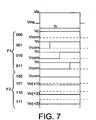
- the voltage Vc (k3) is the one which has the greatest amplitude in absolute value on the figure 7 .
- This capacitive consumption is divided by four in the case of the method of the invention compared to the conventional method of pulse width modulation since the voltage has been divided by two.
- Another advantage of the method of the invention compared with the conventional pulse width modulation method is that the use of the two families of gray levels makes it possible to reduce the number of time slots to be managed during the selection period. line, which is to say that the cutoff frequency is increased accordingly.
- the maximum amplitude of the voltage to be switched is now -20 volts whereas it would have been -40 volts with a conventional modulation method amplitude.
- FIG. 7 shows for a display with 8 gray levels, the voltage signals to be applied on a column electrode to obtain each of these levels.
- the first chronogram shows, for the record, the voltage signal applied to a line electrode of the screen of the display device. It is assumed that the eight gray levels have been divided into two families F1, F2 of four levels each.
- the first family F1 encompasses the darkest black and grays respectively coded in binary 000, 001, 010, 011.
- the second family F2 includes the least dark gray and white respectively coded in binary 100, 101, 110, 111.
- Vc (k1), Vc (k2), Vc (k3) are negative with respect to the reference potential Vcom.
- the voltage applied to the columns in the case of gray levels of the second family F2 (for which the command is an amplitude modulation) is added to the line selection voltage at a selected pixel.
- the emission threshold of a field effect source is more defined by a contrast ratio or emission current than by a well-marked value.
- the threshold chosen is the line selection voltage.
- the control voltage of the columns takes the same value, a current contribution equal to that selected for the threshold for the pixels of each unselected line displaying this voltage, from which a leak can be multiplied by more than 1000 for a complete high definition screen, that is to say the order of magnitude of the expected contrast.
- the darkest grayscale of a given pixel depends on the voltages presented on its column for the display of the other pixels of its column during a frame time. As a result, either drastically limits the adjustable control voltage to be applied to the columns and hence the current excursion between the black and the white and therefore the contrast of the screen, ie the darkest gray levels are degraded and vary according to the image.
- lighter gray levels can be displayed by providing a column control voltage which is reduced for non-selected lines, while limiting the switching amplitude for displaying the most gray levels. dark and therefore capacitive consumption.
- the present invention also relates to a control device of an electron source matrix display device capable of displaying gray levels.
- FIGs 8A and 8B the control device of an electron source matrix display device for displaying gray levels according to the invention is shown schematically.
- the display device 25 comprises at least one electron source Pi, j located at the crossroads of a line electrode on the one hand and a column electrode on the other hand, this line electrode and this electrode of column that is part of a set of one or more rows and one or more columns.
- the electron source Pi, j materializes a pixel.
- the controller of the display device typically comprises a scan generator of one or more lines 22 and a control circuit of one or more columns 23.
- the control circuit of the columns 23 is connected to a digital data source 20 capable of providing binary words coding on s bits the gray level to be displayed by a pixel.
- the control device of the display device also comprises a screen controller 21 and a ramp generator 24 with a negative slope.
- the screen controller 21 receives synchronization signals from the data source 20, it manages and provides signals adapted to drive the line scan generator 22 and the control circuit of the columns 23.
- the negative ramp generator 24 is connected to the control circuit of the columns 23, the latter can perform for a given column, a sample blocking a voltage VR of this negative ramp and then apply it to the associated column electrode.
- the voltages VR delivered are negative with respect to the reference voltage Vcom or equal thereto.
- FIG. 8C shows schematically the shape of the voltage VR delivered by the negative ramp generator 24 and the different voltage levels that can be obtained to display the gray levels of the second family F2 of gray levels during a sampling blocking.
- This figure is based on the example of figure 7 for which one had to have three gray levels corresponding to the voltages Vc (k1), Vc (k2), Vc (k3).
- the scan generator of the lines 22 is conventional and will not be described in more detail because it does not pose a problem to a person skilled in the art.
- the column control circuit includes a shift register 40 serving as an address decoder.
- This shift register 40 has m outputs and propagates m times the selection bit CSI by the clock signal SCK.
- the m outputs of the shift register 40 drive as many sets 41 of flip-flops (latches in English) than column electrodes c1 to cm, each of them cooperating with one of the column electrodes c1 to cm of the display device 25 illustrated in FIG. figure 8A .
- the sets 41 comprise s storage latches. These latches 41 of storage latches also receive data words encoding the information to be displayed delivered by the digital data source 20 which they store with the clock signal SCK when the shift register 40 validates said set 41 of flip-flops. storage.
- each of the m sets 41 of memory latches supplies firstly a first processing chain 30 intended to deliver the voltage control signal to be applied to the associated column electrode when the gray level to be displayed belongs to the first F1 grayscale family and secondly a second processing chain 31 for delivering the voltage control signal to be applied to the associated column electrode when the gray level to be displayed belongs to the second family F2 gray levels.
- the outputs of these first and second processing chains 30, 31 are connected to a column electrode c1 to cm which is the associated column electrode.
- the output of each of the m sets 41 of storage latches is also connected to input means 47 for selecting either the first processing line 30 or the second processing chain 31 according to the gray level to be displayed on the electrode. associated column.
- the selection means 47 may be combinational logic circuits which use q (q ⁇ 1) most significant bits of the words encoding the information to be displayed present at the output of the set 41 of associated storage latches.
- This first processing chain 30 comprises, in cascade, means 32 for delivering, from information relating to the gray level to be displayed, that they receive a message. signal which, if the control is to be done by modulation of pulse width, translates the beginning or the end of the pulse of the modulated voltage into pulse width.
- This output stage 53 is formed of three switches Q1, Q2, Q3 of which only one can be closed at a time.
- switches Q1, Q2, Q3, two switches Q1, Q2 cooperate with the first processing chain 30 and the third Q3 with the second processing chain 31.
- These switches Q1, Q2, Q3 may be transistors as shown in FIGS. Figures 8B and 9 .
- This output stage 53 is capable of delivering the pulse width modulated signal to be applied to the associated column electrode.
- the two transistors Q1 and Q2 which cooperate with the first processing line 30 are mounted in push-pull between the extreme voltage Vc and the reference voltage Vcom.
- the transistor Q1 makes it possible to switch the voltage Vc on the associated column electrode while the transistor Q2 makes it possible to impose the reference voltage Vcom.
- the means 32 for delivering the signal representing the beginning or the end of the pulse of the pulse width modulated voltage may comprise a comparator 43 receiving, on its first inputs, the output of the storage latches of the set. 41 to which it is connected and s seconds inputs the result of a count performed by a cyclic counter 42, clocked by a CCP clock and reset by an LC load signal warning of the beginning of each new line selection period.
- the counter 42 counts from 0 to 2 s -1 during the line selection period T1. It can be envisaged that the means 32 for delivering the signal representing the beginning or the end of the pulse of the pulse-modulated voltage do not receive. all the bits of the words coding the gray levels, but only those that are significant as we will see later.
- the comparator 43 compares the information relating to the gray level and the result of the counting performed by the cyclic counter 42 counting a number of CCP clock strokes determined by the size of the information relative to the gray level, during the period of time. line selection.
- the comparator 43 therefore changes state at a given instant which corresponds to the moment when the counting result of the cyclic counter 42 coincides with the data. present on the first inputs of the comparator 43.
- the means 32 for outputting the signal representing the beginning or the end of the pulse of the modulated pulse width signal also comprise at the output of the comparator 43 a flip-flop 44 (flip-flop). flop). This flip-flop 44 also receives as input the loading signal LC. This flip-flop 44 toggles as soon as the signals arriving on its two inputs have loaded.
- the flip-flop 44 connected to the output of the comparator 43 also receives a peak at the beginning of each line selection period and delivers the signal representing the start or end time of the pulse of the pulse width modulated voltage.
- the output of the flip-flop 44 is connected to the transistors Q1, Q2 of the output stage 53 at their control gate, via the logic level adapter means 45.
- the output stage 53 is able to switch according to of the signal that it receives from the flip-flop 44, either the reference voltage Vcom (transistor Q2 passing and transistor Q1 off), or the extreme voltage Vc positive with respect to the reference voltage (transistor Q1 and transistor Q2 blocked) either of these two voltages according to the validation delivered by the selection means 47.
- the third transistor Q3 of the output stage is on and the two transistors Q1 and Q2 are off.
- the logic level adapter means 45 translate the amplitude of the signal that translates the start or end time of the pulse width modulated voltage pulse which is a logic signal to obtain a signal whose amplitude is appropriate to the respective control of the transistors Q1 and Q2. They are connected as input to the output of the selection means 47.
- the selection means 47 made by a combinational circuit allow to allow or not the switching of the transistors Q1, Q2 of the first processing chain 30 if the q most significant bits of the data delivered by the set 41 of memory latches associated are the darkest gray levels.
- q 1 and the output stage 53 could switch between Vcom and Vc, thanks to the signals applied to the gates of the transistors Q1, Q2 coming from the output of the flip-flop 44 if the high-order bit q is worth 0.
- This second processing chain 31 comprises, in cascade, means 33 for delivering, from the information relating to the gray level they receive, a signal which , if of course the command must be done by amplitude modulation, translates a moment of blocking-sampling ramp generator 24 with a negative slope.
- These means 33 feed analog storage means 51.
- the analog storage means 51 have their output connected to the input of a buffer amplifier 52 whose output is connected to the associated column electrode via the switch Q3 of the output stage 53.
- this switch Q3 made in the example by a transistor.
- the transistor Q3 is mounted between the associated column electrode and the output of the buffer amplifier 52.
- the buffer amplifier 52 is able to deliver to the associated column electrode, when it is enabled by the transistor Q3 which is then passing, the voltage modulated in amplitude.
- the means 33 for delivering the signal expressing the blocking-sampling instant may comprise, as for the first processing chain 30, a comparator 49 receiving on its first inputs the output of the storage latches of the set 41 to which it is connected. connected and s s seconds inputs the result of a count performed by a cyclic counter 48, clocked by a clock CCN and reset by the LC load signal. It can be envisaged that the means 33 for delivering the signal representing the blocking-sampling instant do not receive all the bits of the words coding the gray levels, but only those that are significant as will be seen later.
- the comparator 49 compares the information relating to the gray level and the result of a count made by the cyclic counter 48 counting a number CCN clock ticks determined by the size of the gray level information during the line selection period.
- the comparator 49 therefore changes state at a given instant which corresponds to the moment when the counting result of the counter 48 coincides with the data present on the first inputs of the comparator 49.
- the means 33 for delivering the signal reflecting the sampling-blocking time also comprise, connected at the output of the comparator 49, a bistable flip-flop 50 (flip-flop). This flip-flop 50 receives as input the loading signal LC and the output of the comparator 49. This flip-flop 50 switches as soon as the signals arriving on its two inputs have changed.
- the flip-flop 50 is connected at the output to the input of the analog storage means 51 whose output is connected to the input of the buffer amplifier 52.
- the analog storage means 51 comprise a storage capacitor C1 whose terminal is connected to the output of the ramp generator (represented by the denomination VR) via a switch I1. This terminal is also connected to the input of the buffer amplifier 52. The other terminal of the capacitor C1 is brought to a reference voltage, generally ground. This reference voltage may be different from Vcom.
- the switch I1 is controlled by the output of the flip-flop 50. The opening of the switch I1 makes it possible to memorize in the capacitor C1 the voltage level delivered by the ramp generator 24 just before opening.
- the buffer amplifier 52 can to be performed by an amplifier capable of copying, the voltage delivered by the analog storage means 51. If the transistor Q3 is conducting, it delivers the current to the control of the associated column electrode.
- the on or off state of the transistor Q3 is controlled by logic level matching means 46 connected between the gate of the transistor Q3 and the output of the selection means 47.
- the logic level matching means 46 connected to the gate of the transistor Q3, translates the logic signal from the selection means 47 into a signal whose amplitude is appropriate to the control of the transistor Q3.
- the selection means 47 enable the voltage from the buffer amplifier 52 to be switched on the associated column electrode in the manner of what has been described above for the first processing line 30, but now the q Most significant bits of the words coding the information delivered by the associated latch 41 must correspond to the darkest gray levels. In the example of the figure 7 the buffer amplifier 52 of the second processing chain 31 would be validated if the high-order bit q is 1.
- the buffer amplifier 52 delivers, when it is turned on by the transistor Q3, the amplitude-modulated voltage at the associated column.
- a comparator 43 comparator assembly 42 makes it possible to adjust the switching time of the reference voltage Vcom or the inverse of the switching time of the voltage. extreme positive Vc.
- a meter assembly 48, comparator 49 makes it possible to choose the moment of the opening of the switch I1 and thus to memorize the level of the voltage Vc (k) negative with respect to the reference voltage Vcom.
- the Figure 8B is only an exemplary embodiment of the control of the column electrodes of the display device.
Landscapes
- Engineering & Computer Science (AREA)
- Physics & Mathematics (AREA)
- Computer Hardware Design (AREA)
- General Physics & Mathematics (AREA)
- Theoretical Computer Science (AREA)
- Control Of Indicators Other Than Cathode Ray Tubes (AREA)
Claims (22)
- Verfahren zum Ansteuern einer Graupegel anzeigenden Matrixanzeigeanordnung mit wenigstens einer an der Kreuzung einer Zeilenelektrode (Li) und einer Spaltenelektrode (Cj) befindlichen Elektronenquelle (Pi,j), darin bestehend, während einer Zeilenselektionsperiode (Tl), wenn die Elektrode (Li) der Zeile, in der sich die Elektronenquelle (Pi,j) befindet, selektiert wird, eine Zeilenselektionsspannung (Vls) anzulegen, und, wenn sie nicht selektiert wird, eine Nicht-Zeilenselektionsspannung (Vlns), und an die entsprechende Spaltenelektrode (Cj) eine dem anzuzeigenden Graupegel entsprechende Ansteuerungsspannung anzulegen,
dadurch gekennzeichnet, dass man die anzuzeigenden Graupegel in zwei Graupegelgruppen (F1, F2) unterteilt, wobei die erste (F1) den oder die dunkelsten Graupegel umfasst und die zweite (F2) den oder die hellsten Graupegel,
und dadurch, dass, wenn der anzuzeigende Graupegel zu der ersten Gruppe (F1) gehört, die anzulegende Ansteuerungsspannung eine zwischen einer Referenzspannung (Vcom) und einer Extremspannung (Vc) variierende impulsbreitenmodulierte Spannung ist, wobei die Richtung der Variation zwischen der Referenzspannung und der Extremspannung dieselbe ist wie zwischen der Nicht-Zeilenselektionspannung und der Zeilenselektionsspannung,
und dadurch, dass, wenn der anzuzeigende Graupegel zu der zweiten Gruppe (F2) gehört, die anzulegende Ansteuerungsspannung eine zwischen der Referenzspannung (Vcom) und einer Maximalspannung (Vc(k3)) variierende amplitudenmodulierte Spannung ist, wobei die Richtung der Variation zwischen der Referenzspannung und der Maximalspannung derjenigen entgegengesetzt ist, die zwischen der Nicht-Zeilenselektionsspannung (Vlns) und der Zeilenselektionsspannung (Vls) existiert,
wobei die Extremspannung und die Maximalspannung klein sind in Bezug auf diejenigen, die notwendig wären, wenn die Ansteuerung für alle Graupegel durch Amplitudenmodulation oder durch Impulsbreitenmodulation erfolgen würde. - Verfahren nach Anspruch 1, dadurch gekennzeichnet, dass die Extremspannung (Vc) positiv ist in Bezug auf die Referenzspannung (Vcom), und dadurch, dass die Maximalspannung (Vc(k3)) negativ ist in Bezug auf die Referenzspannung (Vcom).
- Verfahren nach einem der Ansprüche 1 oder 2, bei dem:wenn der anzuzeigende Graupegel zu der ersten Gruppe (F1) gehört, die Ansteuerungsspannung während einer ersten Zeitspanne (T, 0<T≤T1) die Extremspannung (Vc) ist, die konstant ist, und in dem Maße, wie die erste Zeitspanne (T) strikt kleiner ist als die Zeilenselektionsperiode (T1), die Ansteuerungsspannung während einer der ersten Zeitspanne (t) vorausgehenden oder folgenden zweiten Zeitspanne (T'=T1-T) die Referenzspannung (Vcom) ist, wobei der Wert der ersten Zeitspanne T von dem anzuzeigenden Graupegel abhängt, und,wenn der anzuzeigende Graupegel zu der zweiten Gruppe (F2) gehört, die Ansteuerungsspannung während der gesamten Zeilenselektionsperiode (Tl) eine konstante Spannung ist, negativ in Bezug auf die Referenzspannung (Vcom) oder gleich der Referenzspannung, wobei diese Ansteuerungsspannung eine Amplitude hat, die von dem anzuzeigenden Graupegel abhängt.
- Verfahren nach einem der Ansprüche 1 bis 3, dadurch gekennzeichnet, dass die Zeilenansteuerungsspannung (Vls) während der gesamten Zeilenselektionsperiode (Tl) konstant ist.
- Verfahren nach einem der Ansprüche 1 bis 4, dadurch gekennzeichnet, dass es, wenn mehrere Elektronenquellen auf einer selben Zeilenelektrode (Li) sind, darin besteht, simultan an jede der diese Elektronenquellen betreffenden Spaltenelektroden (C1, Cj, Cm) eine Ansteuerungsspannung (Vc) anzulegen.
- Verfahren nach einem der Ansprüche 1 bis 5, dadurch gekennzeichnet, dass es darin besteht, die Nicht-Zeilenselektionsspannung (Vlns) während der gesamten Zeilenselektionsperiode (Tl) an eine nicht selektierte Zeilenelektrode (Li+1) anzulegen.
- Verfahren nach einem der Ansprüche 1 bis 6, dadurch gekennzeichnet, dass die Extremspannung (Vc) und die Maximalspannung (Vc(k3)) als Absolutwert im Wesentlichen gleich sind.
- Verfahren nach einem der Ansprüche 1 bis 7, dadurch gekennzeichnet, dass die Referenzspannung (Vcom) der Masse entspricht.
- Vorrichtung zum Ansteuern einer Graupegel anzeigenden Matrixanzeigeanordnung mit wenigstens einer an der Kreuzung einer Zeilenelektrode (Li) und einer Spaltenelektrode (Cj) befindlichen Elektronenquelle eines Systems mit einer oder mehreren Zeilenelektroden und einer oder mehreren Spaltenelektroden, einen Abtastgenerator (22) der Zeilen umfassend, um während einer Zeilenselektionsperiode (Tl), wenn die Zeilenelektrode (Li), auf der sich die Elektronenquelle befindet, selektiert wird, eine Zeilenselektionsspannung (Vls) anzulegen, und, wenn sie nicht selektiert wird, eine Nicht-Zeilenselektionsspannung (Vlns),
und eine Spaltenansteuerungsschaltung (23), fähig während der Zeilenselektionsperiode an eine entsprechende Spaltenelektrode (Cj) eine Ansteuerungsspannung entsprechend dem anzuzeigenden Graupegel anzulegen,
dadurch gekennzeichnet, dass die Spaltenansteuerungsschaltung (23) für jede Spaltenelektrode des Systems umfasst:eine erste Verarbeitungskette (30), um eine impulsbreitenmodulierte Ansteuerungsspannung zu liefern, anzulegen an die Spaltenelektrode, wenn der Graupegel zu einer ersten Gruppe (F1) von Graupegeln mit einem oder mehreren der dunkelsten Graupegel gehört, wobei die impulsbreitenmodulierte Ansteuerungsspannung zwischen einer Referenzspannung (Vcom) und einer Extremspannung (Vc) variiert und die Richtung der Variation zwischen der Referenzspannung (Vcom) und der Extremspannung (Vc) dieselbe ist wie zwischen der Nicht-Zeilenselektionspannung (Vlns) und der Zeilenselektionsspannung (Vls), und,eine zweite Verarbeitungskette (31), um eine amplitudenmodulierte Ansteuerungsspannung zu liefern, anzulegen an die Spaltenelektrode (Cj), wenn der Graupegel zu einer zweiten Gruppe (F2) von Graupegeln mit einem oder mehreren der hellsten Graupegel gehört, wobei die amplitudenmodulierte Ansteuerungsspannung zwischen einer Referenzspannung (Vcom) und einer Maximalspannung (Vc(k3)) variiert und die Richtung der Variation zwischen der Referenzspannung (Vcom) und der Maximalspannung (Vc(k3)) derjenigen entgegengesetzt ist, die zwischen der Nicht-Zeilenselektionspannung (Vlns) und der Zeilenselektionsspannung (Vls) existiert,wobei die Extremspannung (Vc) und die Maximalspannung (Vc(k3)) klein sind in Bezug auf diejenigen, die notwendig wären, wenn die Ansteuerung für alle Graupegel durch Amplitudenmodulation oder durch Impulsbreitenmodulation erfolgen würde. - Vorrichtung nach Anspruch 9, dadurch gekennzeichnet, dass die Extremspannung (Vc) positiv ist in Bezug auf die Referenzspannung (Vcom), und dadurch, dass die Maximalspannung (Vc(k3)) negativ ist in Bezug auf die Referenzspannung (Vcom).
- Vorrichtung nach einem der Ansprüche 9 oder 10, dadurch gekennzeichnet, dass die erste Verarbeitungskette (30) Einrichtungen (32) umfasst, um aufgrund einer Information, die sie erhalten, die anzuzeigenden Graupegel zu codieren, um ein Signal zu liefern, das einen Anfangs- oder Endzeitpunkt des Impulses der impulsbreitenmodulierten Spannung in der Zeilenselektionsperiode (Tl) wiedergibt, wenn der Graupegel zu der ersten Graupegelgruppe (F1) gehört, wobei diese Einrichtungen (32) über Adaptionseinrichtungen logischer Pegel (45) mit einer Ausgangsstufe (53) verbunden sind, welche die impulsbreitenmodulierte Spannung liefert.
- Vorrichtung nach Anspruch 11, dadurch gekennzeichnet, dass die Einrichtungen (32) zur Lieferung des den Anfangs- oder Endzeitpunkt des Impulses der impulsbreitenmodulierten Spannung wiedergebenden Signals einen Komparator (43) umfassen, der vergleicht: die Information, die den Graupegel und das Resultat einer durch einen zyklischen Zähler (42) realisierten Zählung codiert, der eine Anzahl von Taktimpulsen (CCP), bestimmt durch die Größe der den Graupegel codierenden Information, während der Zeilenselektionsperiode (Tl) zählt, und eine bistabile Kippstufe (44), die verbunden ist mit dem Ausgang des Komparators (43) und ebenfalls zu Beginn jeder Zeilenselektionsperiode (Tl) ein Top (LC) empfängt und das Signal liefert, das den Anfangs- oder Endzeitpunkt des Impulses der impulsbreitenmodulierten Spannung wiedergibt.
- Vorrichtung nach einem der Ansprüche 9 bis 12, dadurch gekennzeichnet, dass sie einen Negativrampengenerator (24) umfasst, der ermöglicht, die amplitudenmodulierte Spannung zu liefern, und dadurch, dass die zweite Verarbeitungskette (31) Einrichtungen (33) umfasst, um aufgrund einer Information, die den Graupegel codiert, den sie empfangen, ein Signal zu liefern, das in einer Zeilenselektionsperiode (Tl) einen Abtast-Halte-Zeitpunkt des Negativrampengenerators (24) in einer Zeilenselektionsperiode (Tl) wiedergibt, wenn der Graupegel zu der zweiten Graupegelgruppe (F2) gehört, wobei diese Einrichtungen (33) analoge Speichereinrichtungen (51) ansteuern, die einen mit dem Negativrampengenerator (24) verbundenen Eingang und einen Ausgang hat, der verbunden ist mit dem Eingang eines Pufferverstärkers (52), der fähig ist, die amplitudenmodulierte Spannung zu liefern.
- Vorrichtung nach Anspruch 13, dadurch gekennzeichnet, dass die Einrichtungen (33) zum Liefern des den Abtast-Halte-Zeitpunkt wiedergebenden Signals des Negativrampengenerators (24) einen Komparator (49) umfasst, der vergleicht: die Information, die den Graupegel und das Resultat einer durch einen zyklischen Zähler (48) realisierten Zählung codiert, der eine Anzahl von Taktimpulsen (CCN), bestimmt durch die Größe der den Graupegel codierenden Information, während der Zeilenselektionsperiode (Tl) zählt, und eine bistabile Kippstufe (50), die verbunden ist mit dem Ausgang des Komparators (49) und ebenfalls zu Beginn jeder Zeilenselektionsperiode (Tl) ein Top (LC) empfängt und das Signal liefert, das den Anfangs- oder Endzeitpunkt des Negativrampengenerators (24) wiedergibt.
- Vorrichtung nach einem der Ansprüche 12 oder 14, dadurch gekennzeichnet, dass der zyklische Zähler (60) ein gemeinsamer Zähler der ersten und der zweiten Verarbeitungskette ist.
- Vorrichtung nach einem der Ansprüche 13 bis 15, dadurch gekennzeichnet, dass die analogen Speichereinrichtungen (51) einen Schalter (I1) umfassen, einerseits mit dem Negativrampengenerator (24) verbunden und andererseits mit dem Anschluss eines Kondensators (C1), seinerseits selbst mit dem Eingang des Pufferverstärkers (52) verbunden, wobei der andere Anschluss des Kondensators (C1) an eine Referenzspannung bzw. ein Referenzpotential gelegt ist und der Schalter (I1) durch das Signal gesteuert wird, das den Abtast-Halte-Zeitpunkt des Negativrampengenerators (24) wiedergibt.
- Vorrichtung nach Anspruch 16, dadurch gekennzeichnet, dass die Referenzspannung bzw. das Referenzpotential, an das der andere Anschluss des Kondensators (C1) gelegt ist, die Masse ist.
- Vorrichtung nach einem der Ansprüche 9 bis 17, dadurch gekennzeichnet, dass die Spaltenansteuerungsschaltung außerdem, als Spaltenelektrode (C1), Selektionseinrichtungen (47) der ersten Verarbeitungskette (30) oder der zweiten Verarbeitungskette (31) umfasst, in Abhängigkeit von dem auf der Spaltenelektrode (C1) anzuzeigenden Graupegel.
- Vorrichtung nach Anspruch 18, dadurch gekennzeichnet, dass der anzuzeigende Graupegel in Form eines binären Wortes mit einem oder mehreren höherwertigen Bits (q) codiert wird, wobei die Selektionseinrichtungen (47) kombinatorische Schaltungen sind, die die höherwertigen Bits (q) des binären Worts empfangen.
- Vorrichtung nach einem der Ansprüche 9 bis 19, dadurch gekennzeichnet, dass die Spaltenansteuerungsschaltung außerdem ein Schieberegister (40) umfasst, das ebenso viele Speicherkippstufeneinheiten (41) wie Spaltenelektroden (C1, Cm) versorgt, wobei jede Speicherkippstufeneinheit (41) am Eingang die durch die Anzeigevorrichtung anzuzeigenden Graupegel erhält und mit einer ersten Verarbeitungskette (30) und einer zweiten Verarbeitungskette (31) verbunden ist.
- Vorrichtung nach Anspruch 20 in seiner Verbindung mit Anspruch 18, dadurch gekennzeichnet, dass jede Speicherkippstufeneinheit (41) mit dem Ausgang auch mit dem Eingang der Selektionseinrichtungen (47) verbunden ist.
- Anzeigevorrichtung, die Vorrichtung des Anspruchs 9 umfassend, bei der die Elektronenquelle (4) einen Widerstand (R1) zwischen einer Elektronenemissionszone (4) und einer elektrisch mit der Zeilenelektrode verbundenen Kathodenelektrode (3) umfasst.
Applications Claiming Priority (2)
| Application Number | Priority Date | Filing Date | Title |
|---|---|---|---|
| FR0603413A FR2899991B1 (fr) | 2006-04-14 | 2006-04-14 | Procede de commande d'un dispositif de visualisation matriciel a source d'electrons |
| PCT/EP2007/053551 WO2007122112A1 (fr) | 2006-04-14 | 2007-04-12 | Procédé de commande d'un dispositif de visualisation matriciel a source d'électrons |
Publications (2)
| Publication Number | Publication Date |
|---|---|
| EP2008263A1 EP2008263A1 (de) | 2008-12-31 |
| EP2008263B1 true EP2008263B1 (de) | 2012-05-16 |
Family
ID=37036783
Family Applications (1)
| Application Number | Title | Priority Date | Filing Date |
|---|---|---|---|
| EP07728019A Not-in-force EP2008263B1 (de) | 2006-04-14 | 2007-04-12 | Verfahren zum ansteuern einer matrixanzeigeanordnung mit einer elektronenquelle |
Country Status (4)
| Country | Link |
|---|---|
| US (1) | US20100156943A1 (de) |
| EP (1) | EP2008263B1 (de) |
| FR (1) | FR2899991B1 (de) |
| WO (1) | WO2007122112A1 (de) |
Families Citing this family (2)
| Publication number | Priority date | Publication date | Assignee | Title |
|---|---|---|---|---|
| US9668840B2 (en) | 2010-12-20 | 2017-06-06 | Koninklijke Philips N.V. | Oral hygiene appliance with bristle characteristics for effective cleaning |
| JP2024024216A (ja) * | 2022-08-09 | 2024-02-22 | 株式会社Jvcケンウッド | 液晶表示装置 |
Family Cites Families (9)
| Publication number | Priority date | Publication date | Assignee | Title |
|---|---|---|---|---|
| FR2623013A1 (fr) * | 1987-11-06 | 1989-05-12 | Commissariat Energie Atomique | Source d'electrons a cathodes emissives a micropointes et dispositif de visualisation par cathodoluminescence excitee par emission de champ,utilisant cette source |
| FR2708129B1 (fr) * | 1993-07-22 | 1995-09-01 | Commissariat Energie Atomique | Procédé et dispositif de commande d'un écran fluorescent à micropointes. |
| KR100192429B1 (ko) * | 1996-10-24 | 1999-06-15 | 구본준 | 액정표시소자의 구동장치 |
| JP2002156938A (ja) * | 2000-11-21 | 2002-05-31 | Canon Inc | 画像表示装置およびその駆動方法 |
| US7079161B2 (en) * | 2001-06-14 | 2006-07-18 | Canon Kabushiki Kaisha | Image display apparatus |
| FR2832537B1 (fr) * | 2001-11-16 | 2003-12-19 | Commissariat Energie Atomique | Procede et dispositif de commande en tension d'une source d'electrons a structure matricielle, avec regulation de la charge emise |
| JP3715967B2 (ja) * | 2002-06-26 | 2005-11-16 | キヤノン株式会社 | 駆動装置及び駆動回路及び画像表示装置 |
| FR2880173B1 (fr) * | 2004-12-28 | 2007-05-11 | Commissariat Energie Atomique | Procede de commande d'un ecran de visualisation matriciel |
| FR2907959B1 (fr) * | 2006-10-30 | 2009-02-13 | Commissariat Energie Atomique | Procede de commande d'un dispositif de visualisation matriciel a source d'electrons a consommation capacitive reduite |
-
2006
- 2006-04-14 FR FR0603413A patent/FR2899991B1/fr not_active Expired - Fee Related
-
2007
- 2007-04-12 WO PCT/EP2007/053551 patent/WO2007122112A1/fr not_active Ceased
- 2007-04-12 EP EP07728019A patent/EP2008263B1/de not_active Not-in-force
- 2007-04-12 US US12/296,235 patent/US20100156943A1/en not_active Abandoned
Also Published As
| Publication number | Publication date |
|---|---|
| EP2008263A1 (de) | 2008-12-31 |
| FR2899991B1 (fr) | 2009-03-20 |
| FR2899991A1 (fr) | 2007-10-19 |
| WO2007122112A1 (fr) | 2007-11-01 |
| US20100156943A1 (en) | 2010-06-24 |
Similar Documents
| Publication | Publication Date | Title |
|---|---|---|
| EP0635819B1 (de) | Verfahren und Einrichtung zur Steuerung einer Mikrospitzenanzeigevorrichtung | |
| EP0597772B1 (de) | Multiplexbetriebener Matrixbildschirm und Steuerverfahren dafür | |
| FR2683365A1 (fr) | Dispositif d'affichage a panneau plat a emission de champ et circuit de compensation d'irregulatites utilisable dans un tel dispositif d'affichage. | |
| FR2569294A1 (fr) | Panneau d'affichage et son procede de commande | |
| FR2738654A1 (fr) | Procede de pilotage pour un affichage plasma permettant un affichage d'echelle de gris ameliore et affichage plasma correspondant | |
| FR2626705A1 (fr) | Montage d'affichage a matrice integree | |
| FR2772502A1 (fr) | Procede de compensation des differences de remanence des luminophores dans un ecran de visualisation d'images | |
| FR2826768A1 (fr) | Procede de pilotage de dispositif d'affichage a plasma | |
| FR2757676A1 (fr) | Dispositif d'emission de champ a faible tension d'excitation | |
| EP0485285B1 (de) | Elektrooptische bistabile Vorrichtung, eine solche Vorrichtung enthaltender Bildschirm und Steuerungsverfahren dazu | |
| EP2008263B1 (de) | Verfahren zum ansteuern einer matrixanzeigeanordnung mit einer elektronenquelle | |
| EP1851747B1 (de) | Pixeladressierungsschaltung und verfahren zur steuerung solcher schaltung | |
| EP2084698B1 (de) | Verfahren zur ansteuerung einer matrixanzeigeanordnung mit einer elektronenquelle mit verringertem kapazitiven verbrauch | |
| FR2691568A1 (fr) | Procédé d'affichage de différents niveaux de gris et système de mise en Óoeuvre de ce procédé. | |
| FR2739712A1 (fr) | Procede et appareil de modulation de niveaux de gris d'un affichage matriciel | |
| EP1299876B1 (de) | Verfahren und vorrichtung zur steuerung einer elektronenquelle in matrixstruktur, mit regulierung durch die emittierte ladung | |
| EP1313088A1 (de) | Verfahren und Vorrichtung zur Spannungssteuerung einer Elektronenquelle mit Matrixstruktur, mit Regulierung von emittierter Ladung | |
| EP0292376A1 (de) | Elektrolumineszenzanzeigeeinrichtung mit Speichereffekt und mit Halbton | |
| EP1677277B1 (de) | Verfahren zur Steuerung einer Matrix-Anzeige | |
| EP1354309A1 (de) | Digitaler video-bildschirm | |
| EP1958182B1 (de) | Videosystem mit einer durch ein verbessertes adressierungsverfahren gesteuerten flussigkristallmatrixanzeige | |
| EP1771838B1 (de) | Bildanzeigevorrichtung und steuerungsverfahren für die anzeigevorrichtung | |
| FR2580826A1 (fr) | Procede et appareil de commande d'un dispositif de modulation optique | |
| EP1958183B1 (de) | Sequentielle farbbeleuchtungs-flüssigkristall-matrixanzeige |
Legal Events
| Date | Code | Title | Description |
|---|---|---|---|
| PUAI | Public reference made under article 153(3) epc to a published international application that has entered the european phase |
Free format text: ORIGINAL CODE: 0009012 |
|
| 17P | Request for examination filed |
Effective date: 20081006 |
|
| AK | Designated contracting states |
Kind code of ref document: A1 Designated state(s): AT BE BG CH CY CZ DE DK EE ES FI FR GB GR HU IE IS IT LI LT LU LV MC MT NL PL PT RO SE SI SK TR |
|
| AX | Request for extension of the european patent |
Extension state: AL BA HR MK RS |
|
| GRAP | Despatch of communication of intention to grant a patent |
Free format text: ORIGINAL CODE: EPIDOSNIGR1 |
|
| RIN1 | Information on inventor provided before grant (corrected) |
Inventor name: SARRASIN, DENIS |
|
| GRAS | Grant fee paid |
Free format text: ORIGINAL CODE: EPIDOSNIGR3 |
|
| RAP1 | Party data changed (applicant data changed or rights of an application transferred) |
Owner name: COMMISSARIAT A L'ENERGIE ATOMIQUE ET AUX ENERGIES |
|
| GRAA | (expected) grant |
Free format text: ORIGINAL CODE: 0009210 |
|
| DAX | Request for extension of the european patent (deleted) | ||
| AK | Designated contracting states |
Kind code of ref document: B1 Designated state(s): AT BE BG CH CY CZ DE DK EE ES FI FR GB GR HU IE IS IT LI LT LU LV MC MT NL PL PT RO SE SI SK TR |
|
| REG | Reference to a national code |
Ref country code: GB Ref legal event code: FG4D Free format text: NOT ENGLISH |
|
| REG | Reference to a national code |
Ref country code: CH Ref legal event code: EP |
|
| REG | Reference to a national code |
Ref country code: AT Ref legal event code: REF Ref document number: 558405 Country of ref document: AT Kind code of ref document: T Effective date: 20120615 |
|
| REG | Reference to a national code |
Ref country code: IE Ref legal event code: FG4D Free format text: LANGUAGE OF EP DOCUMENT: FRENCH |
|
| REG | Reference to a national code |
Ref country code: DE Ref legal event code: R096 Ref document number: 602007022663 Country of ref document: DE Effective date: 20120719 |
|
| REG | Reference to a national code |
Ref country code: NL Ref legal event code: VDEP Effective date: 20120516 |
|
| REG | Reference to a national code |
Ref country code: LT Ref legal event code: MG4D Effective date: 20120516 |
|
| PG25 | Lapsed in a contracting state [announced via postgrant information from national office to epo] |
Ref country code: FI Free format text: LAPSE BECAUSE OF FAILURE TO SUBMIT A TRANSLATION OF THE DESCRIPTION OR TO PAY THE FEE WITHIN THE PRESCRIBED TIME-LIMIT Effective date: 20120516 Ref country code: IS Free format text: LAPSE BECAUSE OF FAILURE TO SUBMIT A TRANSLATION OF THE DESCRIPTION OR TO PAY THE FEE WITHIN THE PRESCRIBED TIME-LIMIT Effective date: 20120916 Ref country code: LT Free format text: LAPSE BECAUSE OF FAILURE TO SUBMIT A TRANSLATION OF THE DESCRIPTION OR TO PAY THE FEE WITHIN THE PRESCRIBED TIME-LIMIT Effective date: 20120516 Ref country code: PL Free format text: LAPSE BECAUSE OF FAILURE TO SUBMIT A TRANSLATION OF THE DESCRIPTION OR TO PAY THE FEE WITHIN THE PRESCRIBED TIME-LIMIT Effective date: 20120516 Ref country code: SE Free format text: LAPSE BECAUSE OF FAILURE TO SUBMIT A TRANSLATION OF THE DESCRIPTION OR TO PAY THE FEE WITHIN THE PRESCRIBED TIME-LIMIT Effective date: 20120516 Ref country code: CY Free format text: LAPSE BECAUSE OF FAILURE TO SUBMIT A TRANSLATION OF THE DESCRIPTION OR TO PAY THE FEE WITHIN THE PRESCRIBED TIME-LIMIT Effective date: 20120516 |
|
| REG | Reference to a national code |
Ref country code: AT Ref legal event code: MK05 Ref document number: 558405 Country of ref document: AT Kind code of ref document: T Effective date: 20120516 |
|
| PG25 | Lapsed in a contracting state [announced via postgrant information from national office to epo] |
Ref country code: LV Free format text: LAPSE BECAUSE OF FAILURE TO SUBMIT A TRANSLATION OF THE DESCRIPTION OR TO PAY THE FEE WITHIN THE PRESCRIBED TIME-LIMIT Effective date: 20120516 Ref country code: GR Free format text: LAPSE BECAUSE OF FAILURE TO SUBMIT A TRANSLATION OF THE DESCRIPTION OR TO PAY THE FEE WITHIN THE PRESCRIBED TIME-LIMIT Effective date: 20120817 Ref country code: SI Free format text: LAPSE BECAUSE OF FAILURE TO SUBMIT A TRANSLATION OF THE DESCRIPTION OR TO PAY THE FEE WITHIN THE PRESCRIBED TIME-LIMIT Effective date: 20120516 Ref country code: PT Free format text: LAPSE BECAUSE OF FAILURE TO SUBMIT A TRANSLATION OF THE DESCRIPTION OR TO PAY THE FEE WITHIN THE PRESCRIBED TIME-LIMIT Effective date: 20120917 |
|
| PG25 | Lapsed in a contracting state [announced via postgrant information from national office to epo] |
Ref country code: AT Free format text: LAPSE BECAUSE OF FAILURE TO SUBMIT A TRANSLATION OF THE DESCRIPTION OR TO PAY THE FEE WITHIN THE PRESCRIBED TIME-LIMIT Effective date: 20120516 Ref country code: NL Free format text: LAPSE BECAUSE OF FAILURE TO SUBMIT A TRANSLATION OF THE DESCRIPTION OR TO PAY THE FEE WITHIN THE PRESCRIBED TIME-LIMIT Effective date: 20120516 Ref country code: SK Free format text: LAPSE BECAUSE OF FAILURE TO SUBMIT A TRANSLATION OF THE DESCRIPTION OR TO PAY THE FEE WITHIN THE PRESCRIBED TIME-LIMIT Effective date: 20120516 Ref country code: DK Free format text: LAPSE BECAUSE OF FAILURE TO SUBMIT A TRANSLATION OF THE DESCRIPTION OR TO PAY THE FEE WITHIN THE PRESCRIBED TIME-LIMIT Effective date: 20120516 Ref country code: CZ Free format text: LAPSE BECAUSE OF FAILURE TO SUBMIT A TRANSLATION OF THE DESCRIPTION OR TO PAY THE FEE WITHIN THE PRESCRIBED TIME-LIMIT Effective date: 20120516 Ref country code: RO Free format text: LAPSE BECAUSE OF FAILURE TO SUBMIT A TRANSLATION OF THE DESCRIPTION OR TO PAY THE FEE WITHIN THE PRESCRIBED TIME-LIMIT Effective date: 20120516 Ref country code: EE Free format text: LAPSE BECAUSE OF FAILURE TO SUBMIT A TRANSLATION OF THE DESCRIPTION OR TO PAY THE FEE WITHIN THE PRESCRIBED TIME-LIMIT Effective date: 20120516 |
|
| PG25 | Lapsed in a contracting state [announced via postgrant information from national office to epo] |
Ref country code: IT Free format text: LAPSE BECAUSE OF FAILURE TO SUBMIT A TRANSLATION OF THE DESCRIPTION OR TO PAY THE FEE WITHIN THE PRESCRIBED TIME-LIMIT Effective date: 20120516 |
|
| PLBE | No opposition filed within time limit |
Free format text: ORIGINAL CODE: 0009261 |
|
| STAA | Information on the status of an ep patent application or granted ep patent |
Free format text: STATUS: NO OPPOSITION FILED WITHIN TIME LIMIT |
|
| 26N | No opposition filed |
Effective date: 20130219 |
|
| PG25 | Lapsed in a contracting state [announced via postgrant information from national office to epo] |
Ref country code: ES Free format text: LAPSE BECAUSE OF FAILURE TO SUBMIT A TRANSLATION OF THE DESCRIPTION OR TO PAY THE FEE WITHIN THE PRESCRIBED TIME-LIMIT Effective date: 20120827 |
|
| REG | Reference to a national code |
Ref country code: DE Ref legal event code: R097 Ref document number: 602007022663 Country of ref document: DE Effective date: 20130219 |
|
| PG25 | Lapsed in a contracting state [announced via postgrant information from national office to epo] |
Ref country code: BG Free format text: LAPSE BECAUSE OF FAILURE TO SUBMIT A TRANSLATION OF THE DESCRIPTION OR TO PAY THE FEE WITHIN THE PRESCRIBED TIME-LIMIT Effective date: 20120816 |
|
| BERE | Be: lapsed |
Owner name: COMMISSARIAT A L'ENERGIE ATOMIQUE ET AUX ENERGIES Effective date: 20130430 |
|
| PG25 | Lapsed in a contracting state [announced via postgrant information from national office to epo] |
Ref country code: MC Free format text: LAPSE BECAUSE OF FAILURE TO SUBMIT A TRANSLATION OF THE DESCRIPTION OR TO PAY THE FEE WITHIN THE PRESCRIBED TIME-LIMIT Effective date: 20120516 |
|
| REG | Reference to a national code |
Ref country code: CH Ref legal event code: PL |
|
| GBPC | Gb: european patent ceased through non-payment of renewal fee |
Effective date: 20130412 |
|
| REG | Reference to a national code |
Ref country code: IE Ref legal event code: MM4A |
|
| PG25 | Lapsed in a contracting state [announced via postgrant information from national office to epo] |
Ref country code: GB Free format text: LAPSE BECAUSE OF NON-PAYMENT OF DUE FEES Effective date: 20130412 Ref country code: CH Free format text: LAPSE BECAUSE OF NON-PAYMENT OF DUE FEES Effective date: 20130430 Ref country code: BE Free format text: LAPSE BECAUSE OF NON-PAYMENT OF DUE FEES Effective date: 20130430 Ref country code: DE Free format text: LAPSE BECAUSE OF NON-PAYMENT OF DUE FEES Effective date: 20131101 Ref country code: LI Free format text: LAPSE BECAUSE OF NON-PAYMENT OF DUE FEES Effective date: 20130430 |
|
| REG | Reference to a national code |
Ref country code: FR Ref legal event code: ST Effective date: 20131231 |
|
| REG | Reference to a national code |
Ref country code: DE Ref legal event code: R119 Ref document number: 602007022663 Country of ref document: DE Effective date: 20131101 |
|
| PG25 | Lapsed in a contracting state [announced via postgrant information from national office to epo] |
Ref country code: FR Free format text: LAPSE BECAUSE OF NON-PAYMENT OF DUE FEES Effective date: 20130430 |
|
| PG25 | Lapsed in a contracting state [announced via postgrant information from national office to epo] |
Ref country code: IE Free format text: LAPSE BECAUSE OF NON-PAYMENT OF DUE FEES Effective date: 20130412 |
|
| PG25 | Lapsed in a contracting state [announced via postgrant information from national office to epo] |
Ref country code: MT Free format text: LAPSE BECAUSE OF FAILURE TO SUBMIT A TRANSLATION OF THE DESCRIPTION OR TO PAY THE FEE WITHIN THE PRESCRIBED TIME-LIMIT Effective date: 20120516 |
|
| PG25 | Lapsed in a contracting state [announced via postgrant information from national office to epo] |
Ref country code: TR Free format text: LAPSE BECAUSE OF FAILURE TO SUBMIT A TRANSLATION OF THE DESCRIPTION OR TO PAY THE FEE WITHIN THE PRESCRIBED TIME-LIMIT Effective date: 20120516 |
|
| PG25 | Lapsed in a contracting state [announced via postgrant information from national office to epo] |
Ref country code: LU Free format text: LAPSE BECAUSE OF NON-PAYMENT OF DUE FEES Effective date: 20130412 Ref country code: HU Free format text: LAPSE BECAUSE OF FAILURE TO SUBMIT A TRANSLATION OF THE DESCRIPTION OR TO PAY THE FEE WITHIN THE PRESCRIBED TIME-LIMIT; INVALID AB INITIO Effective date: 20070412 |