EP2007179A9 - Multilayer circuit board having cable portion and method for manufacturing same - Google Patents
Multilayer circuit board having cable portion and method for manufacturing same Download PDFInfo
- Publication number
- EP2007179A9 EP2007179A9 EP07737869A EP07737869A EP2007179A9 EP 2007179 A9 EP2007179 A9 EP 2007179A9 EP 07737869 A EP07737869 A EP 07737869A EP 07737869 A EP07737869 A EP 07737869A EP 2007179 A9 EP2007179 A9 EP 2007179A9
- Authority
- EP
- European Patent Office
- Prior art keywords
- layer
- board
- boards
- holes
- layer board
- Prior art date
- Legal status (The legal status is an assumption and is not a legal conclusion. Google has not performed a legal analysis and makes no representation as to the accuracy of the status listed.)
- Granted
Links
Images


Classifications
-
- H—ELECTRICITY
- H05—ELECTRIC TECHNIQUES NOT OTHERWISE PROVIDED FOR
- H05K—PRINTED CIRCUITS; CASINGS OR CONSTRUCTIONAL DETAILS OF ELECTRIC APPARATUS; MANUFACTURE OF ASSEMBLAGES OF ELECTRICAL COMPONENTS
- H05K3/00—Apparatus or processes for manufacturing printed circuits
- H05K3/46—Manufacturing multilayer circuits
- H05K3/4611—Manufacturing multilayer circuits by laminating two or more circuit boards
- H05K3/4626—Manufacturing multilayer circuits by laminating two or more circuit boards characterised by the insulating layers or materials
-
- H—ELECTRICITY
- H05—ELECTRIC TECHNIQUES NOT OTHERWISE PROVIDED FOR
- H05K—PRINTED CIRCUITS; CASINGS OR CONSTRUCTIONAL DETAILS OF ELECTRIC APPARATUS; MANUFACTURE OF ASSEMBLAGES OF ELECTRICAL COMPONENTS
- H05K3/00—Apparatus or processes for manufacturing printed circuits
- H05K3/46—Manufacturing multilayer circuits
-
- H—ELECTRICITY
- H05—ELECTRIC TECHNIQUES NOT OTHERWISE PROVIDED FOR
- H05K—PRINTED CIRCUITS; CASINGS OR CONSTRUCTIONAL DETAILS OF ELECTRIC APPARATUS; MANUFACTURE OF ASSEMBLAGES OF ELECTRICAL COMPONENTS
- H05K1/00—Printed circuits
- H05K1/02—Details
- H05K1/11—Printed elements for providing electric connections to or between printed circuits
- H05K1/118—Printed elements for providing electric connections to or between printed circuits specially for flexible printed circuits, e.g. using folded portions
-
- H—ELECTRICITY
- H05—ELECTRIC TECHNIQUES NOT OTHERWISE PROVIDED FOR
- H05K—PRINTED CIRCUITS; CASINGS OR CONSTRUCTIONAL DETAILS OF ELECTRIC APPARATUS; MANUFACTURE OF ASSEMBLAGES OF ELECTRICAL COMPONENTS
- H05K3/00—Apparatus or processes for manufacturing printed circuits
- H05K3/46—Manufacturing multilayer circuits
- H05K3/4688—Composite multilayer circuits, i.e. comprising insulating layers having different properties
- H05K3/4691—Rigid-flexible multilayer circuits comprising rigid and flexible layers, e.g. having in the bending regions only flexible layers
-
- H—ELECTRICITY
- H05—ELECTRIC TECHNIQUES NOT OTHERWISE PROVIDED FOR
- H05K—PRINTED CIRCUITS; CASINGS OR CONSTRUCTIONAL DETAILS OF ELECTRIC APPARATUS; MANUFACTURE OF ASSEMBLAGES OF ELECTRICAL COMPONENTS
- H05K2201/00—Indexing scheme relating to printed circuits covered by H05K1/00
- H05K2201/01—Dielectrics
- H05K2201/0183—Dielectric layers
- H05K2201/0195—Dielectric or adhesive layers comprising a plurality of layers, e.g. in a multilayer structure
-
- H—ELECTRICITY
- H05—ELECTRIC TECHNIQUES NOT OTHERWISE PROVIDED FOR
- H05K—PRINTED CIRCUITS; CASINGS OR CONSTRUCTIONAL DETAILS OF ELECTRIC APPARATUS; MANUFACTURE OF ASSEMBLAGES OF ELECTRICAL COMPONENTS
- H05K2201/00—Indexing scheme relating to printed circuits covered by H05K1/00
- H05K2201/09—Shape and layout
- H05K2201/09209—Shape and layout details of conductors
- H05K2201/095—Conductive through-holes or vias
- H05K2201/09509—Blind vias, i.e. vias having one side closed
- H05K2201/09518—Deep blind vias, i.e. blind vias connecting the surface circuit to circuit layers deeper than the first buried circuit layer
-
- H—ELECTRICITY
- H05—ELECTRIC TECHNIQUES NOT OTHERWISE PROVIDED FOR
- H05K—PRINTED CIRCUITS; CASINGS OR CONSTRUCTIONAL DETAILS OF ELECTRIC APPARATUS; MANUFACTURE OF ASSEMBLAGES OF ELECTRICAL COMPONENTS
- H05K2203/00—Indexing scheme relating to apparatus or processes for manufacturing printed circuits covered by H05K3/00
- H05K2203/05—Patterning and lithography; Masks; Details of resist
- H05K2203/0548—Masks
- H05K2203/0554—Metal used as mask for etching vias, e.g. by laser ablation
-
- H—ELECTRICITY
- H05—ELECTRIC TECHNIQUES NOT OTHERWISE PROVIDED FOR
- H05K—PRINTED CIRCUITS; CASINGS OR CONSTRUCTIONAL DETAILS OF ELECTRIC APPARATUS; MANUFACTURE OF ASSEMBLAGES OF ELECTRICAL COMPONENTS
- H05K3/00—Apparatus or processes for manufacturing printed circuits
- H05K3/0011—Working of insulating substrates or insulating layers
- H05K3/0017—Etching of the substrate by chemical or physical means
- H05K3/002—Etching of the substrate by chemical or physical means by liquid chemical etching
-
- H—ELECTRICITY
- H05—ELECTRIC TECHNIQUES NOT OTHERWISE PROVIDED FOR
- H05K—PRINTED CIRCUITS; CASINGS OR CONSTRUCTIONAL DETAILS OF ELECTRIC APPARATUS; MANUFACTURE OF ASSEMBLAGES OF ELECTRICAL COMPONENTS
- H05K3/00—Apparatus or processes for manufacturing printed circuits
- H05K3/22—Secondary treatment of printed circuits
- H05K3/28—Applying non-metallic protective coatings
- H05K3/281—Applying non-metallic protective coatings by means of a preformed insulating foil
-
- H—ELECTRICITY
- H05—ELECTRIC TECHNIQUES NOT OTHERWISE PROVIDED FOR
- H05K—PRINTED CIRCUITS; CASINGS OR CONSTRUCTIONAL DETAILS OF ELECTRIC APPARATUS; MANUFACTURE OF ASSEMBLAGES OF ELECTRICAL COMPONENTS
- H05K3/00—Apparatus or processes for manufacturing printed circuits
- H05K3/38—Improvement of the adhesion between the insulating substrate and the metal
- H05K3/386—Improvement of the adhesion between the insulating substrate and the metal by the use of an organic polymeric bonding layer, e.g. adhesive
Definitions
- the present invention relates to a multilayer circuit board having flexible cable portions and a method for manufacturing the same, and more specifically to a structure of a buildup-type multilayer circuit board equipped with flexible cable portions having a plurality of layers and a method for manufacturing the same.
- Figure 5 is a sectional view showing the main configuration of a conventional multilayer circuit board having cable portions drawn out of a plurality of layers.
- a flexible insulating base material 101 of polyimide or the like which is a basic material
- layers to be the cable portions of a flexible circuit board 102 having circuit patterns including cable portions on both surfaces are disposed, and cover lays 105 having adhesive materials 104 on insulating films 103, such as polyimide films, are adhered onto the layers to be the cable portions to form cables for the outer-layer boards 106 and the inner-layer board 107 (refer to Patent Document 1).
- the cables for the outer-layer boards 106 and the inner-layer board 107 are bonded by previously punched adhesive materials 108.
- adhesive materials 108 For interlayer connection, through-holes penetrating all the layers, and blind via holes connecting nearby layers are used.
- Patent Document 2 Aside from this, a method for manufacturing a thin multilayer flexible circuit board has also been provided (refer to Patent Document 2). This is for manufacturing a thin four-layer flexible circuit board by sharing the cover film for a flexible circuit board to become the cable portions of the inner-layer board with the base material for the outer-layer boards, that is, the flexible insulating base material.
- Patent Document 1 has a problem in that since the configuration of the multilayer portion 109 is complicated and thick, the requirement for thickness reduction cannot be satisfied.
- the desmear processing for removing foreign matter, such as the chips becomes complicated, and the lack of desmear processing causes defective electrical connection.
- the number of composing material is increased, there is a problem of increase in material costs.
- the present invention has been made in consideration of the above-described aspects, and it is an object of the present invention to provide a multilayer flexible circuit board that can be configured to be thin even though the board has cable portions drawn out of a plurality of outer layers; and a method for manufacturing the same.
- the present invention provides a multilayer flexible circuit board, which is the first invention; and a method for manufacturing the same, which is the second invention.
- the first aspect of the present invention is a multilayer flexible circuit board including a parts mounting portion having an inner-layer board and outer-layer boards, and cable portions drawn out of at least one of the inner-layer board and outer-layer boards, wherein each of the inner-layer board and the outer-layer boards has circuits facing one another, characterized by each of the circuits facing one another is covered with a cover formed of a cover film in common with the cable portion.
- the second aspect of the present invention is a method for manufacturing a multilayer flexible circuit board including a parts mounting portion having an inner-layer board and outer-layer boards laminated one another, each having a base material and conductive layers, and cable portions drawn out of at least one of the inner-layer board and outer-layer boards, wherein each of the inner-layer board and the outer-layer boards has circuits facing one another, characterized by including:
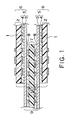
- Figure 1 is a sectional view showing the structure of a multilayer flexible circuit board being Embodiment 1 of the present invention.
- This shows circuit boards 2 where circuit patterns including cable portions are formed on flexible insulating base materials 1, which are base materials.
- the circuit boards 2 are used as outer-layer boards.
- cover lays 5 wherein an adhesive material 4 is overlaid on each of insulating films 3, such as polyimide, are adhered onto either upper or lower surfaces, shown in the drawing, of the circuit boards 2.
- an adhesive material 4 is overlaid on each of insulating films 3, such as polyimide, are adhered onto either upper or lower surfaces, shown in the drawing, of the circuit boards 2.
- a double-sided inner-layer board 9 having circuit patterns on the upper and lower surfaces, shown in the drawing, of the base material is prepared. Then, in the state wherein cover lays 5 are inserted, the outer-layer boards 6 are adhered onto both surfaces, shown in the drawing, of the inner-layer board 9.
- Previously punched adhesives 8 are adhered onto the inner-layer board 9, and the insulating films 3 of the cover lays 5 are adhered by the adhesives 8 to form the cover lays 5. Then, the outer-layer boards 6 are continuously joined to the inner-layer board 9 by the cover lays 3. Thereby, the multilayer portion wherein the outer-layer boards 6 and the inner-layer board 9 are laminated is configured to be thin.
- the portions drawn out of both the outer-layer boards 6 and the inner-layer board 9 are used as flexible cables, and the portions are drawn out of at least one of the outer-layer boards 6 and the inner-layer board 9.
- FIG 2 is process diagrams showing part of processes in the method for manufacturing Embodiment 1 shown in Figure 1 .
- a conductive hole 24 is formed using an NC drill or the like in a base material 21 composed of a flexible insulating material, such as polyimide, of a thickness of for example, 25 ⁇ m having copper foils 22 and 23 of thickness of 8 ⁇ m on the both surfaces, which is called a double-sided copper clad laminate.
- the inner-layer board 9 is formed.
- conducting treatment and subsequent electrolytic plating treatment are performed on the conductive hole 24 opened in the base material 21 to form an electrolytic-plated film 25 of about 10 ⁇ m, and an interlayer conducting path is formed. Thereby, a penetrating conductive hole 26 is formed.
- circuit patterns on the both surfaces are subjected to a series of processes, such as resist layer formation, exposure, development, etching, and resist layer peeling using a photo fabrication method to form circuit patterns 27. Thereby, a double-sided inner-layer board 9 is formed.
- the alignment accuracy can be easily secured without being affected by the elongation and shrinkage of the material.
- an exposing machine that can perform highly accurate alignment may be used.
- a roughening treatment for improving adhesion to the adhesive material may also be carried out.
- a cover lay 5 having an adhesive material 4, such as acryl and epoxy of a thickness of 15 ⁇ m on an insulating film 3, which is a polyimide film of a thickness of for example, 12 ⁇ m is prepared. Then, the cover lay 5 is adhered onto the inner-layer side of the buildup layer of the multilayer circuit board using a vacuum press, a laminator, or the like. Thereby, the outer-layer boards 6 with the cover lays 5 can be obtained.
- adhesive materials 8 for laminating the outer-layer boards 6 on the inner-layer board 7 are aligned.
- the adhesive materials 8 are previously punched.
- the outer-layer boards 6 with the cover lays 5 and the inner-layer board 7 are laminated with intervening adhesive materials 8 by the vacuum press or the like to form a multilayer circuit.
- the adhesive material a material with little runoff, such as a low-flow type prepreg and a bonding sheet, is preferred.
- the thickness of the adhesive material 8 is preferably about 15 ⁇ m.
- Figure 3 (4) shows a process for etching off the base materials 1 using the conformal masks 28a. In this process, the base materials 1 of the outer-layer boards 6 on the portions of the conductive holes 31 and the inner-layer boards 9 are removed.
- a resin etchant a solution containing an alkali metal, an amine compound and water is preferred.
- the polyimide film of the base material 1 which is the flexible insulating base material can be selectively removed, and the adhesive material 4 of acryl, epoxy, or the like is little affected. Therefore, the polyimide film of the base material 1 to be removed can be subjected to resin etching without the shortage of etching.
- a polyimide film for the base material 1 of the outer-layer boards 6 obtained by the polycondensation of pyromellitic dianhydride and aromatic diamine having high etching rate (for example, Kapton manufactured by du Pont and Apical manufactured by Kaneka Corporation) is preferred.
- a polyimide film obtained by the polycondensation of biphenyl tetracarbonic dianhidride and diaminobenzene (for example, Upilex manufactured by Ube Industries, Ltd.) is preferred.
- a resin film having high resistance to the above-described resin etchant such as aramid resin may be used instead of polyimide.
- step via holes and skip via holes are formed in the cover lays 5 and the adhesive materials 8 exposed from the conductive holes 31 processed in resin etching.
- laser processing is performed using previously prepared conformal masks 28a and 29a to form three kinds of conductive holes 31, 31a and 31b.
- the laser method may be selected from UV-YAG laser, carbon dioxide laser, excimer laser or the like.
- the diameters of respective conductive holes 31, 31a and 31b are determined as follows: Firstly, the diameter of the conductive holes 31 is determined to be 50 ⁇ m, because when polyimide of a thickness of 25 ⁇ m is used for the base material 1, conductive holes having a diameter of 50 ⁇ m can be fabricated, and the plating thickness required for securing reliability is about 10 ⁇ m.
- the hole diameter that can secure reliability when plating thickness is about 15 to 20 ⁇ m
- the upper hole diameter is 150 ⁇ m and the lower hole diameter is 150 ⁇ m in the conductive holes 31a
- minute wirings can be formed and the degree of integration can also be improved.
- desmear treatment and conduction treatment for performing the interlayer connection by electrolytic plating are carried out.
- a direct laser method may also be combined.
- the thickness of the copper foil is preferably 20 ⁇ m or less.
- unnecessary adhesive materials 32 on the inner-layer board 9 can also be removed by laser processing.
- the kind of laser used in this case is preferably excimer laser, which excels in processing accuracy in the depth direction.
- the multilayer circuit base material having conductive holes 31, 31a and 31b is subjected to electrolytic plating of about 15 to 20 ⁇ m to achieve interlayer conduction.
- electrolytic plating of about 15 to 20 ⁇ m to achieve interlayer conduction.
- skip via holes 35 obtained from conductive holes 31 can be formed, and the interlayer conduction of all the circuits from the outer-layer boards to the inner-layer board in the buildup board can be achieved.
- a multilayer circuit base material wherein interlayer conduction has been completed is obtained.
- through-holes may be formed using an NC drill or the like at the time of forming conductive holes, and the through-holes may also be simultaneously formed at the time of via hole plating.
- circuit patterns 36 for the outer-layer boards are formed using a normal photo fabrication method. At this time, plating layers deposited on the cover films 3 located in the inner-layer side of the laminated board are also removed, if any.
- a multilayer circuit board 37 having cables drawn out of the outer-layer boards 6 and the inner-layer board 7 can be formed.
- a multilayer circuit board having cable portions in the inner-layer board and the outer-layer board include the followings.
- the multilayer flexible circuit board enabling high-density mounting for digital video cameras can mount a CSP (chip size package), and requires cables that are repeatedly bent and cables from other layers to be bent when assembled in the housing.
- CSP chip size package
- the requirements can be fully satisfied by using cables in the outer-layer board 6 as cables for repeated bending, and using cables in the inner-layer board 7 in combination as cables from other layers to be bent when assembled in the housing.
- the circuit provided on one of the base materials of the outer-layer boards and the inner-layer board of which cable portions can be drawn out composes the multilayer flexible circuit board coated by the cover common to the cable portions
- the laminate structure can be simplified, and the multilayer flexible circuit board having a reduced thickness can be provided.
- material costs can be reduced, the cost reduction effect can be obtained.
- the method for manufacturing a multilayer flexible circuit board wherein manufacturing processes are simplified can be provided.
- via holes for connecting the outer-layer boards to the inner-layer board since mask holes for forming conductive holes in the circuit pattern are provided, and the conductive holes are formed using the mask holes, highly reliable conductive holes integrated with the circuit pattern can be obtained.
Abstract
Description
- The present invention relates to a multilayer circuit board having flexible cable portions and a method for manufacturing the same, and more specifically to a structure of a buildup-type multilayer circuit board equipped with flexible cable portions having a plurality of layers and a method for manufacturing the same.
-
Figure 5 is a sectional view showing the main configuration of a conventional multilayer circuit board having cable portions drawn out of a plurality of layers. On a flexibleinsulating base material 101 of polyimide or the like, which is a basic material, layers to be the cable portions of aflexible circuit board 102 having circuit patterns including cable portions on both surfaces are disposed, and cover lays 105 havingadhesive materials 104 oninsulating films 103, such as polyimide films, are adhered onto the layers to be the cable portions to form cables for the outer-layer boards 106 and the inner-layer board 107 (refer to Patent Document 1). - The cables for the outer-
layer boards 106 and the inner-layer board 107 are bonded by previously punchedadhesive materials 108. For interlayer connection, through-holes penetrating all the layers, and blind via holes connecting nearby layers are used. - Aside from this, a method for manufacturing a thin multilayer flexible circuit board has also been provided (refer to Patent Document 2). This is for manufacturing a thin four-layer flexible circuit board by sharing the cover film for a flexible circuit board to become the cable portions of the inner-layer board with the base material for the outer-layer boards, that is, the flexible insulating base material.
- Patent Document 1: Japanese Patent Publication No.
2-55958 - Patent Document 2: Japanese Patent Laid-Open No.
5-90757 - Among the above-described structures, what is described in
Patent Document 1 has a problem in that since the configuration of themultilayer portion 109 is complicated and thick, the requirement for thickness reduction cannot be satisfied. In addition, when perforating conducting holes upon the formation of through-holes and blind via holes, there is another problem of dealing with the generation of a large quantity of foreign matter, such as the chips of materials for each layer and smear, in the conducting holes. Specifically, there are possibilities that the desmear processing for removing foreign matter, such as the chips, becomes complicated, and the lack of desmear processing causes defective electrical connection. Also, since the number of composing material is increased, there is a problem of increase in material costs. - Also in the method described in
Patent Document 2, since the formation of outer-layer cables is difficult, it is still not easy to manufacture a thin multilayer flexible circuit board. - The present invention has been made in consideration of the above-described aspects, and it is an object of the present invention to provide a multilayer flexible circuit board that can be configured to be thin even though the board has cable portions drawn out of a plurality of outer layers; and a method for manufacturing the same.
- To achieve the above-described object, the present invention provides a multilayer flexible circuit board, which is the first invention; and a method for manufacturing the same, which is the second invention.
- The first aspect of the present invention is a multilayer flexible circuit board including a parts mounting portion having an inner-layer board and outer-layer boards, and cable portions drawn out of at least one of the inner-layer board and outer-layer boards, wherein each of the inner-layer board and the outer-layer boards has circuits facing one another, characterized by each of the circuits facing one another is covered with a cover formed of a cover film in common with the cable portion.
- The second aspect of the present invention is a method for manufacturing a multilayer flexible circuit board including a parts mounting portion having an inner-layer board and outer-layer boards laminated one another, each having a base material and conductive layers, and cable portions drawn out of at least one of the inner-layer board and outer-layer boards, wherein each of the inner-layer board and the outer-layer boards has circuits facing one another, characterized by including:
- a process for preparing the inner-layer board and outer-layer boards;
- a process for forming a circuit pattern having mask holes for forming conducting holes in the conductive layer in at least one of the inner-layer board and outer-layer boards;
- a process for providing a cover lay on the circuit pattern;
- a process for laminating the inner-layer board and outer-layer boards via adhesive materials together with the cover lay to form a multilayer circuit;
- a process for removing the base material of the outer-layer boards using the mask holes;
- a process for performing hole-opening processing in the inner-layer board using the mask holes to form conducting holes; and
- a process for performing conducting treatment on the conducting holes to form via holes.
-
-
Figure 1 is a side sectional view showing the configuration of an embodiment of the present invention; -
Figure 2 is a process diagram showing the manufacturing process in an embodiment of the present invention; -
Figure 3 is a process diagram showing the process following the process shown inFigure 2 ; -
Figure 4 is a process diagram showing the process following the process shown inFigure 3 ; and -
Figure 5 is a side sectional view showing the structure of a conventional multilayer circuit board. - 1 base material (flexible base material); 2 circuit board; 3 insulating film; 4 adhesive material; 5 cover lay; 6 outer-layer board (cable portion); 7 circuit board; 8 adhesive material; 9 inner-layer board (cable portion); 10 multilayer portion; 21 base material; 22, 23 copper foil; 24 conducting hole; 25 electrolytic-plated film; 26 through-hole; 27 circuit pattern; 28, 29 copper foil; 28a, 29a conformal mask; 30 double-sided copper clad laminate; 31, 31a, 31b conducting hole; 32 unnecessary adhesive material; 33 via hole; 34 step via hole; 35 skip via hole; 36 outer-layer circuit pattern; 37 multilayer circuit board; 101 base material; 102 double-sided circuit board; 103 insulating film; 104 adhesive material; 105 cover lay; 106 outer-layer board (cable); 107 inner-layer board (cable); 108 adhesive material; 109 multilayer portion
- The embodiment of the present invention will be described below referring to the attached drawings.
-
Figure 1 is a sectional view showing the structure of a multilayer flexible circuit board beingEmbodiment 1 of the present invention. This showscircuit boards 2 where circuit patterns including cable portions are formed on flexibleinsulating base materials 1, which are base materials. Thecircuit boards 2 are used as outer-layer boards. - Next,
cover lays 5 wherein anadhesive material 4 is overlaid on each ofinsulating films 3, such as polyimide, are adhered onto either upper or lower surfaces, shown in the drawing, of thecircuit boards 2. Thereby, two outer-layer boards 6 having cables composed ofcircuit boards 2 andcover lays 5 are prepared. - On the other hand, a double-sided inner-
layer board 9 having circuit patterns on the upper and lower surfaces, shown in the drawing, of the base material is prepared. Then, in the state whereincover lays 5 are inserted, the outer-layer boards 6 are adhered onto both surfaces, shown in the drawing, of the inner-layer board 9. - Previously punched
adhesives 8 are adhered onto the inner-layer board 9, and theinsulating films 3 of thecover lays 5 are adhered by theadhesives 8 to form thecover lays 5. Then, the outer-layer boards 6 are continuously joined to the inner-layer board 9 by thecover lays 3. Thereby, the multilayer portion wherein the outer-layer boards 6 and the inner-layer board 9 are laminated is configured to be thin. - The portions drawn out of both the outer-
layer boards 6 and the inner-layer board 9 are used as flexible cables, and the portions are drawn out of at least one of the outer-layer boards 6 and the inner-layer board 9. -
Figure 2 is process diagrams showing part of processes in the method for manufacturingEmbodiment 1 shown inFigure 1 . InFigure 2 (1), aconductive hole 24 is formed using an NC drill or the like in abase material 21 composed of a flexible insulating material, such as polyimide, of a thickness of for example, 25 µm havingcopper foils layer board 9 is formed. - Then, conducting treatment and subsequent electrolytic plating treatment are performed on the
conductive hole 24 opened in thebase material 21 to form an electrolytic-platedfilm 25 of about 10 µm, and an interlayer conducting path is formed. Thereby, a penetratingconductive hole 26 is formed. - Furthermore, circuit patterns on the both surfaces are subjected to a series of processes, such as resist layer formation, exposure, development, etching, and resist layer peeling using a photo fabrication method to form
circuit patterns 27. Thereby, a double-sided inner-layer board 9 is formed. - Next, in
Figure 2 (2),conformal masks copper foils base material 1. This is performed using the above-described photo fabrication method to form circuit patterns on thecopper foils - At this time, since the alignment of the
copper foils - On the other hand, what is called a
cover lay 5 having anadhesive material 4, such as acryl and epoxy of a thickness of 15 µm on aninsulating film 3, which is a polyimide film of a thickness of for example, 12 µm is prepared. Then, thecover lay 5 is adhered onto the inner-layer side of the buildup layer of the multilayer circuit board using a vacuum press, a laminator, or the like. Thereby, the outer-layer boards 6 with the cover lays 5 can be obtained. - Next, as shown in
Figure 2 (3),adhesive materials 8 for laminating the outer-layer boards 6 on the inner-layer board 7 are aligned. Theadhesive materials 8 are previously punched. Then, the outer-layer boards 6 with the cover lays 5 and the inner-layer board 7 are laminated with interveningadhesive materials 8 by the vacuum press or the like to form a multilayer circuit. - As the adhesive material, a material with little runoff, such as a low-flow type prepreg and a bonding sheet, is preferred. The thickness of the
adhesive material 8 is preferably about 15 µm. -
Figure 3 (4) shows a process for etching off thebase materials 1 using theconformal masks 28a. In this process, thebase materials 1 of the outer-layer boards 6 on the portions of theconductive holes 31 and the inner-layer boards 9 are removed. - As a resin etchant, a solution containing an alkali metal, an amine compound and water is preferred. By using such a resin etchant, the polyimide film of the
base material 1, which is the flexible insulating base material can be selectively removed, and theadhesive material 4 of acryl, epoxy, or the like is little affected. Therefore, the polyimide film of thebase material 1 to be removed can be subjected to resin etching without the shortage of etching. - When the resin etchant is used, a polyimide film for the
base material 1 of the outer-layer boards 6 obtained by the polycondensation of pyromellitic dianhydride and aromatic diamine having high etching rate (for example, Kapton manufactured by du Pont and Apical manufactured by Kaneka Corporation) is preferred. - For the insulating
film 3 of thebase material 21 for the inner-layer board 9 and the cover lay 5, a polyimide film obtained by the polycondensation of biphenyl tetracarbonic dianhidride and diaminobenzene (for example, Upilex manufactured by Ube Industries, Ltd.) is preferred. - Furthermore, for the insulating
film 3 of thebase material 21 for the inner-layer board 7 and the cover lay 5, a resin film having high resistance to the above-described resin etchant, such as aramid resin may be used instead of polyimide. - In
Figure 3 (5), step via holes and skip via holes are formed in the cover lays 5 and theadhesive materials 8 exposed from theconductive holes 31 processed in resin etching. - At locations to form these holes, laser processing is performed using previously prepared
conformal masks conductive holes - The diameters of respective
conductive holes conductive holes 31 is determined to be 50 µm, because when polyimide of a thickness of 25 µm is used for thebase material 1, conductive holes having a diameter of 50 µm can be fabricated, and the plating thickness required for securing reliability is about 10 µm. - For
conductive holes layer boards 6, and the thickness of the conductive layers can be reduced. For this reason, the thickness of theadhesive materials - As the hole diameter that can secure reliability when plating thickness is about 15 to 20 µm, if the upper hole diameter is 150 µm and the lower hole diameter is 150 µm in the
conductive holes 31a, minute wirings can be formed and the degree of integration can also be improved. Further, desmear treatment and conduction treatment for performing the interlayer connection by electrolytic plating are carried out. For processing using a conformal mask, a direct laser method may also be combined. When the direct laser method is used, the thickness of the copper foil is preferably 20 µm or less. - In addition, unnecessary
adhesive materials 32 on the inner-layer board 9 can also be removed by laser processing. The kind of laser used in this case is preferably excimer laser, which excels in processing accuracy in the depth direction. - If carbon dioxide laser or UV-YAG laser is used from the point of view of productivity, the energy outputs and the numbers of shots of the laser are controlled for the accurate processing in the depth direction. This processing is preferably carried out under conditions different from the conditions for processing conductive holes.
- Particularly when carbon dioxide laser is used, highly accurate processing in the depth direction is difficult to carry out. Therefore, it is preferable to leave remaining films having a thickness of about 5 µm, and simultaneously remove unnecessary matter using desmear process to remove remaining films and smear on the bottoms of conductive holes. The desmear process is performed using plasma and permanganic acid.
- However, when requirement for bending is not so strict, such as cables bent only when assembling into the device, it is not required to remove unnecessary adhesive materials adhered onto the outer-layer board. In this case, it is preferable to prevent the adhesion of foreign matter produced by various shields, such as silver shield films and paste, to the exposed adhesive materials so as not to cause contamination.
- In the process shown in
Figure 4 , the multilayer circuit base material havingconductive holes holes 35 obtained fromconductive holes 31 can be formed, and the interlayer conduction of all the circuits from the outer-layer boards to the inner-layer board in the buildup board can be achieved. Also in these processes, a multilayer circuit base material wherein interlayer conduction has been completed is obtained. - When through-holes for mounting inserting parts or the like is required, through-holes may be formed using an NC drill or the like at the time of forming conductive holes, and the through-holes may also be simultaneously formed at the time of via hole plating.
- Furthermore,
circuit patterns 36 for the outer-layer boards are formed using a normal photo fabrication method. At this time, plating layers deposited on thecover films 3 located in the inner-layer side of the laminated board are also removed, if any. - Thereafter, by performing surface treatment, such as solder plating, nickel plating and gold plating, on the surface of the board, and performing the formation and shape processing of a photo solder resist layer as required, a
multilayer circuit board 37 having cables drawn out of the outer-layer boards 6 and the inner-layer board 7 can be formed. - To the processes shown in
Figure 2 (1) toFigure 4 , the role-to-role method can be applied, and further improvement of productivity can be expected. In addition to high-density mounting, examples wherein a multilayer circuit board having cable portions in the inner-layer board and the outer-layer board include the followings. - The multilayer flexible circuit board enabling high-density mounting for digital video cameras can mount a CSP (chip size package), and requires cables that are repeatedly bent and cables from other layers to be bent when assembled in the housing.
- In the present invention, the requirements can be fully satisfied by using cables in the outer-
layer board 6 as cables for repeated bending, and using cables in the inner-layer board 7 in combination as cables from other layers to be bent when assembled in the housing. - According to the present invention, as described, since the circuit provided on one of the base materials of the outer-layer boards and the inner-layer board of which cable portions can be drawn out composes the multilayer flexible circuit board coated by the cover common to the cable portions, the laminate structure can be simplified, and the multilayer flexible circuit board having a reduced thickness can be provided. In addition, since material costs can be reduced, the cost reduction effect can be obtained.
- As a result of simplifying the board structure, the method for manufacturing a multilayer flexible circuit board wherein manufacturing processes are simplified can be provided. When via holes for connecting the outer-layer boards to the inner-layer board, since mask holes for forming conductive holes in the circuit pattern are provided, and the conductive holes are formed using the mask holes, highly reliable conductive holes integrated with the circuit pattern can be obtained.
Claims (2)
- A multilayer flexible circuit board comprising a parts mounting portion having an inner-layer board and outer-layer boards, and cable portions drawn out of at least one of said inner-layer board and outer-layer boards, wherein each of said inner-layer board and said outer-layer boards has circuits facing one another, characterized by
each of said circuits facing one another is covered with a cover formed of a cover film in common with said cable portion. - A method for manufacturing a multilayer flexible circuit board comprising a parts mounting portion having an inner-layer board and outer-layer boards, laminated one another each having a base material and conductive layers, and cable portions drawn out of at least one of said inner-layer board and outer-layer boards, wherein each of said inner-layer board and said outer-layer boards has circuits facing one another, characterized by comprising:a process for preparing said inner-layer board and outer-layer boards;a process for forming a circuit pattern having mask holes for forming conducting holes in the conductive layer in at least one of said inner-layer board and outer-layer boards;a process for providing a cover lay on said circuit pattern;a process for laminating said inner-layer board and said outer-layer boards via adhesive materials together with said cover lay to form a multilayer circuit;a process for removing the base material of said outer-layer boards using said mask holes;a process for performing hole-opening processing in said inner-layer board using said mask holes to form conductive holes; anda process for performing conducting treatment on said conducting holes to form via holes.
Applications Claiming Priority (2)
| Application Number | Priority Date | Filing Date | Title |
|---|---|---|---|
| JP2006109776A JP5095117B2 (en) | 2006-04-12 | 2006-04-12 | Multilayer circuit board having cable portion and method for manufacturing the same |
| PCT/JP2007/054322 WO2007116622A1 (en) | 2006-04-12 | 2007-03-06 | Multilayer circuit board having cable portion and method for manufacturing same |
Publications (4)
| Publication Number | Publication Date |
|---|---|
| EP2007179A2 EP2007179A2 (en) | 2008-12-24 |
| EP2007179A9 true EP2007179A9 (en) | 2009-07-22 |
| EP2007179A4 EP2007179A4 (en) | 2011-03-23 |
| EP2007179B1 EP2007179B1 (en) | 2013-06-05 |
Family
ID=38580924
Family Applications (1)
| Application Number | Title | Priority Date | Filing Date |
|---|---|---|---|
| EP07737869.3A Not-in-force EP2007179B1 (en) | 2006-04-12 | 2007-03-06 | Multilayer circuit board having cable portion and method for manufacturing same |
Country Status (6)
| Country | Link |
|---|---|
| EP (1) | EP2007179B1 (en) |
| JP (1) | JP5095117B2 (en) |
| KR (1) | KR101229967B1 (en) |
| CN (1) | CN101422091B (en) |
| TW (1) | TWI384923B (en) |
| WO (1) | WO2007116622A1 (en) |
Families Citing this family (5)
| Publication number | Priority date | Publication date | Assignee | Title |
|---|---|---|---|---|
| JP5259240B2 (en) * | 2008-04-21 | 2013-08-07 | 日本メクトロン株式会社 | Multilayer flexible printed wiring board and manufacturing method thereof |
| CN104582325B (en) * | 2013-10-12 | 2018-03-27 | 鹏鼎控股(深圳)股份有限公司 | Rigid-flex combined board and preparation method thereof, circuit board module |
| KR102194715B1 (en) * | 2013-11-20 | 2020-12-23 | 삼성전기주식회사 | Printed circuit board |
| JP6240007B2 (en) * | 2014-03-18 | 2017-11-29 | 日本メクトロン株式会社 | Method for manufacturing flexible printed circuit board and intermediate product used for manufacturing flexible printed circuit board |
| JP7449655B2 (en) | 2019-08-08 | 2024-03-14 | 日本シイエムケイ株式会社 | multilayer printed wiring board |
Family Cites Families (16)
| Publication number | Priority date | Publication date | Assignee | Title |
|---|---|---|---|---|
| DE3343745A1 (en) * | 1983-12-02 | 1985-06-13 | Siemens AG, 1000 Berlin und 8000 München | MULTI-LAYER CIRCUITS MADE OF THERMOPLAST COPPER |
| US5097390A (en) * | 1986-12-10 | 1992-03-17 | Interflex Corporation | Printed circuit and fabrication of same |
| JPH0255958A (en) | 1988-08-22 | 1990-02-26 | Matsushita Electric Ind Co Ltd | Prober |
| JP2708980B2 (en) | 1991-09-26 | 1998-02-04 | シャープ株式会社 | Multi-layer flexible printed wiring board |
| US5346117A (en) * | 1993-07-27 | 1994-09-13 | International Business Machines Corporation | Method of fabricating a parallel processor package |
| JPH0758425A (en) * | 1993-08-17 | 1995-03-03 | Toshiba Corp | Rigid flexible printed wiring board |
| JPH07212046A (en) * | 1994-01-24 | 1995-08-11 | Sharp Corp | Multilayer flexible printed wiring board and manufacture its thereof |
| JPH08330734A (en) * | 1995-05-31 | 1996-12-13 | Mitsubishi Gas Chem Co Inc | Manufacture of multilayered printed-board having blind via hole |
| JP2000223835A (en) * | 1999-01-29 | 2000-08-11 | Canon Inc | Multilayer wiring board |
| CN2427872Y (en) * | 2000-05-19 | 2001-04-25 | 浙江天屹网络科技股份有限公司 | Comprehensive cable used for digital communications |
| JP2004095695A (en) * | 2002-08-30 | 2004-03-25 | Sumitomo Bakelite Co Ltd | Multilayer flexible wiring board and manufacturing method thereof |
| JP2004200260A (en) * | 2002-12-17 | 2004-07-15 | Sharp Corp | Method for manufacturing flexible rigid build-up multilayer wiring board |
| JP2004266238A (en) * | 2003-01-09 | 2004-09-24 | Sony Chem Corp | Composite wiring board and substrate element piece |
| JP2005026458A (en) * | 2003-07-02 | 2005-01-27 | North:Kk | Wiring board with built-in functional element |
| TWI270331B (en) * | 2004-05-24 | 2007-01-01 | Phoenix Prec Technology Corp | Circuit board with multi circuit layers and method for fabricating the same |
| JP2007173343A (en) * | 2005-12-20 | 2007-07-05 | Sumitomo Bakelite Co Ltd | Multilayer board and electronic apparatus |
-
2006
- 2006-04-12 JP JP2006109776A patent/JP5095117B2/en active Active
-
2007
- 2007-03-06 KR KR1020087013803A patent/KR101229967B1/en active IP Right Grant
- 2007-03-06 CN CN2007800131970A patent/CN101422091B/en not_active Expired - Fee Related
- 2007-03-06 WO PCT/JP2007/054322 patent/WO2007116622A1/en active Application Filing
- 2007-03-06 EP EP07737869.3A patent/EP2007179B1/en not_active Not-in-force
- 2007-04-03 TW TW096111902A patent/TWI384923B/en active
Also Published As
| Publication number | Publication date |
|---|---|
| CN101422091B (en) | 2011-05-04 |
| JP5095117B2 (en) | 2012-12-12 |
| WO2007116622A1 (en) | 2007-10-18 |
| EP2007179A2 (en) | 2008-12-24 |
| EP2007179B1 (en) | 2013-06-05 |
| TWI384923B (en) | 2013-02-01 |
| CN101422091A (en) | 2009-04-29 |
| EP2007179A4 (en) | 2011-03-23 |
| KR101229967B1 (en) | 2013-02-06 |
| TW200814893A (en) | 2008-03-16 |
| JP2007287721A (en) | 2007-11-01 |
| KR20080108967A (en) | 2008-12-16 |
Similar Documents
| Publication | Publication Date | Title |
|---|---|---|
| US9060459B2 (en) | Printed wiring board and method for manufacturing same | |
| KR101014228B1 (en) | Flexible multilayer wiring board and manufacture method thereof | |
| US8580066B2 (en) | Method for manufacturing multilayer wiring substrate | |
| KR101077340B1 (en) | A carrier member for manufacturing a substrate and a method of manufacturing a substrate using the same | |
| KR101012239B1 (en) | Circuit board, multi-layer wiring board, method for making circuit board, and method for making multi-layer wiring board | |
| JP5198105B2 (en) | Manufacturing method of multilayer flexible printed wiring board | |
| JP4855186B2 (en) | Manufacturing method of double-sided flexible printed wiring board | |
| JP5313202B2 (en) | Build-up type multilayer printed wiring board and manufacturing method thereof | |
| JP2008016482A (en) | Manufacturing method of multilayer printed wiring board | |
| US20100147559A1 (en) | Carrier used in the manufacture of substrate and method of manufacturing substrate using the carrier | |
| EP2007179B1 (en) | Multilayer circuit board having cable portion and method for manufacturing same | |
| TWI459879B (en) | Method for manufacturing multilayer flexible printed wiring board | |
| JP5562551B2 (en) | Manufacturing method of multilayer flexible printed wiring board | |
| KR101167422B1 (en) | Carrier member and method of manufacturing PCB using the same | |
| JPH07193370A (en) | Flex rigid printed board and its manufacturing method | |
| JP5317491B2 (en) | Method for manufacturing printed wiring board | |
| JP2007250608A (en) | Circuit board including hollow part, method for manufacturing the same, method for manufacturing circuit device using the same | |
| JP2007335631A (en) | Manufacturing method of laminated wiring board | |
| JP2004111758A (en) | Multilayer flexible wiring board and its production method | |
| JP5312831B2 (en) | Method for manufacturing printed wiring board | |
| JP2006261523A (en) | Rigid flex circuit board and its manufacturing method | |
| JPH08321678A (en) | Manufacture of multilayer printed wiring board | |
| JPH01143293A (en) | Printed wiring board with blind through hole and manufacture thereof |
Legal Events
| Date | Code | Title | Description |
|---|---|---|---|
| PUAI | Public reference made under article 153(3) epc to a published international application that has entered the european phase |
Free format text: ORIGINAL CODE: 0009012 |
|
| PUAB | Information related to the publication of an a document modified or deleted |
Free format text: ORIGINAL CODE: 0009199EPPU |
|
| 17P | Request for examination filed |
Effective date: 20080514 |
|
| AK | Designated contracting states |
Kind code of ref document: A2 Designated state(s): AT BE BG CH CY CZ DE DK EE ES FI FR GB GR HU IE IS IT LI LT LU LV MC MT NL PL PT RO SE SI SK TR |
|
| A4 | Supplementary search report drawn up and despatched |
Effective date: 20110217 |
|
| RIC1 | Information provided on ipc code assigned before grant |
Ipc: H05K 1/11 20060101ALI20110211BHEP Ipc: H05K 3/46 20060101AFI20071213BHEP Ipc: H05K 3/00 20060101ALI20110211BHEP |
|
| DAX | Request for extension of the european patent (deleted) | ||
| GRAP | Despatch of communication of intention to grant a patent |
Free format text: ORIGINAL CODE: EPIDOSNIGR1 |
|
| GRAS | Grant fee paid |
Free format text: ORIGINAL CODE: EPIDOSNIGR3 |
|
| GRAA | (expected) grant |
Free format text: ORIGINAL CODE: 0009210 |
|
| AK | Designated contracting states |
Kind code of ref document: B1 Designated state(s): AT BE BG CH CY CZ DE DK EE ES FI FR GB GR HU IE IS IT LI LT LU LV MC MT NL PL PT RO SE SI SK TR |
|
| REG | Reference to a national code |
Ref country code: GB Ref legal event code: FG4D |
|
| REG | Reference to a national code |
Ref country code: CH Ref legal event code: EP |
|
| REG | Reference to a national code |
Ref country code: AT Ref legal event code: REF Ref document number: 616300 Country of ref document: AT Kind code of ref document: T Effective date: 20130615 |
|
| REG | Reference to a national code |
Ref country code: IE Ref legal event code: FG4D |
|
| REG | Reference to a national code |
Ref country code: DE Ref legal event code: R096 Ref document number: 602007030886 Country of ref document: DE Effective date: 20130801 |
|
| REG | Reference to a national code |
Ref country code: AT Ref legal event code: MK05 Ref document number: 616300 Country of ref document: AT Kind code of ref document: T Effective date: 20130605 |
|
| PG25 | Lapsed in a contracting state [announced via postgrant information from national office to epo] |
Ref country code: GR Free format text: LAPSE BECAUSE OF FAILURE TO SUBMIT A TRANSLATION OF THE DESCRIPTION OR TO PAY THE FEE WITHIN THE PRESCRIBED TIME-LIMIT Effective date: 20130906 Ref country code: ES Free format text: LAPSE BECAUSE OF FAILURE TO SUBMIT A TRANSLATION OF THE DESCRIPTION OR TO PAY THE FEE WITHIN THE PRESCRIBED TIME-LIMIT Effective date: 20130916 Ref country code: SI Free format text: LAPSE BECAUSE OF FAILURE TO SUBMIT A TRANSLATION OF THE DESCRIPTION OR TO PAY THE FEE WITHIN THE PRESCRIBED TIME-LIMIT Effective date: 20130605 Ref country code: SE Free format text: LAPSE BECAUSE OF FAILURE TO SUBMIT A TRANSLATION OF THE DESCRIPTION OR TO PAY THE FEE WITHIN THE PRESCRIBED TIME-LIMIT Effective date: 20130605 Ref country code: AT Free format text: LAPSE BECAUSE OF FAILURE TO SUBMIT A TRANSLATION OF THE DESCRIPTION OR TO PAY THE FEE WITHIN THE PRESCRIBED TIME-LIMIT Effective date: 20130605 Ref country code: LT Free format text: LAPSE BECAUSE OF FAILURE TO SUBMIT A TRANSLATION OF THE DESCRIPTION OR TO PAY THE FEE WITHIN THE PRESCRIBED TIME-LIMIT Effective date: 20130605 Ref country code: FI Free format text: LAPSE BECAUSE OF FAILURE TO SUBMIT A TRANSLATION OF THE DESCRIPTION OR TO PAY THE FEE WITHIN THE PRESCRIBED TIME-LIMIT Effective date: 20130605 |
|
| REG | Reference to a national code |
Ref country code: NL Ref legal event code: VDEP Effective date: 20130605 |
|
| REG | Reference to a national code |
Ref country code: LT Ref legal event code: MG4D |
|
| PG25 | Lapsed in a contracting state [announced via postgrant information from national office to epo] |
Ref country code: PL Free format text: LAPSE BECAUSE OF FAILURE TO SUBMIT A TRANSLATION OF THE DESCRIPTION OR TO PAY THE FEE WITHIN THE PRESCRIBED TIME-LIMIT Effective date: 20130605 Ref country code: BG Free format text: LAPSE BECAUSE OF FAILURE TO SUBMIT A TRANSLATION OF THE DESCRIPTION OR TO PAY THE FEE WITHIN THE PRESCRIBED TIME-LIMIT Effective date: 20130905 |
|
| PG25 | Lapsed in a contracting state [announced via postgrant information from national office to epo] |
Ref country code: LV Free format text: LAPSE BECAUSE OF FAILURE TO SUBMIT A TRANSLATION OF THE DESCRIPTION OR TO PAY THE FEE WITHIN THE PRESCRIBED TIME-LIMIT Effective date: 20130605 |
|
| PG25 | Lapsed in a contracting state [announced via postgrant information from national office to epo] |
Ref country code: EE Free format text: LAPSE BECAUSE OF FAILURE TO SUBMIT A TRANSLATION OF THE DESCRIPTION OR TO PAY THE FEE WITHIN THE PRESCRIBED TIME-LIMIT Effective date: 20130605 Ref country code: SK Free format text: LAPSE BECAUSE OF FAILURE TO SUBMIT A TRANSLATION OF THE DESCRIPTION OR TO PAY THE FEE WITHIN THE PRESCRIBED TIME-LIMIT Effective date: 20130605 Ref country code: PT Free format text: LAPSE BECAUSE OF FAILURE TO SUBMIT A TRANSLATION OF THE DESCRIPTION OR TO PAY THE FEE WITHIN THE PRESCRIBED TIME-LIMIT Effective date: 20131007 Ref country code: IS Free format text: LAPSE BECAUSE OF FAILURE TO SUBMIT A TRANSLATION OF THE DESCRIPTION OR TO PAY THE FEE WITHIN THE PRESCRIBED TIME-LIMIT Effective date: 20131005 Ref country code: CZ Free format text: LAPSE BECAUSE OF FAILURE TO SUBMIT A TRANSLATION OF THE DESCRIPTION OR TO PAY THE FEE WITHIN THE PRESCRIBED TIME-LIMIT Effective date: 20130605 Ref country code: BE Free format text: LAPSE BECAUSE OF FAILURE TO SUBMIT A TRANSLATION OF THE DESCRIPTION OR TO PAY THE FEE WITHIN THE PRESCRIBED TIME-LIMIT Effective date: 20130605 |
|
| PG25 | Lapsed in a contracting state [announced via postgrant information from national office to epo] |
Ref country code: NL Free format text: LAPSE BECAUSE OF FAILURE TO SUBMIT A TRANSLATION OF THE DESCRIPTION OR TO PAY THE FEE WITHIN THE PRESCRIBED TIME-LIMIT Effective date: 20130605 Ref country code: RO Free format text: LAPSE BECAUSE OF FAILURE TO SUBMIT A TRANSLATION OF THE DESCRIPTION OR TO PAY THE FEE WITHIN THE PRESCRIBED TIME-LIMIT Effective date: 20130605 |
|
| PLBE | No opposition filed within time limit |
Free format text: ORIGINAL CODE: 0009261 |
|
| STAA | Information on the status of an ep patent application or granted ep patent |
Free format text: STATUS: NO OPPOSITION FILED WITHIN TIME LIMIT |
|
| PG25 | Lapsed in a contracting state [announced via postgrant information from national office to epo] |
Ref country code: DK Free format text: LAPSE BECAUSE OF FAILURE TO SUBMIT A TRANSLATION OF THE DESCRIPTION OR TO PAY THE FEE WITHIN THE PRESCRIBED TIME-LIMIT Effective date: 20130605 |
|
| 26N | No opposition filed |
Effective date: 20140306 |
|
| PG25 | Lapsed in a contracting state [announced via postgrant information from national office to epo] |
Ref country code: IT Free format text: LAPSE BECAUSE OF FAILURE TO SUBMIT A TRANSLATION OF THE DESCRIPTION OR TO PAY THE FEE WITHIN THE PRESCRIBED TIME-LIMIT Effective date: 20130605 |
|
| REG | Reference to a national code |
Ref country code: DE Ref legal event code: R097 Ref document number: 602007030886 Country of ref document: DE Effective date: 20140306 |
|
| PG25 | Lapsed in a contracting state [announced via postgrant information from national office to epo] |
Ref country code: LU Free format text: LAPSE BECAUSE OF FAILURE TO SUBMIT A TRANSLATION OF THE DESCRIPTION OR TO PAY THE FEE WITHIN THE PRESCRIBED TIME-LIMIT Effective date: 20140306 |
|
| REG | Reference to a national code |
Ref country code: CH Ref legal event code: PL |
|
| REG | Reference to a national code |
Ref country code: IE Ref legal event code: MM4A |
|
| PG25 | Lapsed in a contracting state [announced via postgrant information from national office to epo] |
Ref country code: IE Free format text: LAPSE BECAUSE OF NON-PAYMENT OF DUE FEES Effective date: 20140306 Ref country code: CH Free format text: LAPSE BECAUSE OF NON-PAYMENT OF DUE FEES Effective date: 20140331 Ref country code: LI Free format text: LAPSE BECAUSE OF NON-PAYMENT OF DUE FEES Effective date: 20140331 |
|
| PG25 | Lapsed in a contracting state [announced via postgrant information from national office to epo] |
Ref country code: MT Free format text: LAPSE BECAUSE OF FAILURE TO SUBMIT A TRANSLATION OF THE DESCRIPTION OR TO PAY THE FEE WITHIN THE PRESCRIBED TIME-LIMIT Effective date: 20130605 |
|
| REG | Reference to a national code |
Ref country code: FR Ref legal event code: PLFP Year of fee payment: 10 |
|
| PG25 | Lapsed in a contracting state [announced via postgrant information from national office to epo] |
Ref country code: MC Free format text: LAPSE BECAUSE OF FAILURE TO SUBMIT A TRANSLATION OF THE DESCRIPTION OR TO PAY THE FEE WITHIN THE PRESCRIBED TIME-LIMIT Effective date: 20130605 |
|
| PG25 | Lapsed in a contracting state [announced via postgrant information from national office to epo] |
Ref country code: CY Free format text: LAPSE BECAUSE OF FAILURE TO SUBMIT A TRANSLATION OF THE DESCRIPTION OR TO PAY THE FEE WITHIN THE PRESCRIBED TIME-LIMIT Effective date: 20130605 |
|
| PG25 | Lapsed in a contracting state [announced via postgrant information from national office to epo] |
Ref country code: TR Free format text: LAPSE BECAUSE OF FAILURE TO SUBMIT A TRANSLATION OF THE DESCRIPTION OR TO PAY THE FEE WITHIN THE PRESCRIBED TIME-LIMIT Effective date: 20130605 Ref country code: HU Free format text: LAPSE BECAUSE OF FAILURE TO SUBMIT A TRANSLATION OF THE DESCRIPTION OR TO PAY THE FEE WITHIN THE PRESCRIBED TIME-LIMIT; INVALID AB INITIO Effective date: 20070306 |
|
| REG | Reference to a national code |
Ref country code: FR Ref legal event code: PLFP Year of fee payment: 11 |
|
| REG | Reference to a national code |
Ref country code: DE Ref legal event code: R082 Ref document number: 602007030886 Country of ref document: DE Representative=s name: SCHMITT-NILSON SCHRAUD WAIBEL WOHLFROM PATENTA, DE |
|
| REG | Reference to a national code |
Ref country code: FR Ref legal event code: PLFP Year of fee payment: 12 |
|
| PGFP | Annual fee paid to national office [announced via postgrant information from national office to epo] |
Ref country code: DE Payment date: 20180220 Year of fee payment: 12 Ref country code: GB Payment date: 20180228 Year of fee payment: 12 |
|
| PGFP | Annual fee paid to national office [announced via postgrant information from national office to epo] |
Ref country code: FR Payment date: 20180223 Year of fee payment: 12 |
|
| REG | Reference to a national code |
Ref country code: DE Ref legal event code: R119 Ref document number: 602007030886 Country of ref document: DE |
|
| GBPC | Gb: european patent ceased through non-payment of renewal fee |
Effective date: 20190306 |
|
| PG25 | Lapsed in a contracting state [announced via postgrant information from national office to epo] |
Ref country code: GB Free format text: LAPSE BECAUSE OF NON-PAYMENT OF DUE FEES Effective date: 20190306 Ref country code: DE Free format text: LAPSE BECAUSE OF NON-PAYMENT OF DUE FEES Effective date: 20191001 |
|
| PG25 | Lapsed in a contracting state [announced via postgrant information from national office to epo] |
Ref country code: FR Free format text: LAPSE BECAUSE OF NON-PAYMENT OF DUE FEES Effective date: 20190331 |