EP2006990A1 - Pwm inverter device - Google Patents
Pwm inverter device Download PDFInfo
- Publication number
- EP2006990A1 EP2006990A1 EP07737870A EP07737870A EP2006990A1 EP 2006990 A1 EP2006990 A1 EP 2006990A1 EP 07737870 A EP07737870 A EP 07737870A EP 07737870 A EP07737870 A EP 07737870A EP 2006990 A1 EP2006990 A1 EP 2006990A1
- Authority
- EP
- European Patent Office
- Prior art keywords
- signal
- wave
- carrier wave
- pwm
- phase
- Prior art date
- Legal status (The legal status is an assumption and is not a legal conclusion. Google has not performed a legal analysis and makes no representation as to the accuracy of the status listed.)
- Withdrawn
Links
Images




Classifications
-
- H—ELECTRICITY
- H02—GENERATION; CONVERSION OR DISTRIBUTION OF ELECTRIC POWER
- H02M—APPARATUS FOR CONVERSION BETWEEN AC AND AC, BETWEEN AC AND DC, OR BETWEEN DC AND DC, AND FOR USE WITH MAINS OR SIMILAR POWER SUPPLY SYSTEMS; CONVERSION OF DC OR AC INPUT POWER INTO SURGE OUTPUT POWER; CONTROL OR REGULATION THEREOF
- H02M7/00—Conversion of AC power input into DC power output; Conversion of DC power input into AC power output
- H02M7/42—Conversion of DC power input into AC power output without possibility of reversal
- H02M7/44—Conversion of DC power input into AC power output without possibility of reversal by static converters
- H02M7/48—Conversion of DC power input into AC power output without possibility of reversal by static converters using discharge tubes with control electrode or semiconductor devices with control electrode
- H02M7/53—Conversion of DC power input into AC power output without possibility of reversal by static converters using discharge tubes with control electrode or semiconductor devices with control electrode using devices of a triode or transistor type requiring continuous application of a control signal
- H02M7/537—Conversion of DC power input into AC power output without possibility of reversal by static converters using discharge tubes with control electrode or semiconductor devices with control electrode using devices of a triode or transistor type requiring continuous application of a control signal using semiconductor devices only, e.g. single switched pulse inverters
- H02M7/539—Conversion of DC power input into AC power output without possibility of reversal by static converters using discharge tubes with control electrode or semiconductor devices with control electrode using devices of a triode or transistor type requiring continuous application of a control signal using semiconductor devices only, e.g. single switched pulse inverters with automatic control of output wave form or frequency
- H02M7/5395—Conversion of DC power input into AC power output without possibility of reversal by static converters using discharge tubes with control electrode or semiconductor devices with control electrode using devices of a triode or transistor type requiring continuous application of a control signal using semiconductor devices only, e.g. single switched pulse inverters with automatic control of output wave form or frequency by pulse-width modulation
-
- H—ELECTRICITY
- H02—GENERATION; CONVERSION OR DISTRIBUTION OF ELECTRIC POWER
- H02M—APPARATUS FOR CONVERSION BETWEEN AC AND AC, BETWEEN AC AND DC, OR BETWEEN DC AND DC, AND FOR USE WITH MAINS OR SIMILAR POWER SUPPLY SYSTEMS; CONVERSION OF DC OR AC INPUT POWER INTO SURGE OUTPUT POWER; CONTROL OR REGULATION THEREOF
- H02M7/00—Conversion of AC power input into DC power output; Conversion of DC power input into AC power output
- H02M7/42—Conversion of DC power input into AC power output without possibility of reversal
- H02M7/44—Conversion of DC power input into AC power output without possibility of reversal by static converters
- H02M7/48—Conversion of DC power input into AC power output without possibility of reversal by static converters using discharge tubes with control electrode or semiconductor devices with control electrode
-
- H—ELECTRICITY
- H02—GENERATION; CONVERSION OR DISTRIBUTION OF ELECTRIC POWER
- H02M—APPARATUS FOR CONVERSION BETWEEN AC AND AC, BETWEEN AC AND DC, OR BETWEEN DC AND DC, AND FOR USE WITH MAINS OR SIMILAR POWER SUPPLY SYSTEMS; CONVERSION OF DC OR AC INPUT POWER INTO SURGE OUTPUT POWER; CONTROL OR REGULATION THEREOF
- H02M7/00—Conversion of AC power input into DC power output; Conversion of DC power input into AC power output
- H02M7/42—Conversion of DC power input into AC power output without possibility of reversal
- H02M7/44—Conversion of DC power input into AC power output without possibility of reversal by static converters
-
- H—ELECTRICITY
- H03—ELECTRONIC CIRCUITRY
- H03K—PULSE TECHNIQUE
- H03K7/00—Modulating pulses with a continuously-variable modulating signal
- H03K7/08—Duration or width modulation ; Duty cycle modulation
Definitions
- the present invention relates to a PWM inverter which controls the AC output voltage in DC-to-AC conversion.
- Fig. 7 shows the configuration of a PWM signal generating section of a PWM inverter in a first conventional technique.
- numeral 3 denotes a comparator.
- Symbol a denotes a signal wave
- b denotes a carrier wave
- PWM denotes a PWM signal.
- the PWM signal generating section of the conventional PWM inverter compares a signal wave a and a carrier wave b to determines an output state according to their amplitude magnitude relationship ( see e.g., Patent document 1).
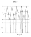
- Fig. 8 shows a PWM signal waveform in the PWM signal generating section of the first conventional technique.
- Fig. 8 shows a PWM signal waveform in the PWM signal generating section of the first conventional technique.
- symbol a denotes a signal wave; b, a carrier wave; t , time; T, a period of the carrier wave b; and PWM, a PWM signal.
- the PWM signal waveform in the first conventional technique will be described below with reference to Fig. 8 . If, for example, the PWM signal is given a value "1" when the signal wave a is larger than the carrier wave b and is otherwise given a value "0", a PWM waveform as shown in Fig. 8 is obtained. In this case, if the amplitude of the carrier wave b is assumed to be "1," average values, over one period T of the carrier wave b, of the signal wave a and the PWM signal are approximately the same.
- Fig. 9 shows the configuration of a PWM signal generating section of a PWM inverter in a second conventional technique.
- numeral 3 denotes a comparator for comparing a signal wave and a carrier wave
- numeral 4 denotes a trigonometric function calculating section.
- Symbol A denotes a desired amplitude; ⁇ , a desired phase; al, a signal wave; b, a carrier wave; and PWM, a PWM signal.
- Fig. 10 shows a PWM signal waveform in the PWM signal generating section of the second conventional technique.
- Fig. 10 shows a PWM signal waveform in the PWM signal generating section of the second conventional technique.
- symbol a and a1 denote signal waves; b, a carrier wave; t, t1, and t2, time and time points; T, a period of the carrier wave b; and PWM, a PWM signal.
- the operation of the PWM signal generating section of the PWM inverter of the second conventional technique will be described below with reference to Figs. 9 and 10 .
- a signal wave a is generated frequently (commonly) using a trigonometric function on the basis of two data, that is, an amplitude A and a phase ⁇ .
- a signal wave a1 is given by Equation (1):
- Equation (1) is executed in a certain control cycle.
- the signal wave a1 is generated by quantization whose period is equal to the carrier wave period T.
- the signal wave a1 is given a waveform as shown in Fig. 10 .
- the comparator 3 performs comparison using such a signal wave a1.
- the PWM signal that is generated and output by using the conventional technique is a signal that is delayed from the signal wave a and thus the amplitude A and the phase ⁇ are not transmitted correctly. This will be checked below in a period of time t 1 to t 2 (arrow portion in Fig. 10 ).
- the phase of the signal wave a waveform advances ⁇ (t 2 - t 1 ) in time period t 1 to t 2 .
- the phase of the generated PWM waveform remains, for the one period T, the phase ⁇ t 1 at time t 1 when the one cycle starts. This is because the signal wave a1 which is generated by quantization whose period that is equal to the carrier wave period T is sampled at time t 1 .
- the present invention has been made in view of the above problems, and an object of the present invention is to provide a PWM inverter capable of preventing a phase error from occurring in generating a PWM signal even in the case where the frequency of a carrier wave is not sufficiently higher than that of a signal wave.
- a PWM inverter includes: a DC-to-AC converting section for converting a DC voltage into an AC voltage; and a PWM signal generating section for generating a PWM signal by comparing an instructed, desired signal wave with a carrier wave, the PWM signal serving to control the AC voltage.
- the PWM signal generating section includes a phase adjusting section for advancing a phase by adding, to the signal wave, a phase delay component of the PWM signal with respect to the signal wave, the phase delay component being involved by digital control.
- the carrier wave has a periodic waveform such as a triangular wave or a sawtooth wave that is synchronized with control cycles for generating the signal wave.
- the PWM signal generating section advances the phase of the signal wave by adding, to the signal wave, a phase corresponding to a half of a control period divided by a ratio of the control frequency with respect to the carrier wave frequency.
- the PWM signal generating section further includes: a carrier wave frequency changing section for changing a carrier wave frequency; and a carrier wave generating section for generating a carrier wave according to the changed frequency.
- the phase adjusting section adds a phase component according to a ratio of a control period with respect to the carrier wave frequency, to a desired phase in synchronism with the change of the carrier wave frequency.
- the first aspect of the present invention it is possible to prevent a phase error from occurring in generating a PWM waveform, that is, it is possible to prevent phase delay of a PWM waveform from a desired signal wave.
- the second aspect of the present invention it is possible to prevent a phase error from occurring in generating a PWM waveform, that is, it is possible to prevent phase delay of a PWM waveform from a desired signal wave in the case where the carrier wave has a periodic waveform such as a triangular wave or a sawtooth wave.
- the third aspect of the present invention it is possible to prevent a phase error from occurring in generating a PWM waveform, that is, it is possible to prevent phase delay of a PWM waveform from a desired signal wave in the case where the control frequency for generating the desired signal wave is equal to the carrier wave frequency multiplied by the certain number.
- a phase error from occurring in generating a PWM waveform that is, it is possible to prevent phase delay of a PWM waveform from a desired signal wave even if the carrier wave frequency is changed.
- Fig. 1 shows the configuration of a PWM signal generating section of a PWM inverter according to a first embodiment of the present invention.
- numeral 1 denotes a DC-to-AC converting section; 2, a PWM signal generating section; 3, a comparator for comparing a signal wave and a carrier wave; 4, a trigonometric function calculating section; 5, a DC input; 6, an AC output; and 11, a phase adjusting section.
- Symbol A denotes a desired amplitude; ⁇ , a desired phase; ⁇ , a phase by which to advance a signal wave; a2, a signal wave; b, a carrier wave; and PWM, a PWM signal.
- the PWM signal generating section 2 is equipped with the phase adjusting section 11 for advancing the phase by adding, to a signal wave, a digital-control-induced phase delay component ⁇ of a PWM signal with respect to the signal wave.
- a signal a1 is generated by digital control from two data (amplitude A and phase ⁇ ) by using a trigonometric function in the trigonometric function calculating section 4 with its cycles synchronized with the frequency of a carrier wave b.
- Equation (3) is given by expressing the phase ⁇ by the angular frequency ⁇ and time t in the above-mentioned Equation (1):
- the PWM inverter is characterized in that the phase of a signal wave is advanced by a phase ⁇ to prevent a phase delay of a PWM waveform with respect to a signal wave from occurring in generating the PWM waveform.
- the phase error is given by Equation (2).
- the signal wave a1 in Equation (3) is represented as a signal wave a2 ( see the following Equation (4)).
- an appropriate procedure is such that the phase of a signal wave is advanced by adding a phase that corresponds to a half of the control period for generating the signal wave to the signal wave in the phase adjusting section 11 and a signal wave a2 is generated in the trigonometric function calculating section 4 on the basis of an amplitude A and the advanced phase.
- the amplitude A be equal to the amplitude of a carrier wave b.
- Fig. 2 illustrates a second embodiment of the present invention and shows a PWM signal waveform which is generated by using a sawtooth wave as a carrier wave in the PWM signal generating section.
- symbol a1 denotes a signal wave
- b1 a carrier wave
- t time
- PWM a PWM signal.
- the configuration of this embodiment is the same as that of the first embodiment ( Fig. 1 ) and hence its description will be omitted.
- the carrier wave b is a triangular wave
- a similar delay occurs in the PWM waveform even in the case where the carrier wave b 1 is a sawtooth wave as shown in Fig. 2 (this embodiment).
- Fig. 3 illustrates a third embodiment of the present invention and shows a PWM signal waveform which is generated in such a manner that the control frequency is set at two times the carrier wave frequency in the PWM signal generating section.
- symbols a and a1 denote signal waves; b, a carrier wave; t, time; T, the period of the carrier wave b; and PWM, a PWM signal.
- the configuration of this embodiment is the same as that of the first embodiment ( Fig. 1 ) and hence its description will not be omitted.
- Equation (4) of the first embodiment the control period for generating a signal wave a1 is equal to the carrier wave frequency
- a similar method can also prevent a phase error from occurring in generating a PWM wave even if the control frequency is set at integer (e.g., 2 or 3) times or 1/2 or 1/3 times the carrier wave frequency as shown in Fig. 3 .
- the control frequency is set at two times the carrier wave frequency
- the phase delay of the PWM waveform becomes half.
- B is set to the ratio of the control frequency with respect to the carrier wave frequency
- the signal wave a2 is given by Equation (5):
- a ⁇ 2 A sin ⁇ ⁇ t + T / 2 ⁇ B
- Parameter B is a natural number that is 1 or more or its reciprocal.
- Fig. 4 shows the configuration of a PWM signal generating section of a PWM inverter according to a fourth embodiment of the present invention.
- numeral 12 denotes a carrier wave frequency changing section
- numeral 13 denotes a carrier wave generating section.
- the same reference symbols as those in Fig. 1 denote the same components as those in Fig. 1 and hence their description will be omitted.
- This embodiment is different from the first embodiment of Fig. 1 in the following points. That is, in this embodiment, the carrier wave frequency changing section 12 for changing the frequency of a carrier wave and the carrier wave generating section 13 for generating a carrier wave according to a changed frequency are provided in addition to the components shown in Fig. 1 .
- the phase adjusting section 11 is configured to add, to a desired phase, a phase component that conforms to the ratio of the control period in synchronism with a change of the carrier wave frequency.
- Fig. 5 illustrates the fourth embodiment of the present invention and shows a waveform of a signal wave which is generated by using a carrier wave b2 in which the carrier wave frequency is switched halfway in the PWM signal generating section.
- a3 denotes a desired signal wave; a4, a phase-advanced signal wave; b2, a carrier wave; T1, a carrier wave period before frequency switching; T2, a carrier wave period after the frequency switching; t, time; and B1, B2, ratios of the control frequency with respect to the carrier wave frequency.
- a signal wave a2 is generated in such a manner that the phase ⁇ by which to advance the phase of a signal wave is changed according to the ratio of the control frequency with respect to the carrier wave frequency at time t 1 when the carrier wave frequency is switched.
- the carrier wave frequency should be switched with timing of coincidence of the control cycles and the carrier wave cycles, that is, at a peak or valley of the carrier wave having a triangular waveform.
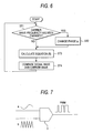
- Fig. 6 is a flowchart of a processing procedure for generating a PWM signal in the PWM inverter according to the fourth embodiment of the present invention.
- the PWM signal generating process according to the embodiment will be described in order below with reference to Fig. 6 .
- step ST1 it is checked whether the frequency of a carrier wave b has been changed by the carrier wave frequency changing section 12. If it has been changed, at step ST2 the phase updating section 13 updates the phase ⁇ by which to advance a desired signal wave according to the ratio of the control frequency with respect to the carrier wave frequency.
- the trigonometric function calculating section 4 calculates a signal wave a2 according to Equation (5).
- the amplitudes of the signal wave a2 and the carrier wave b are compared with each other by the comparator 3 and thus a PWM signal is generated.
- the PWM inverter can cope with a change of the carrier wave frequency and prevent a phase delay from occurring in generating a PWM wave because the phase of a desired signal wave is advanced from the carrier wave frequency.
- the present invention is applicable to various power converters using PWM.
Landscapes
- Engineering & Computer Science (AREA)
- Power Engineering (AREA)
- Inverter Devices (AREA)
Abstract
Description
- The present invention relates to a PWM inverter which controls the AC output voltage in DC-to-AC conversion.
-
Fig. 7 shows the configuration of a PWM signal generating section of a PWM inverter in a first conventional technique.
InFig. 7 ,numeral 3 denotes a comparator. Symbol a denotes a signal wave, b denotes a carrier wave, and PWM denotes a PWM signal.
As shown inFig. 7 , the PWM signal generating section of the conventional PWM inverter compares a signal wave a and a carrier wave b to determines an output state according to their amplitude magnitude relationship (see e.g., Patent document 1).
Fig. 8 shows a PWM signal waveform in the PWM signal generating section of the first conventional technique. InFig. 8 , symbol a denotes a signal wave; b, a carrier wave; t, time; T, a period of the carrier wave b; and PWM, a PWM signal.
The PWM signal waveform in the first conventional technique will be described below with reference toFig. 8 .
If, for example, the PWM signal is given a value "1" when the signal wave a is larger than the carrier wave b and is otherwise given a value "0", a PWM waveform as shown inFig. 8 is obtained. In this case, if the amplitude of the carrier wave b is assumed to be "1," average values, over one period T of the carrier wave b, of the signal wave a and the PWM signal are approximately the same. -
Fig. 9 shows the configuration of a PWM signal generating section of a PWM inverter in a second conventional technique. InFig. 9 ,numeral 3 denotes a comparator for comparing a signal wave and a carrier wave andnumeral 4 denotes a trigonometric function calculating section. Symbol A denotes a desired amplitude; θ, a desired phase; al, a signal wave; b, a carrier wave; and PWM, a PWM signal.
Fig. 10 shows a PWM signal waveform in the PWM signal generating section of the second conventional technique. InFig. 10 , symbol a and a1 denote signal waves; b, a carrier wave; t, t1, and t2, time and time points; T, a period of the carrier wave b; and PWM, a PWM signal.
The operation of the PWM signal generating section of the PWM inverter of the second conventional technique will be described below with reference toFigs. 9 and10 .
With the progress of the digital control in PWM inverter, in the case where vector control or the like is used, a signal wave a is generated frequently (commonly) using a trigonometric function on the basis of two data, that is, an amplitude A and a phase θ. In this case, a signal wave a1 is given by Equation (1): -

- Because of the digital control, Equation (1) is executed in a certain control cycle. For example, in the case where it is executed in synchronism with a carrier wave frequency, the signal wave a1 is generated by quantization whose period is equal to the carrier wave period T. As a result, the signal wave a1 is given a waveform as shown in
Fig. 10 . Thecomparator 3 performs comparison using such a signal wave a1. - As described above, in the PWM signal generating section of the conventional PWM inverter, digital control is used in generating a signal wave a1 from two data (amplitude A and phase θ) using a trigonometric function. The signal wave a1 and a carrier wave b are compared by the
comparator 3 to determine an output state according to their amplitude magnitude relationship.
Patent document 1:JP-A-2000-102257 Fig. 3 ) - However, there is a problem in that the PWM signal that is generated and output by using the conventional technique is a signal that is delayed from the signal wave a and thus the amplitude A and the phase θ are not transmitted correctly. This will be checked below in a period of time t1 to t2 (arrow portion in
Fig. 10 ). The phase of the signal wave a waveform advances ω(t2 - t1) in time period t1 to t2. On the other hand, the phase of the generated PWM waveform remains, for the one period T, the phase ωt1 at time t1 when the one cycle starts. This is because the signal wave a1 which is generated by quantization whose period that is equal to the carrier wave period T is sampled at time t1. In this case, ω is the angular frequency of the signal wave a (ω = θ/t). Therefore, in the period T, the phase of the signal wave a is equal to ω(t2 + t1)/2 and hence has an error Δθ (see the following Equation (2)) from the phase of the PWM waveform: -

- As seen from Equation (2), there is a problem in that this phase error is large when the frequency of the carrier wave b is not sufficiently higher than that of the signal wave a.
- The present invention has been made in view of the above problems, and an object of the present invention is to provide a PWM inverter capable of preventing a phase error from occurring in generating a PWM signal even in the case where the frequency of a carrier wave is not sufficiently higher than that of a signal wave.
- To solve the above problem, according to a first aspect of the present invention, there is provided a PWM inverter includes: a DC-to-AC converting section for converting a DC voltage into an AC voltage; and a PWM signal generating section for generating a PWM signal by comparing an instructed, desired signal wave with a carrier wave, the PWM signal serving to control the AC voltage. The PWM signal generating section includes a phase adjusting section for advancing a phase by adding, to the signal wave, a phase delay component of the PWM signal with respect to the signal wave, the phase delay component being involved by digital control.
- According to a second aspect of the present invention, in the PWM inverter according to the first aspect, the carrier wave has a periodic waveform such as a triangular wave or a sawtooth wave that is synchronized with control cycles for generating the signal wave.
- According to a third aspect of the present invention, in the PWM inverter according to the first aspect, in a case where a control frequency for generating the signal wave is equal to a carrier wave frequency multiplied by a certain number, the PWM signal generating section advances the phase of the signal wave by adding, to the signal wave, a phase corresponding to a half of a control period divided by a ratio of the control frequency with respect to the carrier wave frequency.
- According to a fourth aspect of the present invention, in the PWM inverter according to the first aspect, the PWM signal generating section further includes: a carrier wave frequency changing section for changing a carrier wave frequency; and a carrier wave generating section for generating a carrier wave according to the changed frequency. The phase adjusting section adds a phase component according to a ratio of a control period with respect to the carrier wave frequency, to a desired phase in synchronism with the change of the carrier wave frequency.
- According to the first aspect of the present invention, it is possible to prevent a phase error from occurring in generating a PWM waveform, that is, it is possible to prevent phase delay of a PWM waveform from a desired signal wave.
- According to the second aspect of the present invention, it is possible to prevent a phase error from occurring in generating a PWM waveform, that is, it is possible to prevent phase delay of a PWM waveform from a desired signal wave in the case where the carrier wave has a periodic waveform such as a triangular wave or a sawtooth wave.
- According to the third aspect of the present invention, it is possible to prevent a phase error from occurring in generating a PWM waveform, that is, it is possible to prevent phase delay of a PWM waveform from a desired signal wave in the case where the control frequency for generating the desired signal wave is equal to the carrier wave frequency multiplied by the certain number.
- According to a fourth aspect of the present invention, it is possible to prevent a phase error from occurring in generating a PWM waveform, that is, it is possible to prevent phase delay of a PWM waveform from a desired signal wave even if the carrier wave frequency is changed.
-
-
Fig. 1 shows the configuration of a PWM signal generating section of a PWM inverter according to a first embodiment of the present invention; -
Fig. 2 illustrates a second embodiment of the present invention and shows a PWM signal waveform which is generated by using a sawtooth wave as a carrier wave in the PWM signal generating section; -
Fig. 3 illustrates a third embodiment of the present invention and shows a PWM signal waveform which is generated in such a manner that the control frequency is set at two times the carrier wave frequency in the PWM signal generating section; -
Fig. 4 shows the configuration of a PWM signal generating section of a PWM inverter according to a fourth embodiment of the present invention; -
Fig. 5 illustrates a fourth embodiment of the present invention and shows a waveform of a signal wave which is generated by using a carrier wave b2 in which the carrier wave frequency is switched halfway in the PWM signal generating section of the present invention; -
Fig. 6 is a flowchart of a processing procedure for generating a PWM signal in the PWM inverter according to the fourth embodiment of the present invention; -
Fig. 7 shows the configuration of a PWM signal generating section of a PWM inverter in a first conventional technique; -
Fig. 8 shows a PWM signal waveform in the PWM signal generating section of the first conventional technique; -
Fig. 9 shows the configuration of a PWM signal generating section of a PWM inverter in a second conventional technique; and -
Fig. 10 shows a PWM signal waveform in the PWM signal generating section of the second conventional technique. -
- 1: DC-to-AC converting section
- 2: PWM signal generating section
- 3: Comparator
- 4: Trigonometric function calculating section
- 5: DC input
- 6: AC output
- 11: Phase adjusting section
- 12: Carrier wave frequency changing section
- 13: Carrier wave generating section
- a, a1, a2: Signal wave
- a3: Desired signal wave
- a4: Phase-advanced signal wave
- b, b1, b2: Carrier wave
- A: Amplitude
- θ, φ: Phase
- T, T1, T2: Period
- B1, B2: Ratio of control frequency to carrier wave frequency
- t: time
- PWM: PWM signal
- Specific embodiments of a method of the present invention will be hereinafter described with reference to the drawings.
-
Fig. 1 shows the configuration of a PWM signal generating section of a PWM inverter according to a first embodiment of the present invention.
InFig. 1 ,numeral 1 denotes a DC-to-AC converting section; 2, a PWM signal generating section; 3, a comparator for comparing a signal wave and a carrier wave; 4, a trigonometric function calculating section; 5, a DC input; 6, an AC output; and 11, a phase adjusting section. Symbol A denotes a desired amplitude; θ, a desired phase; φ, a phase by which to advance a signal wave; a2, a signal wave; b, a carrier wave; and PWM, a PWM signal.
This embodiment is different from the second conventional technique ofFig. 9 in the following point.
That is, in the PWM inverter according to the present embodiment, the PWMsignal generating section 2 is equipped with thephase adjusting section 11 for advancing the phase by adding, to a signal wave, a digital-control-induced phase delay component φ of a PWM signal with respect to the signal wave. - The operation of the PWM
signal generating section 2 of the PWM inverter according to the embodiment will be described below with reference toFig. 1 .
A signal a1 is generated by digital control from two data (amplitude A and phase θ) by using a trigonometric function in the trigonometricfunction calculating section 4 with its cycles synchronized with the frequency of a carrier wave b.
Equation (3) is given by expressing the phase θ by the angular frequency ω and time t in the above-mentioned Equation (1): -

- The PWM inverter according to the present embodiment is characterized in that the phase of a signal wave is advanced by a phase φ to prevent a phase delay of a PWM waveform with respect to a signal wave from occurring in generating the PWM waveform. In the case where the period of the digital control is equal to the carrier wave period as in the case of
Fig. 10 , as described above the phase error is given by Equation (2). The signal wave a1 in Equation (3) is represented as a signal wave a2 (see the following Equation (4)). That is, an appropriate procedure is such that the phase of a signal wave is advanced by adding a phase that corresponds to a half of the control period for generating the signal wave to the signal wave in thephase adjusting section 11 and a signal wave a2 is generated in the trigonometricfunction calculating section 4 on the basis of an amplitude A and the advanced phase. -

- In this case, it is necessary that the amplitude A be equal to the amplitude of a carrier wave b.
-
Fig. 2 illustrates a second embodiment of the present invention and shows a PWM signal waveform which is generated by using a sawtooth wave as a carrier wave in the PWM signal generating section. InFig. 2 , symbol a1 denotes a signal wave; b1, a carrier wave; t, time; and PWM, a PWM signal. The configuration of this embodiment is the same as that of the first embodiment (Fig. 1 ) and hence its description will be omitted.
Whereas inFig. 1 (first embodiment) the carrier wave b is a triangular wave, a similar delay occurs in the PWM waveform even in the case where thecarrier wave b 1 is a sawtooth wave as shown inFig. 2 (this embodiment). Therefore, in the case where the waveform update cycles are synchronized with the carrier wave frequency as in the signal wave a1, it is possible to prevent a phase error from occurring in generating a PWM waveform by advancing the phase of the signal wave as indicated by the above-mentioned Equation (4). -
Fig. 3 illustrates a third embodiment of the present invention and shows a PWM signal waveform which is generated in such a manner that the control frequency is set at two times the carrier wave frequency in the PWM signal generating section. InFig. 3 , symbols a and a1 denote signal waves; b, a carrier wave; t, time; T, the period of the carrier wave b; and PWM, a PWM signal. The configuration of this embodiment is the same as that of the first embodiment (Fig. 1 ) and hence its description will not be omitted.
Whereas in Equation (4) of the first embodiment the control period for generating a signal wave a1 is equal to the carrier wave frequency, a similar method can also prevent a phase error from occurring in generating a PWM wave even if the control frequency is set at integer (e.g., 2 or 3) times or 1/2 or 1/3 times the carrier wave frequency as shown inFig. 3 . In the case where the control frequency is set at two times the carrier wave frequency, the phase delay of the PWM waveform becomes half. When B is set to the ratio of the control frequency with respect to the carrier wave frequency, the signal wave a2 is given by Equation (5): -

- Parameter B is a natural number that is 1 or more or its reciprocal.
-
Fig. 4 shows the configuration of a PWM signal generating section of a PWM inverter according to a fourth embodiment of the present invention. InFig. 4 , numeral 12 denotes a carrier wave frequency changing section and numeral 13 denotes a carrier wave generating section. InFig. 4 , the same reference symbols as those inFig. 1 denote the same components as those inFig. 1 and hence their description will be omitted.
This embodiment is different from the first embodiment ofFig. 1 in the following points.
That is, in this embodiment, the carrier wavefrequency changing section 12 for changing the frequency of a carrier wave and the carrierwave generating section 13 for generating a carrier wave according to a changed frequency are provided in addition to the components shown inFig. 1 . Also, thephase adjusting section 11 is configured to add, to a desired phase, a phase component that conforms to the ratio of the control period in synchronism with a change of the carrier wave frequency. -
Fig. 5 illustrates the fourth embodiment of the present invention and shows a waveform of a signal wave which is generated by using a carrier wave b2 in which the carrier wave frequency is switched halfway in the PWM signal generating section. InFig. 5 , a3 denotes a desired signal wave; a4, a phase-advanced signal wave; b2, a carrier wave; T1, a carrier wave period before frequency switching; T2, a carrier wave period after the frequency switching; t, time; and B1, B2, ratios of the control frequency with respect to the carrier wave frequency.
As shown inFig. 5 , a signal wave a2 is generated in such a manner that the phase φ by which to advance the phase of a signal wave is changed according to the ratio of the control frequency with respect to the carrier wave frequency at time t1 when the carrier wave frequency is switched. However, the carrier wave frequency should be switched with timing of coincidence of the control cycles and the carrier wave cycles, that is, at a peak or valley of the carrier wave having a triangular waveform. -
Fig. 6 is a flowchart of a processing procedure for generating a PWM signal in the PWM inverter according to the fourth embodiment of the present invention.
The PWM signal generating process according to the embodiment will be described in order below with reference toFig. 6 .
First, at step ST1, it is checked whether the frequency of a carrier wave b has been changed by the carrier wavefrequency changing section 12. If it has been changed, at step ST2 thephase updating section 13 updates the phase φ by which to advance a desired signal wave according to the ratio of the control frequency with respect to the carrier wave frequency. At step ST3, the trigonometricfunction calculating section 4 calculates a signal wave a2 according to Equation (5). At step ST4, the amplitudes of the signal wave a2 and the carrier wave b are compared with each other by thecomparator 3 and thus a PWM signal is generated. - As described above, in the PWM inverter according to this embodiment can cope with a change of the carrier wave frequency and prevent a phase delay from occurring in generating a PWM wave because the phase of a desired signal wave is advanced from the carrier wave frequency.
- The present invention is applicable to various power converters using PWM.
-
-
FIG. 6 - START
- ST1: CARRIER WAVE FREQUENCY HAS BEEN CHANGED?
- ST2: CHANGE PHASE φ.
- ST3: CALCULATE EQUATION (5).
- ST4: COMPARE SIGNAL WAVE AND CARRIER WAVE.
Claims (4)
- A PWM inverter, comprising:a DC-to-AC converting section for converting a DC voltage into an AC voltage; anda PWM signal generating section for generating a PWM signal by comparing an instructed, desired signal wave with a carrier wave, the PWM signal serving to control the AC voltage,wherein the PWM signal generating section comprises a phase adjusting section for advancing a phase by adding, to the signal wave, a phase delay component of the PWM signal with respect to the signal wave, the phase delay component being involved by digital control.
- The PWM inverter according to claim 1, wherein the carrier wave has a periodic waveform such as a triangular wave or a sawtooth wave that is synchronized with control cycles for generating the signal wave.
- The PWM inverter according to claim 1, wherein in a case where a control frequency for generating the signal wave is equal to a carrier wave frequency multiplied by a certain number, the PWM signal generating section advances the phase of the signal wave by adding, to the signal wave, a phase corresponding to a half of a control period divided by a ratio of the control frequency with respect to the carrier wave frequency-.
- The PWM inverter according to claim 1, wherein the PWM signal generating section further comprises:a carrier wave frequency changing section for changing a carrier wave frequency; anda carrier wave generating section for generating a carrier wave according to the changed frequency,wherein the phase adjusting section adds a phase component according to a ratio of a control period with respect to the carrier wave frequency, to a desired phase in synchronism with the change of the carrier wave frequency.
Applications Claiming Priority (2)
| Application Number | Priority Date | Filing Date | Title |
|---|---|---|---|
| JP2006105628 | 2006-04-06 | ||
| PCT/JP2007/054323 WO2007113972A1 (en) | 2006-04-06 | 2007-03-06 | Pwm inverter device |
Publications (2)
| Publication Number | Publication Date |
|---|---|
| EP2006990A1 true EP2006990A1 (en) | 2008-12-24 |
| EP2006990A4 EP2006990A4 (en) | 2017-04-26 |
Family
ID=38563244
Family Applications (1)
| Application Number | Title | Priority Date | Filing Date |
|---|---|---|---|
| EP07737870.1A Withdrawn EP2006990A4 (en) | 2006-04-06 | 2007-03-06 | Pwm inverter device |
Country Status (7)
| Country | Link |
|---|---|
| US (1) | US8189356B2 (en) |
| EP (1) | EP2006990A4 (en) |
| JP (1) | JP4730435B2 (en) |
| KR (1) | KR20080109826A (en) |
| CN (1) | CN101416374B (en) |
| TW (1) | TW200740098A (en) |
| WO (1) | WO2007113972A1 (en) |
Families Citing this family (4)
| Publication number | Priority date | Publication date | Assignee | Title |
|---|---|---|---|---|
| JP5320721B2 (en) * | 2007-11-05 | 2013-10-23 | 株式会社安川電機 | PWM inverter device |
| JP4911241B1 (en) | 2010-11-16 | 2012-04-04 | ダイキン工業株式会社 | Power converter |
| CN103401447B (en) * | 2013-07-19 | 2015-09-16 | 东南大学 | A kind of modulator approach of cascade connection type PWM rectifier |
| JP6247761B2 (en) | 2013-08-06 | 2017-12-13 | ベドロック・オートメーション・プラットフォームズ・インコーポレーテッド | Method for strengthening module types in industrial control systems |
Family Cites Families (11)
| Publication number | Priority date | Publication date | Assignee | Title |
|---|---|---|---|---|
| JP3245523B2 (en) * | 1995-10-16 | 2002-01-15 | シャープ株式会社 | Inverter control method and inverter control device |
| JP3994243B2 (en) | 1998-09-21 | 2007-10-17 | 株式会社安川電機 | Power converter and its PWM pulse generation method |
| JP3634222B2 (en) | 2000-01-07 | 2005-03-30 | 富士電機機器制御株式会社 | PWM pulse generation method |
| JP3812299B2 (en) * | 2000-06-28 | 2006-08-23 | 日産自動車株式会社 | Electric vehicle motor controller |
| DE60227672D1 (en) * | 2001-08-14 | 2008-08-28 | Univ Illinois | SYSTEMS AND METHOD FOR PULSE WIDTH MODULATION |
| JP3841282B2 (en) * | 2002-03-20 | 2006-11-01 | 株式会社安川電機 | PWM inverter device |
| JP2004289985A (en) * | 2003-03-25 | 2004-10-14 | Matsushita Electric Ind Co Ltd | Inverter control device for motor drive and air conditioner |
| GB2423198B (en) * | 2003-09-30 | 2006-12-13 | Misubishi Denki Kabushiki Kais | Inverter Device |
| JP4681830B2 (en) * | 2004-06-24 | 2011-05-11 | パナソニック株式会社 | PWM circuit and PWM circuit control method |
| US7157952B2 (en) * | 2004-08-20 | 2007-01-02 | L-3 Integrated Systems Company | Systems and methods for implementing delay line circuitry |
| CN100413200C (en) * | 2005-03-10 | 2008-08-20 | 上海交通大学 | Inverse Control Current Tracking Control Method Based on Average Current Compensation |
-
2007
- 2007-03-06 US US12/295,926 patent/US8189356B2/en active Active
- 2007-03-06 EP EP07737870.1A patent/EP2006990A4/en not_active Withdrawn
- 2007-03-06 KR KR1020087024386A patent/KR20080109826A/en not_active Ceased
- 2007-03-06 JP JP2008508468A patent/JP4730435B2/en active Active
- 2007-03-06 WO PCT/JP2007/054323 patent/WO2007113972A1/en not_active Ceased
- 2007-03-06 CN CN2007800120783A patent/CN101416374B/en active Active
- 2007-03-14 TW TW096108799A patent/TW200740098A/en unknown
Non-Patent Citations (1)
| Title |
|---|
| See references of WO2007113972A1 * |
Also Published As
| Publication number | Publication date |
|---|---|
| KR20080109826A (en) | 2008-12-17 |
| WO2007113972A1 (en) | 2007-10-11 |
| US20090161393A1 (en) | 2009-06-25 |
| US8189356B2 (en) | 2012-05-29 |
| CN101416374A (en) | 2009-04-22 |
| JP4730435B2 (en) | 2011-07-20 |
| TW200740098A (en) | 2007-10-16 |
| JPWO2007113972A1 (en) | 2009-08-13 |
| CN101416374B (en) | 2011-12-07 |
| EP2006990A4 (en) | 2017-04-26 |
Similar Documents
| Publication | Publication Date | Title |
|---|---|---|
| EP2017947B1 (en) | Matrix converter, and control method for the matrix converter | |
| EP2378655A1 (en) | Method for detecting output current from serial multiplex inverter | |
| US8189356B2 (en) | PWM inverter | |
| EP1528685B1 (en) | Method and apparatus for converting a PWM signal to an analog output voltage | |
| EP2642655B1 (en) | Power conversion apparatus | |
| EP2077621B1 (en) | Reference signal generation circuit, angle converter, and angle detection apparatus | |
| JPWO2010004754A1 (en) | Test apparatus, test method, and phase shifter | |
| US8472559B2 (en) | Polar transmitter and related signal transmitting method | |
| JP4557947B2 (en) | Clock data recovery device | |
| KR100386228B1 (en) | Radio communication apparatus and radio frequency correcting method | |
| EP2324612B1 (en) | Digital polar transmitter with reduced phase error for wireless communication systems | |
| WO2006135058A1 (en) | Time interval measuring apparatus and jitter measuring apparatus using the same | |
| CN112994507B (en) | PWM pulse generation method and PWM pulse generation device | |
| JP5131167B2 (en) | Clock generating apparatus and clock generating method | |
| JP4757663B2 (en) | Voltage source current control inverter | |
| EP2003779A9 (en) | Pll device | |
| EP3748859A1 (en) | Dac device having positive dac and negative dac and associated digital-to-analog converting method | |
| CN120814163B (en) | Phase correction device and phase correction method for synchronous PWM control | |
| JP4176709B2 (en) | AC / DC bidirectional converter | |
| CN106982058A (en) | Frequency eliminator and control method thereof | |
| JP4593261B2 (en) | Frequency synthesizer and reference signal phase setting method thereof | |
| JP5849672B2 (en) | Synchronous detection device | |
| JPH10126162A (en) | Phase detector | |
| JP2017220721A (en) | Phase error correction device and wireless transmitter |
Legal Events
| Date | Code | Title | Description |
|---|---|---|---|
| PUAI | Public reference made under article 153(3) epc to a published international application that has entered the european phase |
Free format text: ORIGINAL CODE: 0009012 |
|
| 17P | Request for examination filed |
Effective date: 20081006 |
|
| AK | Designated contracting states |
Kind code of ref document: A1 Designated state(s): DE |
|
| DAX | Request for extension of the european patent (deleted) | ||
| RBV | Designated contracting states (corrected) |
Designated state(s): DE |
|
| RA4 | Supplementary search report drawn up and despatched (corrected) |
Effective date: 20170327 |
|
| RIC1 | Information provided on ipc code assigned before grant |
Ipc: H02M 7/48 20070101AFI20170321BHEP Ipc: H03K 7/08 20060101ALI20170321BHEP Ipc: H02M 7/5395 20060101ALI20170321BHEP |
|
| STAA | Information on the status of an ep patent application or granted ep patent |
Free format text: STATUS: THE APPLICATION IS DEEMED TO BE WITHDRAWN |
|
| 18D | Application deemed to be withdrawn |
Effective date: 20171003 |